

UM2742
User manual
High-power RFID reader system based on ST25RU3993
Introduction
The ST25RU3993-HPEV is a high-power RAIN® (UHF) RFID reader system based on the
integrated reader IC ST25RU3993.
The purpose of ST25RU3993-HPEV is to provide a comprehensive RAIN RFID reader
system that allows the user to evaluate the properties and the features of ST25RU3993. To
achieve this goal the ST25RU3993-HPEV board, differently from a typical reference design
approach, combines a high RF power and a low RF power RFID reader on a single PCB.
Additionally, the ST25RU3993-HPEV board has been outfitted with numerous easy to
access test points and measurement possibilities. With minor modification effort it is
possible to change the architecture of the reader. For example, it is possible to control the
RF circuitry with external MCU or vice versa. Bypassing the external on-board power
amplifier or alternate antenna configurations are additional possibilities.
The ST25RU3993-HPEV is controlled by a graphical user interface (GUI) running on a host
PC. The corresponding interface is a USB/UART bridge (requires driver installation). The
GUI can be found on dedicated pages on www.st.com.
The board supports tuning the radio frequency from 840 to 960 MHz. and provides two SMB
(male) antenna connectors that can be controlled via the GUI. To enable scanning for RAIN
RFID transponders connect a suitable 50
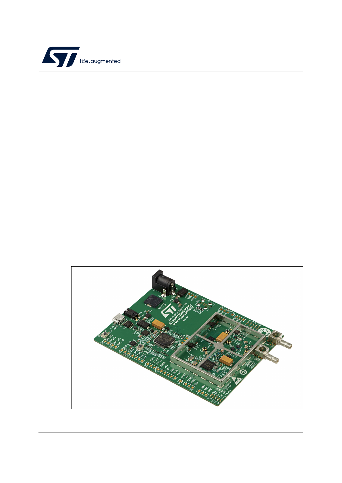
Figure 1. ST25RU3993-HPEV board
Ω UHF antenna for the targeted frequency range.
November 2020 UM2742 Rev 2 1/44
www.st.com
1

Contents UM2742
Contents
1 Standard connection setup . . . . . . . . . . . . . . . . . . . . . . . . . . . . . . . . . . . 5
1.1 Board features . . . . . . . . . . . . . . . . . . . . . . . . . . . . . . . . . . . . . . . . . . . . . . 5
2 Hardware description . . . . . . . . . . . . . . . . . . . . . . . . . . . . . . . . . . . . . . . . 9
2.1 RF circuit . . . . . . . . . . . . . . . . . . . . . . . . . . . . . . . . . . . . . . . . . . . . . . . . . . 9
2.2 Microcontroller and connections . . . . . . . . . . . . . . . . . . . . . . . . . . . . . . . . 12
2.3 Firmware programming . . . . . . . . . . . . . . . . . . . . . . . . . . . . . . . . . . . . . . 17
2.4 Boot mode . . . . . . . . . . . . . . . . . . . . . . . . . . . . . . . . . . . . . . . . . . . . . . . . 19
2.5 Power supply . . . . . . . . . . . . . . . . . . . . . . . . . . . . . . . . . . . . . . . . . . . . . . 19
2.6 Test points . . . . . . . . . . . . . . . . . . . . . . . . . . . . . . . . . . . . . . . . . . . . . . . . 22
2.6.1 Analog test points . . . . . . . . . . . . . . . . . . . . . . . . . . . . . . . . . . . . . . . . . 23
2.6.2 Digital test points . . . . . . . . . . . . . . . . . . . . . . . . . . . . . . . . . . . . . . . . . . 24
2.6.3 Probing RF signals . . . . . . . . . . . . . . . . . . . . . . . . . . . . . . . . . . . . . . . . 24
3 Schematics . . . . . . . . . . . . . . . . . . . . . . . . . . . . . . . . . . . . . . . . . . . . . . . 27
4 PCB . . . . . . . . . . . . . . . . . . . . . . . . . . . . . . . . . . . . . . . . . . . . . . . . . . . . . . 37
5 Electrical characteristics . . . . . . . . . . . . . . . . . . . . . . . . . . . . . . . . . . . . 42
6 Revision history . . . . . . . . . . . . . . . . . . . . . . . . . . . . . . . . . . . . . . . . . . . 43
2/44 UM2742 Rev 2

UM2742 List of tables
List of tables
Table 1. TXCO / Crystal configuration . . . . . . . . . . . . . . . . . . . . . . . . . . . . . . . . . . . . . . . . . . . . . . . . 9
Table 2. MCU interfaces and buttons (see Figure 5) . . . . . . . . . . . . . . . . . . . . . . . . . . . . . . . . . . . . 12
Table 3. MCU - SPI interface and ST25RU3993 connections . . . . . . . . . . . . . . . . . . . . . . . . . . . . . 14
Table 4. SPI interface pinout at J10, J12 and J13 . . . . . . . . . . . . . . . . . . . . . . . . . . . . . . . . . . . . . . 14
Table 5. UART connections and pinout . . . . . . . . . . . . . . . . . . . . . . . . . . . . . . . . . . . . . . . . . . . . . . 15
Table 6. MCU connections to buttons. . . . . . . . . . . . . . . . . . . . . . . . . . . . . . . . . . . . . . . . . . . . . . . . 15
Table 7. MCU connections to LEDs . . . . . . . . . . . . . . . . . . . . . . . . . . . . . . . . . . . . . . . . . . . . . . . . . 16
Table 8. MCU connections to RF switches . . . . . . . . . . . . . . . . . . . . . . . . . . . . . . . . . . . . . . . . . . . . 16
Table 9. Connections to JLINK (SWD) interface and pinout of connector . . . . . . . . . . . . . . . . . . . . 17
Table 10. Typical voltage levels . . . . . . . . . . . . . . . . . . . . . . . . . . . . . . . . . . . . . . . . . . . . . . . . . . . . . 20
Table 11. Connection of components . . . . . . . . . . . . . . . . . . . . . . . . . . . . . . . . . . . . . . . . . . . . . . . . . 20
Table 12. Connections of analog test points. . . . . . . . . . . . . . . . . . . . . . . . . . . . . . . . . . . . . . . . . . . . 23
Table 13. Supply voltages of analog test points . . . . . . . . . . . . . . . . . . . . . . . . . . . . . . . . . . . . . . . . . 23
Table 14. RF test points – Default power levels . . . . . . . . . . . . . . . . . . . . . . . . . . . . . . . . . . . . . . . . . 26
Table 15. List of schematics . . . . . . . . . . . . . . . . . . . . . . . . . . . . . . . . . . . . . . . . . . . . . . . . . . . . . . . . 27
Table 16. PCB stack . . . . . . . . . . . . . . . . . . . . . . . . . . . . . . . . . . . . . . . . . . . . . . . . . . . . . . . . . . . . . . 37
Table 17. Absolute maximum ratings . . . . . . . . . . . . . . . . . . . . . . . . . . . . . . . . . . . . . . . . . . . . . . . . . 42
Table 18. DC characteristics (VBUS = 5.0 V, 25 °C) . . . . . . . . . . . . . . . . . . . . . . . . . . . . . . . . . . . . . 42
Table 19. Document revision history . . . . . . . . . . . . . . . . . . . . . . . . . . . . . . . . . . . . . . . . . . . . . . . . . 43
UM2742 Rev 2 3/44
3

List of figures UM2742
List of figures
Figure 1. ST25RU3993-HPEV board. . . . . . . . . . . . . . . . . . . . . . . . . . . . . . . . . . . . . . . . . . . . . . . . . . 1
Figure 2. Standard connection setup . . . . . . . . . . . . . . . . . . . . . . . . . . . . . . . . . . . . . . . . . . . . . . . . . . 5
Figure 3. ST25RU3993-HPEV functional diagram. . . . . . . . . . . . . . . . . . . . . . . . . . . . . . . . . . . . . . . . 8
Figure 4. Power detector voltage characteristics . . . . . . . . . . . . . . . . . . . . . . . . . . . . . . . . . . . . . . . . 11
Figure 5. Main digital interfaces . . . . . . . . . . . . . . . . . . . . . . . . . . . . . . . . . . . . . . . . . . . . . . . . . . . . . 13
Figure 6. JLink connection using the needle adapter . . . . . . . . . . . . . . . . . . . . . . . . . . . . . . . . . . . . 18
Figure 7. Entering the Boot mode . . . . . . . . . . . . . . . . . . . . . . . . . . . . . . . . . . . . . . . . . . . . . . . . . . . 19
Figure 8. Test points . . . . . . . . . . . . . . . . . . . . . . . . . . . . . . . . . . . . . . . . . . . . . . . . . . . . . . . . . . . . . 22
Figure 9. Connection of a voltmeter / ammeter to the supply voltage test points . . . . . . . . . . . . . . . 23
Figure 10. RF test points . . . . . . . . . . . . . . . . . . . . . . . . . . . . . . . . . . . . . . . . . . . . . . . . . . . . . . . . . . . 25
Figure 11. Connecting to the RF test points with the SMA adapter . . . . . . . . . . . . . . . . . . . . . . . . . . . 26
Figure 12. System overview. . . . . . . . . . . . . . . . . . . . . . . . . . . . . . . . . . . . . . . . . . . . . . . . . . . . . . . . . 28
Figure 13. UHF RFID reader IC . . . . . . . . . . . . . . . . . . . . . . . . . . . . . . . . . . . . . . . . . . . . . . . . . . . . . . 29
Figure 14. External power amplifier . . . . . . . . . . . . . . . . . . . . . . . . . . . . . . . . . . . . . . . . . . . . . . . . . . . 30
Figure 15. Carrier cancellation circuit . . . . . . . . . . . . . . . . . . . . . . . . . . . . . . . . . . . . . . . . . . . . . . . . . 31
Figure 16. Antenna switch . . . . . . . . . . . . . . . . . . . . . . . . . . . . . . . . . . . . . . . . . . . . . . . . . . . . . . . . . . 32
Figure 17. RF shield. . . . . . . . . . . . . . . . . . . . . . . . . . . . . . . . . . . . . . . . . . . . . . . . . . . . . . . . . . . . . . . 32
Figure 18. USB supply / UART bridge . . . . . . . . . . . . . . . . . . . . . . . . . . . . . . . . . . . . . . . . . . . . . . . . . 33
Figure 19. Microcontroller . . . . . . . . . . . . . . . . . . . . . . . . . . . . . . . . . . . . . . . . . . . . . . . . . . . . . . . . . . 34
Figure 20. Supply LDOs. . . . . . . . . . . . . . . . . . . . . . . . . . . . . . . . . . . . . . . . . . . . . . . . . . . . . . . . . . . . 35
Figure 21. External interfaces and connections . . . . . . . . . . . . . . . . . . . . . . . . . . . . . . . . . . . . . . . . . . 36
Figure 22. Top layer layout . . . . . . . . . . . . . . . . . . . . . . . . . . . . . . . . . . . . . . . . . . . . . . . . . . . . . . . . . 38
Figure 23. RF GND layer (L2), GND layer (L4) and bottom layer (L6) layout . . . . . . . . . . . . . . . . . . . 39
Figure 24. Power layer (L3) layout . . . . . . . . . . . . . . . . . . . . . . . . . . . . . . . . . . . . . . . . . . . . . . . . . . . . 40
Figure 25. Routing layer (L5) layout. . . . . . . . . . . . . . . . . . . . . . . . . . . . . . . . . . . . . . . . . . . . . . . . . . . 41
4/44 UM2742 Rev 2
UM2742 Standard connection setup
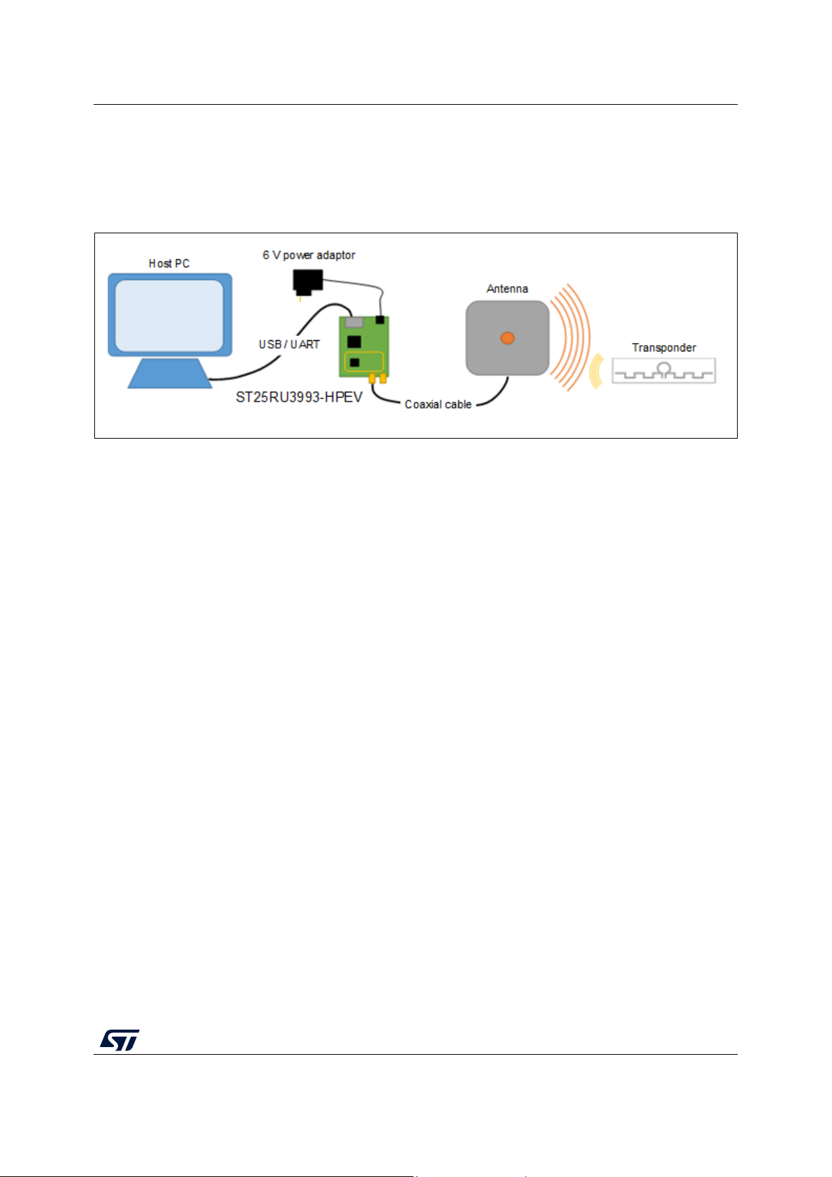
1 Standard connection setup
The typical reader setup is shown in Figure 2.
Figure 2. Standard connection setup
The host PC running the GUI is connected via a Micro-USB cable. The external power
amplifier on the ST25RU3993-HPEV board is powered through the 6 V power adapter and
must be connected when the external PA TX option is used. The antenna is connected to
the active antenna port through a coaxial cable. A transponder is within the antenna range.
1.1 Board features
ST25RU3993 RAIN (UHF) RFID reader IC
ISO/IEC 18000-63:2015 / Gen2V2
GB/T 29768-2013
Two SW-controlled power amplifier (PA) options:
– External PA: 30 dBm max. TX power
– Internal PA: 17.5 dBm max. TX power
Configurable TX power level
Power detector to monitor TX power
Automatic carrier cancellation for improved RX sensitivity
Differential RX input
RX sensitivity:
– -80 dBm at 90% read success, one sideband of tag response (ISO18046-3: 2012)
– -77 dBm at 90% read success, both sidebands of tag response
(ISO18046-3: 2020)
Adaptive / manual RX gain adjustment
Tunable radio frequency: 840 to 960 MHz
Minimum frequency step: 25 kHz
External frequency reference (20 MHz) assembly option
Adaptive / manual anti-collision slot options
Continuous wave or Modulated RF output test modes
UM2742 Rev 2 5/44
43

Standard connection setup UM2742
Two antenna ports: SMB (M)
Automatic / Manual antenna port switching
Carrier sense TX option (LBT)
UHF tag RSSI measurement
Configurable SELECT command mask
UHF transponder EPC Read / Write
Transponder read based applications trigger
Custom reader TX command editor tool
Customizable Gen2 TX commands
Direct TX modulation through MCU for proprietary protocol support
Store / Recall reader configuration
Register map
Buzzer
Host interface and supply
– USB/UART bridge
– USB receptacle: Micro, B-Type
– Main supply: 6 V DC jack
MCU:
– STM32L476RGT6 (Arm
®(a)
32-bit Cortex®-M4)
– 64 MHz
– 128-Kbyte RAM
– 1-Mbyte Flash memory
– SPI Mode 1 (5 MHz)
– Firmware programmable through USB/UART
– SWD debug interface
–LED indicators
– Power amplifier selection
– Carrier cancellation tuning activity
– Carrier cancellation tuning OK
– OSC OK (20 MHz external reference)
–PLL OK
–RF ON
– No tag response
– Tag CRC error
–Tag found
Test points:
– In-circuit RF power levels and signals
a. Arm is a registered trademark of Arm Limited (or its subsidiaries) in the US and/or elsewhere.
6/44 UM2742 Rev 2

UM2742 Standard connection setup
– RFID communication TX and RX
– UART and SPI signal lines
– UART_LOG for debugging purposes
– Control voltage of internal VCO
– RF power detector output voltage
– 20 MHz reference signal
– External PA BIAS voltage
– LDO output voltages
– LDO outputs: jumpers for current consumption measurement
– Main supply: jumper for current consumption measurement
– Antenna switch state
– Power amplifier selection switch state
Buttons:
– MCU reset
– MCU boot mode
UM2742 Rev 2 7/44
43
Standard connection setup UM2742
IRQ
EN
RF switch:
SKY13431
-
374LF
Carrier
c
ancellation
circuit
SPI (Mode 1)
5V
RX
TX
D-
D+
USB c
onnector:
MICRO-B
3.3V
3.6V
LDO:
LD39100PUR
PA_LDO_EN
PA_SW_V1
PA_SW_V2
ANT_SW_V2
ANT_SW_V1
CPL-10dB
CPL-20dB
RFOPX
RFONX
PAOUT_P
PAOUT_N
93_RF_OUT
93_intPA
PA_OUT
LP_Filter_IN
LP_Filter_OUT
TX_RX
TX
Power detector:
MAX4003EUA
ANT1
ANT2
ETC_x
MOSI
CLK
RF_Detector
SWD connector:
(
TC2050-IDC-
FP)
SWD
Buzzer:
PKMCS0909E4000
OSCO
3.3V
3.3V
3.3V
3.3V
3.3V
LDO:
LD39100PUR
LED:
MCU
LED:
RF ON
LED:
Tuning
LED:
Tuned
LED:
OSC OK
LED:
ANT1
LED:
ANT2
LED:
NO
Tag R
esp
LED:
Tag
CRC E
rr.
LED:
Tag
LED:
Int_PA
LED:
Ext_PA
LED:
PLL OK
SPI
+ IRQ + EN
Carrier
cancellation
CS
UART
UART_LOG_TX
PA_LDO_EN
OSCO
VCO
EXT_PA_BIAS
RF detector
Button:
RESET
Button:
BOOT
Legend
Component
Test point /
c
onnector
LED Button
Logic
Supply
DC power j
ack
OD: 6.4 mm
ID: 2.1 mm
6V
OSCI
Antenna selection
switch state
PA selection
switch state
LED:
BOOT (red)
VBUS 5V
VBUS 5V
USB/UART
bridge:
FT231XQ-R
Balun:
BD0810J50100AHF
20 dB coupler:
DC1722J5020A
HF
Low pass filter:
0900LP15B0063
10 dB coupler:
DC1722J5020A
HF
TCXO:
TXEAADSANF-
20
Crystal:
(optional)
NX3225SA-20
Antenna
port 2
SMB Male
Antenna
port 1
SMB Male
6V
VBUS 5V
4
3
4
RF
Analog
RF switch:
SKY13431
-
374LF
PA LDO:
LD39100PUR
RX
MIX_INP
MIX_INN
MCU:
STM32L476RG
Power
a
mplifier:
TQP9107
Balun:
BD0810J50100AHF
Balun:
0900BL15C050
UHF RFID reader IC:
ST25RU3993
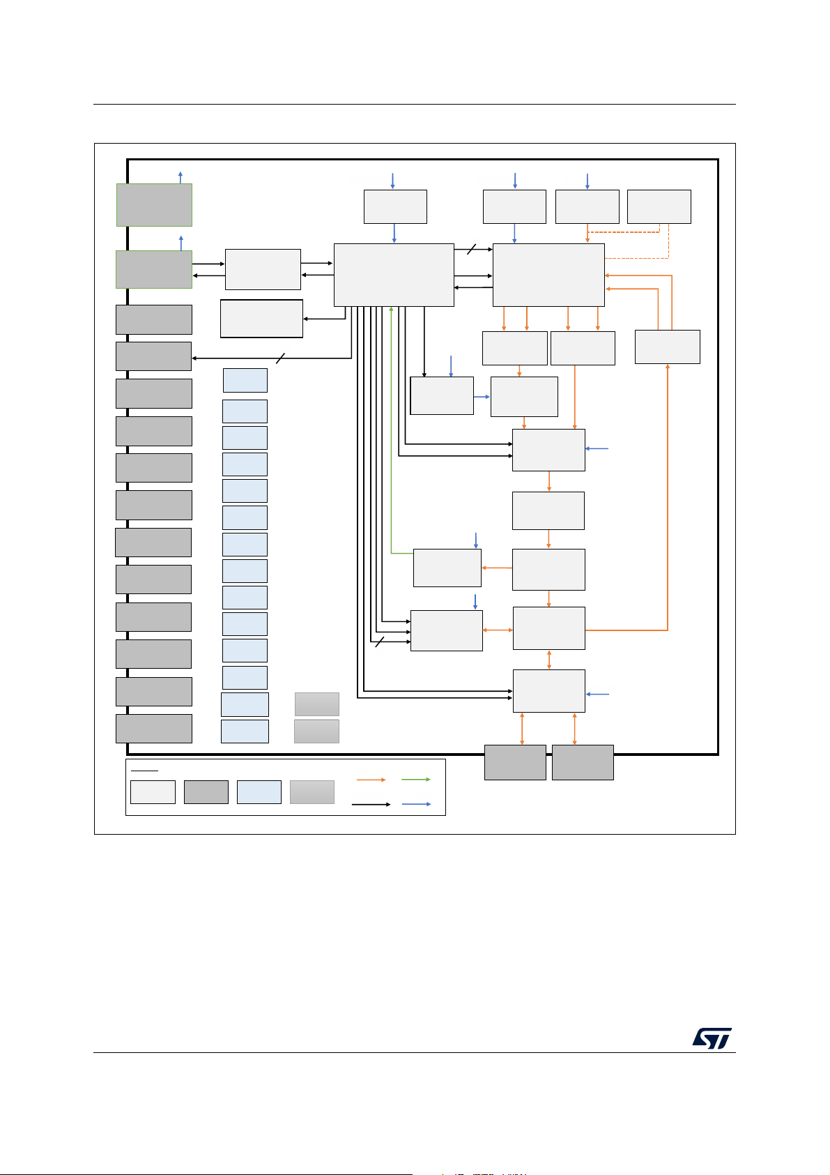
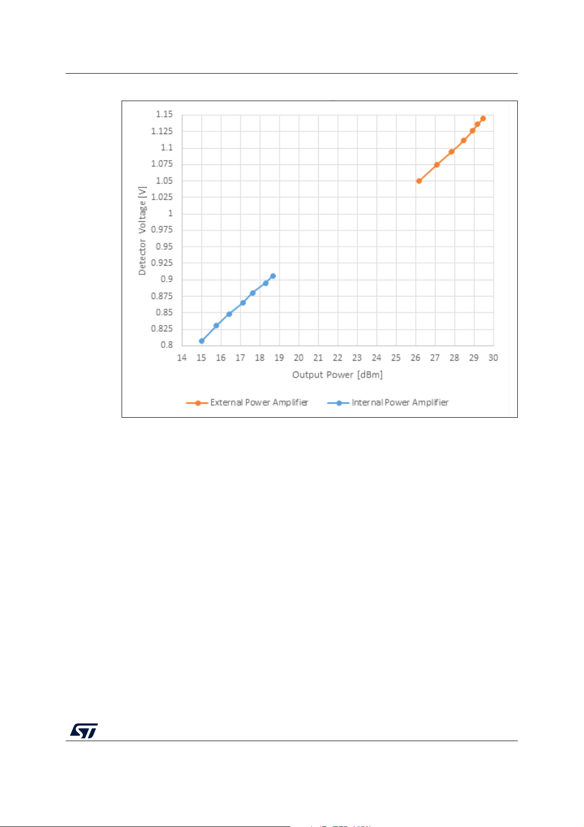
Figure 3. ST25RU3993-HPEV functional diagram
8/44 UM2742 Rev 2
UM2742 Hardware description
2 Hardware description
2.1 RF circuit
The main component of the RF circuit is the ST25RU3993 device, which receives digital
baseband transmit data and commands from the MCU via the SPI interface. It then frames
these data and automatically encodes them into PIE symbols. Based on the PIE encoded
symbols ST25RU3993 creates a sinusoidal shaped modulation signal (either ASK or
PR-ASK), which modulates the RF carrier. ST25RU3993 synthesizes its RF carrier
frequency with a VCO / integer-n phase locked loop (PLL). The frequency reference for the
PLL can be either a 20 MHz crystal oscillator or a temperature compensated crystal
oscillator (TCXO).
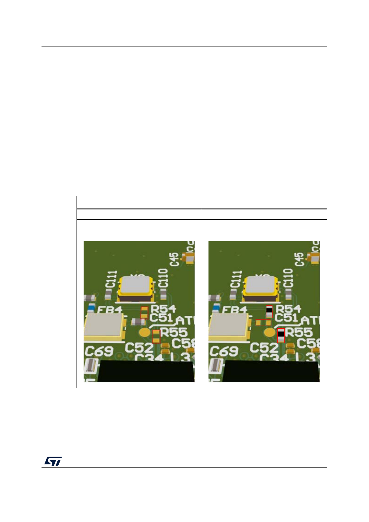
As shown in Tabl e 1 the ST25RU3993-HPEV board accommodates both options, the
default configuration is the TCXO with a clipped sine wave output wave having 0.8 Vpp
amplitude. With a small modification it is possible to connect the existing crystal.
TCXO connected to ST25RU3993 Crystal connected to ST25RU3993
R54 and R55 not populated C51 removed, R54 and R55 populated
Table 1. TXCO / Crystal configuration
Default Alternate (modified by user)
The output of the internal PLL- charge pump is connected to LF_CEXT (pin 45), and the
external part of the loop filter is placed in close proximity to it. An additional low-pass filter
stage is integrated in ST25RU3993 and is part of the loop filter circuit. The loop filter output
is the control voltage of the internal VCO.
UM2742 Rev 2 9/44
43

Hardware description UM2742
The ST25RU3993 has two differential output port pairs. The low power output and the
internal power amplifier output. Depending on which differential output port pair is activated
the modulated carrier frequency will be amplified and output accordingly.
The low power output is intended for external signal amplification for a long read range
configuration of the ST25RU3993-HPEV reader. The low power output with its differential
output pin pairs RFONX (23) and RFOPX (24) is connected to a 2:1 balun, where the
transmit signal is transformed from a 100 differential to 50
stage of the low power output is supplied by the V
DD_B
Ω single-ended signal. The output
voltage generated and regulated by
ST25RU3993 itself. L3 and L4 act as a RF choke, C57 and C58 as bypass capacitors and
C65 and C54 as DC blocking capacitors. The signal then proceeds to the external power
amplifier to generate a high-power output signal with approximately 31
dBm in
ST25RU3993-HPEV default transmit power configuration.
The internal power amplifier is used for the short read range configuration of the reader. The
output pins of the internal power amplifier are PAOUT_N (16, 17) and PAOUT_P (20, 21). A
matching network and a 1:1 balun transforms the output of the internal power amplifier to a
50
Ω single-ended signal. The internal power amplifier is supplied by the on-chip generated
and regulated voltage V
. L1, L2 are acting as RF chokes, C12 and C14 are bypass
DD_PA
capacitors. After the balun the output power of the internal power amplifier is tipically
20
dBm.
Both RF output options the external power amplifier and the output of the internal power
amplifier are connected to an RF-switch which is controlled by the PC software (GUI) of the
ST25RU3993-HPEV reader. Only one RF output option can be active at a time. Note a UHF
RFID reader reference would typically offer only one RF output and hence the PA RF-switch
would be stripped from the design avoiding it’s introduced insertion loss of ~0.5 dB. So
would be the DC blocking capacitors which this RF-switch requires on all its RF terminals.
The output of the RF-switch is connected to a low-pass filter which attenuates the second
and third harmonic of the carrier frequency. The filtered transmit signal is then connected to
a 20 dB directional coupler, which takes a negligible small portion of the transmit power,
which is further attenuated by a pi-pad attenuator. The limited TX power sample is then fed
to the input a logarithmic power detector that converts the RF power to a corresponding DC
voltage. The output DC voltage of the power detector versus the generated RF power is
shown in
Figure 4.
10/44 UM2742 Rev 2
UM2742 Hardware description
Figure 4. Power detector voltage characteristics
The DC output voltage of the power detector is connected to an ADC input pin (PA1) of the
microcontroller.
The majority of RF transmit power which passes through the 20 dB directional coupler is fed
to the main directional coupler. The main directional coupler has a coupling factor of 10 dB
and acts as the directional unit which should isolate the transmit from the receive path of
ST25RU3993. The main directional coupler plays a very important role in the RFID reader
system as its parasitics have a great influence on the sensitivity of the reader. The main
directional coupler essentially has four terminals:
1. Input
2. Direct
3. Coupled
4. Isolated
The direct terminal is connected to the second RF switch in the reader system. This switch
directs the transmit power to either antenna port 1 or antenna port 2. The antenna switch
again requires DC blocking capacitors on all its RF terminals. Both antenna ports are SMB
(male) type.
To avoid reducing the sensitivity of the reader the self-jamming signal reaching the receiving
inputs of ST25RU3993 must be minimized. The self-jamming signal comprises reflections
from the antenna (S11) and the leakage across the main directional coupler. To minimize it a
carrier cancellation circuit is connected to the coupled port of the main directional coupler.
UM2742 Rev 2 11/44
43
Hardware description UM2742
The carrier cancellation circuit is able to change its impedance and hence to reflect a certain
amount of the coupled power back into the directional coupler. This reflected signal is
combined with the self-jamming signal at the isolated port of the main directional coupler.
The isolated port of the main directional coupler is connected to the receiving pins of
ST25RU3993. If the signal reflected by the carrier cancellation circuit has the same
amplitude and opposite phase of the self-jammer the signals cancel them out and vanish.
The main components of the CCC are three digital tunable capacitors controlled by the
STM32L476RG microcontroller via SPI. The lumped components of the carrier cancellation
circuit help to define its tuning range around 50
Ω and define the impedance step created by
one LSB change of a digital tunable capacitor.
The isolated port of the main directional coupler is connected to a 2:1 balun to transform the
incoming tag response signal to a 100
Ω differential signal that is fed into ST25RU3993
receiver section at pins MIX_INP (4) and MIX_INN (6).
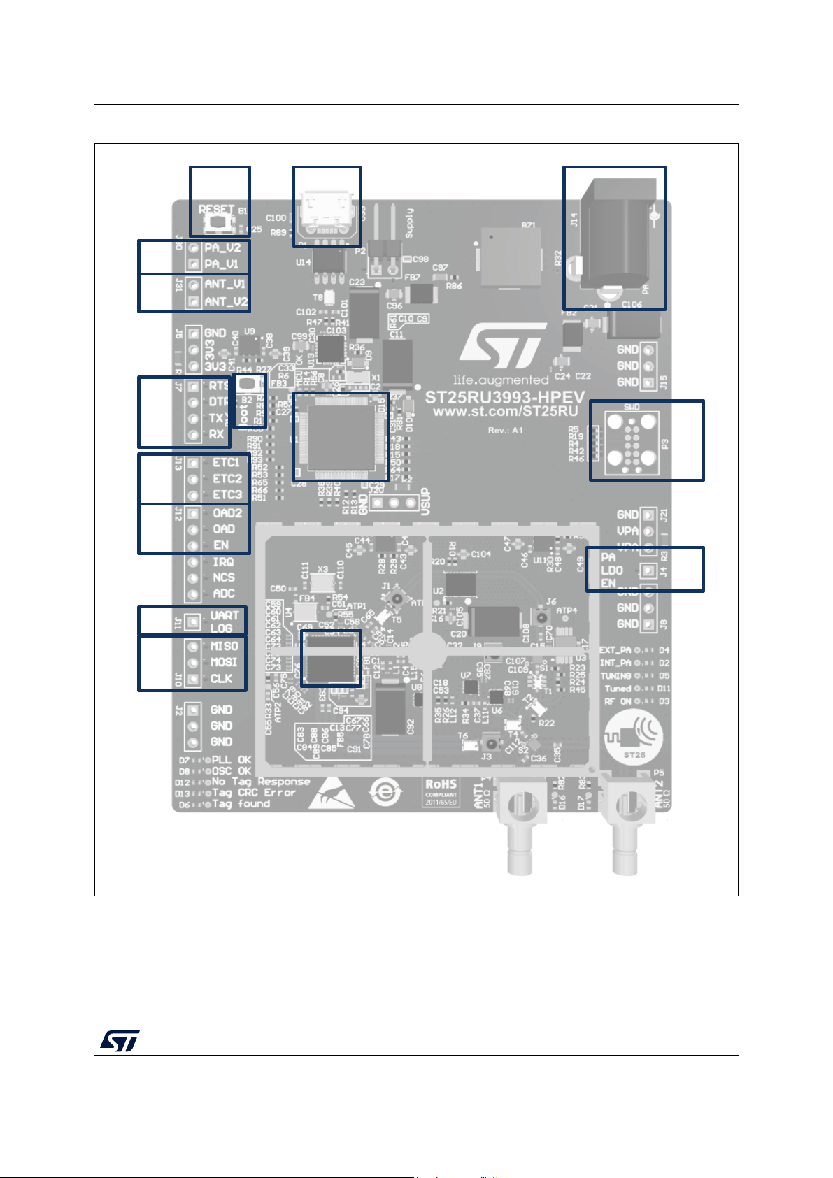
2.2 Microcontroller and connections
A MCU reset button
B USB receptacle: Micro, B-Type
C 6 V DC power connector: 5 mm barrel connector
D ST25RU3993 Rain (UHF) RFID reader IC
E Enable line connection of power amplifier LDO
F UART interface connections
G MCU boot mode button
H STM32L476RGT6 (Arm
J SWD debug interface connections
L, M SPI bus interface connections
N UART_LOG connection for debugging purposes
K Carrier cancellation circuit (CCC) SPI chip select lines
O PA output selection switch state
P Antenna port selection switch state
Table 2. MCU interfaces and buttons (see Figure 5)
®
32-bit Cortex®-M4)
12/44 UM2742 Rev 2
UM2742 Hardware description
MS53587V1
A
B
C
O
P
F
K
L
N
M
D
E
J
H
G
Figure 5. Main digital interfaces
The ST25RU3993-HPEV is controlled by STM32L476RG, a ultra-low-power MCU with FPU
Arm Cortex-M4 core, 80 MHz, 1 Mbyte Flash memory, LCD, USB OTG, DFSDM.
UM2742 Rev 2 13/44
43
Hardware description UM2742
The MCU is supplied by 3.3 Volts, regulated by an adjustable LDO. The clock source is an
external crystal generating 32.768 kHz, connected to OSC32_in (3) and OSC32_out (4). It
interfaces the host PC via UART for which a USB/UART bridge is used.
The MCU communicates with the ST25RU3993 via an SPI interface controlling the
ST25RU3993 lines ENABLE and IRQ. The SPI interface operates in mode 1 with a 6 MHz
serial clock. The SPI interface is also used to control the digital tunable capacitors for the
carrier cancellation circuit.
The MCU controls the RF switches for changing the power amplifier and the active antenna
port. The analog output of the RF power detector is connected to one of its ADC inputs
(PA1) to convert the DC voltage corresponding to the transmit RF power into a digital
representation. The LDO for the external power amplifier is enabled by the MCU, making it
possible to completely shut down the external power amplifier when RF power needs to be
OFF, e.g. as required for carrier sense (LBT). One pin (UART LOG) is reserved to act as a
generic debug pin or to be programmed as a trigger output for an external measurement
equipment.
Component U1 Component U5 Component U6 Component U7 Component U8
MCU pin ST25RU3993 pin DTC1 pin DTC2 pin DTC3 pin
Table 3. MCU - SPI interface and ST25RU3993 connections
Name Number Name Number Name Number Name Number Name Number
PA420NCS33------
PA5 21 SCLK 37 CLK 5 CLK 5 CLK 5
PA622MISO34------
PA7 23 MO SI 35 SDAT 7 SD AT 7 SDAT 7
PC738------SEN6
PC8 39 - - - - SEN 6 - -
PC9 40 - - SEN 6 - - - -
PA942IRQ32------
PA1043EN31------
Component U5 Component U6 Component U7 Component U8 J10 J12 J13
ST25RU3993 pin DTC1 pin DTC2 pin DTC3 pin
Name Number Name Number Name Number Name Number
SCLK 37 CLK 5 CLK 5 CLK 5 1 - -
MISO34------3--
MOSI 35 SDAT 7 SDAT 7 SDAT 7 2 - -
------
Table 4. SPI interface pinout at J10, J12 and J13
ETC3
SEN
6-3-
Connector
pin number
14/44 UM2742 Rev 2

UM2742 Hardware description
Table 4. SPI interface pinout at J10, J12 and J13 (continued)
Component U5 Component U6 Component U7 Component U8 J10 J12 J13
ST25RU3993 pin DTC1 pin DTC2 pin DTC3 pin
Name Number Name Number Name Number Name Number
----
--
ETC1
SEN
ETC2
SEN
6---2-
6-- - --1-
Connector
pin number
OAD2---------1
OAD---------2
EN31--------3
IRQ32--------4
NCS33--------5
ADC---------6
Table 5. UART connections and pinout
Component U1 Component U13 J7
MCU pin FTDI pin
Name Number Name Number
Connector pin
number
NRST 7 RTS 19 1
BOOT0 60 DTR 18 2
PA3 17 TXD 17 3
PA2 16 RXD 1 4
Table 6. MCU connections to buttons
Component U1 Component B1 Component B2
MCU pin Reset button Boot button
Name Number Name Number Name Number
NRST 7 1 1 2 2
BOOT0 60 - - 5 5
UM2742 Rev 2 15/44
43

Hardware description UM2742
Table 7. MCU connections to LEDs
Component U1
D1 D2 D3 D4 D5 D6 D7 D8 D11 D12 D13 D16 D17
MCU pin
Name
Number
MCU_LED
RF_LED
intPA_LED
extPA_LED
TUNING_LED
TAG _LE D
PLL_LED
OSC_LED
TUNED_LED
NO_RESP_LED
CRC_ERR_LED
ANT1_LED
ANT2_LED
PA0 141 (C)------------
PD2 54 -1 (C)-----------
PC1051 --1 (C)----------
PB4 56 ---1 (C)---------
PC1253 ----1 (C)--------
PC8 37 -----1 (C)-------
PB1233 ------1 (C)------
PB1334 -------1 (C)-----
PC1152 --------1 (C)----
PB1435 ---------1 (C)---
PB1538 ----------1 (C)--
PB2 28 -----------1 (C)-
PB1 27 ------------1 (C)
Table 8. MCU connections to RF switches
Component U1 Component S1 Component S2
MCU pin PA switch pin Antenna switch pin
Name Number Name Number Name Number
PB0 26 V1 1 - -
PC5 25 V2 3 - -
PB10 29 - - V1 1
PB11 30 - - V2 3
16/44 UM2742 Rev 2

UM2742 Hardware description
Table 9. Connections to JLINK (SWD) interface and pinout of connector
Component U1 Component P3
MCU pin JLINK pin
Name Number Name Number
--VDD1
PA1 3 46 SWDIO 2
--GND3
PA1 4 49 SWCLK 4
--GND5
PB3 55 SWO 6
--NC7
PA1 5 50 TD I 8
--NC9
NRST 7 MCU RESET N 10
2.3 Firmware programming
There are two options to program the firmware of the STM32L476RG microcontroller:
1. The simplest way to program a new firmware version to the MCU is by connecting the
ST25RU3993-HPEV board to the host PC with the micro USB cable and use the
Firmware Update function of the GUI. For more information about this option refer to
the user manual of the GUI.
2. Alternatively, the firmware can be programmed to the MCU using the ST-LINK
connected to the JLINK (SWD) interface (see
Figure 6) with a J-Link needle adapter
(e.g. 8.06.04 J-LINK 10-PIN NEEDLE ADAPTER). For more information about this
option refer to the user manual of the ST-LINK/V2.
UM2742 Rev 2 17/44
43

Hardware description UM2742
Figure 6. JLink connection using the needle adapter
18/44 UM2742 Rev 2

UM2742 Hardware description
MS53599V1
2
1
2.4 Boot mode
To enter the STM32L476RG boot mode press and hold the BOOT button (1) while the
RESET button (2) is pressed (see
buttons can be released.
Figure 7). At this point the boot mode is active and both
Figure 7. Entering the Boot mode
2.5 Power supply
The ST25RU3993-HPEV is supplied through the USB Interface (VBAT) and an external 6 V
supply connected to J14 a DC power jack. J14 has a hot inner contact with 2.1 mm diameter
suitable for a 5.5 mm barrel plug.
UM2742 Rev 2 19/44
43

Hardware description UM2742
The 5V (VBAT) supply rail is distributed to two low-dropout regulators which supply:
LDO U9 – for powering digital components (3V3),
LDO U10 - for powering RF components (VSUP)
The 6 V DC input is dedicated to supply the power amplifier supply via an LDO U11
regulating the supply rail VPA.
Voltage domain Voltage (V)
3V3 3.3
VSUP 3.6
VPA 5.0
Table 10. Typical voltage levels
Table 11. Connection of components
Voltage domain Schematic Component(s) Pin name(s) Pin number(s)
VI 6
Supply (Figure 20)U9, U10
5 V (VBUS)
USB interface
(Figure 18)
U13 VCC 12
EN 1
VI 6
6 V Supply (Figure 20)U11
EN 5
External interfaces
(Figure 21)
P3 1 1
VBAT 1
VDD 19, 32, 48, 64
3V3
Controller
(Figure 19)
Power amplifier
(Figure 14)
UHF_RFID
(Figure 13)
Carrier cancellation
(Figure 15)
U1
VDD / VREF+
NRST
BOOT0
VCC 8
U3
/SHDN 2
U4 VCC
U5 VDD_IO 38
U6, U7, U10 VDD 4
(4)
(2)
(3)
(1)
13
7
60
4
USB interface
(Figure 20)
VSUP (3.6 V)
UHF_RFID
(Figure 13)
20/44 UM2742 Rev 2
U13 VCCIO 20
U5 VEXT
(5)
U5 VEXT_PA
(6)
11
14

UM2742 Hardware description
Table 11. Connection of components (continued)
Voltage domain Schematic Component(s) Pin name(s) Pin number(s)
U2 VPD1 12
VPA (5 V)
1. Via ferrite bead FB3.
2. Via pull-up resistor R61.
3. Via push button B2.
4. Via ferrite bead FB4.
5. Via ferrite bead FB5.
6. Via ferrite bead FB1.
7. Via R21.
Power amplifier
(Figure 14)
U2 VPD2 11
U2 VCC 2
U2 VBIAS
(7)
1
UM2742 Rev 2 21/44
43

Hardware description UM2742
MS54000V1
5 V
3.3 V
VPA
VSUP
ATP3
ATP4
ATP1
Digital
ATP2
2.6 Test points
The ST25RU3993-HPEV board provides several test points (see Figure 8) that allow the
user to test and evaluate circuit nodes in the ST25RU3993 reader design.
Figure 8. Test points
22/44 UM2742 Rev 2

UM2742 Hardware description
MS54018V1
A
Remove
R3
V
2.6.1 Analog test points
Component U5 U2 U3
Pin Name Number Name Number Name Number
ATP1OSCO30----
Test
point
Pin no. Pin name Pin no. Pin name Pin no. Pin name Pin no. Pin name
ATP2 VCO (LF_CEXT) - - - -
ATP3 - - VBIAS 1 - -
ATP4 - - - - OUT 7
5 V (VBUS) 3V3 digital supply VSUP RF VPA power amplifier
P2 J5 J20 J21
1VBUS1GND1GND1GND
2 VBUS 2, 3 3V3 2, 3 VSUP 2, 3 VPA
Table 12. Connections of analog test points
Table 13. Supply voltages of analog test points
Two test points are placed at the output of the three LDOs to easily measure the regulated
voltage of each voltage domain. A GND pad is placed close to the voltage test points for
accurate voltage measurements (left side of
Figure 9).
The current consumption of the three regulated voltage domains can be measured
separately. To enable this kind of measurement a 0 Ω resistor (R3) must be removed (right
side of
Figure 9). Make sure to restore the connection once the measurement is done,
before reverting to normal operation.
Figure 9. Connection of a voltmeter / ammeter to the supply voltage test points
UM2742 Rev 2 23/44
43

Hardware description UM2742
2.6.2 Digital test points
In addition to the four test points shown above a test point for each LED connected to the
STM32L476RG controller is available.
PLL OK Indicates that the PLL of ST25RU3993 is locked and the carrier
frequency is stable.
OSC OK Active low. Indicates that the reference frequency for the PLL is stable.
No tag response :Pulled low if the sent reader command is not replied by a tag.
Tag CRC error Pulled low if a CRC error is detected within a tag response.
Tag found Pulled low every time a tag has been inventoried.
EXT_PA Pulled low if the reader is in its long read range configuration.
INT+PA Pulled low if the reader is in its short read range configuration.
TUNING Pulled low if the reader currently is re-tuning the carrier cancellation
circuit.
Tuned Active low. Indicates that the self-jamming signal is sufficiently
suppressed.
RF ON Active low. Indicates that the RF carrier is ON.
ANT1 Active low. Indicates that antenna port 1 is active.
ANT2 Active low. Indicates that antenna port 2 is active.
2.6.3 Probing RF signals
The ST25RU3993-HPEV board features four RF test points (see Figure 10) to measure RF
power levels in-circuit. The test point connectors have a switch built-in that disconnects the
remainder of the circuit when the test adapter (MS-156-HRMJ-2) is mated. This allows the
user to perform measurements with a proper line termination.
24/44 UM2742 Rev 2

UM2742 Hardware description
MS54019V1
RF-TP2
RF-TP1
RF-TP3
RF-TP4
Figure 10. RF test points
UM2742 Rev 2 25/44
43

Hardware description UM2742
Figure 11. Connecting to the RF test points with the SMA adapter
Tab le 14 lists the typical power levels that can be expected while the ST25RU3993-HPEV
board operates in its default configuration.
RF test point Description Power level
RF-TP1
RF-TP2
RF-TP3
RF-TP4
Table 14. RF test points – Default power levels
ST25RU3993 RF output signal (single-ended). To evaluate the
power and the spectral properties of the RF signal at the low power
output.
External power amplifier output. To evaluate the power and the
spectral properties of the RF signal.
Internal power amplifier RF output. To evaluate the power and the
spectral properties of the RF signal.
RX signal. To evaluate the self-jammer signal level or a RN16 tag
response. When connected no tag communication is possible.
-1.9 dBm
33 dBm
20.5 dBm
-
26/44 UM2742 Rev 2

UM2742 Schematics
3 Schematics
Table 15. List of schematics
Module Reference
System overview Figure 12
UHF RFID reader IC Figure 13
External power amplifier Figure 14
Carrier cancellation circuit Figure 15
Antenna switch Figure 16
RF shield Figure 17
USB supply / UART switch Figure 18
Microcontroller Figure 19
Supply LDOs Figure 20
External interfaces and connectors Figure 21
UM2742 Rev 2 27/44
43

28/44 UM2742 Rev 2
Figure 12. System overview
Schematics UM2742
1
Title Page
A A
B B
C C
D D
Title_Page_HP.SchDoc
Project Page
Project_Page_HP.SchDoc
USB Interface
USB_Interface_HP.SchDoc
UART
External Interfaces
External_Interfaces_HP.SchDoc
Carrier_Cancellation
DC Supply
Supply_HP.SchDoc
93_Signals
JLINK
UART
PA_SW_V2
PA_SW_V1
OSCO
VCO
ext_PA_BIAS
RF_Detector
MUC_RESET_N
UART_LOG_TX
PA_LDO_EN
ANT_SW_V1
ANT_SW_V2
Plug_Enable
PA_LDO_EN
SPI
2
UHF RFID Reader
UHF_RFID_HP.SchDoc
93_RF_OUT
93_intPA
SPI
93_Signals
OSCO
RX_D
VCO
Controller
Controller_HP.SchDoc
SPI
93_Signals
Carrier_Cancellation
JLINK
UART
PA_SW_V2
PA_SW_V1
RF_Detector
ANT_SW_V1
ANT_SW_V2
MUC_RESET_N
UART_LOG_TX
PA_LDO_EN
Plug_Enable
Power Amplifier
Power_Amplifier_HP.SchDoc
93_RF_OUT TX
93_intPA
ext_PA_BIAS
RF_Detector
PA_SW_V1
PA_SW_V2
3
Carrier Cancellation
Carrier_Cancellation_HP.SchDoc
TX
TX_RX
RX_D
SPI
Carrier_Cancellation
4
Antenna Switch
Antenna_Switch_HP.SchDoc
TX_RX
ANT_SW_V2
ANT_SW_V1
Mechanical
Mechanical_HP.SchDoc
1
2
3
4

Figure 13. UHF RFID reader IC
G
UB
C
UB
GND
B
UM2742 Schematics
UM2742 Rev 2 29/44
1
3V3
CLK
CLK
IRQ
NCS
ADC
OAD
EN
LF_CEXT
C56
150pF
MISO
MOSI
EN
IRQ
NCS
ADC
OAD
OAD2
3V3
GND
C69
100nF
Low ESL
SPI
A A
MISO
MOSI
93_Signals
OAD2
C55
3n9F
R33
15k
VCO
B B
GNDGND
GND
C59
2u2F
C60
120pF
C61
2u2F
C62
120pF
C63
2u2F
C64
120pF
GNDGNDGNDGNDGNDGND
C71
C C
2u2F
C72
30 pF
C73
2u2F
C75
C74
2u2F
30 pF
C85
2u2F
GNDGND
GNDGNDGNDGND
C50
100nF
C76
120pF
C79
10nF
C86
100nF
Low ESL
FB4
1k
OSCO
CLK
ADC
CD2
CD1
AGD
VOSC
VDD_A
LF_CEXT
VDDLF
COMP_A
C80
10nF
GND GND
RX_P
RX_P
RX_D
D D
RX_N
RX_N
C93
82pF
C94
82pF
COMN_A
GND
37
38
39
40
41
42
43
44
45
46
47
48
49
C81
10nF
C51
220nF
2
U4
4
GND
VCC
3
GND
OUT
TCXO 20.000MHZ
36
SCLK
VDD_IO
ADC
CD2
CD1
AGD
VOSC
VDD_A
LF_CEXT
VDDLF
COMP_A
COMN_A
EP
COMP_B
C82
10nF
1
2
R54
0R DNP
GND
NCS
MISO
MOSI
IRQ
EN
OSCO
OSCI
30
31
32
29
33
35
EN
IRQ
NCS
OSCO
UHF RFID
5
7
OSCI
CBV
MISO34MOSI
CLSYS
ST25RU3993
Integrated Reader IC
COMP_B1COMN_B2VDD_LFI3MIX_INP4MIX_INN6VSS/MIXS_IN
COMN_B
GND
C84
2u2F
IN_P
IN_N
OAD
27
28
OAD
VDD_D
CBIB9VDD_MIX10CBV8VDD_TXPAB
CBIB
VDD_MIX
C83
100nF
Low ESL
C52
2u2F
OAD2
26
25
VSN
OAD2
RFOPX
RFONX
VSN
PAOUT_P
PAOUT_P
VSN
VSN
PAOUT_N
PAOUT_N
VSN
VEXT_PA
VDD_PA
VEXT
VDD_B
11
12
GND GND
C88
100nF
Low ESL
C111
11pF
VBPD
GND
C77
100nF
Low ESL
GND
GND
C34
30 pF
U5
ST25RU3993
24
23
22
21
20
19
18
17
16
15
14
13
VDD_B
GNDGND
X3
20 MHZ
GND
C89
2u2F
C110
11pF
R55
0R DNP
PAOUT_P
PAOUT_N
VEXT_PA
C78
2u2F
GND GND
C13
2u2F
GND
3
RFO_P
RFO_N
RFO_P
RFO_N
C67
100nF
Low ESL
Vdd_PA
FB5
1k
VEXT_PA
GND
GND
GND
C90
2u2F
C3
1p2F
C1
1p2F
C66
2u2F
C57
120pF
C58
120pF
GND
GND
FB1
330R
L4
30nH
C14
120pF
C12
120pF
L3
30nH
VDD_B
L2
30nH
Vdd_PA
C5
15pF
L1
30nH
C4
15pF
C65
82pF
C54
82pF
TX_P TX_N
T5
3
B1
6
NC
4
B2
BD0810J50100A00
GND
L10
3n6H
C7
5p6F
C6
5p6F
L15
3n6H
GND
C91
0.47uF
GND
GND
2NCGND
3
B1
B
6
NC
N
4
B2
B2
GND
UB
VSUP
C92
10uF
GND
GND
4
1
2
5
T3
Balun
ND
UB
GND
2
1
5
COAX JACK
GND
93_RF_OUT
GND
G1
GND
G2
GND
93_intPA
C32
82pF
IO
J9
1
2
3
4

30/44 UM2742 Rev 2
/
GND
C
LPF
NC
O
VCC
2
G
V1
V
IN
I
nput
Is
olat
ed
D
irec
C
oupled
GND
G
Figure 14. External power amplifier
Schematics UM2742
1
VPA
C104
G2
EXT_PA_BIAS
C16
0.47uF
GND
0.47uF
GND
U2
TQP9107
C105
2u2F
R21
100R
R20
0R
13
14
12
RFIN
Exposed Pad
R10
0R
11
NC9NC10NC
VPD2
VPD1
VBIAS1VCC2NC3NC4NC6NC
GND
A A
J1
COAX JACK
93_RF_OUT
B B
C C
C20
10uF
I O
GNDG1GND
GND
VPA
2
93_intPA
C107
82pF
J6
COAX JACK
PA_OUT
7
8
RFOUT
5
I O
GNDG1GND
G2
GND
C108
82pF
LP_Filter_IN
GND
8
6
5
7
4
T1
IN
GND1GND7GND3GND
5
LOWPASS FILTER
GND
C109
82pF
S1
SP2T
OUT
OUT
6
RF1
GND
EP
RF2
RF
C
3
ND
C
NC2NC
2
RFC
RFC
3
V2
2
4
LP_Filter_OUT
R25
62R
R23
52.3R
C17
2n2F
GND GND
1
V1
R24
249R
R45
62R
GND
U3
1
RFIN
2
/SHDN
SHDN
3
GND
CLPF4GND
Log Detect
PA_SW_V1RF1
PA_SW_V2
6
5
4
VCC
OUT
GND
T2
20 dB Dir Coupler
Input
Coupled
GND
ND
8
Detector
7
UT
6
NC
5
Isolated
Direct
t
GND
RF_Detector
C15
2u2F
4
1
TX
2
3
R22
51.1R
GND
3V3
C70
120pF
GNDGND
D D
1
2
3
4

Figure 15. Carrier cancellation circuit
RF
_neg
RF
g
D
VDD
K
N
T
RF
_p
RF
s
D
g
D
SC
LK
S
S
GND
g
G
SC
S
S
s
G
U
GND
2
NC
irec
C
oup
t
Is
olat
ed
GND
G
UM2742 Schematics
UM2742 Rev 2 31/44
1
CLK
CLK
SPI
A A
Carrier_Cancellation
B B
3V3
C19
C68
2u2F
120pF
GNDGND
C C
GND
MISO
MOSI
MOSI
U6
PE64906MLAA-Z
_neg_ne
RF_neg1RF_neg
SCLK
SDAT
DAT
SEN
EN
9
ETC_1
ETC_2
ETC_3
TX TX_RX
L11
6n8H
CLK
5
7
MOSI
6
ETC_1
GND
ETC_1
ETC_2
ETC_3
4
2
VDD
3
GND
ND
10
GND
ND
_pos_po
RF_pos8RF_pos
GND
GND
3V3
GND
C87
2u2F
2
T4
1
Input
npu
2
Coupled
3
GND
10dB Dir Coupler
C95
120pF
GND
3
R34
0R
J3
COAX JACK
I O
GNDG1GND
G2
GND
L12
6n2H
GND GND
GND
R26
110R
R35
100R DNP
GND
PE64906MLAA-Z
CLK
MOSI
ETC_3
T6
1
UB
B
2
GND
5
GND
BD0810J50100A00
U8
5
SCLK
7
SDAT
DAT
6
SEN
EN
NC
_neg_ne
RF_neg1RF_neg
os
9
GND
3
B1
B
6
4
B2
B
2
GND
GN
GND
os
RF_pos8RF_pos
6
Direct
t
5
Isolated
led
1
RF_neg
2
RF_neg
4
VDD
4
GND
ND
GND
C37
1p6F
ETC_2
MOSI
CLK
U7
6
7
5
PE64906MLAA-Z
L
E
DA
SEN
SDAT
SCLK
_ne
N
N
GND
GND
3
10
GND
RF_pos
_po
RF_pos
9
8
os
4
VDD
RX_N
RX_P
GND GND
3
10
GND
4
C53
120pF
3V3
C18
2u2F
RX_D
D D
1
2
3
4

32/44 UM2742 Rev 2
GND
GND
C36
82pF
C35
82pF
GND
TX_RX
ANT_SW_V2
ANT_SW_V1 RF1
6
RF2
4
GND
5
V1
1
RFC
2
V2
3
G
C
EP
7
S2
SP2T
C112
82pF
P5
SMB JACK STR 50OHM EDGE MNT
P4
SMB JACK STR 50OHM EDGE MNT
GND
GND
1
GND
2
GND
3
GND
4
GND
5
GND
6
GND
7
GND
8
GND
9
GND
10
GND
11
GND
12
GND
13
GND
14
GND
15
GND
16
GND
17
GND
18
GND
19
GND
20
GND
21
GND
22
GND
23
GND
24
GND
25
GND
26
GND
27
GND
28
SHIELD1
CRS-50.80X38.1
GND
Figure 16. Antenna switch
RF
RF
ND
RF
Figure 17. RF shield
Schematics UM2742

Figure 18. USB supply / UART bridge
V
CC
IO
IO2
GND
V
CC
IO
IO
GND
UM2742 Schematics
UM2742 Rev 2 33/44
1
A A
C96
1uF
C23
6u8F
GND
B B
P1
μUSB
1
PWR
2
D-
D+
ID
GND
Shield
C C
D_CON_N
3
D_CON_P
4
5
6
C100
4pF
R89
0R
GND
1
2
3
4
U14
USB6B1
VCC
IO1
1
IO2
GND
VCC
GND
8
7
IO1
1
IO2
2
D_ESD_N
6
D_ESD_P
5
GND
GND
T8
744231091
4
1
FB7
31 Ohm
3
2
2
R86
20R
GND
C101
47pF
GND GND
C97
4u7F
C98
100nF
Low ESL
D_CMC_N
D_CMC_P
C102
47pF
GND
TVS
D21
P2
Header 2H
2
GND
R41 27R
R4727R
3
1
D20
TVS
UReset
VBUS
3V3OUT
GND
C99
1uF
GND
C103
100nF
10
9
8
11
GND
3V3OUT
USBDM
USBDP
RESET#
U13
FT231XQ-R
C30
2u2F
3
12
GND
GND
20
VCC
GND13GND
3V3
R6
0R
UReset
C33
2u2F
GND
17
TXD
RXD
VCCIO
RTS #
CTS#
DTR#
DSR#
DCD#
RI#
CBUS0
CBUS1
CBUS2
CBUS3
21
TX
1
RX
19
RTS
6
18
DTR
4
5
2
15
14
7
16
GND
UART_TX
UART_RX
UART_RTS
UART_DTR
4
UART
D D
1
2
3
4

34/44 UM2742 Rev 2
P
A0
1
3
PA5
6
8
9
0
2
3
15
0
2
3
PB4
PB
6
PB
8
0
3
14
5
C0
C1PC
C3
C4
C5
C6
C7
C8
C9
C
1
C
1
C
13
C
14-OSC
32_
OSC
32_O
PH
0-OSC
_IN
1-OSC
_O
NR
S
0
VBAT
VDDUSB
VSS
VSS
VSS
VSS
VSSA/
A/
VDD
VDD
Figure 19. Microcontroller
Schematics UM2742
1
RF_Detector
MCU_LED
Reset
UART_RX
UART_TX
ANT2_LED
R36 0R
R37 0R
R56 0R
R57 0R
NCS
CLK
MISO
MOSI
IRQ
EN
extPA_LED
PLL_LED
OSC_LED
NO_RESP_LED
CRC_ERR_LED
VDD
VDD
+
VDD
VDDUSB
VSS
VSS
VSS
VSS
VSSA/VREF-
R7 0R
R8 0R
R9 0R
R11 0R
R12 0R
R13 0R
R91
R43 0R
R92
R93
-
Boot0
0R
0R
0R
3V3
U1A
STM32L476RGT6
14
PA0
15
PA1
PA
16
PA2
17
PA3
PA
20
PA4
PA4
21
PA5
22
PA6
PA
23
PA7
7
41
PA8
PA
42
PA9
PA
43
PA10
PA1
44
PA11
45
PA12
PA1
46
PA13
PA1
49
PA14
PA1
50
PA15
PA
26
PB0
PB
27
PB1
PB1
28
PB2
PB
55
PB3
PB
56
PB4
57
PB5
58
PB6
PB
59
PB7
61
PB8
PB
62
PB9
PB9
29
PB10
PB1
30
PB11
PB11
33
PB12
PB12
34
PB13
PB1
35
PB14
PB
36
PB15
PB1
19
32
64
48
63
47
31
18
12
Low ESL
C27
100nF
Low ESL
C28
100nF
A A
UART
JLINK
B B
C C
D D
C11
10uF
BZ1
Buzzer
C2
0.47uF
PA_SW_V1
GND
VDDA
Plug_Enable
SWDIO
SWCLK
SWO
TDI
ANT1_LED
PA_LDO_EN
ANT_SW_V1
ANT_SW_V2
U1B
STM32L476RGT6
13
1
UART_RTS
UART_DTR
VDDA/VREF+
VBAT
1
2
PC0
P
PC1
P
PC2
2
PC3
P
PC4
P
PC5
P
PC6
P
PC7
P
PC8
P
PC9
P
PC10
P
0
PC11
PC11
PC12
P
2
PC13
P
PC14-OSC32_IN
P
PC15-OSC32_OUT
PC15-
5
7
C29
C31
Low ESL
Low ESL
100nF
100nF
OSC32_IN OSC32_OUT
GND GND
X1
NX3215SA-32.768K-STD-MUA-14
C9
4p7F
2
PD2
PD2
PH0-OSC_IN
PH1-OSC_OUT
NRST
BOOT0
BOOT
C8
0.47uF
FB3
1k
IN
UT
UT
T
VDDA
C10
4p7F
8
9
10
11
24
25
37
38
39
40
51
52
53
2
3
4
54
5
6
7
60
C26
2u2F
TAG_LED
RF_LED
TUNED_LED
TUNING_LED
OSC32_IN
OSC32_OUT
intPA_LED
1 2
Boot0
D15
`LED RD
R81
220
GND
Boot
R16
10k
R58 0R
R90 0R
R38 0R
R39 0R
R40 0R
BAT60JFILM
D10
BAT60JFILM
B2
UART_LOG_TX
3V3
R61
10k
MUC_RESET_N
D9
1 2
3V3
3
PA_SW_V2
ETC_3
ETC_2
ETC_1
C25
100nF
3
Reset
B1
RESET
MCU_LED
intPA_LED
TUNING_LED
TAG_LED
TUNED_LED
RF_LED
extPA_LED
PLL_LED
OSC_LED
ANT1_LED
ANT2_LED
NO_RESP_LED
CRC_ERR_LED
CLK
MISO
MOSI
EN
IRQ
NCS
OAD
OAD2
ETC_1
ETC_2
ETC_3
R14
220
R15
220
R50
220
R51
220
R64
220
R17
220
R18
220
R52
220
R53
220
R82
220
R83
220
R65
220
R66
220
CLK
MISO
MOSI
EN
IRQ
NCS
ADC
OAD
OAD2
ETC_1
ETC_2
ETC_3
MCU
intPA
TUNING
TAG
TUNED
RF
extPA
PLL
OSC
NO_RESP
CRC_ERR
TP5
TP7
TP9
TP11
TP13
TP15
TP17
4
SPI
93_Signals
Carrier_Cancellation
LED BL
LED BL
TP6
LED BL
LED BL
TP8
LED BL
LED BL
TP10
LED BL
LED BL
TP12
LED BL
LED BLANT1
TP14
LED BLANT2
`LED RD
TP16
`LED RD
4
3V3
D1
D2
D5
D6
D11
D3
D4
D7
D8
D16
D17
D12
D13

Figure 20. Supply LDOs
UM2742 Schematics
UM2742 Rev 2 35/44
1
A A
B B
C C
J14
DC_Jack
2472149
3V3
R32
100K
1
2
3
GND
Plug_Enable
C106
6u8F
GND GND GND GND
FB2
C21
1uF
31 Ohm
2
C39
VBUS
0.47uF
C38
2u2F
C43
VBUS
0.47uF
C42
2u2F
GND
6V
C22
1uF
C24
2u2F
6V
PA_LDO_EN
C47
0.47uF
C46
2u2F
GND
GND GND GND
3
U9
LD39100PUR
1
EN
6
VI
2
GND
U10
LD39100PUR
1
EN
6
VI
2
GND
U11
LD39200PUR
5
EN
6
VI
3
GND
GND
GND
GND
4
Header3_THMD DNP
J5
123
R1
0R
Header3_THMD DNP
J20
VSUP
123
R2
0R
Header3_THMD DNP
J21
123
R3
0R
3V3
3.3V
3.6V
VPA
5V
C44
2u2F
C40
2u2F
C48
2u2F
C41
0.47uF
C45
0.47uF
GNDGND
C49
0.47uF
GND
GND
GND
3
PG
4
VO
5
EP
ADJ
0
PG
VO
EP
ADJ
0
PG
VO
ADJ
EP
0
R44
31k6
R27
10k
3
4
5
R29
10k
4
1
2
R31
10k
R28
35k7
R30
90.9k
GND GNDGNDGND
GND
D D
1
2
3
4

36/44 UM2742 Rev 2
Figure 21. External interfaces and connections
Schematics UM2742
1
CLK
SPI
A A
Carrier_Cancellation
93_Signals
B B
UART_RTS
UART
C C
UART_DTR
UART_TX
UART_RX
MOSI
MISO
ETC_1
ETC_2
ETC_3
OAD2
OAD
IRQ
NCS
ADC
EN
D47
TVS
D48
TVS
D49
TVS
D22
TVS
D33
TVS
D50
TVS
D23
TVS
D34
TVS
D24
TVS
D35
TVS
D25
TVS
D36
TVS
D26
TVS
D37
TVS
2
J10
1
2
3
Header3_THMD DNP
J13
1
2
3
Header3_THMD DNP
D27
TVS
J12
1
2
3
4
5
6
D38
TVS
J7
1
2
3
4
Header4_THMD - DNP
Header6_THMD DNP
SWD
3V3
P3
1
2
3
4
5
6
7
8
9
10
TC2050-IDC-FP
D28
TVS
3
D29
TVS
D30
D31
TVS
TVS
J8
Header3_THMD DNP
R19
R42
R46
R4
R5
D32
TVS
123
PA_SW_V2
PA_SW_V1
220
220
220
220
220
OSCO
VCO
EXT_PA_BIAS
RF_Detector
J15
123
Header3_THMD DNP
SWDIO
SWCLK
SWO
TDI
OSCO
VCO
EXT_PA_BIAS
J2
Header3_THMD DNP
4
MUC_RESET_N
123
2
1
JLINK
TP1
TP2
TP3
TP4
GND
J30
DNP
J31
ANT_SW_V1
J11
D52
TVS
1
Header1_THMD - DNP
J4
1
Header1_THMD - DNP
2
3
PA_LDO_EN
UART_LOG_TX
PA_LDO_EN
1
D45
TVS
UART_LOG_TX
D D
ANT_SW_V2
2
1
DNP
4

UM2742 PCB
4 PCB
The ST25RU3993-HPEV board has in total six layers. The dielectric material between all
copper layers is FR-4 type. No blind or buried vias are used.
Scheme
Name Type Material Th (mm) Material Ɛ
Top overlay Overlay
Top solder Solder mask/Coverlay Surface 0.01016 Solder resist 4.5
Top layer Signal Copper 0.043 -
Dielectric 1 Dielectric Core 0.25 FR-4 (R-1755M) 4.7
RF GND Signal Copper 0.032 -
Dielectric 2 Dielectric Prepreg 0.1 FR-4 (R-1755M) 4.6
Power Signal Copper 0.032 -
Dielectric 3 Dielectric Core 0.1 FR-4 (R-1755M) 4.7
GND Signal Copper 0.036 -
Dielectric 4 Dielectric Prepreg 0.1 FR-4 (R-1755M) 4.6
Table 16. PCB stack
Layer Dielectric
r
Routing Signal Copper 0.036 -
Dielectric 5 Dielectric Core 0.25 FR-4 (R-1755M) 4.7
Bottom GND Signal Copper 0.043 -
Bottom solder Solder mask/Coverlay Surface 0.01016 Solder resist 4.5
Bottom overlay Overlay
All components and almost all interconnections are on the top layer (Figure 22).
Impedance-controlled RF traces such as singled-ended 50 Ω (CBCPW) and differential
100
Ω traces are located on the top layer. For best ground connection all component ground
terminals have a direct connection to the surrounding GND plane. This means that no
thermal relief-connection exist.
The RF GND layer directly below the top layer is needed for the 50 Ω and 100 Ω waveguide
traces. The spacing between top layer and RF GND layer is relevant for the impedance of
the waveguides. RF currents tend to run back to their source directly underneath the
waveguides, so it is important that the RF GND layer is solid and uninterrupted especially
underneath the RF traces, to provide a direct path for the RF return currents.
The Power layer (Figure 24) is used to distribute the supply voltages through power planes,
and only a few traces are on it.
The Routing layer (Figure 25) is used to interconnect the components minimizing cross-talk
effects on RF traces.
UM2742 Rev 2 37/44
43

PCB UM2742
Figure 22. Top layer layout
38/44 UM2742 Rev 2

UM2742 PCB
Figure 23. RF GND layer (L2), GND layer (L4) and bottom layer (L6) layout
UM2742 Rev 2 39/44
43

PCB UM2742
Figure 24. Power layer (L3) layout
40/44 UM2742 Rev 2

UM2742 PCB
Figure 25. Routing layer (L5) layout
UM2742 Rev 2 41/44
43

Electrical characteristics UM2742
5 Electrical characteristics
Violating the values listed inTab l e 17 may damage the reader. Correct operation is not
guaranteed when operating outside these specifications.
Operation temperature 0 °C to +55 °C
Storage temperature 30 °C to +85 °C
DC supply voltage +6.5 V
Table 17. Absolute maximum ratings
Table 18. DC characteristics (V
= 5.0 V, 25 °C)
BUS
Symbol Parameter Min Typ Max Unit
V
BUS
I
BUS
PAe xt
I
PAi nt
1. Default power setting.
Supply voltage 4.5 5.0 5.5 V
Supply current 110 119 125
(1)
(1)
735 840 945
325 353 385
External PA current
Internal PA current
mAI
42/44 UM2742 Rev 2

UM2742 Revision history
6 Revision history
Table 19. Document revision history
Date Revision Changes
10-Aug-2020 1 Initial release.
Updated Section 1.1: Board features and Section 2.1: RF circuit.
17-Nov-2020 2
Updated Table 11: Connection of components, Table 13: Supply
voltages of analog test points and Table 18: DC characteristics
(VBUS = 5.0 V, 25 °C).
UM2742 Rev 2 43/44
43

UM2742
IMPORTANT NOTICE – PLEASE READ CAREFULLY
STMicroelectronics NV and its subsidiaries (“ST”) reserve the right to make changes, corrections, enhancements, modifications, and
improvements to ST products and/or to this document at any time without notice. Purchasers should obtain the latest relevant information on
ST products before placing orders. ST products are sold pursuant to ST’s terms and conditions of sale in place at the time of order
acknowledgment.
Purchasers are solely responsible for the choice, selection, and use of ST products and ST assumes no liability for application assistance or
the design of Purchasers’ products.
No license, express or implied, to any intellectual property right is granted by ST herein.
Resale of ST products with provisions different from the information set forth herein shall void any warranty granted by ST for such product.
ST and the ST logo are trademarks of ST. For additional information about ST trademarks, please refer to www.st.com/trademarks. All other
product or service names are the property of their respective owners.
Information in this document supersedes and replaces information previously supplied in any prior versions of this document.
© 2020 STMicroelectronics – All rights reserved
44/44 UM2742 Rev 2
 Loading...