

STMicroelectronics ST1S06APUR, ST1S06PU12R, ST1S06PU33R, ST1S06PUR Schematic [ru]
Synchronous rectification with inhibit, 1.5 A, 1.5 MHz fixed or
adjustable, step-down switching regulator
Features
■ Step-down current mode PWM (1.5 MHz) DC-
DC converter
■ 2% DC output voltage tolerance
■ Synchronous rectification
■ Inhibit function
■ Internal soft start
■ Typical efficiency: > 90 %
■ 1.5 A output current capability
■ Not switching quiescent current: max 1.5 mA
over temperature range
■ R
■ Uses tiny capacitors and inductors
■ Operative junction temp. - 30 °C to 125 °C
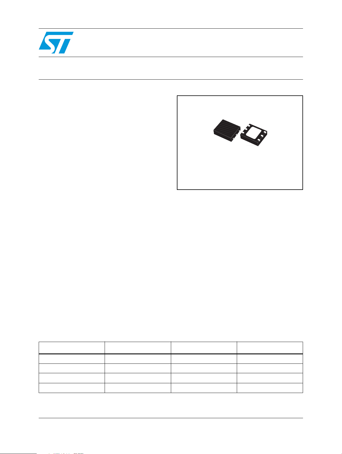
■ Available in DFN6D (3x3 mm) exposed pad
Description
DS(ON)
typ.150 mΩ
ST1S06xx
DFN6D (3x3 mm)
Besides, a low output ripple is guaranteed by the
current mode PWM topology and by the use of low
ESR SMD ceramic capacitors. The device is
thermal protected and current limited to prevent
damages due to accidental short circuit. The
ST1S06xx is available in DFN6D (3x3 mm)
package.
The ST1S06xx is a step down DC-DC converter
optimized for powering low-voltage digital core in
HDD applications and, generally, to replace the
high current linear solution when the power
dissipation may cause an high heating of the
application environment. It provides up to 1.5 A
over an input voltage range of 2.7 V to 6 V. An high
switching frequency (1.5 MHz) allows the use of
tiny surface-mount components: as well as the
resistor divider to set the output voltage value,
only an inductor and two capacitors are required.
Table 1. Device summary
Part numbers Marking Order codes Package
ST1S06 ST1S06 ST1S06PUR DFN6D (3 x 3 mm)
May 2009 Doc ID 12236 Rev 9 1/20
ST1S06A ST1S06A ST1S06APUR DFN6D (3 x 3 mm)
ST1S06XX12 1S0612 ST1S06PU12R DFN6D (3 x 3 mm)
ST1S06XX33 1S0633 ST1S06PU33R DFN6D (3 x 3 mm)
www.st.com
20

Contents ST1S06xx
Contents
1 Diagram . . . . . . . . . . . . . . . . . . . . . . . . . . . . . . . . . . . . . . . . . . . . . . . . . . . 3
2 Pin configuration . . . . . . . . . . . . . . . . . . . . . . . . . . . . . . . . . . . . . . . . . . . 4
3 Maximum ratings . . . . . . . . . . . . . . . . . . . . . . . . . . . . . . . . . . . . . . . . . . . . 5
4 Electrical characteristics . . . . . . . . . . . . . . . . . . . . . . . . . . . . . . . . . . . . . 6
5 Typical performance characteristics . . . . . . . . . . . . . . . . . . . . . . . . . . . . 9
6 Typical application . . . . . . . . . . . . . . . . . . . . . . . . . . . . . . . . . . . . . . . . . 13
7 Application notes . . . . . . . . . . . . . . . . . . . . . . . . . . . . . . . . . . . . . . . . . . 14
8 Package mechanical data . . . . . . . . . . . . . . . . . . . . . . . . . . . . . . . . . . . . 15
9 Revision history . . . . . . . . . . . . . . . . . . . . . . . . . . . . . . . . . . . . . . . . . . . 19
2/20 Doc ID 12236 Rev 9

ST1S06xx Diagram
1 Diagram
Figure 1. Schematic diagram
Doc ID 12236 Rev 9 3/20

Pin configuration ST1S06xx
2 Pin configuration
Figure 2. Pin configuration (top view)
ST1S06
* Pin 1 is VFB for ADJ version and VO for Fixed version
Table 2. Pin description
Pin n° Symbol Note
1FB/V
2 GND System ground
3 SW Switching pin
4V
5V
6V
IN_SW
IN_A
INH
Feedback voltage / output voltage
O
Power supply for the mosfet switch
Power supply for analogic circuit
Inhibit pin to turn off the device
Exposed pad to be connected to GND
ST1S06A
4/20 Doc ID 12236 Rev 9

ST1S06xx Maximum ratings
3 Maximum ratings
Table 3. Absolute maximum ratings
Symbol Parameter Value Unit
V
IN_SW
V
IN_A
V
INH
SWITCH
voltage
VFB/V
V
O
T
J
T
STG
T
LEAD
Positive power supply voltage -0.3 to 7 V
Positive power supply voltage -0.3 to 7 V
Inhibit voltage -0.3 to VI + 0.3 V
Max. voltage of output pin -0.3 to 7 V
Feedback voltage -0.3 to 2.5 V
O
Output voltage (for VO > 1.6 V) -0.3 to 6 V
Max junction temperature -40 to 150 °C
Storage temperature range -65 to 150 °C
Lead temperature (soldering) 10 sec 260 °C
Note: Absolute maximum ratings are those values beyond which damage to the device may occur.
Functional operation under these conditions is not implied.
Table 4. Thermal data
Symbol Parameter Value Unit
R
R
thJA
thJC
Thermal resistance junction-ambient 55 °C/W
Thermal resistance junction-case 10 °C/W
Doc ID 12236 Rev 9 5/20

Electrical characteristics ST1S06xx
4 Electrical characteristics
V
125 °C unless otherwise specified. Typical values are referred to T
Table 5. Electrical characteristics for ST1S06
IN_SW
= V
IN_A
= V
= 5 V, VO = 1.2 V, CI = 4.7 µF, CO = 22 µF, L1 = 3.3 µH, TJ = -30 °C to
INH
= 25 °C.
J
Symbol Parameter Test conditions Min. Typ. Max. Unit
FB Feedback voltage 784 800 816 mV
I
FB
V
I
I
V
INH
VFB pin bias current 600 nA
Minimum input voltage IO = 10mA to 1.5A 2.7 V
I
V
> 1.2V 1.5 mA
Quiescent current
Q
Output current VI = 2.7 to 5.5V Note 1 1.5 A
O
Inhibit threshold
INH
< 0.4V, TJ = -30°C to 85°C 1 µA
V
INH
Device ON, V
= 2.7 to 5.5V 1.3
I
= 2.7 to 5V 1.2
I
Device OFF 0.4
I
INH
Inhibit pin current 2µA
%VO/ΔVIReference line regulation VI = 2.7V to 5.5V Note 1 0.2 0.3
%VO/ΔIOReference load regulation IO = 10mA to 1.5A Note 1 0.2 0.3
PWMfSPWM switching frequency VFB = 0.8V 1.2 1.5 1.8 MHz
%V
ΔV
%V
ΔI
VDevice ON, V
/
O
I
/
O
O
D
MAX
R
DSON
R
DSON
I
SWL
T
SHDN
T
HYS
%VO/ΔIOLoad transient response
%VO/ΔIOShort circuit removal response
Note: 1 Guaranteed by design, but not tested in production
Maximum duty cycle 80 87 %
-N NMOS switch on resistance ISW = 750 mA 0.12 Ω
-P PMOS switch on resistance ISW = 750 mA 0.15 Ω
Switching current limitation Note 1 2.3 A
I
= 10mA to 100mA, VO = 3.3V 65
ν
Efficiency Note 1
O
= 100mA to 1.5A, VO = 3.3V 85 90
I
O
Thermal shutdown 130 150 °C
Thermal shutdown hysteresis 15 °C
I
= 100mA to 750mA, TJ =
O
25°C t
I
T
= tF ≥ 200ns, Note 1
R
= 10mA to IO = short,
O
= 25°C Note 1
J
%
-5 +5 %V
-10 +10 %V
O
O
6/20 Doc ID 12236 Rev 9

ST1S06xx Electrical characteristics
V
125 °C unless otherwise specified. Typical values are referred to T
Table 6. Electrical characteristics for ST1S06PM12
IN_SW
= V
IN_A
= V
= 5 V, VO = 1.2 V, CI = 4.7 µF, CO = 22 µF, L1 = 3.3 µH, TJ = -30 °C to
INH
= 25 °C.
J
Symbol Parameter Test conditions Min. Typ. Max. Unit
OUT Output feedback pin 1.176 1.2 1.224 V
I
V
I
I
V
INH
IO pin bias current VO = 1.5V 15 20 µA
O
Minimum input voltage IO = 10mA to 1.5A 2.7 V
I
V
> 1.2V 1.5 mA
Quiescent current
Q
Output current VI = 2.7 to 5.5V Note 1 1.5 A
O
Inhibit threshold
INH
< 0.4V, TJ = -30°C to 85°C 1 µA
V
INH
Device ON, V
= 2.7 to 5.5V 1.3
I
= 2.7 to 5V 1.2
I
Device OFF 0.4
I
INH
Inhibit pin current 2µA
%VO/ΔVIReference line regulation VI = 2.7V to 5.5V Note 1 0.2 0.3
%VO/ΔIOReference load regulation IO = 10mA to 1.5A Note 1 0.2 0.3
PWMfSPWM switching frequency VFB = 0.8V 1.2 1.5 1.8 MHz
D
MAX
R
DSON
R
DSON
I
SWL
T
SHDN
T
HYS
%VO/ΔIOLoad transient response
Maximum duty cycle 80 87 %
-N NMOS switch on resistance ISW = 750 mA 0.12 Ω
-P PMOS switch on resistance ISW = 750 mA 0.15 Ω
Switching current limitation Note 1 2.3 A
I
= 10mA to 100mA, VO = 1.2V 60
ν
Efficiency Note 1
O
= 100mA to 1.5A, VO = 1.2V 80 85
I
O
Thermal shutdown 130 150 °C
Thermal shutdown hysteresis 15 °C
I
= 100mA to 750mA, TJ =
O
25°C tR = tF ≥ 200ns, Note 1
-5 +5 %V
%V
ΔV
%V
ΔI
%
VDevice ON, V
/
O
I
/
O
O
O
I
= 10mA to IO = short,
%VO/ΔIOShort circuit removal response
O
= 25°C Note 1
T
J
Note: 1 Guaranteed by design, but not tested in production
Doc ID 12236 Rev 9 7/20
-10 +10 %V
O
 Loading...