

Page 1
SPWF04SA
SPWF04SC
Serial-to-Wi-Fi b/g/n intelligent modules
Features
2.4 GHz IEEE 802.11 b/g/n transceiver
STM32 ARM Cortex-M4, with 256 KB RAM
and
2 M
B Flash memory
Integrated TCP/IP protocol stack
–
2 (TBC) simultaneous TCP or UDP
clients and 2 (TBC) socket server
–
supporting up to TLS 1.2, including
common encryption algorithms: AES
(128, 256), hash (MD5, SHA-1, SHA-
256) and public key algorithms (RSA,
ECC)
–
Web server supporting dynamic web pages
WEP/WPA/WPA2 personal and enterprice
security
System modes: Station, IBSS, and miniAP
miniAP easily provisioned (SSID, PWD)
Fast Wi-Fi reassociation after reset
Firmware update via UART and Over The Air
(FOTA
TX power
–
18.3 dBm @ 1 Mbps DSSS
–
13.7 dBm @ 54 Mbps OFDM
RX sensitivity
–
-96.0 dBm @ 1 Mbps DSSS
–
-74.5 dBm @ 54 Mbps OFDM
16 configurable GPIOs available
UART and SPI interface to host system
Advanced low-power modes
–
Standby with RTC: 0.8mA (TBC)
–
Sleep connected (DTIM=1): 19 mA
–
RX traffic 113 mA typical
–
TX traffic 248 mA typical @ 18 dBm
Simple AT command set host interface through
UART
Small form factor: 26.92 x 15.24 x 2.35 mm
Single voltage supply (3.3 V typical)
Multiple antenna options:
–
Integrated antenna (SPWF04SA
versions)
–
Integrated u.fl connector (SPWF04SC
versions)
Industrial temperature range: -40 °C to 85 °C
FCC/CE/IC/SRRC certified
RoHS compliant
Surface mount PCB module
Applications
Smart appliances
Industrial control and data acquisition
Home automation and security systems
Wireless sensors
Cable replacement
Medical equipment
Machine-to-machine communication
April 2016 DocID025635 Rev 7 1/18
.
Preliminary Datasheet
www.st.com
Page 2

Description
SPWF04SA, SPWF04SC
2/18
DocID025635 Rev 7
1
Description
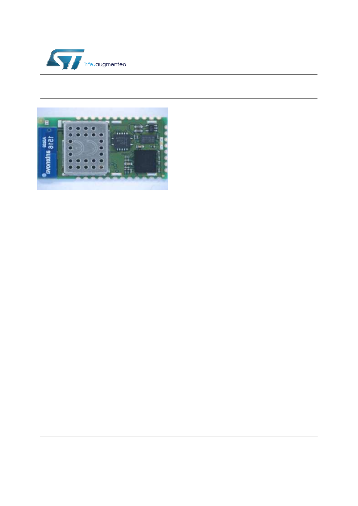
The SPWF04SA and the SPWF04SC intelligent Wi-Fi modules represent a plug-and-play
and standalone 802.11 b/g/n solution for easy integration of wireless Internet connectivity
features into existing or new products.
Configured around a single-chip 802.11 transceiver with integrated PA and comprehensive
power management subsystem, and an STM32 microcontroller with an extensive GPIO
suite, the modules also incorporate timing clocks and voltage regulators. Two different
options exist based on the integrated Flash memory.
The module is available either configured with an embedded micro 2.45 GHz highly-efficient
ISM band antenna (SPWF04SA), or with an u.fl connector for external antenna connection
(SPWF04SC).
With low power consumption and ultra-compact (2.7 x 1.5 cm) footprint, the modules are
ideal for fixed and mobile wireless applications, as well as challenging battery-operated
applications.
The SPWF04Sx parts are released with an integrated full featured TCP/IP protocol stack
with added web server and additional application service capabilities, such as REST API for
accessing files on servers in the cloud and support for dynamic web pages with CGI/SSI
functions to easily interact with the module and the host processor over the air.
For secure end-to-end communication with the cloud, an SSL/TLS stack is embedded in
every module with no licensing charge. See application note AN4683 (TBC) for details.
The SW package also includes an AT command layer interface for user-friendly access to
the stack functionalities via the UART serial port. For details, see user manual UM1695
(TBC).
It is always possible to upgrade the module firmware via UART and Over The Air (FOTA).
Inside of the 2 MB extended Flash available on the SPWF04S module, 1 MB of the Flash is
dedicated to FW upgrade and to host proprietary files, organized in a file system image,
accessible through the integrated web server.
FOTA is also possible with the SPWF04Sx module.
ST may update the FW provided with the modules at any time. ST recommends that users
regularly check for documentation and the current FW version available at
www.st.com/wifimodules.
Page 3

SPWF04SA, SPWF04SC
Description
Figure 1. Block diagram
DocID025635 Rev 7 3/18
Page 4

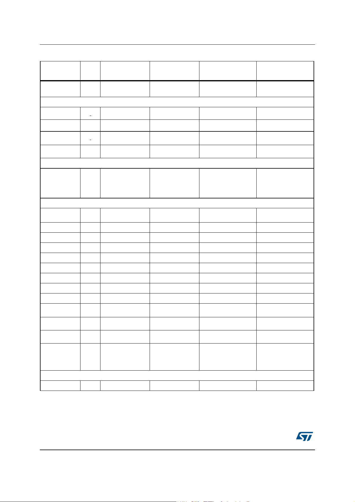
General electrical specifications
SPWF04SA, SPWF04SC
Parameter
Test condition/comment
Min.
Typ.
Max.
Unit
Voltage supply
-
-0.3
-
4.0
V
Vin for 5 V tolerant pins
-0.3
5.5
V
Vin for all other pins
-0.3
3.6
V
Storage temperature range
-55
105
°C
Parameter
Test condition/comment
Min.
Typ.
Max.
Unit
Operating temperature range
Industrial
-40 85
°C
3.3 V
supply
Input supply voltage
3.3 V supply input
3.1
3.3
3.6
V
Standby
Both the STM32 and the radio
are in standby power states
0.8
mA
Sleep
The STM32 is in stop power
state and the radio is in sleep
power state
19
mA
Low power state
The STM32 is active and the
radio is in sleep power state
52
mA
TX
802.11b
TX power=0 dBm
236 mA
TX power=10 dBm
250 mA
TX power=18 dBm
344 mA
802.11g
TX power=0 dBm
210 mA
TX power=10 dBm
243 mA
TX power=18 dBm
338 mA
RX
802.11b
105 mA
802.11g
105 mA
2
General electrical specifications
Table 2. Operating conditions and input power specifications
Table 1. Absolute maximum ratings
(1)
1.
Typical results are at room temperature only.
4/18 DocID025635 Rev 7
Page 5

SPWF04SA, SPWF04SC
Digital interface specifications
Parameter
Test condition/comment
Min.
Typ.
Max.
Unit
Inputs
VIH
2.3
-
3.6
V
VIL
0
0.9
V
Outputs
VOH
IOH=4 mA
2.4
3.6
V
VOL
IOL=4 mA
0
0.4
V
3
Digital interface specifications
Table 3. Digital interface specifications, I/O pins
DocID025635 Rev 7 5/18
Page 6

RF characteristics
SPWF04SA, SPWF04SC
Parameter
Test condition/comment
Min.
Typ.
Max.
Unit
11b, 1 Mbps
-96 dBm
RX sensitivity
(1)
11b, 2 Mbps
-93 dBm
11b, 5.5 Mbps
-91 dBm
11b, 11 Mbps
-87 dBm
11g, 9 Mbps
-89.5
dBm
11g, 18 Mbps
-86 dBm
11g, 36 Mbps
-80 dBm
11g, 54 Mbps
-74.5
dBm
11n, MCS1, 13 Mbps
-86.5
dBm
11n, MCS3, 26 Mbps
-81.5
dBm
11n, MCS5, 52 Mbps
-74 dBm
11n, MCS7, 65 Mbps
-71 dBm
Channel-to-channel
de-sensitivity
CH1 to 14
11g, 54 Mbps, 10%PER
1
dB
Maximum input signal
CH7
11g, 54 Mbps
-20 dBm
Adjacent channel rejection
11Mbps
38 dBc
9 Mbps
20 dBc
54 Mbps
4
dBc
MCS1
24 dBc
MCS7
3
dBc
TX output power
(1)
11b, 1 Mbps
@ 11b spectral mask
18.3
dBm
11b, 11 Mbps
18.3 dBm
11g, 9 Mbps
@ 11g spectral mask
18.3 dBm
11g, 54 Mbps
EVM = -27 dB, 4.5%
13.7 dBm
11n, MCS1
@ 11n spectral mask
18.3 dBm
11n, MCS7
EVM = -27 dB
13.5 dBm
On-board antenna gain
Average
-1.2 dBi
External antenna gain
SG901-1066 average
including cable loss
2.8
dBi
4
RF characteristics
Table 4. RF characteristics
1. Output power and sensitivities are measured with a 50 Ω connection at the antenna port.
6/18 DocID025635 Rev 7
Page 7

SPWF04SA, SPWF04SC
Pinout description
Signal name
Type Pin number
Main function
Alternate
functions
(1)
Notes
GPIO - general purpose input/output
GPIO[0]
I/O
16
General purpose
input/output Restore to
factory
settings
(2)
Input pull down and
5V tolerant
GPIO[1]
I/O 17
General purpose
input/output/ADC
Input pull down and
5V tolerant
GPIO[2]
I/O 19
General purpose
input/output/PWM
Floating and 5V
tolerant
GPIO[3]
I/O 1
General purpose
input/output
Input pull down and
5V tolerant
GPIO[6]
I/O
22
General purpose
input/output Wake
Up/Sleep
Inhibit
(3)
Input pull down and
5V tolerant
GPIO[4]
I/O 18
General purpose
input/output
GPIO[5]
I/O 20
General purpose
input/output
GPIO[7]
I/O
13
General purpose
input/output STA/Mini
AP
Switch/WPS
Pushbutton
(4)
GPIO[8]
I/O 4
General purpose
input/output
GPIO[9]
I/O 7
General purpose
input/output/SPI
nHostInterrupt
GPIO[11]
I/O
11
GPIO[12]
I/O 12
General purpose
input/output
GPIO[15]
I/O 21
General purpose
input/output/DAC
Monitoring purpose with no alternate function
GPIO[10]
I/O 5
Drives LED, Blinks while
running
GPIO[13]
I/O 15
Drives LED, Wi-Fi link
up
5
Pinout description
Table 5. Pinout description
DocID025635 Rev 7 7/18
Page 8
Pinout description
SPWF04SA, SPWF04SC
Signal name
Type Pin number
Main function
Alternate
functions
(1)
Notes
GPIO[14]
I/O 14
LED drive, Power
up
UART pins
RXD /
MOSI
I
8
5V tolerant
TXD /
MISO
6
5V Tolerant
CTS / nCS
I
9
Active low, 5V tolerant
RTS / CLK
O
10
5V tolerant
Reset
RESETn
I
3
Reset input
Active low for 5 ms
with pull up to
2.5VDC. Not 5V
tolerant
Supply pins and paddle
3.3 V
24
Voltage supply
Decouple with 10uF
capacitor
Ground 23
Ground
LSE 34
HSE 35
SWD I/O 26
SWD CLK
29
GPIO16 27
Not available
GPIO17 28
Not available
GPIO18 30
Not available
SDIO CLK /
SPI CLK
31
SDIO D0 /
SPI MISO
32
SDIO CMD
/ SPI MOSI
33
Ground Paddle
25
Ground
Add plenty of ground
vias for thermal
dissipation and ground
return
Boot loader
BOOT0 I 2
Boot loader
(5)
Table 5. Pinout description (continued)
1.
The activation of ALT function depends upon the firmware version or upon the variable configuration.
2.
To perform the factory reset of the variables, pin GPIO0 must be high during powerup.
3.
GPIO function running when low power mode variable is enabled.
4.
Introduced with the release 3.0 of AT Full stack. To enable the STAToMiniAP switch the GPIO[7] needs to be put low
together with the HW reset
8/18 DocID025635 Rev 7
Page 9

SPWF04SA, SPWF04SC
Pinout description
5.
To enable the firmware download, pin BOOT0 needs to be high during power up. RESETn need to be pulled low at least 5
ms to initiate the firmware download sequence.
Application guidelines
The HOST processor should control the RESETn pin of the module in order to recover from unexpected
behavior using the HW reset.
DocID025635 Rev 7 9/18
Page 10

Module reflow
SPWF04SA, SPWF04SC
Profile feature
PB-free assembly
Average ramp-up rate (T
SMAX
to TP)
3 °C/sec max
Preheat:
– Temperature min. (Ts min.)
– Temperature max. (Ts max.)
– Time (Ts min. to Ts max) (ts)
150 °C
200 °C
60-100 sec
Critical zone:
Temperature T
L
Time T
L
217 °C
60-70 sec
Peak temperature (TP)
240 + 0 °C
Time within 5 °C of actual peak temperature (TP)
10-20 sec
Ramp-down rate
6 °C/sec
Time from 25 °C to peak temperature
8 minutes max.
6
Module reflow
The SPWF04SA and SPWF04SC are surface mount modules with a 6-layer PCB. The
recommended final assembly reflow profiles are indicated below.
The soldering phase must be executed with care: in order to prevent an undesired melting
phenomenon, particular attention must be paid to the setup of the peak temperature.
The following are some suggestions for the temperature profile based on the IPC/JEDEC JSTD-020C, July 2004 recommendations.
Table 6. Soldering values
Figure 2. Soldering profile
10/18 DocID025635 Rev 7
AM17477v1
Page 11

SPWF04SA, SPWF04SC
Regulatory compliance
Comment
FCC ID
S9NSPWFS04
On board antenna and external ANTENOVA TITANIS with connector version
IC ID
8976C-SPWFS04
On board antenna and external ANTENOVA TITANIS with connector version
ETSI
Compliant
Approved with on board antenna and connector version
7
Regulatory compliance
RF compliance
The RF certifications obtained are described in Table 7 below.
Table 7. RF certification summary
This radio transmitter IC ID 8976-SPWFS04 has been approved by Industry Canada to operate
with the antenna types listed below with the maximum permissible gain indicated.
Antenna types not included in this list, having a gain greater than the maximum gain indicated
for that type, are strictly prohibited for use with this device.
Note: The TITANIS antenna from ANTENOVA. is the only approved antenna using the u.fl
connector version.
Page 12

SPWF04SA, SPWF04SC
Regulatory compliance
*Note all data provided in this table are based on the Antenova reference board
FCC and IC
This module has been tested and complies with the FCC part 15 and IC RSS-247
regulations. These limits are designed to provide reasonable protection against harmful
interference in approved installations. This equipment generates, uses, and can radiate
radio frequency energy and, if not installed and used in accordance with the instructions,
may cause harmful interference to radio communications.
However, there is no guarantee that interference will not occur in a particular installation.
This device complies with part 15 of the FCC rules. Operation is subject to the following two
conditions:
1.
The device must not cause harmful interference.
and
2.
The device must accept any interference received, including interference that may
cause undesired operation.
Modifications or changes to this equipment not expressly approved by the party responsible
for compliance may render void the user's authority to operate this equipment.
The safe user distance, for RF Exposure, is ≥ 50mm (in compliance with 447498 D01
General RF Exposure Guidance v06 and RSS-102 Issue 5).
Modular approval, FCC and IC
- FCC ID: S9NSPWFS04
- IC: 8976C-SPWFS04
In accordance with FCC part 15, the modules SPWF04SA and SPWF04SC are listed above
as a modular transmitter device.
DocID025635 Rev 7 11/18
Page 13

Regulatory compliance
SPWF04SA, SPWF04SC
Labeling instructions
When integrating the SPWF04SA and SPWF04SC into the final product, it must be ensured
that the FCC and IC labeling requirements specified below are satisfied. Based on the
Public Notice from FCC, the product into which the ST transmitter module is installed must
display a label referring to the enclosed module. The label should use wording like the
following:
Contains Transmitter Module
- FCC ID: S9NSPWFS04
- IC: 8976C-SPWFS04
Any similar wording that expresses the same meaning may also be used.
CE
This module complies with the following European EMI/EMC and safety directives and
standards:
– ETSI EN 300 328 V1.8.1:2012
– EN 301 489-1 V1.9.2:2011 + EN 301 489-17 V2.2.1:2009
– EN 60950-1:2006 + A11:2009 + A1:2010 + A12:2011 + A2:2013
– EN 62479:2010
Figure 3. CE certified
SRRC
(See the A.1 at the bottom of this document for the French translation)
12/18 DocID025635 Rev 7
(T.B.C.)
The SPWF04Sx module complies with Chinese SRRC certification.
– SRRC CMIIT ID: (T.B.D.)
Page 14

SPWF04SA, SPWF04SC
Package information
8
Package information
In order to meet environmental requirements, ST offers these devices in different grades of
ECOPACK® packages, depending on their level of environmental compliance. ECOPACK
specifications, grade definitions and product status are available at: www.st.com.
ECOPACK® is an ST trademark.
Figure 4. Top view of the module shield
®
Shield
CE Logo
Figure 5. Bottom view of the module
Data Matrix
Model Series Name
zone
Board Design Reference
FCC and IC ID zone
DocID025635 Rev 7 13/18
Page 15

Package information
SPWF04SA, SPWF04SC
Figure 6. Wi-Fi module dimensions
Note: An antenna area of 217 x 520 mils must be free of any ground metalization or traces under
the unit. The area extending away from the antenna should be free from metal on the PCB
and housing to meet expected performance levels. Pin 25 is the required paddle ground and
is not shown in this diagram.
14/18 DocID025635 Rev 7
Page 16

SPWF04SA, SPWF04SC
Package information
Figure 7. Wi-Fi module footprint
PCB design requires a detailed review of the center exposed pad. This pad requires good
thermal conductivity. Soldering coverage should be maximized and checked via x-ray for
proper design. There is a trade-off between providing enough soldering for conductivity and
applying too much, which allows the module to “float” on the paddle creating reliability
issues. ST recommends two approaches, a large center via that allows excess solder to
flow down into the host PCB with smaller vias around it, or many smaller vias with just
enough space for the viscosity of the chosen solder/flux to allow some solder to flow into the
smaller vias.
Either of these approaches must result in 60% or more full contact solder coverage on the
paddle after reflow. ST strongly encourages PCB layout teams to work with their EMS
providers to ensure vias and solder paste designs that will result in satisfactory
performance.
DocID025635 Rev 7 15/18
Page 17

Regulatory compliance
SPWF04SA/C
Order codes
Description
SPWF04SA
Wi-Fi module with integrated antenna, 1 MB of Flash and Wi-Fi full stack
SPWF04SC
Wi-Fi module with integrated ufl connector, 1 MB of Flash and Wi-Fi full stack
9
Ordering information
Table 8. Ordering information
Note: Refer to the user manual for a complete list of features and commands available in the Wi-Fi
full stack.
Page 18

Regulatory compliance
SPWF04SA/C
Déclaration de conformité
A.1 Certification FCC
Le module SPWF04SA/C a été testé et déclaré conforme avec la section 15 de la
Règlementation FCC. Ces limitations sont stipulées afin de procurer une protection
raisonnable contre les interférences gênantes dans les installations approuvées. Cet
appareil génère, utilise et diffuse des ondes radio et, s’il n’est pas installé et utilisé en
conformité avec les instructions dont il fait l’objet, peut causer des interférences gênantes
sur les communications radio.
Il n’y a cependant pas de garantie qu’une interférence ne se produira pas dans une
installation particulière.
Cet appareil est en conformité avec la section 15 des règlements FCC. L’utilisation est
soumise aux deux conditions suivantes: (1) cet appareil ne doit pas causer
d'interférences nocives, et (2) Cet appareil doit supporter toute interférence reçue, y
A.1.1 Instructions d'étiquetage
A1 DocID temporary Rev1
compris des interférences qui peuvent provoquer un fonctionnement non désiré.
Tout changement ou modification fait(e) à cet appareil et non expressément
approuvé(e) par STMicroelectronics peut annuler l’autorisation pour l’utilisateur de faire
fonctionner l’appareil.
Approbation du module
FCC ID: S9NSPWFS04
Conformément à la section 15 des règlements FCC, le module SPWF04SA/C est répertorié
comme un dispositif émetteur modulaire.
Ce module n’est évalué que pour une utilisation autonome. Les produits finis incorporant
plusieurs émetteurs doivent être conformes à la colocation et aux exigences d'exposition
RF en concordance avec les procédures FCC multi-émetteurs. D’autres émetteurs
fonctionnant dans des dispositifs portables exposés aux RF (par exemple, situés à moins
de 20 cm des personnes avec dispositifs portatifs ou portés contre le corps) peuvent
nécessiter d'une approbation séparée.
Lors de l'intégration du module SPWF04SA/C dans le produit final, le fabricant doit
s’assurer que les exigences en matière d'étiquetage de la FCC sont satisfaites . Une
déclaration doit être placée sur l’étiquette extérieure du produit final indiquant que le
produit comprend un module certifié. L'étiquette doit comporter les informations suivantes
(ou une mention analogue que recouvre la même notion):
Contient FCC ID: S
OU
Ce produit contient FCC ID: S9NSPWFS04
Le sous-traitant doit inclure les énoncés suivants sur l’étiquette extérieure du produit final
à moins que le produit ne soit trop petit (par exemple moins de 4 x 4 pouces):
Cet appareil est en conformité avec la section 15 des règlements FCC. L’utilisation est
soumise aux deux conditions suivantes:
(1) cet appareil ne doit pas causer d'interférences nocives, et
(2) Cet appareil doit supporter toute interférence reçue, y compris des interférences qui
peuvent provoquer un fonctionnement non désiré.
9NSPWFS04
Page 19

Regulatory compliance
SPWF04SA, SPWF04SC
A.1.2 Instructions pour l’utilisation du produit
La présente section concerne les produits finis contenant le module SPWF04SA/C,
assujettis aux normes FCC. Le manuel du produit final doit contenir la déclaration
suivante (ou une mention analogue que recouvre la même notion):
“ Avertissement: Les changements ou modifications non expressément approuvés par
la partie responsable de la conformité pourraient annuler l'autorisation de l'utilisateur
de faire fonctionner cet équipement. (Section 15.21)”
Dans le cas où le produit finis d’un fabriquant OEM rentre dans les limites de la
Classe B (résidentiel), les énoncés suivants doivent être inclus dans le manuel du
produit finis:
“Remarque : Cet équipement a été testé et déclaré conforme aux limitations prévues dans
le cadre de la classe B des appareils numériques, définies par la section 15 du règlement
de la FCC. Ces limites sont conçues pour fournir une protection raisonnable contre toute
interférence dangereuse issue d'une installation résidentielle. Cet équipement produit,
utilise et peut émettre de l'énergie radio électrique et, s'il n'est pas installé et utilisé
conformément aux présentes instructions, peut causer des interférences nuisibles aux
communications radio. Cependant, il se peut que des interférences se produisent dans
une installation particulière. Si cet appareil cause des interférences nuisibles à la
réception des signaux de radio ou de télévision, ce qui peut être déterminé en allumant et
en éteignant l'appareil, on encourage l'utilisateur d'essayer de corriger ces interférences
par l'un des moyens suivants:
– Réorienter ou repositionner l'antenne de réception.
– Augmenter la distance séparant l’équipement du récepteur.
– Connecter l’équipement à une prise appartenant à un circuit différent de celui
sur lequel le récepteur est connecté.
– Consulter le revendeur ou un technicien radio/TV expérimenté pour obtenir de
l’aide.”
Dans le cas où le produit fini d’un sous-traitant rentre dans les limites imposées aux
appareils numériques de classe A, les énoncés suivants doivent être inclus dans le
manuel du produit finis:
“REMARQUE : Cet appareil a été testé et certifié conforme aux spécifications d'un
appareil électronique de classe A (class A digital device), conformément à la partie 15 du
règlement de la FCC. Ces contraintes sont destinées à fournir une protection raisonnable
contre les interférences nuisibles quand l'appareil est utilisé dans une installation
commerciale. Cet équipement produit, utilise et peut émettre de l'énergie radio électrique
et, s'il n'est pas installé et utilisé conformément aux présentes instructions, peut causer
des interférences nuisibles aux communications radio. L'utilisation de cet appareil dans
une installation résidentielle peut entraîner des interférences nuisibles et l'utilisateur devra
corriger les interférences à ses propres frais.”
Page 20

Regulatory compliance
SPWF04SA, SPWF04SC
A.2 Certification IC
Le module SPWF04SA/C a été testé et déclaré conforme avec la Règlementation IC
CNR-210. Ces limitations sont stipulées afin de procurer une protection raisonnable
contre les interférences gênantes en installations approuvées. Cet appareil génère, utilise
et diffuse des ondes radio et, s’il n’est pas installé et utilisé en conformité avec les
instructions dont il fait l’objet, peut causer des interférences gênantes sur les
communications radio.
Il n’y a cependant pas de garantie qu’une interférence ne se produira pas dans une
installation particulière.
A.2.1 Instructions d'étiquetage
Ce produit répond aux exigences de la norme CNR-210 d'Industrie Canada. Son
fonctionnement est soumis aux deux conditions suivantes:
(1) cet appareil ne doit pas causer d'interférences nocives, et
(2) Cet appareil doit supporter toute interférence reçue, y compris des interférences qui
peuvent provoquer un fonctionnement non désiré.
Tout changement ou modification fait(e) à cet appareil et non expressément
approuvé(e) par STMicroelectronics peut annuler l’autorisation pour l’utilisateur de faire
fonctionner l’appareil.
Approbation du module
IC: 8976C-SPWFS04
Conformément à IC CNR-210, le module SPWF04SA/C est répertorié comme un dispositif
émetteur modulaire
Ce module n’est évalué que pour une utilisation autonome. Les produits finis incorporant
plusieurs émetteurs doivent être conformes à la colocation et aux exigences d'exposition
RF en concordance avec les procédures FCC multi-émetteurs. D’autres émetteurs
fonctionnant dans des dispositifs portables exposés aux RF (par exemple, situés à moins
de 20 cm des personnes avec dispositifs portatifs ou portés contre le corps) peuvent
nécessiter d'une approbation séparée.
Lors de l'intégration du module SPWF04SA/C dans le produit final, le fabricant doit
s’assurer que les exigences en matière d'étiquetage de la IC sont satisfaites . Une
déclaration doit être placée sur l’étiquette extérieure du produit final indiquant que le
produit comprend un module certifié. L'étiquette doit comporter les informations suivantes
(ou une mention analogue que recouvre la même notion):
OU
Le sous-traitant doit inclure les énoncés suivants sur l’étiquette extérieure du produit final
à moins que le produit ne soit trop petit (par exemple moins de 4 x 4 pouces):
Cet appareil est en conformité aux normes IC. L’utilisation est soumise aux deux
conditions suivantes:
(1) cet appareil ne doit pas causer d'interférences nocives, et
(2) Cet appareil doit supporter toute interférence reçue, y compris des interférences qui
peuvent provoquer un fonctionnement non désiré
(a)
Contient IC ID: 8976C-SPWFS04
Ce produit contient
IC ID: 8976C-SPWFS04
Page 21

Regulatory compliance
SPWF04SA, SPWF04SC
A.2.2 Instructions pour l’utilisation du produit
La présente section concerne les produits finis contenant le module SPWF04SA/C,
assujettis aux normes IC. Le manuel du produit final doit contenir la déclaration suivante
(ou une mention analogue que recouvre la même notion):
“Avertissement: Les changements ou modifications non expressément approuvés par la
partie responsable de la conformité pourraient annuler l'autorisation de l'utilisateur de
faire fonctionner cet équipement. (CNR-210)”
Dans le cas où le produit finis d’un fabriquant OEM rentre dans les limites de la
Classe B (résidentiel), les énoncés suivants doivent être inclus dans le manuel du
produit finis:
“ Remarque : Cet équipement a été testé et déclaré conforme aux limitations prévues dans
le cadre de la classe B des appareils numériques, définies par la norme CNR-210
d'Industrie Canada.
Page 22

Regulatory compliance
SPWF04SA, SPWF04SC
Ces limites sont conçues pour fournir une protection raisonnable contre toute
interférence dangereuse issue d'une installation résidentielle. Cet équipement produit,
utilise et peut émettre de l'énergie radio électrique et, s'il n'est pas installé et utilisé
conformément aux présentes instructions, peut causer des interférences nuisibles aux
communications radio. Cependant, il se peut que des interférences se produisent dans
une installation particulière. Si cet appareil cause des interférences nuisibles à la
réception des signaux de radio ou de télévision, ce qui peut être déterminé en allumant et
en éteignant l'appareil, nous encourageons l'utilisateur à essayer de corriger ces
interférences par l'un des moyens suivants:
– Réorienter ou repositionner l'antenne de réception.
– Augmenter la distance séparant l’équipement du récepteur.
– Connecter l’équipement à une prise appartenant à un circuit différent de celui
sur lequel le récepteur est connecté.
– Consulter le revendeur ou un technicien radio/TV expérimenté pour obtenir de
l’aide.”
Dans le cas où le produit finis d’un fabriquant OEM rentre dans le cadre des limites
imposées aux appareils numériques de classe A, les énoncés suivants doivent être inclus
dans le manuel du produit finis:
“ REMARQUE: Cet appareil a été testé et certifié conforme aux spécifications d'un appareil
électronique de classe A (class A digital device), conformément à la norme CNR-210
d'Industrie Canada. Ces contraintes sont destinées à fournir une protection raisonnable
contre les interférences nuisibles quand l'appareil est utilisé dans une installation
commerciale. Cet équipement produit, utilise et peut émettre de l'énergie radio électrique
et, s'il n'est pas installé et utilisé conformément aux présentes instructions, peut causer
des interférences nuisibles aux communications radio. L'utilisation de cet appareil dans
une installation résidentielle peut entraîner des interférences nuisibles et l'utilisateur devra
corriger les interférences à ses propres frais.”
A.3 Certification CE
Le module SPWF04SA/C a obtenu une certification de conformité aux normes suivantes:
– EN 300 328 V1.8.1 :2012
– EN 300 328 V1.9.1 :2015
– EN 301 489-17 V2.2.1 :2009
– EN 301 489-1 V1.9.2:2011
– EN 62479 :2010
– EN60950-1:2006 + A11:2009 + A1:2010 + A12:2011 + A2 :2013
Le module est certifié CE:
Page 23

Regulatory compliance
SPWF04SA, SPWF04SC
A1
Page 24

SPWF04SA, SPWF04SC
Revision history
Date
Revision
Changes
27-Apr-2016
1
Initial release.
–
10
Revision history
Table 9. Document revision history
DocID025635 Rev 7 17/18
Page 25

SPWF04SA, SPWF04SC
STMicroelectronics NV and its subsidiaries (“ST”) reserve the right to make changes, corrections, enhancements, modifications, and
improvements to ST products and/or to this document at any time without notice. Purchasers should obtain the latest relevant information on
ST products before placing orders. ST products are sold pursuant to ST’s terms and conditions of sale in place at the time of order
acknowledgement.
Purchasers are solely responsible for the choice, selection, and use of ST products and ST assumes no liability for application assistance or
the design of Purchasers’ products.
No license, express or implied, to any intellectual property right is granted by ST herein.
Resale of ST products with provisions different from the information set forth herein shall void any warranty granted by ST for such product.
ST and the ST logo are trademarks of ST. All other product or service names are the property of their respective owners.
Information in this document supersedes and replaces information previously supplied in any prior versions of this document.
18/18 DocID025635 Rev 7
IMPORTANT NOTICE – PLEASE READ CAREFULLY
© 2016 STMicroelectronics – All rights reserved
 Loading...