

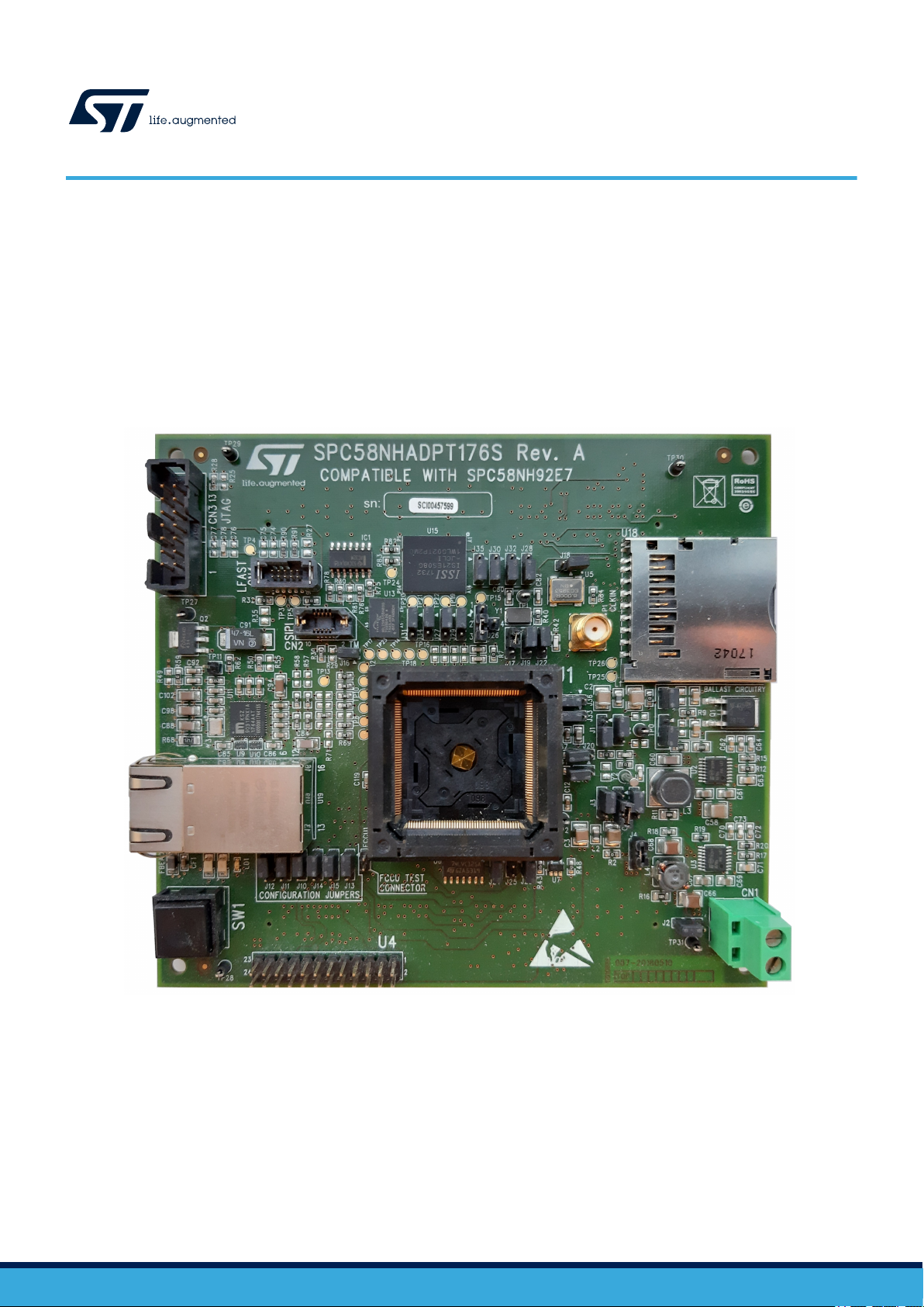
Note: picture not contractual
UM2731
User manual
SPC58NHADPT176S Rev.A evaluation board
Introduction
The SPC58NHADPT176S Rev.A evaluation board supports STMicroelectronics SPC58NH92 microcontroller in LQFP
24X24X1.4 176L.
Figure 1. SPC58NHADPT176S Rev.A
UM2731 - Rev 2 - April 2021
For further information contact your local STMicroelectronics sales office.
www.st.com

1 Overview
The SPC58NHADPT176S Rev. A mini module is an evaluation board supporting STMicroelectronics SPC58NH92
microcontroller in LQFP 24X24X1.4 176L package (LQFP 24X24X1.4 176L P0.5 EXPOSED PAD).
This mini module is designed to be connected onto the SPC58XXMB motherboard, offering a mechanism for easy
customer evaluation of the supported devices, and to facilitate hardware and software development.
The mini module may be used as a stand-alone unit allowing access to the CPU, but not access to the I/O pins
nor any motherboard peripherals.
1.1 Package contents
A SPC58NHADPT176S Rev. A adapter package includes the following items:
• SPC58NHADPT176S Rev. A mini module
1.2 Supported devices
The SPC58NHADPT176S Rev. A mini module supports the SPC58NH family in LQFP 24X24X1.4 176L package.
UM2731
Overview
UM2731 - Rev 2
page 2/37

UM2731
License agreement
2 License agreement
The packaging of this evaluation board was sealed with a seal stating, by breaking this seal, you agree to the
terms and conditions of the evaluation board license agreement, the terms and conditions of which are available
at:
https://www.st.com/resource/en/evaluation_board_terms_of_use/evaluationproductlicenseagreement.pdf
Upon breaking the seal, you and STMicroelectronics entered into the evaluation board license agreement, a copy
of which is also enclosed with the evaluation board for convenience.
Attention: This evaluation board only offers limited features for evaluating ST products. It has not been tested for use
with other products and is not suitable for any safety or other commercial or consumer application. This
evaluation board is otherwise provided “AS IS” and STMicroelectronics disclaims all warranties, express or
implied, including the implied warranties of merchantability and fitness for a particular purpose.
UM2731 - Rev 2
page 3/37

3 Handling precautions
Please take care to handle the package content in order to prevent electrostatic discharge.
Before the EVB is used or power is applied, please fully read the following sections on how to correctly configure
the board. Failure to correctly configure the board may cause irreparable component, MCU or EVB damage.
UM2731
Handling precautions
UM2731 - Rev 2
page 4/37

4 Hardware description
4.1 Hardware features
The SPC58NHADPT176S Rev. A mini module board has the following features:
• Connector for external power supplies input (5V) used in stand-alone mode
• Reset button with driver and led indicator
• Socket for device in LQFP 24X24X1.4 176L package
• Debug interfaces:
– 14-pin header connector for JTAG interface
– 10-pin header connector for JTAG/LFAST LVDS interface
– 10-pin header connector for SIPI interface
• 40 MHz crystal main oscillator with jumpers to optionally disconnect it
• 8 MHz oscillator with jumpers to optionally disconnect it
• Clock input through SMA connector with jumper to optionally disconnect it
• 2 X SAMTEC QSH series, 240-way connector to connect mini module to Motherboard
• 1 Gb/s Ethernet port
• HyperRAM and HyperFlash connected to HyperBUS interface
• Embedded eMMC device
• SD/MMC Card Reader
• 12x2 I/O connector
UM2731
Hardware description
UM2731 - Rev 2
page 5/37
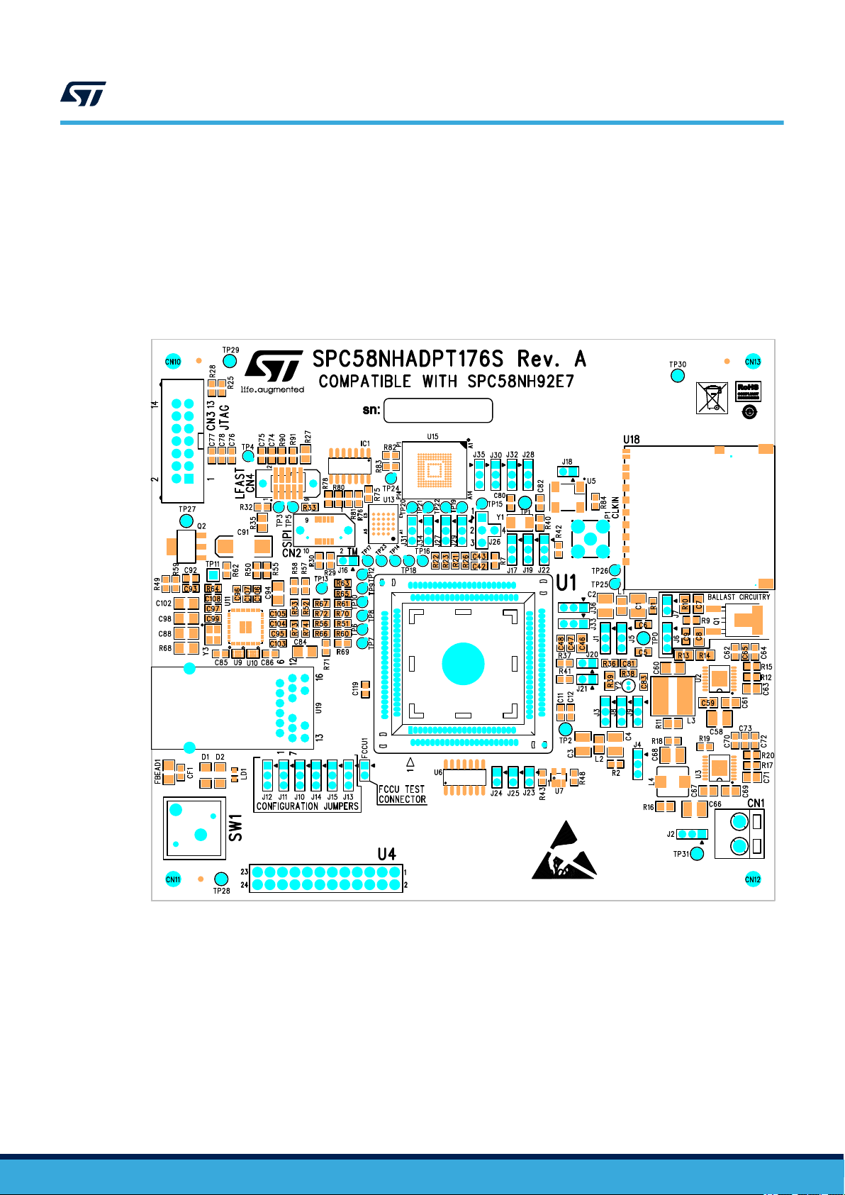
4.2 Hardware dimension
The mini module has the following dimensions:
• PCB area: 127 mm x 114.3 mm
• Top components height: 19 mm max
• Bottom components height: 3.5 mm max
• PCB thickness: 1.6 mm
Figure 2. SPC58NHADPT176S Rev. A top component view
UM2731
Hardware dimension
UM2731 - Rev 2
page 6/37
5 Power and system configuration
5.1 Power supplies
The mini module can be powered by providing voltages either supplied externally by the 2-Way PCB screw
connector (CN1) or supplied by the motherboard.
When the mini module is connected to the motherboard (MB), 3V3 and 5V0 are supplied by MB connector
selecting the associated jumpers. In this setup the external power supply input available on the mini module
MUST NOT BE USED.
When the SPC58NHADPT176S Rev. A mini module is used as a stand-alone board, 5V0 voltages must be
supplied externally, 3V3 and 1V2 voltages will be generated internally by specific circuit on the mini module.
The following jumpers are used to configure the power supply (common for all supported devices):
Table 1. Power configuration jumpers
Jumper Description Default Position
5.0V source for J3 pin1 (MB_5.0V_LR or 5.0
V_ADC) voltage configuration:
J1
• 1-2 MB_5.0V_LR
• 2-3 5.0 V_ADC
5.0V switching voltage configuration:
• 1-2 5 V EXT (external 5.0V supply)
J2
• 2-3 MB_5.0V_SR (5.0V from
Motherboard)
VDD_HV_ADR_S / VDD_HV_ADV voltage
configuration:
J3
• 1-2 5.0V source from J1 pin2
• 2-3 3.3 V_ADC source from J4 pin2
3V3 source (3.3V or MB_3.3V_SR) voltage
configuration:
J4
• 1-2 3.3V (3.3V from mini module)
• 2-3 MB_3.3V_SR
Main MCU supply (VDD_HV_IO_MAIN) voltage
configuration:
J5
• 1-2 5.0V_SR
• 2-3 3.3 V_SR from J4 pin2
Supply for BALLAST circuit configuration
J6
• 1-2 VDD_HV_IO_MAIN
• 2-3 5.0V_SR
BALLAST CIRCUIT ENABLE
J7
• Closed: enable
• Open: disable
VDD_LV voltage configuration:
J8
• 1-2 (1.2V_SR from J9 pin2)
• 2-3 (BALLAST circuit)
1.2V_SR switching configuration:
J9
• 1-2 MB_1.25V_SR (1.25V from MB)
• 2-3 1.2V (1.2V from mini module)
2-3
(5.0V_ADC)
2-3
(MB_5.0V_SR)
1-2
(5.0V_ADV)
1-2
(3.3V)
1-2
(5.0V_SR)
1-2
(VDD_HV_IO_MAIN)
Closed
(enable)
1-2
(1.2V_SR)
2-3
(1.2V from mini module)
UM2731
Power and system configuration
Figure 8. Overview of
SPC58NHADPT176S Rev. A mini
module - Top - C3
Figure 8. Overview of
SPC58NHADPT176S Rev. A mini
module - Top - D4
Figure 8. Overview of
SPC58NHADPT176S Rev. A mini
module - Top - C3
Figure 8. Overview of
SPC58NHADPT176S Rev. A mini
module - Top - D3
Figure 8. Overview of
SPC58NHADPT176S Rev. A mini
module - Top - D3
Figure 8. Overview of
SPC58NHADPT176S Rev. A mini
module - Top - D3
Figure 8. Overview of
SPC58NHADPT176S Rev. A mini
module - Top - D2
Figure 8. Overview of
SPC58NHADPT176S Rev. A mini
module - Top - C3
Figure 8. Overview of
SPC58NHADPT176S Rev. A mini
module - Top - D3
UM2731 - Rev 2
page 7/37
5.2 JTAG/LFAST LVDS interface configuration
The following jumpers need to configure the JTAG/LFAST LVDS/SIPI:
Table 2. JTAG/LFAST/SIPI Configuration jumpers
Jumper Description Default Position
SIPI pin 3 configuration
J10
• 1-2: RDY
• 2-3: PA14
TDI_LF configuration
J11
• 1-2: TDI_LF
• 2-3: PA8
TDO_LF configuration
J12
• 1-2: TDO_LF
• 2-3: PA9
JTAG pin 13 configuration
J13
• 1-2: EVTO
• 2-3: PJ3/PQ4
PC1 / ESR0
J14
• 1-2 ESR0
• 2-3 PC1
EVTO/ESR0
J15
• 1-2 ESR0
• 2-3 EVTO
1-2
(RDY)
1-2
(TDI_LF)
1-2
(TDO_LF)
1-2
(EVTO)
1-2
(ESR0)
1-2
(ESR0)
Figure 8. Overview of SPC58NHADPT176S Rev. A mini module - Top - A4
Figure 8. Overview of SPC58NHADPT176S Rev. A mini module - Top - A4
Figure 8. Overview of SPC58NHADPT176S Rev. A mini module - Top - A4
Figure 8. Overview of SPC58NHADPT176S Rev. A mini module - Top - B4
Figure 8. Overview of SPC58NHADPT176S Rev. A mini module - Top - B4
Figure 8. Overview of SPC58NHADPT176S Rev. A mini module - Top - B4
UM2731
JTAG/LFAST LVDS interface configuration
UM2731 - Rev 2
page 8/37
5.3 System clock configuration
The mini module supports the usage of crystal clock sources as well as external clock source:
Table 3. Clock configuration jumpers
Jumper Description Default Position
XTAL32 configuration
J20
• Close: connect pin 2 of 32.768 KHz crystal
(Y2) to XTAL32
EXTAL32 configuration
J21
• Close: connect pin 1 of 32.768 KHz crystal
(Y2) to EXTAL32
EXTAL configuration
• 1-2 connect pin 2 of 40 MHz crystal (Y1) to
J17
J19
J18
J22
EXTAL
• 2-3 connect EVB-EXTAL to EXTAL
XTAL configuration
• 1-2 connect pin 1 of 40 MHz crystal (Y1) to
XTAL
• 2-3 connect XTAL to GND
Enable 8 MHz oscillator power supply
• open - power off
• closed - power on
External 8 MHz clock source
• 1-2 OSC-MOD (from oscillator)
• 2-3 EXTAL-SMA (from SMA connector)
Open
Open
1-2
(Y1 pin2 to
EXTAL)
1-2
(Y1 pin1 to
XTAL)
Open
(power off)
1-2
(8 MHz from
oscillator)
UM2731
System clock configuration
Figure 8. Overview of SPC58NHADPT176S
Rev. A mini module - Top - C3
Figure 8. Overview of SPC58NHADPT176S
Rev. A mini module - Top - C3
Figure 8. Overview of SPC58NHADPT176S
Rev. A mini module - Top - C2
Figure 8. Overview of SPC58NHADPT176S
Rev. A mini module - Top - C2
Figure 8. Overview of SPC58NHADPT176S
Rev. A mini module - Top - C1
Figure 8. Overview of SPC58NHADPT176S
Rev. A mini module - Top - C2
5.4 Reset circuit
The mini module supports different ways to reset the microcontroller. To use and perform the reset driving there
are different jumpers and switches:
Jumper Description Default Position
SW1 Reset push button Open
Connect the external
J24
J23
J25
reset to the reset driver
for ESR0 and PORST
pins
Connect the external
reset to ESR0 pin
Connect the external
reset to PORST pin
Table 4. Reset configuration jumpers
Figure 8. Overview of SPC58NHADPT176S Rev. A
Close
Close
Close
Figure 8. Overview of SPC58NHADPT176S Rev. A
Figure 8. Overview of SPC58NHADPT176S Rev. A
Figure 8. Overview of SPC58NHADPT176S Rev. A
mini module - Top - A4
mini module - Top - C4
mini module - Top - C4
mini module - Top - C4
UM2731 - Rev 2
page 9/37
5.5 Other Jumpers
Table 5. Other jumpers
Jumper Description Default Position
J16 TESTMODE settings
Close
(10 KΩ down)
Figure 8. Overview of SPC58NHADPT176S Rev. A
mini module - Top - B2
5.6 Configuration for pin shared between HyperBus & eMMC
The jumpers described into the following table allow you to configure the pins shared between HyperBus and
eMMC.
Table 6. Pin shared between HyperBus & eMMC jumper
Jumper Description Default configuration Position
Data4 - PF9 configuration
J27
J29
J31
J34
• 1-2 DQ4_HB
(HyperBus)
• 2-3 D4_eMM
(eMMC)
Data5 – PF10
configuration
• 1-2 DQ5_HB
(HyperBus)
• 2-3 D5_eMM
(eMMC)
Data6 - PF11
configuration
• 1-2 DQ6_HB
(HyperBus)
• 2-3 D6_eMM
(eMMC)
Data7 - PF12
configuration
• 1-2 DQ7_HB
(HyperBus)
• 2-3 D7_eMM
(eMMC)
1-2
(HyperBus)
1-2
(HyperBus)
1-2
(HyperBus)
1-2
(HyperBus)
Figure 8. Overview of SPC58NHADPT176S Rev. A
mini module - Top - B2
Figure 8. Overview of SPC58NHADPT176S Rev. A
mini module - Top - B2
Figure 8. Overview of SPC58NHADPT176S Rev. A
mini module - Top - B2
Figure 8. Overview of SPC58NHADPT176S Rev. A
mini module - Top - B2
UM2731
Other Jumpers
UM2731 - Rev 2
page 10/37
Configuration for pin shared between eMMC & SD-card reader
5.7 Configuration for pin shared between eMMC & SD-card reader
The jumpers described into the following table allow you to configure the pins shared between SD-CARD
READER and eMMC.
Table 7. Pin shared between eMMC & SD-card reader jumper
Jumper Description Default configuration Position
Data1 - PJ4 configuration
J30
J32
J35
J28
J33
J36
• 1-2 D1_SD (SDCARD)
• 2-3 D1_eMM
(eMMC)
Data2 - PH5 configuration
• 1-2 D2_SD (SDCARD)
• 2-3 D2_eMM
(eMMC)
Data3 - PH6 configuration
• 1-2 D3_SD (SDCARD)
• 2-3 D3_eMM
(eMMC)
CLK - PJ2 configuration
• 1-2 CLK_SD (SDCARD)
• 2-3 CLK_eMM
(eMMC)
FBCLK - PJ0
configuration
• 1-2 FBCLK_SD
(SD-CARD)
• 2-3 FBCLK_eMM
(eMMC)
CMD - PJ1 configuration
• 1-2 CMD_SD (SDCARD)
• 2-3 CMD_eMM
(eMMC)
1-2
(SD-CARD)
1-2
(SD-CARD)
1-2
(SD-CARD)
1-2
(SD-CARD)
1-2
(SD-CARD)
1-2
(SD-CARD)
Figure 8. Overview of SPC58NHADPT176S Rev. A
mini module - Top - C1/C2
Figure 8. Overview of SPC58NHADPT176S Rev. A
mini module - Top - C1/C2
Figure 8. Overview of SPC58NHADPT176S Rev. A
mini module - Top - C1/C2
Figure 8. Overview of SPC58NHADPT176S Rev. A
mini module - Top - C1/C2
Figure 8. Overview of SPC58NHADPT176S Rev. A
mini module - Top - C2/C3
Figure 8. Overview of SPC58NHADPT176S Rev. A
mini module - Top - C2
UM2731
UM2731 - Rev 2
page 11/37
6 Hardware description
U9
HSP061-4M10Y
I/0 1
1
I/0 2
2
GND
3
I/0 3
4
I/0 45NC1
6
NC2
7
GND
8
NC3
9
NC4
10
TXRXM_B
TXRXP_B
GND GND
TXRXM_A
TXRXP_A TXRXP_A
TXRXP_B
TXRXM_B
TXRXM_A
U10
HSP061-4M10Y
I/0 1
1
I/0 2
2
GND
3
I/0 3
4
I/0 45NC1
6
NC2
7
GND
8
NC3
9
NC4
10
GND GND
TXRXM_D
TXRXP_D
TXRXM_C
TXRXP_C
TXRXM_D
TXRXP_C
TXRXM_C
TXRXP_D
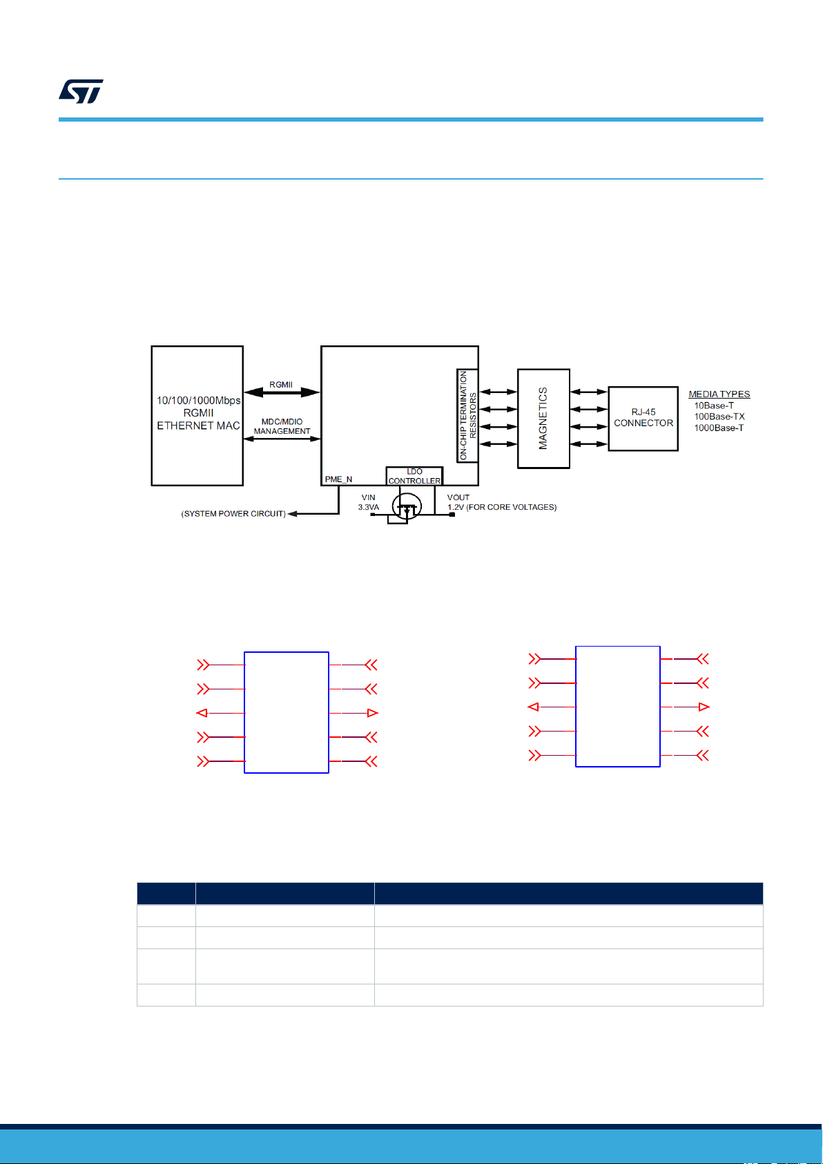
6.1 1 Gb/s ethernet interface
This paragraph describes the 1 Gb/s Ethernet interface present on the mini module.
The Ethernet connector is RJ-45 with integrated magnetics.
The following figure shows the functional diagram of the Ethernet interface.
Figure 3. 1 Gb/s Ethernet functional diagram
UM2731
Hardware description
The figure below shows the Ethernet ESD protection schema.
The following table describes all hardware of 1 Gb/s Ethernet interface of the mini module, their position on PCB.
Jumper
U9 ESD Protection Figure 8. Overview of SPC58NHADPT176S Rev. A mini module - Top - A3
U10 ESD Protection Figure 8. Overview of SPC58NHADPT176S Rev. A mini module - Top - A3
U11
U19 Ethernet connector Figure 8. Overview of SPC58NHADPT176S Rev. A mini module - Top - A3/B3
UM2731 - Rev 2
Ethernet 1-Port GigabitEthrnt
Ethernet PHY
Description Position
Figure 4. 1 Gb/s Ethernet ESD protection schema
Table 8. 1 Gb/s Ethernet interface
Figure 8. Overview of SPC58NHADPT176S Rev. A mini module - Top - A2/A3
page 12/37

6.2 Hyperbus interface
This paragraph describes the Hyperbus interface present on the mini module.
The SPC58NHADPT176S contains only one CS (CNS), whereas the memory device contains two CSs lines, one
for RAM and one for FLASH.
The second CS is emulated using one GPIO signal (PA[15]).
The following table shows the logic between CS/GPIO from SPC58NHADPT176S and CS0/CS1 from HyperRAM/
HyperFlash device.
CSN GPIO CS0 CS1
0 0 1 0
0 1 0 1
1 0 1 1
1 1 0 1
The logic can be realized using the scheme of the figure below.
UM2731
Hyperbus interface
Table 9. Hyperbus CS truth table
Figure 5. Hyperbus CS scheme
The following table describes all hardware HyperBus of the mini module, their position on PCB.
UM2731 - Rev 2
Table 10. Hyperbus interface
Symbol
U14 CMOS inverter Figure 9. Overview of SPC58NHADPT176S Rev. A mini module - Bottom - C1
IC1 TTL OR gate Figure 8. Overview of SPC58NHADPT176S Rev. A mini module - Top - B1
U13 RAM 256 Mbit Figure 8. Overview of SPC58NHADPT176S Rev. A mini module - Top - B2
Description Position
page 13/37

6.3 eMMC interface
This paragraph describes the embedded eMMC device present on the mini module.
The figure below shows the functional diagram of the eMMC interface.
UM2731
eMMC interface
Figure 6. eMMC functional diagram
The following table describes all hardware the eMMC interface of the mini module and their position on PCB.
Table 11. eMMC interface
Symbol
U15 eMMC Memory 8 GB Figure 8. Overview of SPC58NHADPT176S Rev. A mini module - Top - B1
Description Position
UM2731 - Rev 2
page 14/37

6.4 SD/MMC interface
This paragraph describes the card reader JEDED/MMC standard version 5.0 compliant.
The filter used is EMIF06-MSD02N16 by ST.
The SD/MMC card reader needs to use a power switch to limit the output current to a safe level in case the output
load exceeds the current limits threshold or a short is present.
Use a STMPS2151MTR by ST.
The figure below shows SD/MMC card reader diagram.
UM2731
SD/MMC interface
Figure 7. SD/MMC card reader diagram
UM2731 - Rev 2
The following table describes all hardware of the SD/MMC interface of the mini module and their position on PCB.
Table 12. SD/MMC interface
Symbol
U16 CMOS switch Figure 9. Overview of SPC58NHADPT176S Rev. A mini module - Bottom - A2
U17 Filter EMI 6-line Micro Figure 9. Overview of SPC58NHADPT176S Rev. A mini module - Bottom - B2
U18 Connector SD reverse push-push Figure 8. Overview of SPC58NHADPT176S Rev. A mini module - Top - D1/D2
Description Position
page 15/37

6.5 Test points
The mini module has several test points, described in the table below.
Test point Description Position
TP0 VDD_HV_IO_MAIN Figure 8. Overview of SPC58NHADPT176S Rev. A mini module - Top - D3
TP1 VSS_OSC Figure 8. Overview of SPC58NHADPT176S Rev. A mini module - Top - C2
TP2 AGND Figure 8. Overview of SPC58NHADPT176S Rev. A mini module - Top - C3
TP3 JCOMP_RxDATA_N/PA[5] Figure 8. Overview of SPC58NHADPT176S Rev. A mini module - Top - A2
TP4 TCK/PA[6] Figure 8. Overview of SPC58NHADPT176S Rev. A mini module - Top - A1
TP5 TMS_TxDATA_P/PA[7] Figure 8. Overview of SPC58NHADPT176S Rev. A mini module - Top - A2
TP6 TXD0 Figure 8. Overview of SPC58NHADPT176S Rev. A mini module - Top - B3
TP7 TXD1 Figure 8. Overview of SPC58NHADPT176S Rev. A mini module - Top - B3
TP8 TXD2 Figure 8. Overview of SPC58NHADPT176S Rev. A mini module - Top - B2
TP9 TXD3 Figure 8. Overview of SPC58NHADPT176S Rev. A mini module - Top - B2
TP10 GTX_CLK Figure 8. Overview of SPC58NHADPT176S Rev. A mini module - Top - B2
TP11 INT_N (on U11) Figure 8. Overview of SPC58NHADPT176S Rev. A mini module - Top - A2
TP12 MDC Figure 8. Overview of SPC58NHADPT176S Rev. A mini module - Top - B2
TP13 MDIO Figure 8. Overview of SPC58NHADPT176S Rev. A mini module - Top - B2
TP14 CK_HB Figure 8. Overview of SPC58NHADPT176S Rev. A mini module - Top - B2
TP15 D0_HB Figure 8. Overview of SPC58NHADPT176S Rev. A mini module - Top - C2
TP16 D1_HB Figure 8. Overview of SPC58NHADPT176S Rev. A mini module - Top - B2
TP17 D2_HB Figure 8. Overview of SPC58NHADPT176S Rev. A mini module - Top - B2
TP18 D3_HB Figure 8. Overview of SPC58NHADPT176S Rev. A mini module - Top - B2
TP19 D4_HB Figure 8. Overview of SPC58NHADPT176S Rev. A mini module - Top - B2
TP20 D5_HB Figure 8. Overview of SPC58NHADPT176S Rev. A mini module - Top - B2
TP21 D6_HB Figure 8. Overview of SPC58NHADPT176S Rev. A mini module - Top - B2
TP22 D7_HB Figure 8. Overview of SPC58NHADPT176S Rev. A mini module - Top - B2
TP23 RWDS_HB Figure 8. Overview of SPC58NHADPT176S Rev. A mini module - Top - B2
TP24 CMD_eMM Figure 8. Overview of SPC58NHADPT176S Rev. A mini module - Top - B2
TP25 FAULT (on U16) Figure 8. Overview of SPC58NHADPT176S Rev. A mini module - Top - C2
TP26 RDAT3_GND (on U17) Figure 8. Overview of SPC58NHADPT176S Rev. A mini module - Top - C2
TP27 1.2V_ETH Figure 8. Overview of SPC58NHADPT176S Rev. A mini module - Top - A2
TP28 GND Figure 8. Overview of SPC58NHADPT176S Rev. A mini module - Top - A4
TP29 GND Figure 8. Overview of SPC58NHADPT176S Rev. A mini module - Top - A1
TP30 GND Figure 8. Overview of SPC58NHADPT176S Rev. A mini module - Top - D1
TP31 GND Figure 8. Overview of SPC58NHADPT176S Rev. A mini module - Top - D4
UM2731
Test points
Table 13. Test points
UM2731 - Rev 2
page 16/37

6.6 Connectors
The mini module has other connectors described in the table below:
Connectors Description
CN3 14-pin header connector for JTAG interface
CN4 10-pin header connector for JTAG/LFAST LVDS interface
CN2 10-pin header connector for SIPI interface
CN5, CN6 2 X SAMTEC QSH series, 240-way connector to connect mini module to Motherboard
CN1 External power supplies input (5V)
P1 SMA connector for external clock input
U18 SD revers connector
FCCU1 FCCU TEST CONNECTOR
UM2731
Connectors
Table 14. Other connectors
UM2731 - Rev 2
page 17/37

7 Layout overview
A
B
C
D
1
2
3
4
Figure 8. Overview of SPC58NHADPT176S Rev. A mini module - Top
UM2731
Layout overview
UM2731 - Rev 2
page 18/37

Figure 9. Overview of SPC58NHADPT176S Rev. A mini module - Bottom
A
B
C
D
1
2
3
4
UM2731
Layout overview
UM2731 - Rev 2
page 19/37

8 BOM
UM2731
BOM
Table 15. BOM
Itm Qty
1 39
2 1 CN1 2V1P
3 1 CN2
4 1 CN3 N2514-6002RB
5 1 CN4
6 2 CN5, CN6
7 4 C1, C2, C3, C4 4.7 uF Mult. cer. cap. Murata GRM32ER71H475KA88L
8 8
9 7
10 19
11 8
12 4
Ref.
designator
CF1, C11,
C12, C16,C19,
C22, C25,
C28, C42,
C47, C50,
C53, C56,
C79, C85,
C86, C87,
C89, C90,
C92, C95,
C96, C97,
C99, C103,
C104,
C105 ,C106,
C107, C108,
C110, C111,
C112, C113,
C114, C115,
C116, C117,
C118
C5, C6, C9,
C10, C74,
C75, C76, C77
C7, C8, C15,
C30, C33,
C36, C39
C13, C14,
C17, C20,
C23, C26,
C29, C32,
C35, C38,
C41, C43,
C45, C48,
C51,
C54 ,C57,
C93, C100
C18, C21,
C24, C27,
C46, C49,
C52, C55
C31, C34,
C37, C40
Value Description Manufacturer Manufcode
100 nF Mult. cer. cap. Murata GCM188R71H104KA57D
Screw terminal block,
1 row (N4)
ERF8-005-05.0-L-DV-L-TRConn rugged female
Samtec TFM-105-02-L-
D-WT
SAMTEC QSH-120-01-
L-D-A
DNM
2.2 uF Mult. cer. cap. Murata GCM21BR71C225KA64L
10 nF Mult. cer. cap. Murata GCM188R71H103KA37D
4.7 uF Mult. cer. cap. Murata GCM21BR71C475KA73
47 nF Mult. cer. cap. Murata GCM188R71H473KA55D
10 pin, high speed
Conn flat male 14 pin,
180°
Conn TFM 10 pin,
with weld tabs
Female conn 240 pin,
2 row
Mult. cer. cap. - not
mounted
Samtec
3M N2514-6002RB
Samtec TFM-105-02-L-D-WT
Samtec QSH-120-01-L-D-A
ERF8-005-05.0-L-DV-L-
TR
UM2731 - Rev 2
page 20/37

UM2731
BOM
Itm Qty
13 1 C44 1 uF Mult. cer. cap. Murata GRM21BR71H105KA12L
14 1 C58 22 uF Mult. cer. cap. Murata GRM32ER71E226KE15L
15 4
16 6
17 2 C62, C70 8.2 nF Mult. cer. cap. Phycomp 2238 586 15635
18 2 C63, C71 68 nF Mult. cer.cap. MultiComp MCCA000383
19 1 C64 390 pF Mult. cer. cap. Murata GRM1885C1H391JA01
20 3
21 2 C66, C68 15 uF Mult. cer. cap. TDK C3225X7R1C156M
22 1 C72 470 pF Mult. cer.cap. AVX 06035A471JAT2A
23 1 C73 27 pF Mult. cer. cap. KEMET C0603C270J5GAC
24 1 C78 27 pF Mult. cer. cap. Murata GCM1885C1H270JA16D
25 2 C80, C82 8 pF Mult. cer. cap. KEMET CBR06C809B5GAC
26 2 C81, C83 10 pF Mult. cer. cap. AVX 06035A100JAT2A
27 1 C91 47 uF Tantalum cap. KEMET T491D476K016AS
28 1 C119 1 nF Mult. cer. cap. Murata GCM188R72A102KA37D
29 1 D1 Yellow Led diode yellow Agilent HSMY-C150
30 1 D2 Red Led diode red Agilent HSMS-C150
31 1 FBEAD1 100R Multilayer ferrite
32 1 IC1 CD74AC32M TTL OR gate Texas Instruments CD74AC32M
33
34 1 J26 STRIP3+1PM
35 1 LD1 Green Led diode green Kingbright
36 2 L1, L2 220R Multilayer ferrite bead TDK MPZ2012S221A
37 1 L3 3.9 uH Inductor Wurth Elektronics 744787039
38 1 L4 4.7 uH Inductor TDK CLF6045NIT-4R7N-D
39 4 L5, L6, L7, L8 220R Multilayer ferrite Murata BLM21PG221SN1D
40 1 P1 SMA-FEM-180
41 1 Q1 NJD2873T4G
Ref.
designator
C59, C61,
C67, C69
C60, C84,
C88, C94,
C98, C102
C65, C101,
C109
FCCU1, J18,
J20, J21, J1,
J2, J9, J3, J4,
J5, J6, J8, J10,
J11, J12, J13,
J14, J15, J17,
J19, J22, J27,
J28, J29, J30,
J31, J32, J33,
J34, J35, J36,
J7, J16, J23,
J24, J25
Value Description Manufacturer Manufcode
470 nF Mult. cer. cap. Murata GRM21BR71H474KA88L
47 uF Mult. cer. cap. KEMET C1206C476M8PACTU
22 pF Mult. cer. cap. AVX 06035A220JAT2A
Strip male 20 pin, 1
row, 180° (see mech
part)
Strip male 3+1 pin
(A1) - see mech part
Coax conn female 5
pin, 180°
Trans. NPN
plasticpower
Laird-Signal Integrity
Products
HARWIN M22-2512005
Samtec SMA-J-P-H-ST-TH1
ON Semiconductor NJD2873T4G
HI1206N101R-10
UM2731 - Rev 2
page 21/37

UM2731
BOM
Itm Qty
42 1 Q2 FDT434P Trans. Mos P-ch ON Semiconductor FDT434P
43 27
44 3 R8, R73, R74 180R Resistor
45 5
46 2 R11, R16 1 M Resistor MultiComp
47 1 R13 180 K Resistor MultiComp
48 1 R14 430 K Resistor MultiComp
49 1 R15 51 K Resistor
50 1 R18 249 K Resistor Vishay CRCW0603249RFKEA
51 1 R19 86K6 Resistor
52 1 R20 43 K Resistor Vishay CRCW060343K0FKEA
53 24
54 11
55 1 R42 50 R Resistor
56 5
57 2 R44, R46 560 R Resistor Vishay CRCW0603560RFKEA
58 2 R56, R87 1 K Resistor
59 1 R68 12K1 Resistor FCR0FT-1212
60 2 R83, R84 47 R Resistor Neohm
61 1 SW1 Pushbutton
62 8
Ref.
designator
R1, R2, R3,
R4, R5, R6,
R7, R9, R12,
R17, R32,
R33, R36,
R38, R40,
R54, R59,
R62, R75,
R76, R78,
R79, R80,
R82, R86,
R90, R91
R10, R27,
R34, R35, R39
R21, R22,
R23, R24,
R25, R26,
R29, R31,
R37, R41,
R49, R51,
R55, R57,
R58, R66,
R67, R71,
R72, R77,
R81, R85,
R88, R89
R28, R30,
R45, R50,
R52, R53,
R60, R61,
R65, R69, R70
R43, R47,
R48, R63, R64
TP1, TP2,
TP27, TP28,
TP29, TP30,
TP31, TP0
Value Description Manufacturer Manufcode
0R Resistor ON Semiconductor
DNM
DNM
10 K Resistor Mini-Reel CR1J10KF-MR
4K7 Resistor Neohm
TESTPOINT
Resistor - not
mounted
Resistor - not
mounted
Pushbutton NO
B6110-0 (N2)
PCB test point 1 pin -
black
Delta Elettronica B6110-0
UM2731 - Rev 2
page 22/37

UM2731
BOM
Itm Qty
63 24
64 1 U1 Socket QFP
65 2 U2, U3 A6986 Volt. reg STMicroelectronics
66 1 U4 STRIP2x36PMD
67 1 U5 8 MHz Clock oscillator ECS ECS-3953M-080-BN-TR
68 1 U6 74LVC125AMTR HCMOS buffer STMicroelectronics 74LVC125AMTR
69 1 U7 74V1G08STR CMOS AND gate STMicroelectronics 74V1G08STR
70 2 U9, U10 HSP061-4M10Y ESD protection STMicroelectronics HSP061-4M10Y
71 1 U11 KSZ9031RNXIA
72 1 U13 S71KL256SC0BHB000 RAM 256 Mbit Cypress S71KL256SC0BHB000
73 1 U14 NC7WZU04P6X CMOS inverter ON Semiconductor NC7WZU04P6X
74 1 U15 IS21ES08G-JCLI
75 1 U16 STMPS2151MTR CMOS Switch STMicroelectronics STMPS2151MTR
76 1 U17 EMIF06-MSD02N16 Filter EMI 6-line Micro STMicroelectronics EMIF06-MSD02N16
77 1 U18 1775059-1
78 1 U19 JK0-0136NL Ethernet connector Pulse Electronic JK0-0136NL
79 1 Y1 40 MHz Quartz NDK NX5032GA
80 1 Y2 32.768 KHz Quartz
81 1 Y3 25 MHZ Quartz Epson
82 1 PCB
83 5
84 36
85 1 J26 Bridge female 2 pin Amtek MJ1B-BGB-L
86 1 Antistatic bag
Ref.
designator
TP3, TP4,
TP5, TP6,
TP7, TP8,
TP9, TP10,
TP11, TP12,
TP13, TP14,
TP15, TP16,
TP17, TP18,
TP19, TP20,
TP21, TP22,
TP23, TP24,
TP25, TP26
FCCU1, J18,
J20, J21
J30, J31, J34,
FCCU
Value Description Manufacturer Manufcode
TP SMD Test point - ignore
OPEN TOP Yamaichi
IC357-1764-168P-2
Strip male 72 pin, 2
eMMC Memory 8 GB
3.3 V 200 Mhz eMMC
reverse push-push
PCB FR4 1.6 mm;
127 mm X 114,3 mm
STRIP20PMD-2MM
Antistatic bag 210 x 260
mm
Strip male 20 pin, 1
Bridge shunt 2 pins
female 2 mm black
Socket 176 QFP
row, 180° (N1)
Ethernet 1-port
GigabitEthrnt
Ethernet PHY
NAND flash
Connector SD
10Layers
row, 180° (N3)
Yamaichi IC357-1764-168P-2
Toptek PH1S25-240GB60/30-L
STMicroelectronics KSZ9031RNXIA
ISSI IS21ES08G-JCLI
TE Connectivity 1775059-1
Citizen Finitech
Miyota
Harwin M22-2512005
Toptek MJ2P-CGB-L
CFS206-32.768-KDZF-UB
X1E0000210132
TSX-3225 25 MHZ 9.0PF
UM2731 - Rev 2
page 23/37

UM2731
BOM
Itm Qty
87 1 Box Cartoon KIT
Ref.
designator
Value Description Manufacturer Manufcode
UM2731 - Rev 2
page 24/37

BALLAST CIRCUITRY
thermal plane,
power 2W/3W
DECOUPLING ARE IMPLEMENTED FOR EVERY POWER PIN
VDD_HV_IO_MAIN
VSS_OSC
AGND
GND
3.3V_SR
5.0V_SR
VDD_HV_IO_ETH
5.0V_ADV
5.0V_SR
VDD_LV
VDD_HV_IO_EMMC_P
3.3V_ADC
VDD_LV
3.3V_SR
VDD_HV_ADV_P
VDD_HV_Power_bar
VDD_HV_OSC_P
VDD_LV
VDD_HV_Power_bar
VDD_HV_ADR_S_P VDD_HV_ADV_P
VDD_HV_IO_MAIN_P
5.0V_ADC
VDD_HV_ADR_S_P
VDD_HV_IO_MAIN_P
VDD_HV_FLA_P
VDD_HV_IO_ETHVDD_HV_OSC_P VDD_HV_IO_EMMC_PVDD_HV_FLA_P
GND
GND GND
GND
GND
GND
GND GND GND GND
GND
GND
GND
VSS_OSC
AGND
AGND AGND
GND
GND
GND
GND
GND
GND GND
GND
GND GNDVSS_OSC GND GNDGND
GND
5.0V_SR
MB_5.0V_LR
BCTRL
BCTRL
1.2V
MB_1.25V_SR
1.2V_SR
VDD_HV_IO_MAIN
VDD_HV_IO_ETH
MB_3.3V_SR
3.3V_SR
3.3V
MB_5.0V_SR
R9
0R
C34
47nF
50V
C14
10nF
50V
C40
47nF
50V
C4
4.7uF
J3
STRIP3PMD-2MM
1
2
3
C42
100nF
50V
C20
10nF
50V
C49
4.7uF
16V
CN1
2V1P
1
1
2
2
J2
STRIP20PMD-2MM
1
2
3
C5
DNM
C33
2.2uF
16V
C24
4.7uF
16V
C53
100nF
50V
J4
STRIP3PMD-2MM
1
2
3
C10
DNM
J1
STRIP20PMD-2MM
1
2
3
C41
10nF
50V
C51
10nF
50V
C19
100nF
50V
C29
10nF
50V
R6
0R
C25
100nF
50V
C57
10nF
50V
C35
10nF
50V
Q1
NJD2873T4G
D-PAK
C27
4.7uF
16V
J9
STRIP20PMD-2MM
1
2
3
C26
10nF
50V
C3
4.7uF
R4
0R
C55
4.7uF
16V
LD1
Green
C6
DNM
J8
STRIP3PMD-2MM
1
2
3
C50
100nF
50V
C48
10nF
50V
R2
0R
C56
100nF
50V
C1
4.7uF
C9
DNM
R5
0R
C46
4.7uF
16V
C37
47nF
50V
C28
100nF
50V
C15
2.2uF
16V
TP2
L1 220R
R3
0R
SPC58NH eLQFP176
POWER PINS
U1A
Socket QFP
VDD_HV_ADR_S
52
VDD_HV_ADV
54
VDD_LV1
24
VDD_LV2
68
VDD_LV3
100
VDD_LV4
123
VDD_HV_Power_bar
25
VDD_HV_IO_MAIN1
69
VDD_HV_IO_EMMC2
99
VDD_HV_JTAG_OSC
104
VDD_HV_IO_ETH1
139
VDD_HV_IO_MAIN3
171
VDD_HV_FLA
154
EPAD
177
VDD_HV_IO_ETH2
165
VDD_HV_IO_MAIN2
131
VDD_HV_IO_EMMC1
80
VSS_HV_ADR_S
51
VSS_HV_ADV
53
VSSOSC
101
BCTRL
153
C47
100nF
50V
C8
2.2uF
16V
C36
2.2uF
16V
C17
10nF
50V
C21
4.7uF
16V
C31
47nF
50V
C12
100nF
50V
TP28
R8
180R
C2
4.7uF
J7
STRIP2PMD-2MM
1
2
C38
10nF
50V
TP29
C11
100nF
50V
C44
1uF
50V
C23
10nF
50V
R10
DNM
C16
100nF
50V
TP30
C30
2.2uF
16V
R7
0R
TP1
C7
2.2uF
16V
C52
4.7uF
16V
C13
10nF
50V
TP31
C45
10nF
50V
C32
10nF
50V
J5
STRIP3PMD-2MM
1
2
3
C43
10nF
50V
TP0
R1
0R
J6
STRIP3PMD-2MM
1
2
3
C39
2.2uF
16V
C22
100nF
50V
C18
4.7uF
16V
L2 220R
C54
10nF
50V
5V Ext
UM2731 - Rev 2
9 Schematic
Figure 10. uC supply
page 25/37
UM2731
Schematic

Piano di gnd per i
componenti dello
stesso regolatore
Piano di gnd per i
componenti dello
stesso regolatore
GND
GND
GND GND
GND GND GND
GND
GND
GND GND
GND
GND
GND
GND GND
GND
GND GND
GND
GND
GND GND
GND
1.2V
5.0V_SR
5.0V_SR 3.3V
C58
22uF
R18
249K
C60
47uF
10V
1206
R13
180K
C64
390pF
C67
470nF
R15
51K
C61
470nF
R17 0R
R14
430K
R111M
U3
A6986
RST
1
VBIAS
16
LX
14
LX
13
PGND
12
VCC
2
SS/INH
3
SYNCH
4
FSW
5
MLF
6
COMP
7
DELAY
8
VIN
15
PGND
11
SGND
10
FB
9
EXP
17
C72
470pF
C73
27pF
C62
8.2nF
C65
22pF
50V
R12 0R
R161M
U2
A6986
RST
1
VBIAS
16
LX
14
LX
13
PGND
12
VCC
2
SS/INH
3
SYNCH
4
FSW
5
MLF
6
COMP
7
DELAY
8
VIN
15
PGND
11
SGND
10
FB
9
EXP
17
C69
470nF
L4
4.7uH
R20
43K
R19
86K6
C63
68nF
C70
8.2nF
C59
470nF
L3 3.9uH
C66
15uF
C71
68nF
C68
15uF
UM2731 - Rev 2
Figure 11. Voltage regulators
page 26/37
UM2731
Schematic

LEGEND
NORMAL TRACE
50 Ω TRACE
50 Ω SAME LENGHT TRACE
SAME LENGHT TRACE with toll
PE0
PE1
PE2
PE3-CLKOUT
PE4
PE5
PE6
PE7
PE9
PE10
PE11
PE12
PE13
PE14-EXTAL32
PE15
PC0
PC1-ESR0
PC2
PC3
PC4
PC5
PC6
PC7
PC8
PC9
PC10
PC11
PC12
PC13
PC14
PC15
PA0
PA2
PA3
PA4
PA5-JCOMP
PA6-TCK
PA7-TMS
PA8-TDI
PA9-TDO
PA10
PA11
PA13
PA15
PA14-RDY-SIPI_TXN
PB0
PB1
PB2
PB3
PB4-XTAL32
PB5
PB6
PB7
PB8
PB10
PB11
PB12
PB13
PB14
PB15
PD0
PD1
PD2
PD4
PD5
PD6-SIPI_TXP
PD7-SIPI_RXP
PD8
PD9
PD10
PD11
PD12
PD13
PD14
PD15
PF0
PF1
PF2
PF3
PF6
PF7
PF9
PF10
PF11
PF12
PF8
PF13-SIPI_RXN
PF14
PF15
PG0
PG1
PG2
PG3
PG4
PG5
PG6
PG7
PG8
PG9
PG10
PG11
PG12
PG13
PG14
PG15
PI1
PI2
PI3
PI4
PI5
PI6
PI7
PI8
PI9
PI10
PI11
PI12
PI13
PI14
PI15
PI0
PH0
PH1
PH2
PH3
PH4 PQ11
PH5
PH6
PH7
PH8
PH9
PH10
PH11
PH12
PH13
PH14
PORST
PJ1
PJ2
PJ3-EVTO
PJ4
PJ0
PK1
PK0
PK14
PL8
PM2
PM4
PM0
PM6
EXTAL
XTAL
TESTMODE
PA1
PQ12
PA12
PQ13
PE0
PE1
PE2
PE3-CLKOUT
PE4
PE5
PE6
PE7
PE9
PE10
PE11
PE12
PE13
PE14-EXTAL32
PE15
PC0
PC1-ESR0
PC2
PC3
PC4
PC5
PC6
PC7
PC8
PC9
PC10
PC11
PC12
PC13
PC14
PC15
PA0
PA1
PA2
PA3
PA4
PA5-JCOMP
PA6-TCK
PA7-TMS
PA8-TDI
PA9-TDO
PA10
PA11
PA12
PA13
PA15
PA14-RDY-SIPI_TXN
PB0
PB1
PB2
PB3
PB5
PB6
PB7
PB8
PB10
PB11
PB12
PB13
PB14
PB15
PB4-XTAL32
PD0
PD1
PD2
PD4
PD5
PD6-SIPI_TXP
PD7-SIPI_RXP
PD8
PD9
PD10
PD11
PD12
PD13
PD14
PD15
PF0
PF1
PF2
PF3
PF6
PF7
PF8
PF9
PF10
PF11
PF12
PF13-SIPI_RXN
PF14
PF15
PG0
PG1
PG2
PG3
PG4
PG5
PG6
PG7
PG8
PG9
PG10
PG11
PG12
PG13
PG14
PG15
PI0
PI1
PI2
PI3
PI4
PI5
PI6
PI7
PI8
PI9
PI10
PI11
PI12
PI13
PI14
PI15
PH1
PH0
PH5
PH4
PH3
PH2
PH9
PH8
PH7
PH6
PH13
PH12
PH11
PH10
PH14
PORST
PJ0
PJ1
PJ2
PJ3-EVTO
PJ4
PK0
PK1
PK14
PL8
PM0
PM2
PM4
PM6
PM14-CLK
XTAL
EXTAL
TESTMODE
PQ12
PQ13
PQ11
SPC58NH eLQFP176
SIGNALS
U1B
Socket QFP
PC[9]
3
PC[8]
4
PC[7]
5
PC[6]
6
PC[5]
7
PC[4]
8
PC[3]
9
PC[2]
11
PC[1]
12
PC[0]
13
PE[0]
14
PE[1]
15
PE[2]
16
PE[3]
19
PE[4]
20
PE[15]
59
PE[14]
60
PE[13]
62
PF[1]
74
PF[0]
75
PA[3]
82
PF[6]
84
PF[7]
85
PJ[0]
86
PJ[1]
87
PA[15]
88
PJ[2]
89
PF[8]
90
PJ[3]
91
PJ[4]
92
PH[5]
93
PH[6]
94
PF[9]
95
PF[10]
96
PF[11]
97
PF[12]
98
PF[13]
107
PA[14]
110
PA[8]
111
PA[7]
112
PA[9]
113
PA[5]
114
PA[6]
115
PF[14]
116
PH[11]
117
TESTMODE
118
PA[4]
120
PORST
121
PE[5]
126
PE[6]
127
PE[7]
128
PE[9]
132
PA[2]
133
PA[1]
134
PA[12]
135
PA[13]
136
PA[0]
137
PH[0]
140
PH[1]
141
PA[10]
142
PA[11]
143
PH[2]
144
PE[10]
145
PE[11]
146
PH[3]
147
PH[4]
148
PH[10]
149
PH[9]
150
PH[8]
151
PH[7]
152
PE[12]
160
PC[15]
161
PC[14]
162
PC[13]
163
PC[12]
166
PC[11]
167
PC[10]
168
PM[0]
169
PM[2]
170
PH[14]
172
PF[3]
173
PF[2]
174
PH[13]
175
PH[12]
176
PF[15]
119
EXTAL
102
XTAL
103
PB[0]
67
PB[1]
66
PB[2]
65
PB[3]
64
PB[4]
61
PB[5]
36
PB[6]
46
PB[7]
45
PB[8]
81
PB[10]
79
PB[11]
78
PB[12]
35
PB[13]
34
PB[14]
33
PB[15]
32
PI[0]
37
PI[1]
38
PI[2]
39
PI[3]
40
PI[4]
41
PI[5]
42
PI[6]
47
PI[7]
48
PI[8]
22
PI[9]
23
PI[10]
73
PI[11]
72
PI[12]
71
PI[13]
70
PI[14]
105
PI[15]
106
PD[0]
157
PM[4]
158
PD[2]
155
PD[1]
156
PD[4]
129
PD[5]
130
PD[6]
109
PD[7]
108
PD[8]
83
PD[9]
76
PD[10]
77
PD[11]
63
PD[12]
17
PD[13]
18
PD[14]
1
PD[15]
2
PG[0]
21
PG[1]
28
PG[2]
29
PG[3]
30
PG[4]
31
PG[5]
43
PG[6]
44
PG[7]
49
PG[8]
50
PG[9]
55
PG[10]
56
PG[11]
57
PG[12]
58
PG[13]
124
PG[14]
125
PG[15]
138
POS-PIN-1
178
POS-PIN-2
179
PK[0]
26
PK[1]
27
PM[14]
122
PM[6]
159
PK[14]
164
PL[8]
10
UM2731 - Rev 2
page 27/37
Figure 12. uC I/O
UM2731
Schematic

LFAST interface
DRCLK
JTAG interface
Place CAPS as close to
con
nector pins as
possible but do NOT fit
caps at board assembly.
JTAG Connector
(VSS)
(VSS)
(VSS)
(VSS)
TDI, TDO, TCK, TMS & JCOMP are not connected to
daughter card.
PORST, ESR0, EVTI and EVTO are connected to daughtercard
FCC
U_ERROR0 FCCU_ERRO R1
METTERE LE 2 LABEL COME
SERI
GRAFIA SU PCB
SIPI interface
CLK
SERIGRAFIA
PA14 / RDY / SIPI_TXN
CONFIGURATION JUMPERS
T
ES
TMODE
STRIP 2.54 12x2 CONNECTOR
FCCU TEST CONNECTOR
47uF
47u
F
100 R
100
R
1
0K
10 K
JCOMP_RxDATA_N/PA[5]
TMS_TxDATA_P/PA[7] TCK/PA[6]
TDO
POR ST
PA6-TCK
TMS
TDI
JCO MP
TMS
JCO MPEVTO
POR ST
GND
GND
GND
GND
GND
GND
GND
GND
GND
GND
GND
GND
GND
GND
GND
GND
GND
JCO MP TMS
TDI
TDO
PA6-TCK
POR ST
POR ST
TMS
EVTO
JCO MP
PA6-TCK
PA5-J COMP TDO_LF
PA7-TMS TDI_LF
POR ST
PJ 3PA14 PA8
PA9
PJ 3-EVTOPA14-R DY-SIPI_TXN
PA9-TDO
PA8-TDI
RDY
PB11 P C2
EVTO/ES R0
EVTO/ES R0
PD6-S IPI_TXP
RDY
PM14-C LK
PF1 3-SIP I_RXN
PD7-S IPI_RXP
EVTO
EVTO
TESTMODE
VDD_HV_IO_MAIN
VDD_HV_IO_MAIN
VDD_HV_IO_MAIN
VDD_HV_IO_MAIN VDD_HV_IO_MAIN
VDD_HV_IO_MAIN
PD12
PE2
PD13
PE1
PB0
PC9
PA2
PA1
3.3V_S R
PF1 3
PD6
PD7
PM14
ESR 0
PC1 -ESR 0
PC1
PQ4
PE1 2
PD1
PB2
PA12
PD4
PB10
PE7
PC8
TDO TDI
TDO_LF
TDI_LF
R90
0R
C74
DNM
FCCU1
STRIP 2PMD-2MM-O
1 2
CN4
SAMTEC TFM-10 5-02-L-D-WT
1 2
3 4
5 6
7 8
9 10
12 11
J11
STRIP 3PMD-2MM
1
2
3
R26 DNM
C76 DNM
R33
0R
U4
STRIP 2x36P MD
1
1
2
2
3
3
4
4
5
5
6
6
7
7
8
8
9
9
10
10
11
11
12
12
24
24
23
23
22
22
21
21
20
20
19
19
18
18
17
17
16
16
15
15
14
14
13
13
CN2
ERF8 -005-0 5.0-L-DV-L-TR
1 2
3 4
5 6
7 8
9 10
11 12
R91
0R
C78
27pF
50V
J13
STRIP 3PMD-2MM
1
2
3
R22
DNM
R27 DNM
C77 DNM
TP3
R32
0R
J10
STRIP 3PMD-2MM
1
2
3
TP5
R21
DNM
R34
DNM
TP4
R29
DNM
J14
STRIP 3PMD-2MM
1
2
3
J12
STRIP 3PMD-2MM
1
2
3
J16
STRIP 2PMD-2MM
1 2
R24 DNM
R31 DNM
R30
10K
R25
DNM
C75
DNM
J15
STRIP 3PMD-2MM
1
2
3
R35
DNM
R28
10K
R23
DNM
CN3
N2514 -6002 RB
1 2
3 4
5 6
7 8
9 10
11 12
13 14
UM2731 - Rev 2
Figure 13. Debug connectors
page 28/37
UM2731
Schematic

Clock and Reset Circuitry
Note - External 3.3V
reg
ulator MUST be
enabled when using
oscillator module
SMA style
Connecto r
Note Internal
Pull-Up on
Pin 1
Loop Controlled Pierce
Oscillator Circuit
Connect XTAL jumper to GND when driving EXTAL from
Oscillator Module or External Source
REMOVE XTAL jumper when driving EXTAL from
Oscillator Module or External Source
Reset Circuit
MCU RESET LED
USR
RESET LED
Reset-In
Disable
LEG
END
NORM
AL TRACE
50 OHM TRACE
50 OHM SAME LENGHT TRACE
AS SHORT AS POSSIBLE TRACE
32kHz Oscillator
External Oscillator
External Clock Input
OSC -MOD
EXTAL-SMA
POR ST
ESR 0
RST-MCU
RST-S W
GND
GND
VSS_ OSC
GND
GND
GND
GND
GND
GND
VSS_ OSC
VSS_ OSC
EXTAL
EVB_EXTAL
XTAL
EVB_EXTAL
RST-S W
ESR 0
POR ST
3.3V_S R
VDD_HV_IO_MAIN VDD_HV_IO_ MAIN
VDD_HV_IO_MAIN
VDD_HV_IO_MAIN
PB4-XTAL32
PE1 4-EXTAL32
PB4
PE1 4
C79 10 0nF 50V
C83 10 pF
50V
J20
STRIP 2PMD-2MM-O
1 2
R48
4K7
R45
10K
C80 8p F
50V
J18
STRIP 2PMD-2MM-O
1 2
J24
STRIP 2PMD-2MM
1 2
J19
STRIP 3PMD-2MM
1
2
3
GND
Vcc
U6A
74LVC12 5AMTR
2 3
7
14
1
R38
0R
SW1
Pus hbu tton
R39
DNM
R43
4K7
J21
STRIP 2PMD-2MM-O
1 2
J25
STRIP 2PMD-2MM
1 2
GND
Vcc
U6B
74LVC12 5AMTR
5 6
7
14
4
Y2
32.7 68 KHz
1 2
R41
DNM
D1 Yellow
U5
8MHz
EN
1
GND2OUT
3
+Vs
4
GND
Vcc
U6C
74LVC12 5AMTR
9 8
7
14
10
R47
4K7
1
2
P1
SMA-FEM-180
J22
STRIP 3PMD-2MM
1
2
3
R46
560R
R36 0R
R40
0R
R44
560R
C81 10 pF
50V
GND
VCC
U7
74V1G0 8STR
1
2
4
53
J23
STRIP 2PMD-2MM
1 2
J17
STRIP 3PMD-2MM
1
2
3
D2
Red
C82 8p F
50V
R37
DNM
Y1
40MHz
1 2
R42 50 R
UM2731 - Rev 2
Figure 14. Clock and reset
page 29/37
UM2731
Schematic

Diff erent ial
Pair s
Diff erent ial
Pai r
Diff erent ial
Pai r
Diff erent ial
Pai r
Diff erent ial
Pai r
RXD0 RXD1
RXD2 RXD3
LEGEND
50
OHM SAME LENGHT TRACE
50 OHM TRACE
NORMAL TRACE
AS SHORT AS POSSIBLE TRACE
PIN1 PIN 12 PIN 47
P
IN
16 PI N34 PIN4 0
PIN4 PIN 9
PIN44
PIN14 PIN18 PIN2 3 PIN 26 PI N30 PI N39
Supply Filters
ES
D Protection
se si disabilita il LDO interno,
sostituire la 0R con ferrite
BLM21PG22 1SN1D
Consider that all pins connected
s
tatically to this device will not
available on the motherboard
connectors
close the Eth
tr
ance iver
10 K
1K 1
K 1 K
RX_D V RX_C LK LED 2 LED1
(strapping pins)
(s
trapping pins)
Nel layout fare
are
a per
dissipare almeno
1x1 inch
1K 1K
1
K 1 K
TXD0 TXD1 TXD2 TXD3
GTX_CLK
close the Eth
tr
ance iver
close the Eth
tran ceive r
MDC
MDIO
close the Eth
t
r
ance iver
INT_N
TXRXM_A
TXRXP_A
TXRXM_B
TXRXP_B
TXRXM_C
TXRXP_C
TXRXP_D
TXRXM_D
XI
XO
XO
LDO_O
XI
INT_N
LED1
LED2
LED2 LED1
GND
GND
GND
GND GND
GND GND
GND
GND
GND GND GND GND
GND GND GND GND
GND GND GND
GND G ND GND
GND GND G ND GND GND GND GND
GND_ETH GND_E TH
GND GND_ETH
GND GND G ND G ND
GND GND GND GND
GND GNDGND
GND G ND
GND G ND
TXRXP_A
TXRXP_A
TXRXM_A
TXRXP_B
TXRXM_B
TXRXP_C
TXRXM_C
TXRXP_D
TXRXM_D
TXRXM_A
TXRXP_B
TXRXM_B
TXRXP_C
TXRXM_C
TXRXP_D
TXRXM_D
DVDDL
AVDDL
AVDDL_PLL
TRCT1
TRCT2
TRCT3
TRCT4
TXRXM_B
TXRXP_B
TXRXM_A
TXRXP_A TXRXP_A
TXRXM_B
TXRXP_B
TXRXM_A
TXRXM_D
TXRXP_D
TXRXM_C
TXRXP_C
TXRXM_D
TXRXP_D
TXRXM_C
TXRXP_C
AVDDH
DVDDH
LD_GREE N
LD_GREE N
LD_YELLOW
LD_YELLOW
AVDDH3.3V_S R
DVDDH3.3V_S R
AVDDL
AVDDL_PLL1.2V_E TH
DVDDL
1.2V_S R
DVDDH
PH1
POR ST DVDDH
PA13
DVDDH
PA0
PH3
PE1 1
PH9
PH8
PH7
PH10
PH0
PA10
PA11
PH2
PE1 0
PG1 5
PH8
PH9
PH7
PH10
TRCT1 TR CT2 TRCT3 TRCT4
DVDDH DVDDH DVDDH DVDDH
PE1 1 P H3
AVDDH
1.2V_E TH
1.2V_E TH
1.2V_E TH
AVDDH
AVDDH
DVDDH DVDDH
DVDDH DVDDH
R65
10K
TP13
R50
10K
C109 22p F
R72
DNM
C84
47uF
10V
1206
R66
DNM
C89
100n F
50V
C99
100n F
50V
C101 22p F
R52
10K
C95
100n F
50V
R58
DNM
Q2
FDT434 P
U10
HSP 061-4 M10Y
I/0 1
1
I/0 2
2
GND
3
I/0 3
4
I/0 45NC1
6
NC2
7
GND
8
NC3
9
NC4
10
C102
47uF
10V
1206
R69
10K
L6
TP11
L7
R57
DNM
R49
DNM
TP7
C92
100n F
50V
R71
DNM
TP27
L5
R56
1K
C103
100n F
50V
C105
100n F
50V
TP8
R74 1 80R
TP10
R59
0R
C93
10nF
50V
C90
100n F
50V
R55
DNM
C85
100n F
50V
C96
100n F
50V
Y3
25MHZ
1
1
223
3
4
4
R54
0R
C110
100n F
50V
TP6 TP9
C106
100n F
50V
C107
100n F
50V
R62
0R
C111
100n F
50V
L8
C100
10nF
50V
C108
100n F
50V
R73 1 80R
C97
100n F
50V
R61
10K
R51
DNM
C86
100n F
50V
R53
10K
R68
12K1
+
C91
47uF
C104
100n F
50V
TP12
R64
4K7
R63
4K7
U19
JK0-0 136NL
TRD1+
11
TRCT1
12
TRD1-
10
TRD2+
4
TRCT2
6
TRD2-
5
TRD3+
3
TRCT3
1
TRD3-
2
TRD4+
8
TRCT4
7
TRD4-
9
LD_YELLOW_C
16
LD_YELLOW_A
15
LD_GREEN_ C
13
LD_GREEN_ A
14
SH120SH2
21
U9
HSP 061-4 M10Y
I/0 1
1
I/0 2
2
GND
3
I/0 3
4
I/0 45NC1
6
NC2
7
GND
8
NC3
9
NC4
10
FBEAD1
C113
100n F
50V
C98
47uF
10V
1206
C87
100n F
50V
R67
DNM
C88
47uF
10V
1206
R60
10K
CF1100n F
50V
C94
47uF
10V
1206
R70
10K
C112
100n F
50V
KSZ903 1RNX
48-pin QF N
Pa dd le G rou nd
(bo
ttom of chip)
U11
KSZ903 1RNXIA
NC13LED215DVDDH
16
LED1 / P ME_N117DVDDL14TXD019TXD120TXD221TXD322DVDDL18DVDDL23GTX_CLK
24
TX_EN
25
DVDDL
26
RXD3
27
VSS
29
DVDDL
30
RXD1
31
RXD0
32
RX_DV
33
DVDDH
34
RX_CLK
35
MDC
36
MDIO
37
INT_N / PME_ N2
38
DVDDL
39
DVDDH
40
CLK125_ND O
41
RES ET_N
42
LDO_O
43
XO
45
XI
46
NC
47
ISET
48
AVDDH
1
TXRXP_A
2
TXRXM_A
3
TXRXP_B
5
TXRXM_B
6
TXRXP_C
7
TXRXM_C
8
TXRXP_D
10
TXRXM_D
11
AVDDH
12
RXD2
28
AVDDL_PLL
44
P_G ND
49
AVDDL
4
AVDDL
9
UM2731 - Rev 2
Figure 15. Ethernet interface
page 30/37
UM2731
Schematic

HYPERBUS
DATA0
D
ATA1
DATA2
DATA3
eMMC
S
D-CARD READER
CLK
F
BCLK
CMD
PIN SHARED BETWEEN eMMC & SD- CARD READER
LEGEND
5
0 OHM SAME LENGHT TRACE
50 OHM TRACE
NORMAL TRACE
SAME LENGHT TRACE with toll
0R
0
R
10 K
VCC 3.3
a
liment are
l'intera pagina
con due ZERO R,
una per Hyprbus e
una per MMC e SD
clk
d
qs
DATA4
DATA5
DATA6
DATA7
PIN SHARED BETWEEN
H
yperBus & eMMC
csn
G
PIO192
GPIO194
GPIO174
PIN SHARED BETWEEN HyperBus & eMMC
&
SD- CARD READER
close the HB_
t
rancei ver
D0_HB D1_HB D2_HB D3_HB D4_HB D5_HB D6_HB D7_HB CK_HB RWDS_HB
CMD_eMMC
GND
GND
GND
GND
GND
GNDGND
GND
GND
GND
GNDGNDGND
GND
GND
GND
CS1
CS1
CS2
CS2
PORS T
3.3V_SDMMC
D0_SD
D1_SD
D2_SD
D3_SD
3.3V_SDMMC
CLK_eMM
D0_eMM
D1_eMM
D2_eMM
D3_eMM
D4_eMM
D5_eMM
D6_eMM
D7_eMM
PORS T
3.3V_HB
PA15
PA3
PD8
PF6
DQ7_HB
PF7
PF8
PF10
PF9
PF12
PF11
DQ6_HB
DQ5_HB
DQ4_HB
DQ7_HB
DQ6_HB
DQ5_HB
DQ4_HB
PM2
PM0
PK14
FBCLK_eMM
CMD_eMM
FBCLK_SD
CMD_SD
PJ4
PH5
PH6
PJ0
PJ1
PJ2
D0_SD
D1_SD
D2_SD
D3_SD
D0_eMM
D1_eMM
D2_eMM
D3_eMM
D4_eMM
D5_eMM
D6_eMM
D7_eMM
CLK_SD
CLK_eMM
CLK_SD
FBCLK_eMM
CMD_eMM
FBCLK_SD
CMD_SD
PD9
3.3V_SR
3.3V_HB
3.3V_HB
3.3V_HB
3.3V_HB
3.3V_SR
3.3V_me m
3.3V_me m
3.3V_me m
CS1
CS2
PB8
DQ0_HB
DQ0_HB
DQ0_HB
PA3
PD8
PF6
DQ7_HB
DQ6_HB
DQ5_HB
DQ4_HB
PF8
PF7
3.3V_HB
R88 DN M
J30
STRIP3 PMD-2MM
1
2
3
J27
STRIP3 PMD-2MM
1
2
3
TP17
R85 DN M
C119
1nF
TP25
IC1B
CD74AC32M
4
5
6
147
R82
0R
TP18
R84 4 7R
U15
IS21ES 08G-J CLI
NC
A1
NC
A2
DAT0
A3
DAT1
A4
DAT2
A5
VSS
A6
NC
A7
NC
A8
NC
A9
NC
A10
NC
A11
NC
A12
NC
A13
NC
A14
NC
B1
DAT3
B2
DAT4
B3
DAT5
B4
DAT6
B5
DAT7
B6
NC
B7
NC
B8
NC
B9
NC
B10
NC
B11
NC
B12
NC
B13
NC
B14
NC
C1
VDD
C2
NC
C3
VSS
C4
NC
C5
VCC
C6
NC
C7
NC
C8
NC
C9
NC
C10
NC
C11
NC
C12
NC
C13
NC
C14
NC
D1
NC
D2
NC
D3
NC
D4
NC
D12
NC
D13
NC
D14
NC
E1
NC
E2
NC
E3
NC
E5
VCC
E6
VSS
E7
NC
E8
NC
E9
NC
E10
NC
E12
NC
E13
NC
E14
NC
F1
NC
F2
NC
F3
VCC
F5
NC
F10
NC
F12
NC
F13
NC
F14
NC
G1
NC
G2
NC
G3
NC
G10
NC
G12
NC
G13
NC
G14
VSS
G5
NC
H1
NC
H2
NC
H3
NC
H12
NC
H13
NC
H14
DS
H5
VSS
H10
NC
J1
NC
J2
NC
J3
NC
J12
NC
J13
NC
J14
VSS
J5
VCC
J10
NC
K1
NC
K2
NC
K3
RST_n
K5
NC
K6
NC
K7
VSS
K8
VCC
K9
NC
K10
NC
K12
NC
K13
NC
K14
NC
L1
NC
L2
NC
L3
NC
L12
NC
L13
NC
L14
NC
M1
NC
M2
NC
M3
VCC
M4
CMD
M5
CLK
M6
NC
M7
NC
M8
NC
M9
NC
M10
NC
M11
NC
M12
NC
M13
NC
M14
NC
N1
VSS
N2
NC
N3
VCC
N4
VSS
N5
NC
N6
NC
N7
NC
N8
NC
N9
NC
N10
NC
N11
NC
N12
NC
N13
NC
N14
NC
P1
NC
P2
VCC
P3
VSSP4VSS
P6
VCC
P5
NC
P7
NC
P8
NC
P9
NC
P10
NC
P11
NC
P12
NC
P13
NC
P14
J29
STRIP3 PMD-2MM
1
2
3
R80 0 R
IC1A
CD74AC32M
1
2
3
147
IC1D
CD74AC32M
12
13
11
14 7
U17
EMIF06-MSD02N1 6
DAT2_IN
3
DAT3_IN
4
CMD_IN
5
CLK_IN
6
DAT0_IN
7
DAT1_IN
8
RDAT3_GND
2
EXP_PAD
17
RDATA_VCC
16
VCC
15
DAT2_EX
14
DAT3_EX
13
CMD_EX
12
CLK_EX
11
DAT0_EX
10
DAT1_EX
9
WP_CD
1
TP26
U16
STMPS 2151MTR
IN1
2
IN2
3
EN
4
FAULT5GND
1
OUT1
6
OUT2
7
OUT3
8
C115
100nF
50V
J31
STRIP3 PMD-2MM
1
2
3
TP19
R77
DNM
TP20
U13
S71KL256S C0BHB00 0
NC
A1
RSTO#
A2
CS2#
A3
RESET#
A4
INT#
A5
CK#
B1
CK
B2
VSS
B3
VCCB4RFU
B5
VSSQC1CS1#C2RWDS
C3
DQ2
C4
RFU
C5
VCCQ
D1
DQ1
D2
DQ0
D3
DQ3
D4
DQ4
D5
DQ7E1DQ6
E2
DQ5
E3
VCCQ
E4
VSSQ
E5
R83 47R
R87 1 K
TP21
R79
0R
J34
STRIP3 PMD-2MM
1
2
3
R86 0 R
R89
DNM
C118
100nF
50V
J28
STRIP3 PMD-2MM
1
2
3
TP15 TP 22
U18
17750 59-1
DAT2
9
DAT3
1
CMD
2
C/D
10
VSS1
3
VDD
4
CLK
5
VSS2
6
DAT0
7
DAT1
8
W/P
12
GND
14
GND
13
SW
11
R75
0R
C117
100nF
50V
R78 0 R
TP14
J32
STRIP3 PMD-2MM
1
2
3
TP24
J33
STRIP3 PMD-2MM
1
2
3
R76
0R
TP23
C116
100nF
50V
J26
STRIP3 +1PM
2
1
3
4
C114
100nF
50V
J36
STRIP3 PMD-2MM
1
2
3
IC1C
CD74AC32M
9
10
8
14 7
TP16
J35
STRIP3 PMD-2MM
1
2
3
U14A
NC7WZU04P 6X
1 6
52
R81
DNM
UM2731 - Rev 2
Figure 16. eMMC and SD card
page 31/37
UM2731
Schematic

PK1PK0
PK14
PI2
PI4
PI6
PI0
PI8
PI10
PI12
PI14
PG2
PG0
PG4
PG6
PG8
PG10
PG12
PG14
MB_5.0V_SR
PE2
PE4
PE6
PE0
PE12
PE14
MB_1.25V_SR
PC0
PC2
PC4
MB_5.0V_SR
PC6
PC8
PC10
PC12
PC14
MB_3.3V_SR
MB_1.25V_SR
PA2
PA4
PA12
MB_5.0V_SR
PI1
PI5
PI7
PI3
PI9
PI11
PI13
PI15
PG1
PG3
PG5
PG7
PG9
PG11
PG13
MB_5.0V_SR
PE1
PE13
PE15
MB_1.25V_SR
PE5
PE7
PE9
PC1
PC5
PC7
PC3
PC9
PC11
PC13
PC15
MB_3.3V_SR
MB_1.25V_SR
PA1
MB_5.0V_SR
MB_1.25V_SR
MB_3.3V_SR
MB_1.25V_SR
MB_5.0V_SR MB_5.0V_SR
MB_1.25V_SR
MB_3.3V_SR
MB_5.0V_SR
MB_1.25V_SR MB_5.0V_LR
PM0
PM2
MB_5.0V_LR
PM4
PM6
MB_5.0V_LR
MB_5.0V_LR
MB_3.3V_SR
MB_3.3V_SR
MB_5.0V_SR
MB_5.0V_SR
MB_1.25V_SR
MB_1.25V_SR
RST-SW
MB_3.3V_SR
MB_3.3V_SR
MB_5.0V_SR
MB_5.0V_SR
MB_1.25V_SR
MB_1.25V_SR
VDD_HV_IO_MAIN VDD_HV_IO_MAIN
PA8
PA9
VDD_HV_IO_MAINVDD_HV_IO_MAIN
MB_1.25V_SR
MB_5.0V_LR
MB_3.3V_SR
MB_5.0V_SR
VDD_HV_IO_MAIN
PB15
MB_1.25V_SR
MB_5.0V_SR
MB_3.3V_SR
MB_1.25V_SR
MB_3.3V_SR
MB_1.25V_SR
PJ3
MB_1.25V_SR
PH13
MB_3.3V_SR
PF1
PF15
PF3
MB_5.0V_SR
PD1
PD5
PD11
PD13
PD15
MB_3.3V_SR
PB1
PB3
PB5
PB7
PB11
PB13
MB_5.0V_LR
MB_1.25V_SR
MB_1.25V_SR
MB_5.0V_SR
MB_5.0V_SR
MB_3.3V_SR
MB_3.3V_SR
VDD_HV_IO_MAIN
MB_5.0V_LR
VDD_HV_IO_MAIN
MB_5.0V_LR
MB_1.25V_SR
MB_1.25V_SR
MB_5.0V_SR
MB_5.0V_SR
MB_3.3V_SR
MB_3.3V_SR
VDD_HV_IO_MAIN
MB_5.0V_LR
VDD_HV_IO_MAIN
PL8
MB_3.3V_SR
PH4
MB_1.25V_SR
PH12
PH14
PF0
PF14
MB_3.3V_SR
PF2
MB_5.0V_SR
PD0
PD2
PD4
PD10
PD12
PD14
MB_1.25V_SR
PB0
PB2
PB4
PB6
PB10
PB12
PB14
MB_1.25V_SR
MB_5.0V_SR
MB_3.3V_SR
MB_1.25V_SR
MB_3.3V_SR
PD6 PD7
PF13
PA14
PM14
PH11
GND
GND
GND
GND
RST-SW
(pg7)
PA2
PA4
PA12
MB_5.0V_SR
MB_5.0V_SR
PC4
PC6
PC0
PC2
PA14
PC10
PC12
MB_3.3V_SR
PE0
PC14
MB_3.3V_SR
PC8
PE4
PE6
PE12
PE14
PE2
MB_1.25V_SR
PG0
PG6
PG8
PG2
PG4
MB_1.25V_SR
PG12
PG14
PI0
PI2
MB_5.0V_SR
MB_5.0V_SR
PG10
PI6
PI8
PI14
PI10
PI12
PI4
PK0
PK14
MB_1.25V_SR
MB_1.25V_SR
MB_5.0V_SR
MB_5.0V_SR
PC5
PC7
PC1
PC3
PC11
PC13
MB_3.3V_SR
PE1
PC15
MB_3.3V_SR
PC9
PE5
PE7
PE13
PE15
PE9
MB_1.25V_SR
PG1
PG7
PG9
PG3
PG5
MB_1.25V_SR
PG13
PI1
PI3
MB_5.0V_SR
MB_5.0V_SR
PG11
PI7
PI9
PI15
PI11
PI13
PI5
PK1
MB_1.25V_SR
MB_1.25V_SR
PA1
MB_5.0V_LR
MB_5.0V_LR
PM0
PM2
PM4
PM6
PM14
MB_1.25V_SR
MB_1.25V_SR
MB_5.0V_SR
MB_5.0V_SR
MB_3.3V_SR
MB_3.3V_SR
MB_1.25V_SR
MB_1.25V_SR
MB_5.0V_SR
MB_5.0V_SR
MB_3.3V_SR
MB_3.3V_SR
MB_5.0V_LR
MB_5.0V_LR
MB_1.25V_SR
MB_3.3V_SR
MB_3.3V_SR
PH13
PJ3
PF13
PF15
MB_1.25V_SR
MB_1.25V_SR
MB_3.3V_SR
MB_3.3V_SR
PF1
PF3
PD1
PD11
PD5
PD7
PD13
PD15
PB5
PB7
PB13
PB15
PB11
MB_5.0V_SR
MB_5.0V_SR
MB_1.25V_SR
PB1
PB3
MB_1.25V_SR
PB0
PB2
MB_1.25V_SR
PL8
MB_3.3V_SR
MB_3.3V_SR
PH12
PH14
PF14
MB_1.25V_SR
MB_1.25V_SR
PH4
MB_3.3V_SR
MB_3.3V_SR
PF0
PF2
PD0
PD2
PD10
PD4
PD6
PD12
PD14
PB4
PB6
PB12
PB14
PB10
MB_5.0V_SR
MB_5.0V_SR
MB_1.25V_SR
MB_1.25V_SR
MB_5.0V_SR
MB_5.0V_SR
MB_3.3V_SR
MB_3.3V_SR
MB_5.0V_LR
MB_5.0V_LR
MB_1.25V_SR
MB_3.3V_SR MB_5.0V_SR
MB_5.0V_LR VDD_HV_IO_MAIN
PA8 PA9
VDD_HV_IO_ETH
VDD_HV_IO_ETH
VDD_HV_IO_ETH
PE3-CLKOUT
PH11
PQ12 PQ13
PQ11
PQ4
CN5B
SAMTEC QSH-120-01-L-D-A
SH1
241
SH2
242
SH3
243
SH4
244
SH5
245
SH6
246
SH7
247
SH8
248
SH9
249
121
121
123
123
125
125
127
127
129
129
131
131
133
133
135
135
137
137
139
139
141
141
143
143
145
145
147
147
149
149
151
151
153
153
155
155
157
157
159
159
161
161
163
163
165
165
167
167
169
169
171
171
173
173
175
175
177
177
179
179
181
181
183
183
185
185
187
187
189
189
191
191
193
193
195
195
197
197
199
199
201
201
203
203
205
205
207
207
209
209
211
211
213
213
215
215
217
217
219
219
221
221
223
223
225
225
227
227
229
229
231
231
233
233
235
235
237
237
239
239
SH16
256
SH15
255
SH14
254
SH13
253
SH12
252
SH11
251
SH10
250
122
122
124
124
126
126
128
128
130
130
132
132
134
134
136
136
138
138
140
140
142
142
144
144
146
146
148
148
150
150
152
152
154
154
156
156
158
158
160
160
162
162
164
164
166
166
168
168
170
170
172
172
174
174
176
176
178
178
180
180
182
182
184
184
186
186
188
188
190
190
192
192
194
194
196
196
198
198
200
200
202
202
204
204
206
206
208
208
210
210
212
212
214
214
216
216
218
218
220
220
222
222
224
224
226
226
228
228
230
230
232
232
234
234
236
236
238
238
240
240
CN5A
SAMTEC QSH-120-01-L-D-A
1
1
3
3
5
5
7
7
9
9
11
11
13
13
15
15
17
17
19
19
21
21
23
23
25
25
27
27
29
29
31
31
33
33
35
35
37
37
39
39
41
41
43
43
45
45
47
47
49
49
51
51
53
53
55
55
57
57
59
59
61
61
63
63
65
65
67
67
69
69
71
71
73
73
75
75
77
77
79
79
81
81
83
83
85
85
87
87
89
89
91
91
93
93
95
95
97
97
99
99
101
101
103
103
105
105
107
107
109
109
111
111
113
113
115
115
117
117
119
119
2
2
4
4
6
6
8
8
10
10
12
12
14
14
16
16
18
18
20
20
22
22
24
24
26
26
28
28
30
30
32
32
34
34
36
36
38
38
40
40
42
42
44
44
46
46
48
48
50
50
52
52
54
54
56
56
58
58
60
60
62
62
64
64
66
66
68
68
70
70
72
72
74
74
76
76
78
78
80
80
82
82
84
84
86
86
88
88
90
90
92
92
94
94
96
96
98
98
100
100
102
102
104
104
106
106
108
108
110
110
112
112
114
114
116
116
118
118
120
120
CN6A
SAMTEC QSH-120-01-L-D-A
1
1
3
3
5
5
7
7
9
9
11
11
13
13
15
15
17
17
19
19
21
21
23
23
25
25
27
27
29
29
31
31
33
33
35
35
37
37
39
39
41
41
43
43
45
45
47
47
49
49
51
51
53
53
55
55
57
57
59
59
61
61
63
63
65
65
67
67
69
69
71
71
73
73
75
75
77
77
79
79
81
81
83
83
85
85
87
87
89
89
91
91
93
93
95
95
97
97
99
99
101
101
103
103
105
105
107
107
109
109
111
111
113
113
115
115
117
117
119
119
2
2
4
4
6
6
8
8
10
10
12
12
14
14
16
16
18
18
20
20
22
22
24
24
26
26
28
28
30
30
32
32
34
34
36
36
38
38
40
40
42
42
44
44
46
46
48
48
50
50
52
52
54
54
56
56
58
58
60
60
62
62
64
64
66
66
68
68
70
70
72
72
74
74
76
76
78
78
80
80
82
82
84
84
86
86
88
88
90
90
92
92
94
94
96
96
98
98
100
100
102
102
104
104
106
106
108
108
110
110
112
112
114
114
116
116
118
118
120
120
CN6B
SAMTEC QSH-120-01-L-D-A
SH1
241
SH2
242
SH3
243
SH4
244
SH5
245
SH6
246
SH7
247
SH8
248
SH9
249
121
121
123
123
125
125
127
127
129
129
131
131
133
133
135
135
137
137
139
139
141
141
143
143
145
145
147
147
149
149
151
151
153
153
155
155
157
157
159
159
161
161
163
163
165
165
167
167
169
169
171
171
173
173
175
175
177
177
179
179
181
181
183
183
185
185
187
187
189
189
191
191
193
193
195
195
197
197
199
199
201
201
203
203
205
205
207
207
209
209
211
211
213
213
215
215
217
217
219
219
221
221
223
223
225
225
227
227
229
229
231
231
233
233
235
235
237
237
239
239
SH16
256
SH15
255
SH14
254
SH13
253
SH12
252
SH11
251
SH10
250
122
122
124
124
126
126
128
128
130
130
132
132
134
134
136
136
138
138
140
140
142
142
144
144
146
146
148
148
150
150
152
152
154
154
156
156
158
158
160
160
162
162
164
164
166
166
168
168
170
170
172
172
174
174
176
176
178
178
180
180
182
182
184
184
186
186
188
188
190
190
192
192
194
194
196
196
198
198
200
200
202
202
204
204
206
206
208
208
210
210
212
212
214
214
216
216
218
218
220
220
222
222
224
224
226
226
228
228
230
230
232
232
234
234
236
236
238
238
240
240
UM2731 - Rev 2
Figure 17. Motherboard connectors
page 32/37
UM2731
Schematic

Revision history
Date Version Changes
01-Sep-2020 1 Initial release.
13-Apr-2021 2 Removed SPC57XXMB reference.
UM2731
Table 16. Document revision history
UM2731 - Rev 2
page 33/37

UM2731
Contents
Contents
1 Overview ..........................................................................2
1.1 Package Contents..............................................................2
1.2 Supported Devices .............................................................2
2 License agreement ................................................................3
3 Handling precautions ..............................................................4
4 Features...........................................................................5
4.1 Hardware features..............................................................5
4.2 Hardware dimension............................................................6
5 Power and system configuration ...................................................7
5.1 Power supplies ................................................................7
5.2 JTAG/LFAST LVDS/ SIPI interface configuration ....................................8
5.3 System clock configuration ......................................................9
5.4 Reset circuit ...................................................................9
5.5 Other Jumpers................................................................10
5.6 Configuration for pin shared between HyperBus & eMMC ...........................10
5.7 Configuration for pin shared between eMMC & SD-card reader .......................11
6 Hardware description .............................................................12
6.1 1 Gb/s ethernet interface .......................................................12
6.2 Hyperbus interface ............................................................13
6.3 eMMC interface ...............................................................14
6.4 SD/MMC interface.............................................................15
6.5 Test points ...................................................................16
6.6 Connectors...................................................................17
7 Layout overview ..................................................................18
8 BOM..............................................................................20
9 Schematic ........................................................................25
Revision history .......................................................................33
UM2731 - Rev 2
page 34/37

UM2731
List of tables
List of tables
Table 1. Power configuration jumpers ............................................................7
Table 2. JTAG/LFAST/SIPI Configuration jumpers ...................................................8
Table 3. Clock configuration jumpers ............................................................9
Table 4. Reset configuration jumpers ............................................................9
Table 5. Other jumpers .....................................................................10
Table 6. Pin shared between HyperBus & eMMC jumper .............................................. 10
Table 7. Pin shared between eMMC & SD-card reader jumper .......................................... 11
Table 8. 1 Gb/s Ethernet interface ............................................................. 12
Table 9. Hyperbus CS truth table .............................................................. 13
Table 10. Hyperbus interface .................................................................. 13
Table 11. eMMC interface ....................................................................14
Table 12. SD/MMC interface .................................................................. 15
Table 13. Test points ....................................................................... 16
Table 14. Other connectors ...................................................................17
Table 15. BOM ........................................................................... 20
Table 16. Document revision history .............................................................33
UM2731 - Rev 2
page 35/37

UM2731
List of figures
List of figures
Figure 1. SPC58NHADPT176S Rev.A........................................................... 1
Figure 2. SPC58NHADPT176S Rev. A top component view............................................ 6
Figure 3. 1 Gb/s Ethernet functional diagram ..................................................... 12
Figure 4. 1 Gb/s Ethernet ESD protection schema ................................................. 12
Figure 5. Hyperbus CS scheme .............................................................. 13
Figure 6. eMMC functional diagram ........................................................... 14
Figure 7. SD/MMC card reader diagram ........................................................ 15
Figure 8. Overview of SPC58NHADPT176S Rev. A mini module - Top ................................... 18
Figure 9. Overview of SPC58NHADPT176S Rev. A mini module - Bottom .................................19
Figure 10. uC supply ...................................................................... 25
Figure 11. Voltage regulators ................................................................. 26
Figure 12. uC I/O .........................................................................27
Figure 13. Debug connectors................................................................. 28
Figure 14. Clock and reset .................................................................. 29
Figure 15. Ethernet interface .................................................................30
Figure 16. eMMC and SD card................................................................ 31
Figure 17. Motherboard connectors ............................................................ 32
UM2731 - Rev 2
page 36/37

UM2731
IMPORTANT NOTICE – PLEASE READ CAREFULLY
STMicroelectronics NV and its subsidiaries (“ST”) reserve the right to make changes, corrections, enhancements, modifications, and improvements to ST
products and/or to this document at any time without notice. Purchasers should obtain the latest relevant information on ST products before placing orders. ST
products are sold pursuant to ST’s terms and conditions of sale in place at the time of order acknowledgement.
Purchasers are solely responsible for the choice, selection, and use of ST products and ST assumes no liability for application assistance or the design of
Purchasers’ products.
No license, express or implied, to any intellectual property right is granted by ST herein.
Resale of ST products with provisions different from the information set forth herein shall void any warranty granted by ST for such product.
ST and the ST logo are trademarks of ST. For additional information about ST trademarks, please refer to www.st.com/trademarks. All other product or service
names are the property of their respective owners.
Information in this document supersedes and replaces information previously supplied in any prior versions of this document.
© 2021 STMicroelectronics – All rights reserved
UM2731 - Rev 2
page 37/37
 Loading...