

STMicroelectronics SPC584C70E1, SPC58EC70E1, SPC584C74E1, SPC58EC74E1, SPC584C80E1 Datasheet
...
Features
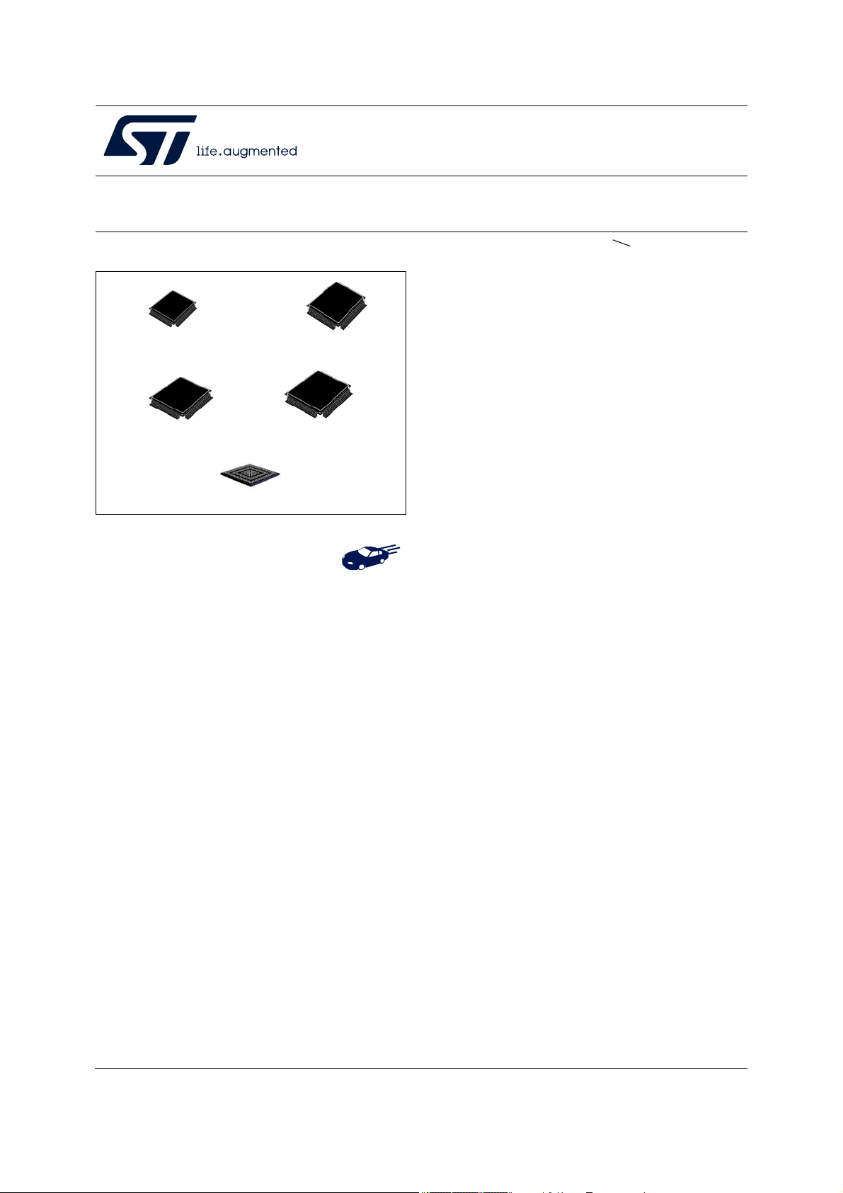
eTQFP100 (14 x 14 x 1.0 mm)
eTQFP64 (10 x 10 x 1.0 mm)
eTQFP144 (20 x 20 x 1.0 mm)
FPBGA292 (17 x 17 x 1.8 mm)
eLQFP176 (24 x 24 x 1.4 mm)
• AEC-Q100 qualified
• High performance e200z420n3 dual core
– 32-bit Power Architecture technology CPU
– Core frequency as high as 180 MHz
– Variable Length Encoding (VLE)
• 4224 KB (4096 KB code flash + 128 KB data
flash) on-chip flash memory: supports read
during program and erase operations, and
multiple blocks allowing EEPROM emulation
• 176 KB HSM dedicated flash memory (144 KB
code + 32 KB data)
• 384 KB on-chip general-purpose SRAM (in
addition to 128 KB core local data RAM: 64 KB
included in each CPU)
• Multi-channel direct memory access controller
(eDMA) with 64 channels
• 1 interrupt controller (INTC)
• Comprehensive new generation ASIL-B safety
concept
– ASIL-B of ISO 26262
– FCCU for collection and reaction to failure
SPC584Cx, SPC58ECx
SPC58 C Line - 32 bit Power Architecture automotive MCU
Dual z4 cores 180 MHz, 4 MBytes Flash, HSM, ASIL-B
Datasheet - production data
– Memory Error Management Unit (MEMU)
for collection and reporting of error events
in memories
– Cyclic redundancy check (CRC) unit
• Crossbar switch architecture for concurrent
access to peripherals, Flash, or RAM from
multiple bus masters with end-to-end ECC
• Body cross triggering unit (BCTU)
– Triggers ADC conversions from any eMIOS
channel
– Triggers ADC conversions from up to 2
dedicated PIT_RTIs
• Enhanced modular IO subsystem (eMIOS): up
to 64 timed I/O channels with 16-bit counter
resolution
• Enhanced analog-to-digital converter system
with:
– 3 independent fast 12-bit SAR analog
converters
– 1 supervisor 12-bit SAR analog converter
– 1 10-bit SAR analog converter with STDBY
mode support
• Communication interfaces
– 18 LINFlexD modules
– 8 deserial serial peripheral interface (DSPI)
modules
– 8 MCAN interfaces with advanced shared
memory scheme and ISO CAN-FD support
– Dual-channel FlexRay controller
– 1 ethernet controller 10/100 Mbps,
compliant IEEE 802.3-2008
• Low power capabilities
– Versatile low power modes
– Ultra low power standby with RTC
– Smart Wake-up Unit for contact monitoring
– Fast wakeup schemes
• Dual phase-locked loops with stable clock
notifications
domain for peripherals and FM modulation
domain for computational shell
July 2020 DS11620 Rev 7 1/153
This is information on a product in full production.
www.st.com
SPC584Cx, SPC58ECx
• Nexus development interface (NDI) per IEEE-ISTO 5001-2003 standard, with some
support for 2010 standard
• Boot assist Flash (BAF) supports factory programming using a serial bootload through the
asynchronous CAN or LIN/UART
• Junction temperature range -40 °C to 150 °C
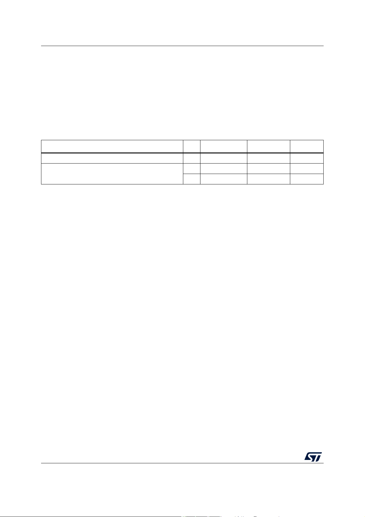
Table 1. Device summary
Part number
Package
2 MB 3 MB 4 MB
Single core Dual core Single core Dual core Single core Dual core
eTQFP64 SPC584C70E1 SPC58EC70E1 SPC584C74E1 SPC58EC74E1 SPC584C80E1 SPC58EC80E1
eTQFP100 SPC584C70E3 SPC58EC70E3 SPC584C74E3 SPC58EC74E3 SPC584C80E3 SPC58EC80E3
eTQFP144 SPC584C70E5 SPC58EC70E5 SPC584C74E5 SPC58EC74E5 SPC584C80E5 SPC58EC80E5
eLQFP176 SPC584C70E7 SPC58EC70E7 SPC584C74E7 SPC58EC74E7 SPC584C80E7 SPC58EC80E7
FPBGA292 SPC584C70C3 SPC58EC70C3 SPC584C74C3 SPC58EC74C3 SPC584C80C3 SPC58EC80C3
2/153 DS11620 Rev 7

SPC584Cx, SPC58ECx Contents
Contents
1 Introduction . . . . . . . . . . . . . . . . . . . . . . . . . . . . . . . . . . . . . . . . . . . . . . . . 6
2 Description . . . . . . . . . . . . . . . . . . . . . . . . . . . . . . . . . . . . . . . . . . . . . . . . . 7
2.1 Device feature summary . . . . . . . . . . . . . . . . . . . . . . . . . . . . . . . . . . . . . . 7
2.2 Block diagram . . . . . . . . . . . . . . . . . . . . . . . . . . . . . . . . . . . . . . . . . . . . . . . 8
2.3 Features overview . . . . . . . . . . . . . . . . . . . . . . . . . . . . . . . . . . . . . . . . . . .11
3 Package pinouts and signal descriptions . . . . . . . . . . . . . . . . . . . . . . . 13
4 Electrical characteristics . . . . . . . . . . . . . . . . . . . . . . . . . . . . . . . . . . . . 14
4.1 Introduction . . . . . . . . . . . . . . . . . . . . . . . . . . . . . . . . . . . . . . . . . . . . . . . 14
4.2 Absolute maximum ratings . . . . . . . . . . . . . . . . . . . . . . . . . . . . . . . . . . . . 15
4.3 Operating conditions . . . . . . . . . . . . . . . . . . . . . . . . . . . . . . . . . . . . . . . . 17
4.3.1 Power domains and power up/down sequencing . . . . . . . . . . . . . . . . . 19
4.4 Electrostatic discharge (ESD) . . . . . . . . . . . . . . . . . . . . . . . . . . . . . . . . . 20
4.5 Electromagnetic compatibility characteristics . . . . . . . . . . . . . . . . . . . . . . 21
4.6 Temperature profile . . . . . . . . . . . . . . . . . . . . . . . . . . . . . . . . . . . . . . . . . 22
4.7 Device consumption . . . . . . . . . . . . . . . . . . . . . . . . . . . . . . . . . . . . . . . . . 23
4.8 I/O pad specification . . . . . . . . . . . . . . . . . . . . . . . . . . . . . . . . . . . . . . . . . 26
4.8.1 I/O input DC characteristics . . . . . . . . . . . . . . . . . . . . . . . . . . . . . . . . . . 26
4.8.2 I/O output DC characteristics . . . . . . . . . . . . . . . . . . . . . . . . . . . . . . . . . 29
4.8.3 I/O pad current specifications . . . . . . . . . . . . . . . . . . . . . . . . . . . . . . . . 34
4.9 Reset pad (PORST) electrical characteristics . . . . . . . . . . . . . . . . . . . . . 37
4.10 PLLs . . . . . . . . . . . . . . . . . . . . . . . . . . . . . . . . . . . . . . . . . . . . . . . . . . . . . 40
4.10.1 PLL0 . . . . . . . . . . . . . . . . . . . . . . . . . . . . . . . . . . . . . . . . . . . . . . . . . . . 40
4.10.2 PLL1 . . . . . . . . . . . . . . . . . . . . . . . . . . . . . . . . . . . . . . . . . . . . . . . . . . . 42
4.11 Oscillators . . . . . . . . . . . . . . . . . . . . . . . . . . . . . . . . . . . . . . . . . . . . . . . . . 43
4.11.1 Crystal oscillator 40 MHz . . . . . . . . . . . . . . . . . . . . . . . . . . . . . . . . . . . . 43
4.11.2 Crystal Oscillator 32 kHz . . . . . . . . . . . . . . . . . . . . . . . . . . . . . . . . . . . . 44
4.11.3 RC oscillator 16 MHz . . . . . . . . . . . . . . . . . . . . . . . . . . . . . . . . . . . . . . . 45
4.11.4 Low power RC oscillator . . . . . . . . . . . . . . . . . . . . . . . . . . . . . . . . . . . . 46
4.12 ADC system . . . . . . . . . . . . . . . . . . . . . . . . . . . . . . . . . . . . . . . . . . . . . . . 47
4.12.1 ADC input description . . . . . . . . . . . . . . . . . . . . . . . . . . . . . . . . . . . . . . 47
DS11620 Rev 7 3/153
5

Contents SPC584Cx, SPC58ECx
4.12.2 SAR ADC 12-bit electrical specification . . . . . . . . . . . . . . . . . . . . . . . . . 48
4.12.3 SAR ADC 10-bit electrical specification . . . . . . . . . . . . . . . . . . . . . . . . . 53
4.13 Temperature Sensor . . . . . . . . . . . . . . . . . . . . . . . . . . . . . . . . . . . . . . . . . 56
4.14 LFAST pad electrical characteristics . . . . . . . . . . . . . . . . . . . . . . . . . . . . 57
4.14.1 LFAST interface timing diagrams . . . . . . . . . . . . . . . . . . . . . . . . . . . . . . 57
4.14.2 LFAST LVDS interface electrical characteristics . . . . . . . . . . . . . . . . . . 58
4.14.3 LFAST PLL electrical characteristics . . . . . . . . . . . . . . . . . . . . . . . . . . . 61
4.15 Power management . . . . . . . . . . . . . . . . . . . . . . . . . . . . . . . . . . . . . . . . . 63
4.15.1 Power management integration . . . . . . . . . . . . . . . . . . . . . . . . . . . . . . . 63
4.15.2 Voltage regulators . . . . . . . . . . . . . . . . . . . . . . . . . . . . . . . . . . . . . . . . . 69
4.15.3 Voltage monitors . . . . . . . . . . . . . . . . . . . . . . . . . . . . . . . . . . . . . . . . . . 70
4.16 Flash . . . . . . . . . . . . . . . . . . . . . . . . . . . . . . . . . . . . . . . . . . . . . . . . . . . . 73
4.17 AC Specifications . . . . . . . . . . . . . . . . . . . . . . . . . . . . . . . . . . . . . . . . . . . 77
4.17.1 Debug and calibration interface timing . . . . . . . . . . . . . . . . . . . . . . . . . 77
4.17.2 DSPI timing with CMOS pads . . . . . . . . . . . . . . . . . . . . . . . . . . . . . . . . 83
4.17.3 Ethernet timing . . . . . . . . . . . . . . . . . . . . . . . . . . . . . . . . . . . . . . . . . . . . 93
4.17.4 FlexRay timing . . . . . . . . . . . . . . . . . . . . . . . . . . . . . . . . . . . . . . . . . . . . 99
4.17.5 CAN timing . . . . . . . . . . . . . . . . . . . . . . . . . . . . . . . . . . . . . . . . . . . . . . 103
4.17.6 UART timing . . . . . . . . . . . . . . . . . . . . . . . . . . . . . . . . . . . . . . . . . . . . . 103
4.17.7 I2C timing . . . . . . . . . . . . . . . . . . . . . . . . . . . . . . . . . . . . . . . . . . . . . . . 104
5 Package information . . . . . . . . . . . . . . . . . . . . . . . . . . . . . . . . . . . . . . . 106
5.1 eTQFP64 package information . . . . . . . . . . . . . . . . . . . . . . . . . . . . . . . 106
5.1.1 Package mechanical drawings and data information . . . . . . . . . . . . . 110
5.2 eTQFP100 package information . . . . . . . . . . . . . . . . . . . . . . . . . . . . . . . 111
5.2.1 Package mechanical drawings and data information . . . . . . . . . . . . . 115
5.3 eTQFP144 package information . . . . . . . . . . . . . . . . . . . . . . . . . . . . . . .116
5.3.1 Package mechanical drawings and data information . . . . . . . . . . . . . 120
5.4 eLQFP176 package information . . . . . . . . . . . . . . . . . . . . . . . . . . . . . . . 121
5.4.1 Package mechanical drawings and data information . . . . . . . . . . . . . 125
5.5 FPBGA292 package information . . . . . . . . . . . . . . . . . . . . . . . . . . . . . . 126
5.5.1 Package mechanical drawings and data information . . . . . . . . . . . . . 128
5.6 Package thermal characteristics . . . . . . . . . . . . . . . . . . . . . . . . . . . . . . 130
5.6.1 eTQFP64 . . . . . . . . . . . . . . . . . . . . . . . . . . . . . . . . . . . . . . . . . . . . . . . 130
5.6.2 eTQFP100 . . . . . . . . . . . . . . . . . . . . . . . . . . . . . . . . . . . . . . . . . . . . . . 130
5.6.3 eTQFP144 . . . . . . . . . . . . . . . . . . . . . . . . . . . . . . . . . . . . . . . . . . . . . . 131
4/153 DS11620 Rev 7

SPC584Cx, SPC58ECx Contents
5.6.4 LQFP176 . . . . . . . . . . . . . . . . . . . . . . . . . . . . . . . . . . . . . . . . . . . . . . . 132
5.6.5 FPBGA292 . . . . . . . . . . . . . . . . . . . . . . . . . . . . . . . . . . . . . . . . . . . . . . 133
5.6.6 General notes for specifications at maximum junction temperature . . 133
6 Ordering information . . . . . . . . . . . . . . . . . . . . . . . . . . . . . . . . . . . . . . 136
7 Revision history . . . . . . . . . . . . . . . . . . . . . . . . . . . . . . . . . . . . . . . . . . 140
DS11620 Rev 7 5/153
5

Introduction SPC584Cx, SPC58ECx
1 Introduction
This document describes the features of the family and options available within the family
members, and highlights important electrical and physical characteristics of the device. To
ensure a complete understanding of the device functionality, refer also to the device
reference manual and errata sheet.
6/153 DS11620 Rev 7
SPC584Cx, SPC58ECx Description
2 Description
The SPC584Cx and SPC58ECx microcontroller is the first in a new family of devices
superseding the SPC564Cx and SPC56ECx family. SPC584Cx and SPC58ECx builds on
the legacy of the SPC564Cx and SPC56ECx family, while introducing new features coupled
with higher throughput to provide substantial reduction of cost per feature and significant
power and performance improvement (MIPS per mW). On the SPC584Cx and SPC58ECx
device, there are two processor cores e200z420 and one e200z0 core embedded in the
Hardware Security Module.
2.1 Device feature summary
Table 2 lists a summary of major features for the SPC584Cx and SPC58ECx device. The
feature column represents a combination of module names and capabilities of certain
modules. A detailed description of the functionality provided by each on-chip module is
given later in this document.
Feature Description
Table 2. Features List
SPC58 family 40 nm
Number of Cores 2
Local RAM 2x 64 KB Data
Single Precision Floating Point Yes
SIMD No
VLE Yes
Cache
MPU
Semaphores Yes
CRC Channels 2 x 4
Software Watchdog Timer (SWT) 3
Core Nexus Class 3+
Event Processor
Run control Module Yes
System SRAM 384 KB (including 256 KB of standby RAM)
8 KB Instruction
4 KB Data
Core MPU: 24 per CPU
System MPU: 24 per XBAR
4 x SCU
4 x PMC
Flash 4096 KB code / 128 KB data
Flash fetch accelerator 2 x 4 x 256-bit
DMA channels 64
DS11620 Rev 7 7/153
12
Description SPC584Cx, SPC58ECx
Table 2. Features List (continued)
Feature Description
DMA Nexus Class 3
LINFlexD 18
MCAN (ISO CAN-FD compliant) 8
DSPI 8
I2C 1
FlexRay 1 x Dual channel
Ethernet 1 MAC with Time Stamping, AVB and VLAN support
SIPI / LFAST Debugger High Speed
8 PIT channels
System Timers
eMIOS 2 x 32 channels
BCTU 64 channels
Interrupt controller 1 x 568 sources
ADC (SAR) 5
4 AUTOSAR® (STM)
RTC/API
Temp. sensor Yes
Self Test Controller Yes
PLL Dual PLL with FM
Integrated linear voltage regulator Yes
External Power Supplies 5 V, 3.3 V
Low Power Modes
2.2 Block diagram
The figures below show the top-level block diagrams.
HALT Mode
STOP Mode
Smart Standby with output controller, analog and digital inputs
Standby Mode
8/153 DS11620 Rev 7
SPC584Cx, SPC58ECx Description
Delayed Lock-step with Redundancy Checkers
Delayed Lock-step with Redundancy Checkers
Instruction
32 ADD
64 DATA
Load / Store
32 ADD
64 DATA
M4
M5
FLASH
4 MB
EEPROM
4x32 KB
Non Volatile Memory
Multiple RWW partitions
256 Page Line
EFPU2VLE
Core Memory Protection Unit
(CMPU)
e200 z420n3
– 180 MHz
dual issue
Main Core_0
Nexus3p
BIU with E2E ECC
Decorated Storage Access
SWT_0 IAC
S5
System Memory Protection Unit
Cross Bar Switch (XBAR) AMBA 2.0 v6 AHB – 64 bits
Unified
Backdoor
Interface
With
E2E ECC
S7
Periph.
Bridge 2
E2E ECC
Peripheral
Cluster 2
32 ADD
64 DATA
32 ADD
32 DATA
Periph.
Bridge 1
E2E ECC
Peripheral
Cluster 1
32 ADD
64 DATA
32 ADD
32 DATA
PRAMC_3
with E2E
ECC
32 ADD
64 DATA
SRAM
Array 3
128 KB
32 ADD
64 DATA
PRAMC_2
with E2E
ECC
32 ADD
64 DATA
SRAM
Array 2
256 KB
32 ADD
64 DATA
PFLASHC_1
Set-Associative Prefetch
Buffers
with E2E ECC
32 ADD
64 DATA
S4
S2 S0
S1
S6
M0 M1
S3
SPUDCIJTAGCJTAGM NPC
32 ADD
64 DATA
FlexRay_0
M3
Nexus Data
Trace
ETHERNET_0
Nexus Data
Trace
HSM
32 ADD
64 DATA
32 ADD
64 DATA
M2
Concentrator_1
E2E ECC
PAMU
SWT_2 IAC
Delayed Lock-step with Redundancy Checkers
Instruction
32 ADD
64 DATA
Load / Store
32 ADD
64 DATA
e200 z420n3 – 180 MHz
dual issue
Main Core_2
Nexus3p
VLE EFPU2
Unified
Backdoor
Interface
With
E2E ECC
Core Memory Protection Unit
(CMPU)
BIU with E2E ECC
Decorated Storage Access
INTC
I-Cache
Control
8 KB
2 way
D-MEM
Control
64 KB
D-MEM
D-Cache
Control
4 KB
2 way
I-Cache
Control
8 KB
2 way
D-MEM
Control
64 KB
D-MEM
D-Cache
Control
4 KB
2 way
SIPI_1
Nexus Data
Trace
32 ADD
64 DATA
M6
32 ADD
64 DATA
DMA CHMUX_1
64 Ch
eDMA_1
DMA CHMUX_2
DMA CHMUX_0
DMA CHMUX_3
Figure 1. Block diagram
DS11620 Rev 7 9/153
12
Description SPC584Cx, SPC58ECx
Note:
In this diagram, ON-platform modules are shown in orange color and OFF-platform modules
are shown in blue color.
3%5,'*(B±3HULSKHUDO&OXVWHU
3%5,'*(B±3HULSKHUDO&OXVWHU
%&78B
H0,26B
3%5,'*(B
;%$5B
;%,&B&RQFHQWUDWRUB
6038B
;%,&B
3&0B
3)/$6+B
6(0
,17&B
6:7B
670B
H'0$B
35$0B
7'0B
67'%<B&78B
H0,26B
(7+(51(7B
6$5B$'&BELWB
6$5B$'&BELWB67'%<
6$5B$'&BELWB%
)/(;5$<B
,&B
'63,B
/,1)OH['B
&$1B68%BB0(66$*(B5$0
&$1B68%BB0B&$1B
&&&8
+60
'76
-'&
67&8
-7$*0
0(08
,0$
&5&B
'0$08;B
3,7B
57&$3,
:.38
0&B3&8
30&B',*
0&B5*0
5&26&B',*
5&.B',*
26&B',*
26&.B',*
3//B',*
&08BB3//B;26&B,5&26&
0&B&*0
0&B0(
6,8/
)/$6+B
)/$6+B$/7B
3$66
66&0
3%5,'*(B
6$5B$'&BELWB
'63,B
/,1)OH['B
&$1B68%BB0(66$*(B5$0
&$1B68%BB0B&$1B
)&&8
&5&B
'0$08;B
3,7B
&08BB&25(B;%$5
&08BB+3%0
&08BB3%5,'*(
&08BB6$5$'&
&08BB)%5,'*(
&08BB(0,26
&08BB3)%5,'*(
6,3,B
/)$67B
Figure 2. Periphery allocation
10/153 DS11620 Rev 7

SPC584Cx, SPC58ECx Description
2.3 Features overview
On-chip modules within SPC584Cx and SPC58ECx include the following features:
• Two main CPUs, dual issue, 32-bit CPU core complexes (e200z4).
– Power Architecture embedded specification compliance
– Instruction set enhancement allowing variable length encoding (VLE), encoding a
mix of 16-bit and 32-bit instructions, for code size footprint reduction
– Single-precision floating point operations
– 64 KB local data RAM for Core_0 and Core_2
– 8 KB I-Cache and 4 KB D-Cache for Core_0 and Core_2
• 4224 KB (4096 KB code flash + 128 KB data flash) on-chip flash memory
– Supports read during program and erase operations, and multiple blocks allowing
EEPROM emulation
• 176 KB HSM dedicated flash memory (144 KB code + 32 KB data)
• 384 KB on-chip general-purpose SRAM (+ 128 KB local data RAM: 64 KB included in
each CPU)
• Multi channel direct memory access controllers
– 64 eDMA channels
• One interrupt controller (INTC)
• Dual phase-locked loops with stable clock domain for peripherals and FM modulation
domain for computational shell
• Crossbar switch architecture for concurrent access to peripherals, Flash, or RAM from
multiple bus masters with end-to-end ECC
• Hardware security module (HSM) with HW cryptographic co-processor
• System integration unit lite (SIUL)
• Boot assist Flash (BAF) supports factory programming using a serial bootload through the
asynchronous CAN or LIN/UART.
• Hardware support for safety ASIL-B level related applications
• Enhanced modular IO subsystem (eMIOS): up to 64 (2 x 32) timed I/O channels with
16-bit counter resolution
– Buffered updates
– Support for shifted PWM outputs to minimize occurrence of concurrent edges
– Supports configurable trigger outputs for ADC conversion for synchronization to
channel output waveforms
– Shared or independent time bases
– DMA transfer support available
• Body cross triggering unit (BCTU)
– Triggers ADC conversions from any eMIOS channel
– Triggers ADC conversions from up to 2 dedicated PIT_RTIs
– One event configuration register dedicated to each timer event allows to define the
corresponding ADC channel
– Synchronization with ADC to avoid collision
DS11620 Rev 7 11/153
12

Description SPC584Cx, SPC58ECx
• Enhanced analog-to-digital converter system with:
– Three independent fast 12-bit SAR analog converters
– One supervisor 12-bit SAR analog converter
– One 10-bit SAR analog converter with STDBY mode support
• Eight deserial serial peripheral interface (DSPI) modules
• Eighteen LIN and UART communication interface (LINFlexD) modules
– LINFlexD_0 is a Master/Slave
– All others are Masters
• Eight modular controller area network (MCAN) modules, all supporting flexible data rate
(ISO CAN-FD compliant)
• Dual-channel FlexRay controller
• One ethernet controller 10/100 Mbps, compliant IEEE 802.3-2008
– IEEE 1588-2008 Time stamping (internal 64-bit time stamp)
– IEEE 802.1AS and IEEE 802.1Qav (AVB-Feature)
– IEEE 802.1Q VLAN tag detection
– IPv4 and IPv6 checksum modules
• Nexus development interface (NDI) per IEEE-ISTO 5001-2003 standard, with some
support for 2010 standard.
• Device and board test support per Joint Test Action Group (JTAG) (IEEE 1149.1 and
IEEE 1149.7), 2-pin JTAG interface.
• Standby power domain with smart wake-up sequence
12/153 DS11620 Rev 7

SPC584Cx, SPC58ECx Package pinouts and signal descriptions
3 Package pinouts and signal descriptions
Refer to the SPC584Cx and SPC58ECx IO_ Definition document.
It includes the following sections:
1. Package pinouts
2. Pin descriptions
a) Power supply and reference voltage pins
b) System pins
c) LVDS pins
d) Generic pins
DS11620 Rev 7 13/153
13
Electrical characteristics SPC584Cx, SPC58ECx
4 Electrical characteristics
4.1 Introduction
The present document contains the target Electrical Specification for the 40 nm family 32-bit
MCU SPC584Cx and SPC58ECx products.
In the tables where the device logic provides signals with their respective timing
characteristics, the symbol “CC” (Controller Characteristics) is included in the “Symbol”
column.
In the tables where the external system must provide signals with their respective timing
characteristics to the device, the symbol “SR” (System Requirement) is included in the
“Symbol” column.
The electrical parameters shown in this document are guaranteed by various methods. To
give the customer a better understanding, the classifications listed in Table 3 are used and
the parameters are tagged accordingly in the tables where appropriate.
Classification tag Tag description
Table 3. Parameter classifications
P Those parameters are guaranteed during production testing on each individual device.
C Those parameters are achieved by the design characterization by measuring a statistically
relevant sample size across process variations.
T Those parameters are achieved by design validation on a small sample size from typical
devices.
D Those parameters are derived mainly from simulations.
14/153 DS11620 Rev 7
SPC584Cx, SPC58ECx Electrical characteristics
4.2 Absolute maximum ratings
Table 4 describes the maximum ratings for the device. Absolute maximum ratings are stress
ratings only, and functional operation at the maxima is not guaranteed. Exposure to
absolute maximum rating conditions for extended periods may affect device reliability.
Stress beyond the listed maxima, even momentarily, may affect device reliability or cause
permanent damage to the device.
Symbol C Parameter Conditions
V
DD_LV
V
DD_HV_IO_MAIN
V
DD_HV_IO_FLEX
V
DD_HV_OSC
V
DD_HV_FLA
V
SS_HV_ADV
V
DD_HV_ADV
V
SS_HV_ADR_S
SR D
SR D
SR D
SR D
SR D
Table 4. Absolute maximum ratings
Core voltage
operating life
(1)
range
I/O supply
voltage
(2)
ADC ground
voltage
ADC Supply
voltage
(2)
SAR ADC
ground
reference
— –0.3 — 1.4 V
— –0.3 — 6.0 V
Reference to
digital ground
Reference to
V
SS_HV_ADV
— –0.3 — 0.3 V
Value
Unit
Min Typ Max
–0.3 — 0.3 V
–0.3 — 6.0 V
V
DD_HV_ADR_S
V
SS-VSS_HV_ADR_S
V
SS-VSS_HV_ADV
V
IN
T
TRIN
I
INJ
SR D
SR D
SR D
SR D
SR D
SR T
SAR ADC
voltage
reference
V
SS_HV_ADR_S
(2)
differential
voltage
V
SS_HV_ADV
differential
voltage
I/O input voltage
(2)(3) (4)
range
Digital Input pad
transition time
(5)
Maximum DC
injection current
for each
analog/digital
PAD
(6)
Reference to
V
SS_HV_ADR_S
–0.3 — 6.0 V
— –0.3 — 0.3 V
— –0.3 — 0.3 V
— –0.3 — 6.0
Relative to V
Relative to
V
DD_HV_IO
V
DD_HV_ADV
and
ss
–0.3 — —
V
——0.3
———1ms
—–5—5mA
DS11620 Rev 7 15/153
16
Electrical characteristics SPC584Cx, SPC58ECx
Table 4. Absolute maximum ratings (continued)
Value
Symbol C Parameter Conditions
Maximum non-
operating
T
STG
SR T
Storage
— –55 — 125 °C
temperature
range
Maximum non-
operating
T
PAS
SR C
temperature
—–55—150
during passive
lifetime
Min Typ Max
(7)
Unit
°C
T
STORAGE
SR —
Maximum
storage time,
assembled part
programmed in
ECU
No supply; storage
temperature in
range –40 °C to
60 °C
— — 20 years
Maximum solder
T
SDR
SR T
temperature Pbfree packaged
(8)
———260°C
Moisture
MSL SR T
sensitivity
(9)
level
———3—
Typical range for
X-rays source
during
inspection:80 ÷
130 KV; 20 ÷
—— 1grey
dose SR T
T
XRAY
Maximum
cumulated
XRAY dose
50 μA
1. V
2. V
3. The maximum input voltage on an I/O pin tracks with the associated I/O supply maximum. For the injection current
4. Relative value can be exceeded if design measures are taken to ensure injection current limitation (parameter IINJ).
5. This limitation applies to pads with digital input buffer enabled. If the digital input buffer is disabled, there are no maximum
6. The limits for the sum of all normal and injected currents on all pads within the same supply segment can be found in
7. 175°C are allowed for limited time. Mission profile with passive lifetime temperature >150°C have to be evaluated by ST to
8. Solder profile per IPC/JEDEC J-STD-020D.
9. Moisture sensitivity per JDEC test method A112.
: allowed 1.335 V - 1.400 V for 60 seconds cumulative time at the given temperature profile. Remaining time allowed
DD_LV
1.260 V - 1.335 V for 10 hours cumulative time at the given temperature profile. Remaining time as defined in Section 4.3:
Operating conditions.
: allowed 5.5 V – 6.0 V for 60 seconds cumulative time at the given temperature profile, for 10 hours cumulative
DD_HV
time with the device in reset at the given temperature profile. Remaining time as defined in Section 4.3: Operating
conditions.
condition on a pin, the voltage will be equal to the supply plus the voltage drop across the internal ESD diode from I/O pin
to supply. The diode voltage varies greatly across process and temperature, but a value of 0.3 V can be used for nominal
calculations.
limits to the transition time.
Section 4.8.3: I/O pad current specifications.
confirm that are granted by product qualification.
16/153 DS11620 Rev 7
SPC584Cx, SPC58ECx Electrical characteristics
4.3 Operating conditions
Table 5 describes the operating conditions for the device, and for which all the specifications
in the data sheet are valid, except where explicitly noted. The device operating conditions
must not be exceeded or the functionality of the device is not guaranteed.
Symbol C Parameter Conditions
Table 5. Operating conditions
(1)
Value
Min Typ Max
Unit
(2)
F
SYS
T
A_125 Grade
T
J_125 Grade
T
A_105 Grade
T
J_105 Grade
V
DD_LV
V
DD_HV_IO_MAIN
V
DD_HV_IO_FLEX
V
DD_HV_FLA
V
DD_HV_OSC
V
DD_HV_ADV
(4)
(4)
(4)
(4)
SR P
SR D
SR P
SR D
SR D
SR P
SR P
SR P
Operating
system clock
frequency
(3)
Operating
Ambient
temperature
Junction
temperature
under bias
Ambient
temperature
under bias
Operating
Junction
temperature
Core supply
voltage
(5)
IO supply
voltage
ADC supply
voltage
———180MHz
— –40 — 125 °C
TA= 125 °C –40 — 150 °C
— –40 — 105 °C
TA= 105 °C –40 — 130 °C
— 1.14 1.20 1.26
(6) (7)
V
— 3.0 — 5.5 V
— 3.0 — 5.5 V
V
SS_HV_ADV
V
SS
V
DD_HV_ADR_S
V
DD_HV_ADR_S
V
DD_HV_ADV
V
SS_HV_ADR_S
SR D
ADC ground
differential
— –25 — 25 mV
voltage
SAR ADC
SR P
reference
— 3.0 — 5.5 V
voltage
SAR ADC
SR D
reference
differential
———25mV
voltage
SAR ADC
SR P
ground
reference
—V
SS_HV_ADV
V
voltage
DS11620 Rev 7 17/153
19
Electrical characteristics SPC584Cx, SPC58ECx
Table 5. Operating conditions (continued)
(1)
Value
Symbol C Parameter Conditions
Min Typ Max
Unit
V
SS_HV_ADR_S
V
SS_HV_ADV
SR D
V
SS_HV_ADR_S
differential
voltage
— –25 — 25 mV
Slew rate on
V
RAMP_HV
SR D
HV power
———100V/ms
supply
V
IN
SR P
I/O input
voltage range
—0—5.5V
Injection
current (per
I
INJ1
SR T
pin) without
performance
degradation
(9) (10)
Digital pins and
analog pins
(8)
–3.0 — 3.0 mA
Dynamic
Injection
current (per
I
INJ2
SR D
pin) with
performance
degradation
(11)
1. The ranges in this table are design targets and actual data may vary in the given range.
2. The maximum number of PRAM wait states has to be configured accordingly to the system clock frequency. Refer to
Table 6.
3. Maximum operating frequency is applicable to the cores and platform of the device. See the Clock Chapter in the
Microcontroller Reference Manual for more information on the clock limitations for the various IP blocks on the device.
4. In order to evaluate the actual difference between ambient and junction temperatures in the application, refer to
Section 5.6: Package thermal characteristics.
5. Core voltage as measured on device pin to guarantee published silicon performance.
6. Core voltage can exceed 1.26 V with the limitations provided in Section 4.2: Absolute maximum ratings, provided that
HVD134_C monitor reset is disabled.
7. 1.260 V - 1.290 V range allowed periodically for supply with sinusoidal shape and average supply value below or equal to
1.236 V at the given temperature profile.
8. Full device lifetime. I/O and analog input specifications are only valid if the injection current on adjacent pins is within these
limits. See Section 4.2: Absolute maximum ratings for maximum input current for reliability requirements.
9. The I/O pins on the device are clamped to the I/O supply rails for ESD protection. When the voltage of the input pins is
above the supply rail, current will be injected through the clamp diode to the supply rails. For external RC network
calculation, assume typical 0.3 V drop across the active diode. The diode voltage drop varies with temperature.
10. The limits for the sum of all normal and injected currents on all pads within the same supply segment can be found in
Section 4.8.3: I/O pad current specifications.
11. Positive and negative Dynamic current injection pulses are allowed up to this limit. I/O and ADC specifications are not
granted. See the dedicated chapters for the different specification limits. See the Absolute Maximum Ratings table for
maximum input current for reliability requirements. Refer to the following pulses definitions: Pulse1 (ISO 7637-2:2011),
Pulse 2a(ISO 7637-2:2011 5.6.2), Pulse 3a (ISO 7637-2:2011 5.6.3), Pulse 3b (ISO 7637-2:2011 5.6.3).
Digital pins and
analog pins
(10)
–10 — 10 mA
18/153 DS11620 Rev 7
SPC584Cx, SPC58ECx Electrical characteristics
Table 6. PRAM wait states configuration
PRAMC WS Clock Frequency (MHz)
1<
0<
4.3.1 Power domains and power up/down sequencing
The following table shows the constraints and relationships for the different power domains.
Supply1 (on rows) can exceed Supply2 (on columns), only if the cell at the given row and
column is reporting ‘ok’. This limitation is valid during power-up and power-down phases, as
well as during normal device operation.
Table 7. Device supply relation during power-up/power-down sequence
Supply2
V
DD_HV_IO_MAIN
V
DD_HV_FLA
V
DD_HV_OSC
V
V
Supply1
DD_HV_IO_FLEX
DD_HV_IO_MAIN
V
DD_HV_FLA
V
DD_HV_OSC
V
DD_HV_ADV
V
DD_HV_ADR
V
DD_LV
V
DD_HV_IO_FLEX
ok not allowed ok ok
ok ok ok ok
ok ok not allowed ok
ok ok not allowed not allowed
180
120
V
DD_HV_ADV
V
DD_HV_ADR
During power-up, all functional terminals are maintained in a known state as described in
the device pinout Microsoft Excel file attached to the IO_Definition document.
DS11620 Rev 7 19/153
19
Electrical characteristics SPC584Cx, SPC58ECx
4.4 Electrostatic discharge (ESD)
The following table describes the ESD ratings of the device:
• All ESD testing are in conformity with CDF-AEC-Q100 Stress Test Qualification for
Automotive Grade Integrated Circuits,
• Device failure is defined as: “If after exposure to ESD pulses, the device does not meet
the device specification requirements, which include the complete DC parametric and
functional testing at room temperature and hot temperature, maximum DC parametric
variation within 10% of maximum specification”.
Parameter C Conditions Value Unit
ESD for Human Body Model (HBM)
ESD for field induced Charged Device Model (CDM)
1. This parameter tested in conformity with ANSI/ESD STM5.1-2007 Electrostatic Discharge Sensitivity Testing.
2. This parameter tested in conformity with ANSI/ESD STM5.3-1990 Charged Device Model - Component Level.
(1)
Table 8. ESD ratings
T All pins 2000 V
(2)
T All pins 500 V
T Corner Pins 750 V
20/153 DS11620 Rev 7

SPC584Cx, SPC58ECx Electrical characteristics
4.5 Electromagnetic compatibility characteristics
EMC measurements at IC-level IEC standards are available from STMicroelectronics on
request.
DS11620 Rev 7 21/153
21

Electrical characteristics SPC584Cx, SPC58ECx
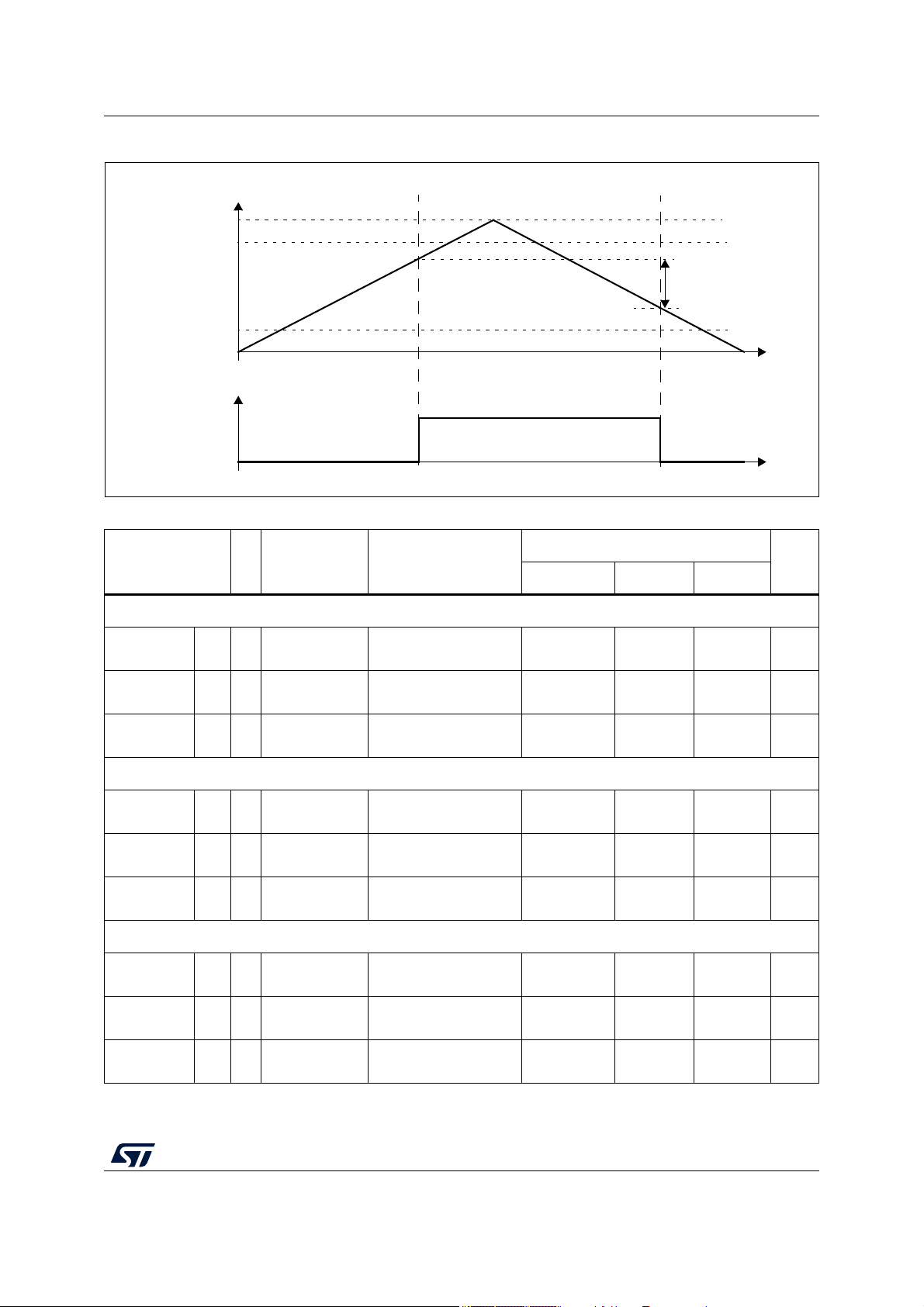
4.6 Temperature profile
The device is qualified in accordance to AEC-Q100 Grade1 requirements, such as HTOL
1,000 h and HTDR 1,000 hrs, T
Mission profile exceeding AEC-Q100 Grade 1, and with junction Temperature equal to or
lower than 150 °C have to be evaluated by ST to confirm that are covered by product
qualification. Contact your STMicroelectronics Sales representative for validation.
=150°C.
J
22/153 DS11620 Rev 7
SPC584Cx, SPC58ECx Electrical characteristics
4.7 Device consumption
Symbol C Parameter Conditions
I
I
DD_MAIN_CORE_AC
(2),(3)
DD_LKG
(3)
I
DD_LV
I
DD_HV
I
DD_LV_GW
I
DD_HV_GW
I
DD_LV_BCM
I
DD_HV_BCM
I
DD_HSM_AC
Table 9. Device consumption
C
DT
DT
CC
Leakage current on the
V
supply
DT
DD_LV
DT
PT
Dynamic current on
CC P
CC P
the V
very high consumption
Total current on the
V
DD_HV
DD_LV
profile
supply
supply,
(4)
(4)
Dynamic current on
CC T
the V
DD_LV
supply,
gateway profile
(5)
Dynamic current on
CC T
the V
DD_HV
supply,
gateway profile
(5)
Dynamic current on
CC T
the V
DD_LV
body profile
supply,
(6)
Dynamic current on
CC T
CC T
CC T
the V
body profile
Main Core dynamic
HSM platform dynamic
operating current
DD_HV
current
supply,
(6)
(7)
(8)
=40°C — — 14
T
J
=25°C — — 10
J
=55°C — — 20
J
=95°C — — 50
J
= 120 °C — — 90
J
= 150 °C — — 180
J
— — — 210 mA
f
MAX
— — — 170 mA
———37mA
— — — 150 mA
———44mA
f
MAX
f
/2 — — 20 mA
MAX
(1)
Value
Unit
Min Typ Max
mA
——64mA
——50mA
I
DDHALT
I
DDSTOP
(9)
(10)
CC T
CC T
Dynamic current on
DD_LV
supply
the V
+Total current on the
DD_HV
supply
V
Dynamic current on
DD_LV
supply
the V
+Total current on the
DD_HV
supply
V
DS11620 Rev 7 23/153
— — 71 100 mA
— — 15 30 mA
25
Electrical characteristics SPC584Cx, SPC58ECx
Table 9. Device consumption (continued)
(1)
Value
Symbol C Parameter Conditions
Min Typ Max
Unit
I
DDSTBY8
I
DDSTBY32
I
DDSTBY256
D
Total standby mode
CC
current on V
DT
V
DT
DD_HV
RAM
supply, 8 KB
DD_LV
(11)
and
PT
D
Total standby mode
CC
V
supply, 32 KB
DD_HV
DT
RAM
current on V
DT
DD_LV
(11)
and
PT
D
Total standby mode
CC
DT
V
DD_HV
256 KB RAM
current on V
DT
DD_LV
supply,
(11)
and
PT
TJ= 25 °C — 85 160
= 40 °C — — 250
J
= 55 °C — — 370
J
= 120 °C — 1.2 2.2
J
= 150 °C — 2.9 5.0
J
TJ= 25 °C — 100 180
= 40 °C — — 270
J
= 55 °C — — 410
J
= 120 °C — — 2.4
J
= 150 °C — — 5.5
J
TJ= 25 °C — 150 250
= 40 °C — — 390
J
= 55 °C — — 590
J
= 120 °C — 2.0 3.5 mA
J
= 150 °C — 5.1 8
J
µACT
mA
µACT
mA
µACT
SSWU running over all
STANDBY period with
I
DDSSWU1
CC D
OPC/TU commands
execution and keeping
ADC off
(12)
TJ=40°C — 1.0 3.5 mA
SSWU running over all
STANDBY period with
I
DDSSWU2
1. The ranges in this table are design targets and actual data may vary in the given range.
2. The leakage considered is the sum of core logic and RAM memories. The contribution of analog modules is not considered,
and they are computed in the dynamic I
3. I
4. Use case: 2 x e200Z4 @180 MHz, HSM @90 MHz, all IPs clock enabled, Flash access with prefetch disabled, Flash
5. Gateway use case: Two cores running at 160 MHz, DMA, PLL, FLASH read only 25%, 8xCAN, 1xEthernet, HSM,
6. BCM use case: One Core running at 160 MHz, no lockstep no, DMA, PLL, FLASH read only 25%, 2xCAN, HSM,
(leakage current) and I
DD_LKG
consumption contributors. The tests used in validation, characterization and production are verifying that the total
consumption (leakage+dynamic) is lower or equal to the sum of the maximum values provided (I
parameters, measured separately, may exceed the maximum reported for each, depending on the operative conditions and
the software profile used.
consumption includes parallel read and program/erase, all SARADC in continuous conversion, DMA continuously triggered
by ADC conversion, 4 DSPI / 8 CAN / 2 LINFlex and 2 DSPI transmitting, 2 x EMIOS running (8 channels in OPWMT
mode), FIRC, SIRC, FXOSC, PLL0-1 running. The switching activity estimated for dynamic consumption does not include
I/O toggling, which is highly dependent on the application. Details of the software configuration are available separately.
The total device consumption is I
2xSARADC.
4xSARADC.
CC D
(dynamic current) are reported as separate parameters, to give an indication of the
DD_LV
DD_LV
OPC/TU/ADC
commands execution
and keeping ADC
DD_LV
+ I
DD_HV
and I
+ I
(13)
on
DD_HV
DD_LKG
parameters.
TJ=40°C — 3.5 5.0 mA
for the selected temperature.
DD_LKG+IDD_LV
). The two
24/153 DS11620 Rev 7

SPC584Cx, SPC58ECx Electrical characteristics
7. Dynamic consumption of one core, including the dedicated I/D-caches and I/D-MEMS contribution.
8. Dynamic consumption of the HSM module, including the dedicated memories, during the execution of Electronic Code
Book crypto algorithm on 1 block of 16 byte of shared RAM.
9. Flash in Low Power. Sysclk at 160 MHz, PLL0_PHI at 160 MHz, XTAL at 40 MHz, FIRC 16 MHz ON, RCOSC1M off.
FlexCAN: instances: 0, 1, 2, 3, 4, 5, 6, 7 ON (configured but no reception or transmission), Ethernet ON (configured but no
reception or transmission), ADC ON (continuously converting). All others IPs clock-gated.
10. Sysclk = RC16 MHz, RC16 MHz ON, RC1 MHz ON, PLL OFF. All possible peripherals off and clock gated. Flash in power
down mode.
11. STANDBY mode: device configured for minimum consumption, RC16 MHz off, RC1 MHz on, OSC32K off, SSWU off.
12. SSWU1 mode adder: FIRC = ON, SSWU clocked at 8 MHz and running over all STANDBY period, ADC off. The total
standby consumption can be obtained by adding this parameter to the IDDSTBY parameter for the selected memory size
and temperature.
13. SSWU2 mode adder: FIRC = ON, SSWU clocked at 8 MHz and running over all STANDBY period, ADC on in continuous
conversion. The total standby consumption can be obtained by adding this parameter to the I
selected memory size and temperature.
parameter for the
DDSTBY
DS11620 Rev 7 25/153
25
Electrical characteristics SPC584Cx, SPC58ECx
4.8 I/O pad specification
The following table describes the different pad type configurations.
Pad type Description
Weak configuration Provides a good compromise between transition time and low electromagnetic emission.
Medium configuration
Strong configuration Provides fast transition speed; used for fast interface.
Very strong
configuration
Table 10. I/O pad specification descriptions
Provides transition fast enough for the serial communication channels with controlled
current to reduce electromagnetic emission.
Provides maximum speed and controlled symmetric behavior for rise and fall transition.
Used for fast interface including Ethernet and FlexRay interfaces requiring fine control of
rising/falling edge jitter.
Differential
configuration
Input only pads These low input leakage pads are associated with the ADC channels.
Standby pads
A few pads provide differential capability providing very fast interface together with good
EMC performances.
These pads (LP pads) are active during STANDBY. They are configured in CMOS level
logic and this configuration cannot be changed. Moreover, when the device enters the
STANDBY mode, the pad-keeper feature is activated for LP pads. It means that:
– if the pad voltage level is above the pad keeper high threshold, a weak pull-up resistor
is automatically enabled
– if the pad voltage level is below the pad keeper low threshold, a weak pull-down resistor
is automatically enabled.
For the pad-keeper high/low thresholds please consider (VDD_HV_IO_MAIN / 2) +/-20%.
Note: Each I/O pin on the device supports specific drive configurations. See the signal description
table in the device reference manual for the available drive configurations for each I/O pin.
PMC_DIG_VSIO register has to be configured to select the voltage level (3.3 V or 5.0 V) for
each IO segment.
Logic level is configurable in running mode while it is CMOS not-configurable in STANDBY
for LP (low power) pads, so if a LP pad is used to wakeup from STANDBY, it should be
configured as CMOS also in running mode in order to prevent device wrong behavior in
STANDBY.
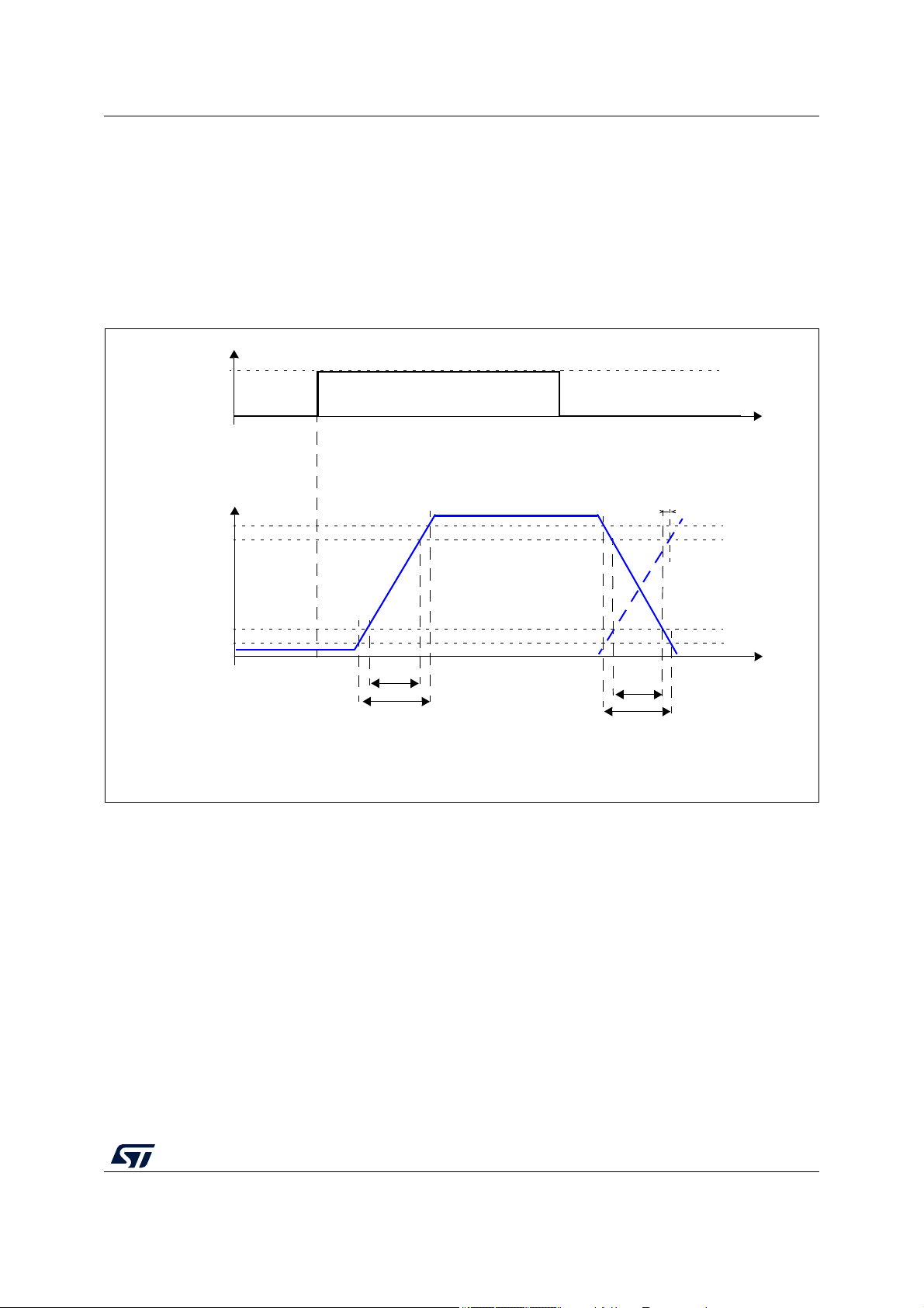
4.8.1 I/O input DC characteristics
The following table provides input DC electrical characteristics, as described in Figure 3.
26/153 DS11620 Rev 7
SPC584Cx, SPC58ECx Electrical characteristics
V
IL
V
IN
V
IH
V
INTERNAL
V
DD
V
HYS
(SIUL register)
Figure 3. I/O input electrical characteristics
Table 11. I/O input electrical characteristics
Symbol C Parameter Conditions
V
V
V
hysttl
V
ihcmos
V
ilcmos
V
hyscmos
ihttl
ilttl
SR P
SR P
CC C
SR P
SR P
CC C
Input high level
TTL
Input low level
TTL
Input hysteresis
TTL
Input high level
CMOS
Input low level
CMOS
Input hysteresis
CMOS
Value
Unit
Min Typ Max
TTL
V
—2—
DD_HV_IO
+ 0.3
V
— –0.3 — 0.8 V
—0.3——V
CMOS
DD
V
V
V
—0.65 * V
DD
—
DD_HV_IO
+ 0.3
— –0.3 — 0.35 * V
—0.10 * VDD——V
COMMON
I
LKG
I
LKG
I
LKG
CC P
CC P
CC P
Pad input
leakage
Pad input
leakage
Pad input
leakage
INPUT-ONLY pads
=150°C
T
J
STRONG pads
=150°C
T
J
VERY STRONG pads,
T
=150°C
J
——200nA
— — 1,000 nA
— — 1,000 nA
DS11620 Rev 7 27/153
36
Electrical characteristics SPC584Cx, SPC58ECx
Table 11. I/O input electrical characteristics (continued)
Value
Symbol C Parameter Conditions
Min Typ Max
Unit
C
P1
V
drift
W
FI
CC D
CC D
SR C
Pad
capacitance
Input Vil/Vih
temperature
drift
Wakeup input
filtered pulse
———10pF
In a 1 ms period, with a
temperature variation
<30 °C
(1)
———20ns
——100mV
Wakeup input
W
NFI
1. In the range from WFI (max) to W
voltage. Refer to the device pinout IO definition excel file for the list of pins supporting the wakeup filter feature.
SR C
not filtered
(1)
pulse
(min), pulses can be filtered or not filtered, according to operating temperature and
NFI
— 400 — — ns
Table 12. I/O pull-up/pull-down electrical characteristics
Value
Symbol C Parameter Conditions
Min Typ Max
(1)
= 0.69 *
(2)
= 5.0 V ±
10%
——130
15 — —
33 — 93 KΩ
I
WPU
R
WPU
CC
CC D
T
Weak pull-up
current
P
absolute value
Weak Pull-up
resistance
V
IN
V
IN
V
DD_HV_IO
V
DD_HV_IO
= 1.1 V
Unit
μA
R
I
WPD
WPU
CC D
CC
Weak Pull-up
resistance
T
Weak pull-
down current
absolute value
P
Weak Pull-
R
WPD
CC D
down
resistance
Weak Pull-
R
WPD
CC D
down
resistance
1. Maximum current when forcing a change in the pin level opposite to the pull configuration.
2. Minimum current when keeping the same pin level state than the pull configuration.
V
DD_HV_IO
VIN = 0.69 *
V
DD_HV_IO
VIN = 0.9 V
V
DD_HV_IO
V
DD_HV_IO
= 3.3 V ±
10%
= 5.0 V ±
10%
= 3.3 V ±
10%
(1)
19 — 62 KΩ
——130μA
(2)
15 — —
29 — 60 KΩ
19 — 60 KΩ
Note: When the device enters into standby mode, the LP pads have the input buffer switched-on.
As a consequence, if the pad input voltage VIN is V
SS<VIN<VDD_HV
, an additional
consumption can be measured in the VDD_HV domain. The highest consumption can be
seen around mid-range (VIN ~=VDD_HV/2), 2-3mA depending on process, voltage and
temperature.
28/153 DS11620 Rev 7
SPC584Cx, SPC58ECx Electrical characteristics
10%
V
out
V
INTERNAL
V
HYS
(SIUL register)
20%
80%
90%
t
R10-90
t
R20-80
t
F10-90
t
F20-80
tTR(max) = MAX(t
R10-90
; t
F10-90
)
t
TR
(min) = MIN(t
R10-90
; t
F10-90
)
t
TR20-80
(max) = MAX(t
R20-80
; t
F20-80
)
t
TR20-80
(min) = MIN(t
R20-80
; t
F20-80
)
t
SKEW20-80
= |t
R20-80-tF20-80
|
t
SKEW20-80
t
SKEW10-90
= |t
R10-90-tF10-90
|
This situation may occur if the PAD is used as a ADC input channel, and VSS<VIN<V
The applications should ensure that LP pads are always set to VDD_HV or VSS, to avoid
the extra consumption. Please refer to the device pinout IO definition excel file to identify the
low-power pads which also have an ADC function.
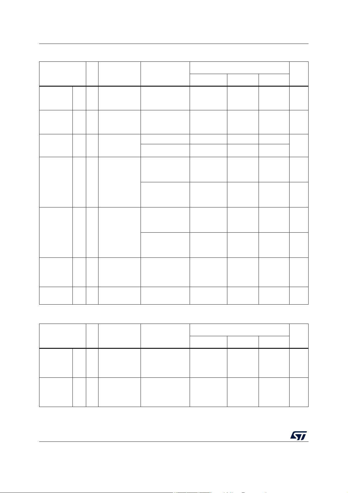
4.8.2 I/O output DC characteristics
Figure 4 provides description of output DC electrical characteristics.
Figure 4. I/O output DC electrical characteristics definition
DD_HV
.
Note: 10%/90% is the default condition for any parameter if not explicitly mentioned differently.
The following tables provide DC characteristics for bidirectional pads:
• Table 13 provides output driver characteristics for I/O pads when in WEAK/SLOW
configuration.
• Table 14 provides output driver characteristics for I/O pads when in MEDIUM
configuration.
• Table 15 provides output driver characteristics for I/O pads when in STRONG/FAST
configuration.
• Table 16 provides output driver characteristics for I/O pads when in VERY
STRONG/VERY FAST configuration.
DS11620 Rev 7 29/153
36
Electrical characteristics SPC584Cx, SPC58ECx
Table 13. WEAK/SLOW I/O output characteristics
Symbol C Parameter Conditions
=0.5mA
I
ol
VDD=5.0V ± 10%
=3.3V ± 10%
V
DD
Ioh=0.5mA
=5.0V ± 10%
V
DD
=3.3V ± 10%
V
DD
V
= 5.0 V ± 10% 380 — 1040
DD
= 3.3 V ± 10% 250 — 700
V
DD
V
V
R
ol_W
oh_W
_W
CC D
CC D
CC P
Output low
voltage for Weak
type PADs
Output high
voltage for Weak
type PADs
Output
impedance for
Weak type PADs
CL = 25 pF
=5.0V ± 10%
V
DD
=3.3V ± 10%
V
DD
CL = 50 pF
V
=5.0V ± 10%
DD
=3.3V ± 10%
V
DD
F
max_W
CC T
Maximum output
frequency for
Weak type PADs
CL = 25 pF
t
TR_W
CC T
Transition time
output pin
weak
configuration,
10%-90%
= 5.0 V + 10%
V
DD
VDD= 3.3 V + 10%
CL = 50 pF
V
=5.0V ± 10%
DD
=3.3V ± 10%
V
DD
Difference
|t
SKEW_W
| CC T
between rise
and fall time,
90%-10%
Value
Unit
Min Typ Max
— — 0.1*V
0.9*V
DD
——V
DD
V
Ω
——2MHz
——1MHz
25 — 120 ns
50 — 240 ns
———25%
=5.0V ± 10%
I
DCMAX_W
CC D
Maximum DC
current
Table 14. MEDIUM I/O output characteristics
V
DD
VDD=3.3V ± 10%
Symbol C Parameter Conditions
V
V
ol_M
oh_M
CC D
CC D
Output low
voltage for
Medium type
PAD s
Output high
voltage for
Medium type
PAD s
=2.0mA
I
ol
VDD=5.0 V ± 10 %
=3.3 V ± 10 %
V
DD
=2.0 mA
I
oh
VDD=5.0V ± 10%
=3.3V ± 10%
V
DD
30/153 DS11620 Rev 7
——0.5mA
Value
Unit
Min Typ Max
— — 0.1*V
0.9*V
DD
——V
DD
V
 Loading...