

Datasheet SPC584C70E1, SPC58EC70E1, SPC584C74E1, SPC58EC74E1, SPC584C80E1 Datasheet (STMicroelectronics)
...
Features
eTQFP100 (14 x 14 x 1.0 mm)
eTQFP64 (10 x 10 x 1.0 mm)
eTQFP144 (20 x 20 x 1.0 mm)
FPBGA292 (17 x 17 x 1.8 mm)
eLQFP176 (24 x 24 x 1.4 mm)
• AEC-Q100 qualified
• High performance e200z420n3 dual core
– 32-bit Power Architecture technology CPU
– Core frequency as high as 180 MHz
– Variable Length Encoding (VLE)
• 4224 KB (4096 KB code flash + 128 KB data
flash) on-chip flash memory: supports read
during program and erase operations, and
multiple blocks allowing EEPROM emulation
• 176 KB HSM dedicated flash memory (144 KB
code + 32 KB data)
• 384 KB on-chip general-purpose SRAM (in
addition to 128 KB core local data RAM: 64 KB
included in each CPU)
• Multi-channel direct memory access controller
(eDMA) with 64 channels
• 1 interrupt controller (INTC)
• Comprehensive new generation ASIL-B safety
concept
– ASIL-B of ISO 26262
– FCCU for collection and reaction to failure
SPC584Cx, SPC58ECx
SPC58 C Line - 32 bit Power Architecture automotive MCU
Dual z4 cores 180 MHz, 4 MBytes Flash, HSM, ASIL-B
Datasheet - production data
– Memory Error Management Unit (MEMU)
for collection and reporting of error events
in memories
– Cyclic redundancy check (CRC) unit
• Crossbar switch architecture for concurrent
access to peripherals, Flash, or RAM from
multiple bus masters with end-to-end ECC
• Body cross triggering unit (BCTU)
– Triggers ADC conversions from any eMIOS
channel
– Triggers ADC conversions from up to 2
dedicated PIT_RTIs
• Enhanced modular IO subsystem (eMIOS): up
to 64 timed I/O channels with 16-bit counter
resolution
• Enhanced analog-to-digital converter system
with:
– 3 independent fast 12-bit SAR analog
converters
– 1 supervisor 12-bit SAR analog converter
– 1 10-bit SAR analog converter with STDBY
mode support
• Communication interfaces
– 18 LINFlexD modules
– 8 deserial serial peripheral interface (DSPI)
modules
– 8 MCAN interfaces with advanced shared
memory scheme and ISO CAN-FD support
– Dual-channel FlexRay controller
– 1 ethernet controller 10/100 Mbps,
compliant IEEE 802.3-2008
• Low power capabilities
– Versatile low power modes
– Ultra low power standby with RTC
– Smart Wake-up Unit for contact monitoring
– Fast wakeup schemes
• Dual phase-locked loops with stable clock
notifications
domain for peripherals and FM modulation
domain for computational shell
July 2020 DS11620 Rev 7 1/153
This is information on a product in full production.
www.st.com
SPC584Cx, SPC58ECx
• Nexus development interface (NDI) per IEEE-ISTO 5001-2003 standard, with some
support for 2010 standard
• Boot assist Flash (BAF) supports factory programming using a serial bootload through the
asynchronous CAN or LIN/UART
• Junction temperature range -40 °C to 150 °C
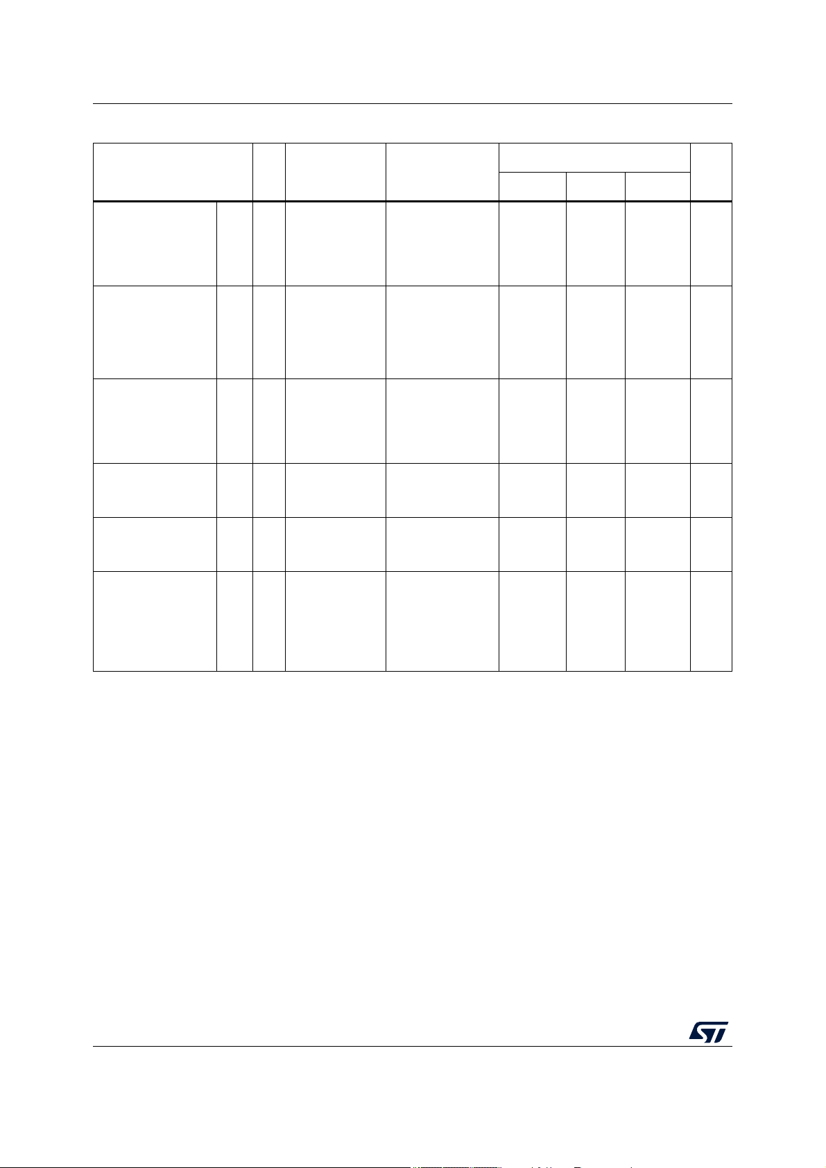
Table 1. Device summary
Part number
Package
2 MB 3 MB 4 MB
Single core Dual core Single core Dual core Single core Dual core
eTQFP64 SPC584C70E1 SPC58EC70E1 SPC584C74E1 SPC58EC74E1 SPC584C80E1 SPC58EC80E1
eTQFP100 SPC584C70E3 SPC58EC70E3 SPC584C74E3 SPC58EC74E3 SPC584C80E3 SPC58EC80E3
eTQFP144 SPC584C70E5 SPC58EC70E5 SPC584C74E5 SPC58EC74E5 SPC584C80E5 SPC58EC80E5
eLQFP176 SPC584C70E7 SPC58EC70E7 SPC584C74E7 SPC58EC74E7 SPC584C80E7 SPC58EC80E7
FPBGA292 SPC584C70C3 SPC58EC70C3 SPC584C74C3 SPC58EC74C3 SPC584C80C3 SPC58EC80C3
2/153 DS11620 Rev 7

SPC584Cx, SPC58ECx Contents
Contents
1 Introduction . . . . . . . . . . . . . . . . . . . . . . . . . . . . . . . . . . . . . . . . . . . . . . . . 6
2 Description . . . . . . . . . . . . . . . . . . . . . . . . . . . . . . . . . . . . . . . . . . . . . . . . . 7
2.1 Device feature summary . . . . . . . . . . . . . . . . . . . . . . . . . . . . . . . . . . . . . . 7
2.2 Block diagram . . . . . . . . . . . . . . . . . . . . . . . . . . . . . . . . . . . . . . . . . . . . . . . 8
2.3 Features overview . . . . . . . . . . . . . . . . . . . . . . . . . . . . . . . . . . . . . . . . . . .11
3 Package pinouts and signal descriptions . . . . . . . . . . . . . . . . . . . . . . . 13
4 Electrical characteristics . . . . . . . . . . . . . . . . . . . . . . . . . . . . . . . . . . . . 14
4.1 Introduction . . . . . . . . . . . . . . . . . . . . . . . . . . . . . . . . . . . . . . . . . . . . . . . 14
4.2 Absolute maximum ratings . . . . . . . . . . . . . . . . . . . . . . . . . . . . . . . . . . . . 15
4.3 Operating conditions . . . . . . . . . . . . . . . . . . . . . . . . . . . . . . . . . . . . . . . . 17
4.3.1 Power domains and power up/down sequencing . . . . . . . . . . . . . . . . . 19
4.4 Electrostatic discharge (ESD) . . . . . . . . . . . . . . . . . . . . . . . . . . . . . . . . . 20
4.5 Electromagnetic compatibility characteristics . . . . . . . . . . . . . . . . . . . . . . 21
4.6 Temperature profile . . . . . . . . . . . . . . . . . . . . . . . . . . . . . . . . . . . . . . . . . 22
4.7 Device consumption . . . . . . . . . . . . . . . . . . . . . . . . . . . . . . . . . . . . . . . . . 23
4.8 I/O pad specification . . . . . . . . . . . . . . . . . . . . . . . . . . . . . . . . . . . . . . . . . 26
4.8.1 I/O input DC characteristics . . . . . . . . . . . . . . . . . . . . . . . . . . . . . . . . . . 26
4.8.2 I/O output DC characteristics . . . . . . . . . . . . . . . . . . . . . . . . . . . . . . . . . 29
4.8.3 I/O pad current specifications . . . . . . . . . . . . . . . . . . . . . . . . . . . . . . . . 34
4.9 Reset pad (PORST) electrical characteristics . . . . . . . . . . . . . . . . . . . . . 37
4.10 PLLs . . . . . . . . . . . . . . . . . . . . . . . . . . . . . . . . . . . . . . . . . . . . . . . . . . . . . 40
4.10.1 PLL0 . . . . . . . . . . . . . . . . . . . . . . . . . . . . . . . . . . . . . . . . . . . . . . . . . . . 40
4.10.2 PLL1 . . . . . . . . . . . . . . . . . . . . . . . . . . . . . . . . . . . . . . . . . . . . . . . . . . . 42
4.11 Oscillators . . . . . . . . . . . . . . . . . . . . . . . . . . . . . . . . . . . . . . . . . . . . . . . . . 43
4.11.1 Crystal oscillator 40 MHz . . . . . . . . . . . . . . . . . . . . . . . . . . . . . . . . . . . . 43
4.11.2 Crystal Oscillator 32 kHz . . . . . . . . . . . . . . . . . . . . . . . . . . . . . . . . . . . . 44
4.11.3 RC oscillator 16 MHz . . . . . . . . . . . . . . . . . . . . . . . . . . . . . . . . . . . . . . . 45
4.11.4 Low power RC oscillator . . . . . . . . . . . . . . . . . . . . . . . . . . . . . . . . . . . . 46
4.12 ADC system . . . . . . . . . . . . . . . . . . . . . . . . . . . . . . . . . . . . . . . . . . . . . . . 47
4.12.1 ADC input description . . . . . . . . . . . . . . . . . . . . . . . . . . . . . . . . . . . . . . 47
DS11620 Rev 7 3/153
5

Contents SPC584Cx, SPC58ECx
4.12.2 SAR ADC 12-bit electrical specification . . . . . . . . . . . . . . . . . . . . . . . . . 48
4.12.3 SAR ADC 10-bit electrical specification . . . . . . . . . . . . . . . . . . . . . . . . . 53
4.13 Temperature Sensor . . . . . . . . . . . . . . . . . . . . . . . . . . . . . . . . . . . . . . . . . 56
4.14 LFAST pad electrical characteristics . . . . . . . . . . . . . . . . . . . . . . . . . . . . 57
4.14.1 LFAST interface timing diagrams . . . . . . . . . . . . . . . . . . . . . . . . . . . . . . 57
4.14.2 LFAST LVDS interface electrical characteristics . . . . . . . . . . . . . . . . . . 58
4.14.3 LFAST PLL electrical characteristics . . . . . . . . . . . . . . . . . . . . . . . . . . . 61
4.15 Power management . . . . . . . . . . . . . . . . . . . . . . . . . . . . . . . . . . . . . . . . . 63
4.15.1 Power management integration . . . . . . . . . . . . . . . . . . . . . . . . . . . . . . . 63
4.15.2 Voltage regulators . . . . . . . . . . . . . . . . . . . . . . . . . . . . . . . . . . . . . . . . . 69
4.15.3 Voltage monitors . . . . . . . . . . . . . . . . . . . . . . . . . . . . . . . . . . . . . . . . . . 70
4.16 Flash . . . . . . . . . . . . . . . . . . . . . . . . . . . . . . . . . . . . . . . . . . . . . . . . . . . . 73
4.17 AC Specifications . . . . . . . . . . . . . . . . . . . . . . . . . . . . . . . . . . . . . . . . . . . 77
4.17.1 Debug and calibration interface timing . . . . . . . . . . . . . . . . . . . . . . . . . 77
4.17.2 DSPI timing with CMOS pads . . . . . . . . . . . . . . . . . . . . . . . . . . . . . . . . 83
4.17.3 Ethernet timing . . . . . . . . . . . . . . . . . . . . . . . . . . . . . . . . . . . . . . . . . . . . 93
4.17.4 FlexRay timing . . . . . . . . . . . . . . . . . . . . . . . . . . . . . . . . . . . . . . . . . . . . 99
4.17.5 CAN timing . . . . . . . . . . . . . . . . . . . . . . . . . . . . . . . . . . . . . . . . . . . . . . 103
4.17.6 UART timing . . . . . . . . . . . . . . . . . . . . . . . . . . . . . . . . . . . . . . . . . . . . . 103
4.17.7 I2C timing . . . . . . . . . . . . . . . . . . . . . . . . . . . . . . . . . . . . . . . . . . . . . . . 104
5 Package information . . . . . . . . . . . . . . . . . . . . . . . . . . . . . . . . . . . . . . . 106
5.1 eTQFP64 package information . . . . . . . . . . . . . . . . . . . . . . . . . . . . . . . 106
5.1.1 Package mechanical drawings and data information . . . . . . . . . . . . . 110
5.2 eTQFP100 package information . . . . . . . . . . . . . . . . . . . . . . . . . . . . . . . 111
5.2.1 Package mechanical drawings and data information . . . . . . . . . . . . . 115
5.3 eTQFP144 package information . . . . . . . . . . . . . . . . . . . . . . . . . . . . . . .116
5.3.1 Package mechanical drawings and data information . . . . . . . . . . . . . 120
5.4 eLQFP176 package information . . . . . . . . . . . . . . . . . . . . . . . . . . . . . . . 121
5.4.1 Package mechanical drawings and data information . . . . . . . . . . . . . 125
5.5 FPBGA292 package information . . . . . . . . . . . . . . . . . . . . . . . . . . . . . . 126
5.5.1 Package mechanical drawings and data information . . . . . . . . . . . . . 128
5.6 Package thermal characteristics . . . . . . . . . . . . . . . . . . . . . . . . . . . . . . 130
5.6.1 eTQFP64 . . . . . . . . . . . . . . . . . . . . . . . . . . . . . . . . . . . . . . . . . . . . . . . 130
5.6.2 eTQFP100 . . . . . . . . . . . . . . . . . . . . . . . . . . . . . . . . . . . . . . . . . . . . . . 130
5.6.3 eTQFP144 . . . . . . . . . . . . . . . . . . . . . . . . . . . . . . . . . . . . . . . . . . . . . . 131
4/153 DS11620 Rev 7

SPC584Cx, SPC58ECx Contents
5.6.4 LQFP176 . . . . . . . . . . . . . . . . . . . . . . . . . . . . . . . . . . . . . . . . . . . . . . . 132
5.6.5 FPBGA292 . . . . . . . . . . . . . . . . . . . . . . . . . . . . . . . . . . . . . . . . . . . . . . 133
5.6.6 General notes for specifications at maximum junction temperature . . 133
6 Ordering information . . . . . . . . . . . . . . . . . . . . . . . . . . . . . . . . . . . . . . 136
7 Revision history . . . . . . . . . . . . . . . . . . . . . . . . . . . . . . . . . . . . . . . . . . 140
DS11620 Rev 7 5/153
5

Introduction SPC584Cx, SPC58ECx
1 Introduction
This document describes the features of the family and options available within the family
members, and highlights important electrical and physical characteristics of the device. To
ensure a complete understanding of the device functionality, refer also to the device
reference manual and errata sheet.
6/153 DS11620 Rev 7
SPC584Cx, SPC58ECx Description
2 Description
The SPC584Cx and SPC58ECx microcontroller is the first in a new family of devices
superseding the SPC564Cx and SPC56ECx family. SPC584Cx and SPC58ECx builds on
the legacy of the SPC564Cx and SPC56ECx family, while introducing new features coupled
with higher throughput to provide substantial reduction of cost per feature and significant
power and performance improvement (MIPS per mW). On the SPC584Cx and SPC58ECx
device, there are two processor cores e200z420 and one e200z0 core embedded in the
Hardware Security Module.
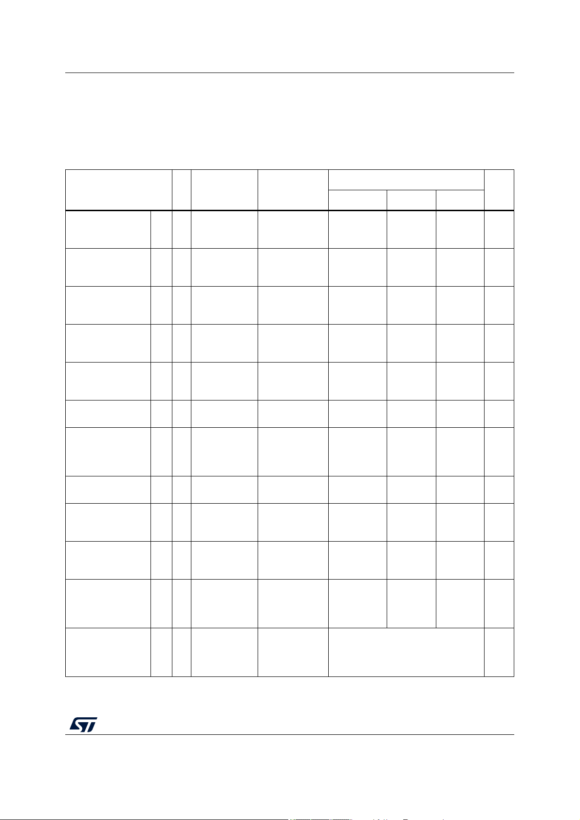
2.1 Device feature summary
Table 2 lists a summary of major features for the SPC584Cx and SPC58ECx device. The
feature column represents a combination of module names and capabilities of certain
modules. A detailed description of the functionality provided by each on-chip module is
given later in this document.
Feature Description
Table 2. Features List
SPC58 family 40 nm
Number of Cores 2
Local RAM 2x 64 KB Data
Single Precision Floating Point Yes
SIMD No
VLE Yes
Cache
MPU
Semaphores Yes
CRC Channels 2 x 4
Software Watchdog Timer (SWT) 3
Core Nexus Class 3+
Event Processor
Run control Module Yes
System SRAM 384 KB (including 256 KB of standby RAM)
8 KB Instruction
4 KB Data
Core MPU: 24 per CPU
System MPU: 24 per XBAR
4 x SCU
4 x PMC
Flash 4096 KB code / 128 KB data
Flash fetch accelerator 2 x 4 x 256-bit
DMA channels 64
DS11620 Rev 7 7/153
12
Description SPC584Cx, SPC58ECx
Table 2. Features List (continued)
Feature Description
DMA Nexus Class 3
LINFlexD 18
MCAN (ISO CAN-FD compliant) 8
DSPI 8
I2C 1
FlexRay 1 x Dual channel
Ethernet 1 MAC with Time Stamping, AVB and VLAN support
SIPI / LFAST Debugger High Speed
8 PIT channels
System Timers
eMIOS 2 x 32 channels
BCTU 64 channels
Interrupt controller 1 x 568 sources
ADC (SAR) 5
4 AUTOSAR® (STM)
RTC/API
Temp. sensor Yes
Self Test Controller Yes
PLL Dual PLL with FM
Integrated linear voltage regulator Yes
External Power Supplies 5 V, 3.3 V
Low Power Modes
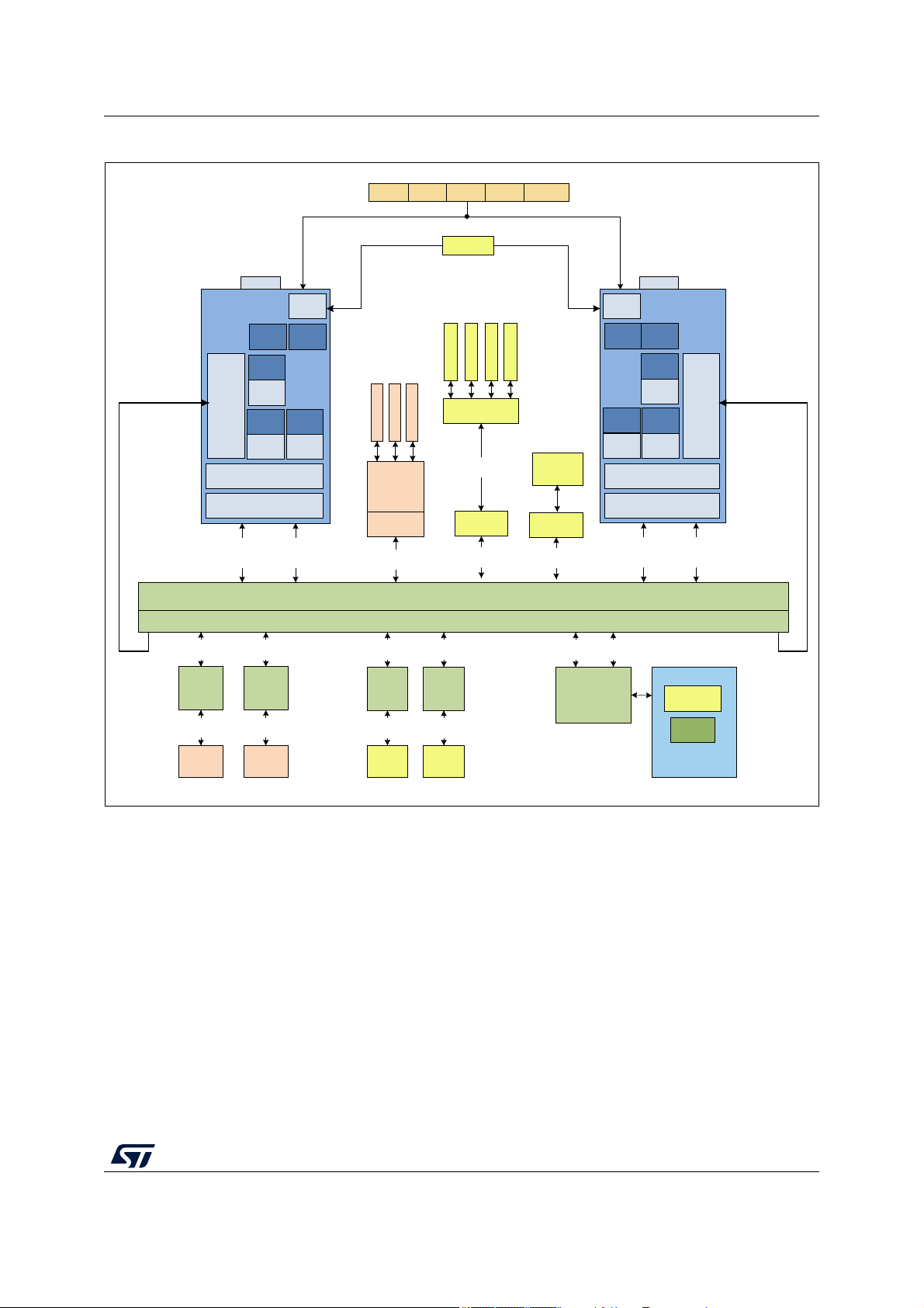
2.2 Block diagram
The figures below show the top-level block diagrams.
HALT Mode
STOP Mode
Smart Standby with output controller, analog and digital inputs
Standby Mode
8/153 DS11620 Rev 7
SPC584Cx, SPC58ECx Description
Delayed Lock-step with Redundancy Checkers
Delayed Lock-step with Redundancy Checkers
Instruction
32 ADD
64 DATA
Load / Store
32 ADD
64 DATA
M4
M5
FLASH
4 MB
EEPROM
4x32 KB
Non Volatile Memory
Multiple RWW partitions
256 Page Line
EFPU2VLE
Core Memory Protection Unit
(CMPU)
e200 z420n3
– 180 MHz
dual issue
Main Core_0
Nexus3p
BIU with E2E ECC
Decorated Storage Access
SWT_0 IAC
S5
System Memory Protection Unit
Cross Bar Switch (XBAR) AMBA 2.0 v6 AHB – 64 bits
Unified
Backdoor
Interface
With
E2E ECC
S7
Periph.
Bridge 2
E2E ECC
Peripheral
Cluster 2
32 ADD
64 DATA
32 ADD
32 DATA
Periph.
Bridge 1
E2E ECC
Peripheral
Cluster 1
32 ADD
64 DATA
32 ADD
32 DATA
PRAMC_3
with E2E
ECC
32 ADD
64 DATA
SRAM
Array 3
128 KB
32 ADD
64 DATA
PRAMC_2
with E2E
ECC
32 ADD
64 DATA
SRAM
Array 2
256 KB
32 ADD
64 DATA
PFLASHC_1
Set-Associative Prefetch
Buffers
with E2E ECC
32 ADD
64 DATA
S4
S2 S0
S1
S6
M0 M1
S3
SPUDCIJTAGCJTAGM NPC
32 ADD
64 DATA
FlexRay_0
M3
Nexus Data
Trace
ETHERNET_0
Nexus Data
Trace
HSM
32 ADD
64 DATA
32 ADD
64 DATA
M2
Concentrator_1
E2E ECC
PAMU
SWT_2 IAC
Delayed Lock-step with Redundancy Checkers
Instruction
32 ADD
64 DATA
Load / Store
32 ADD
64 DATA
e200 z420n3 – 180 MHz
dual issue
Main Core_2
Nexus3p
VLE EFPU2
Unified
Backdoor
Interface
With
E2E ECC
Core Memory Protection Unit
(CMPU)
BIU with E2E ECC
Decorated Storage Access
INTC
I-Cache
Control
8 KB
2 way
D-MEM
Control
64 KB
D-MEM
D-Cache
Control
4 KB
2 way
I-Cache
Control
8 KB
2 way
D-MEM
Control
64 KB
D-MEM
D-Cache
Control
4 KB
2 way
SIPI_1
Nexus Data
Trace
32 ADD
64 DATA
M6
32 ADD
64 DATA
DMA CHMUX_1
64 Ch
eDMA_1
DMA CHMUX_2
DMA CHMUX_0
DMA CHMUX_3
Figure 1. Block diagram
DS11620 Rev 7 9/153
12
Description SPC584Cx, SPC58ECx
Note:
In this diagram, ON-platform modules are shown in orange color and OFF-platform modules
are shown in blue color.
3%5,'*(B±3HULSKHUDO&OXVWHU
3%5,'*(B±3HULSKHUDO&OXVWHU
%&78B
H0,26B
3%5,'*(B
;%$5B
;%,&B&RQFHQWUDWRUB
6038B
;%,&B
3&0B
3)/$6+B
6(0
,17&B
6:7B
670B
H'0$B
35$0B
7'0B
67'%<B&78B
H0,26B
(7+(51(7B
6$5B$'&BELWB
6$5B$'&BELWB67'%<
6$5B$'&BELWB%
)/(;5$<B
,&B
'63,B
/,1)OH['B
&$1B68%BB0(66$*(B5$0
&$1B68%BB0B&$1B
&&&8
+60
'76
-'&
67&8
-7$*0
0(08
,0$
&5&B
'0$08;B
3,7B
57&$3,
:.38
0&B3&8
30&B',*
0&B5*0
5&26&B',*
5&.B',*
26&B',*
26&.B',*
3//B',*
&08BB3//B;26&B,5&26&
0&B&*0
0&B0(
6,8/
)/$6+B
)/$6+B$/7B
3$66
66&0
3%5,'*(B
6$5B$'&BELWB
'63,B
/,1)OH['B
&$1B68%BB0(66$*(B5$0
&$1B68%BB0B&$1B
)&&8
&5&B
'0$08;B
3,7B
&08BB&25(B;%$5
&08BB+3%0
&08BB3%5,'*(
&08BB6$5$'&
&08BB)%5,'*(
&08BB(0,26
&08BB3)%5,'*(
6,3,B
/)$67B
Figure 2. Periphery allocation
10/153 DS11620 Rev 7

SPC584Cx, SPC58ECx Description
2.3 Features overview
On-chip modules within SPC584Cx and SPC58ECx include the following features:
• Two main CPUs, dual issue, 32-bit CPU core complexes (e200z4).
– Power Architecture embedded specification compliance
– Instruction set enhancement allowing variable length encoding (VLE), encoding a
mix of 16-bit and 32-bit instructions, for code size footprint reduction
– Single-precision floating point operations
– 64 KB local data RAM for Core_0 and Core_2
– 8 KB I-Cache and 4 KB D-Cache for Core_0 and Core_2
• 4224 KB (4096 KB code flash + 128 KB data flash) on-chip flash memory
– Supports read during program and erase operations, and multiple blocks allowing
EEPROM emulation
• 176 KB HSM dedicated flash memory (144 KB code + 32 KB data)
• 384 KB on-chip general-purpose SRAM (+ 128 KB local data RAM: 64 KB included in
each CPU)
• Multi channel direct memory access controllers
– 64 eDMA channels
• One interrupt controller (INTC)
• Dual phase-locked loops with stable clock domain for peripherals and FM modulation
domain for computational shell
• Crossbar switch architecture for concurrent access to peripherals, Flash, or RAM from
multiple bus masters with end-to-end ECC
• Hardware security module (HSM) with HW cryptographic co-processor
• System integration unit lite (SIUL)
• Boot assist Flash (BAF) supports factory programming using a serial bootload through the
asynchronous CAN or LIN/UART.
• Hardware support for safety ASIL-B level related applications
• Enhanced modular IO subsystem (eMIOS): up to 64 (2 x 32) timed I/O channels with
16-bit counter resolution
– Buffered updates
– Support for shifted PWM outputs to minimize occurrence of concurrent edges
– Supports configurable trigger outputs for ADC conversion for synchronization to
channel output waveforms
– Shared or independent time bases
– DMA transfer support available
• Body cross triggering unit (BCTU)
– Triggers ADC conversions from any eMIOS channel
– Triggers ADC conversions from up to 2 dedicated PIT_RTIs
– One event configuration register dedicated to each timer event allows to define the
corresponding ADC channel
– Synchronization with ADC to avoid collision
DS11620 Rev 7 11/153
12

Description SPC584Cx, SPC58ECx
• Enhanced analog-to-digital converter system with:
– Three independent fast 12-bit SAR analog converters
– One supervisor 12-bit SAR analog converter
– One 10-bit SAR analog converter with STDBY mode support
• Eight deserial serial peripheral interface (DSPI) modules
• Eighteen LIN and UART communication interface (LINFlexD) modules
– LINFlexD_0 is a Master/Slave
– All others are Masters
• Eight modular controller area network (MCAN) modules, all supporting flexible data rate
(ISO CAN-FD compliant)
• Dual-channel FlexRay controller
• One ethernet controller 10/100 Mbps, compliant IEEE 802.3-2008
– IEEE 1588-2008 Time stamping (internal 64-bit time stamp)
– IEEE 802.1AS and IEEE 802.1Qav (AVB-Feature)
– IEEE 802.1Q VLAN tag detection
– IPv4 and IPv6 checksum modules
• Nexus development interface (NDI) per IEEE-ISTO 5001-2003 standard, with some
support for 2010 standard.
• Device and board test support per Joint Test Action Group (JTAG) (IEEE 1149.1 and
IEEE 1149.7), 2-pin JTAG interface.
• Standby power domain with smart wake-up sequence
12/153 DS11620 Rev 7

SPC584Cx, SPC58ECx Package pinouts and signal descriptions
3 Package pinouts and signal descriptions
Refer to the SPC584Cx and SPC58ECx IO_ Definition document.
It includes the following sections:
1. Package pinouts
2. Pin descriptions
a) Power supply and reference voltage pins
b) System pins
c) LVDS pins
d) Generic pins
DS11620 Rev 7 13/153
13
Electrical characteristics SPC584Cx, SPC58ECx
4 Electrical characteristics
4.1 Introduction
The present document contains the target Electrical Specification for the 40 nm family 32-bit
MCU SPC584Cx and SPC58ECx products.
In the tables where the device logic provides signals with their respective timing
characteristics, the symbol “CC” (Controller Characteristics) is included in the “Symbol”
column.
In the tables where the external system must provide signals with their respective timing
characteristics to the device, the symbol “SR” (System Requirement) is included in the
“Symbol” column.
The electrical parameters shown in this document are guaranteed by various methods. To
give the customer a better understanding, the classifications listed in Table 3 are used and
the parameters are tagged accordingly in the tables where appropriate.
Classification tag Tag description
Table 3. Parameter classifications
P Those parameters are guaranteed during production testing on each individual device.
C Those parameters are achieved by the design characterization by measuring a statistically
relevant sample size across process variations.
T Those parameters are achieved by design validation on a small sample size from typical
devices.
D Those parameters are derived mainly from simulations.
14/153 DS11620 Rev 7
SPC584Cx, SPC58ECx Electrical characteristics
4.2 Absolute maximum ratings
Table 4 describes the maximum ratings for the device. Absolute maximum ratings are stress
ratings only, and functional operation at the maxima is not guaranteed. Exposure to
absolute maximum rating conditions for extended periods may affect device reliability.
Stress beyond the listed maxima, even momentarily, may affect device reliability or cause
permanent damage to the device.
Symbol C Parameter Conditions
V
DD_LV
V
DD_HV_IO_MAIN
V
DD_HV_IO_FLEX
V
DD_HV_OSC
V
DD_HV_FLA
V
SS_HV_ADV
V
DD_HV_ADV
V
SS_HV_ADR_S
SR D
SR D
SR D
SR D
SR D
Table 4. Absolute maximum ratings
Core voltage
operating life
(1)
range
I/O supply
voltage
(2)
ADC ground
voltage
ADC Supply
voltage
(2)
SAR ADC
ground
reference
— –0.3 — 1.4 V
— –0.3 — 6.0 V
Reference to
digital ground
Reference to
V
SS_HV_ADV
— –0.3 — 0.3 V
Value
Unit
Min Typ Max
–0.3 — 0.3 V
–0.3 — 6.0 V
V
DD_HV_ADR_S
V
SS-VSS_HV_ADR_S
V
SS-VSS_HV_ADV
V
IN
T
TRIN
I
INJ
SR D
SR D
SR D
SR D
SR D
SR T
SAR ADC
voltage
reference
V
SS_HV_ADR_S
(2)
differential
voltage
V
SS_HV_ADV
differential
voltage
I/O input voltage
(2)(3) (4)
range
Digital Input pad
transition time
(5)
Maximum DC
injection current
for each
analog/digital
PAD
(6)
Reference to
V
SS_HV_ADR_S
–0.3 — 6.0 V
— –0.3 — 0.3 V
— –0.3 — 0.3 V
— –0.3 — 6.0
Relative to V
Relative to
V
DD_HV_IO
V
DD_HV_ADV
and
ss
–0.3 — —
V
——0.3
———1ms
—–5—5mA
DS11620 Rev 7 15/153
16
Electrical characteristics SPC584Cx, SPC58ECx
Table 4. Absolute maximum ratings (continued)
Value
Symbol C Parameter Conditions
Maximum non-
operating
T
STG
SR T
Storage
— –55 — 125 °C
temperature
range
Maximum non-
operating
T
PAS
SR C
temperature
—–55—150
during passive
lifetime
Min Typ Max
(7)
Unit
°C
T
STORAGE
SR —
Maximum
storage time,
assembled part
programmed in
ECU
No supply; storage
temperature in
range –40 °C to
60 °C
— — 20 years
Maximum solder
T
SDR
SR T
temperature Pbfree packaged
(8)
———260°C
Moisture
MSL SR T
sensitivity
(9)
level
———3—
Typical range for
X-rays source
during
inspection:80 ÷
130 KV; 20 ÷
—— 1grey
dose SR T
T
XRAY
Maximum
cumulated
XRAY dose
50 μA
1. V
2. V
3. The maximum input voltage on an I/O pin tracks with the associated I/O supply maximum. For the injection current
4. Relative value can be exceeded if design measures are taken to ensure injection current limitation (parameter IINJ).
5. This limitation applies to pads with digital input buffer enabled. If the digital input buffer is disabled, there are no maximum
6. The limits for the sum of all normal and injected currents on all pads within the same supply segment can be found in
7. 175°C are allowed for limited time. Mission profile with passive lifetime temperature >150°C have to be evaluated by ST to
8. Solder profile per IPC/JEDEC J-STD-020D.
9. Moisture sensitivity per JDEC test method A112.
: allowed 1.335 V - 1.400 V for 60 seconds cumulative time at the given temperature profile. Remaining time allowed
DD_LV
1.260 V - 1.335 V for 10 hours cumulative time at the given temperature profile. Remaining time as defined in Section 4.3:
Operating conditions.
: allowed 5.5 V – 6.0 V for 60 seconds cumulative time at the given temperature profile, for 10 hours cumulative
DD_HV
time with the device in reset at the given temperature profile. Remaining time as defined in Section 4.3: Operating
conditions.
condition on a pin, the voltage will be equal to the supply plus the voltage drop across the internal ESD diode from I/O pin
to supply. The diode voltage varies greatly across process and temperature, but a value of 0.3 V can be used for nominal
calculations.
limits to the transition time.
Section 4.8.3: I/O pad current specifications.
confirm that are granted by product qualification.
16/153 DS11620 Rev 7
SPC584Cx, SPC58ECx Electrical characteristics
4.3 Operating conditions
Table 5 describes the operating conditions for the device, and for which all the specifications
in the data sheet are valid, except where explicitly noted. The device operating conditions
must not be exceeded or the functionality of the device is not guaranteed.
Symbol C Parameter Conditions
Table 5. Operating conditions
(1)
Value
Min Typ Max
Unit
(2)
F
SYS
T
A_125 Grade
T
J_125 Grade
T
A_105 Grade
T
J_105 Grade
V
DD_LV
V
DD_HV_IO_MAIN
V
DD_HV_IO_FLEX
V
DD_HV_FLA
V
DD_HV_OSC
V
DD_HV_ADV
(4)
(4)
(4)
(4)
SR P
SR D
SR P
SR D
SR D
SR P
SR P
SR P
Operating
system clock
frequency
(3)
Operating
Ambient
temperature
Junction
temperature
under bias
Ambient
temperature
under bias
Operating
Junction
temperature
Core supply
voltage
(5)
IO supply
voltage
ADC supply
voltage
———180MHz
— –40 — 125 °C
TA= 125 °C –40 — 150 °C
— –40 — 105 °C
TA= 105 °C –40 — 130 °C
— 1.14 1.20 1.26
(6) (7)
V
— 3.0 — 5.5 V
— 3.0 — 5.5 V
V
SS_HV_ADV
V
SS
V
DD_HV_ADR_S
V
DD_HV_ADR_S
V
DD_HV_ADV
V
SS_HV_ADR_S
SR D
ADC ground
differential
— –25 — 25 mV
voltage
SAR ADC
SR P
reference
— 3.0 — 5.5 V
voltage
SAR ADC
SR D
reference
differential
———25mV
voltage
SAR ADC
SR P
ground
reference
—V
SS_HV_ADV
V
voltage
DS11620 Rev 7 17/153
19
Electrical characteristics SPC584Cx, SPC58ECx
Table 5. Operating conditions (continued)
(1)
Value
Symbol C Parameter Conditions
Min Typ Max
Unit
V
SS_HV_ADR_S
V
SS_HV_ADV
SR D
V
SS_HV_ADR_S
differential
voltage
— –25 — 25 mV
Slew rate on
V
RAMP_HV
SR D
HV power
———100V/ms
supply
V
IN
SR P
I/O input
voltage range
—0—5.5V
Injection
current (per
I
INJ1
SR T
pin) without
performance
degradation
(9) (10)
Digital pins and
analog pins
(8)
–3.0 — 3.0 mA
Dynamic
Injection
current (per
I
INJ2
SR D
pin) with
performance
degradation
(11)
1. The ranges in this table are design targets and actual data may vary in the given range.
2. The maximum number of PRAM wait states has to be configured accordingly to the system clock frequency. Refer to
Table 6.
3. Maximum operating frequency is applicable to the cores and platform of the device. See the Clock Chapter in the
Microcontroller Reference Manual for more information on the clock limitations for the various IP blocks on the device.
4. In order to evaluate the actual difference between ambient and junction temperatures in the application, refer to
Section 5.6: Package thermal characteristics.
5. Core voltage as measured on device pin to guarantee published silicon performance.
6. Core voltage can exceed 1.26 V with the limitations provided in Section 4.2: Absolute maximum ratings, provided that
HVD134_C monitor reset is disabled.
7. 1.260 V - 1.290 V range allowed periodically for supply with sinusoidal shape and average supply value below or equal to
1.236 V at the given temperature profile.
8. Full device lifetime. I/O and analog input specifications are only valid if the injection current on adjacent pins is within these
limits. See Section 4.2: Absolute maximum ratings for maximum input current for reliability requirements.
9. The I/O pins on the device are clamped to the I/O supply rails for ESD protection. When the voltage of the input pins is
above the supply rail, current will be injected through the clamp diode to the supply rails. For external RC network
calculation, assume typical 0.3 V drop across the active diode. The diode voltage drop varies with temperature.
10. The limits for the sum of all normal and injected currents on all pads within the same supply segment can be found in
Section 4.8.3: I/O pad current specifications.
11. Positive and negative Dynamic current injection pulses are allowed up to this limit. I/O and ADC specifications are not
granted. See the dedicated chapters for the different specification limits. See the Absolute Maximum Ratings table for
maximum input current for reliability requirements. Refer to the following pulses definitions: Pulse1 (ISO 7637-2:2011),
Pulse 2a(ISO 7637-2:2011 5.6.2), Pulse 3a (ISO 7637-2:2011 5.6.3), Pulse 3b (ISO 7637-2:2011 5.6.3).
Digital pins and
analog pins
(10)
–10 — 10 mA
18/153 DS11620 Rev 7
SPC584Cx, SPC58ECx Electrical characteristics
Table 6. PRAM wait states configuration
PRAMC WS Clock Frequency (MHz)
1<
0<
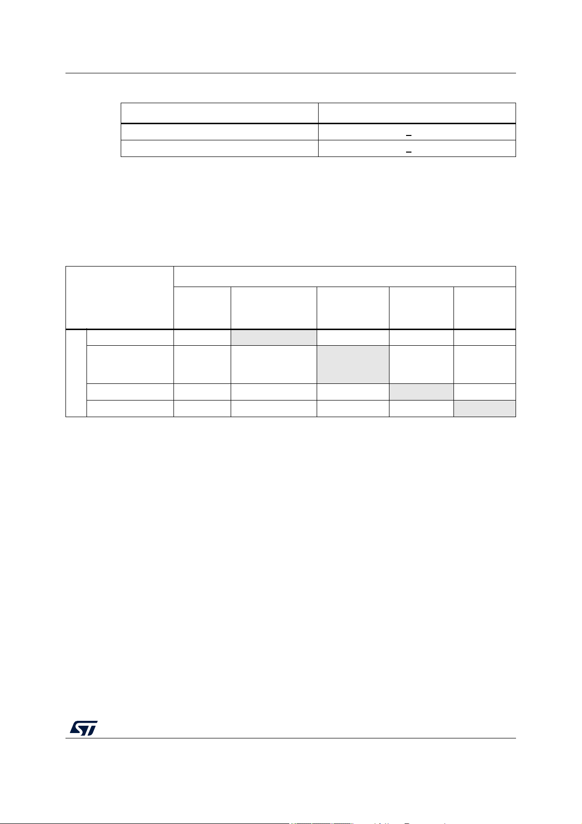
4.3.1 Power domains and power up/down sequencing
The following table shows the constraints and relationships for the different power domains.
Supply1 (on rows) can exceed Supply2 (on columns), only if the cell at the given row and
column is reporting ‘ok’. This limitation is valid during power-up and power-down phases, as
well as during normal device operation.
Table 7. Device supply relation during power-up/power-down sequence
Supply2
V
DD_HV_IO_MAIN
V
DD_HV_FLA
V
DD_HV_OSC
V
V
Supply1
DD_HV_IO_FLEX
DD_HV_IO_MAIN
V
DD_HV_FLA
V
DD_HV_OSC
V
DD_HV_ADV
V
DD_HV_ADR
V
DD_LV
V
DD_HV_IO_FLEX
ok not allowed ok ok
ok ok ok ok
ok ok not allowed ok
ok ok not allowed not allowed
180
120
V
DD_HV_ADV
V
DD_HV_ADR
During power-up, all functional terminals are maintained in a known state as described in
the device pinout Microsoft Excel file attached to the IO_Definition document.
DS11620 Rev 7 19/153
19
Electrical characteristics SPC584Cx, SPC58ECx
4.4 Electrostatic discharge (ESD)
The following table describes the ESD ratings of the device:
• All ESD testing are in conformity with CDF-AEC-Q100 Stress Test Qualification for
Automotive Grade Integrated Circuits,
• Device failure is defined as: “If after exposure to ESD pulses, the device does not meet
the device specification requirements, which include the complete DC parametric and
functional testing at room temperature and hot temperature, maximum DC parametric
variation within 10% of maximum specification”.
Parameter C Conditions Value Unit
ESD for Human Body Model (HBM)
ESD for field induced Charged Device Model (CDM)
1. This parameter tested in conformity with ANSI/ESD STM5.1-2007 Electrostatic Discharge Sensitivity Testing.
2. This parameter tested in conformity with ANSI/ESD STM5.3-1990 Charged Device Model - Component Level.
(1)
Table 8. ESD ratings
T All pins 2000 V
(2)
T All pins 500 V
T Corner Pins 750 V
20/153 DS11620 Rev 7

SPC584Cx, SPC58ECx Electrical characteristics
4.5 Electromagnetic compatibility characteristics
EMC measurements at IC-level IEC standards are available from STMicroelectronics on
request.
DS11620 Rev 7 21/153
21

Electrical characteristics SPC584Cx, SPC58ECx
4.6 Temperature profile
The device is qualified in accordance to AEC-Q100 Grade1 requirements, such as HTOL
1,000 h and HTDR 1,000 hrs, T
Mission profile exceeding AEC-Q100 Grade 1, and with junction Temperature equal to or
lower than 150 °C have to be evaluated by ST to confirm that are covered by product
qualification. Contact your STMicroelectronics Sales representative for validation.
=150°C.
J
22/153 DS11620 Rev 7
SPC584Cx, SPC58ECx Electrical characteristics
4.7 Device consumption
Symbol C Parameter Conditions
I
I
DD_MAIN_CORE_AC
(2),(3)
DD_LKG
(3)
I
DD_LV
I
DD_HV
I
DD_LV_GW
I
DD_HV_GW
I
DD_LV_BCM
I
DD_HV_BCM
I
DD_HSM_AC
Table 9. Device consumption
C
DT
DT
CC
Leakage current on the
V
supply
DT
DD_LV
DT
PT
Dynamic current on
CC P
CC P
the V
very high consumption
Total current on the
V
DD_HV
DD_LV
profile
supply
supply,
(4)
(4)
Dynamic current on
CC T
the V
DD_LV
supply,
gateway profile
(5)
Dynamic current on
CC T
the V
DD_HV
supply,
gateway profile
(5)
Dynamic current on
CC T
the V
DD_LV
body profile
supply,
(6)
Dynamic current on
CC T
CC T
CC T
the V
body profile
Main Core dynamic
HSM platform dynamic
operating current
DD_HV
current
supply,
(6)
(7)
(8)
=40°C — — 14
T
J
=25°C — — 10
J
=55°C — — 20
J
=95°C — — 50
J
= 120 °C — — 90
J
= 150 °C — — 180
J
— — — 210 mA
f
MAX
— — — 170 mA
———37mA
— — — 150 mA
———44mA
f
MAX
f
/2 — — 20 mA
MAX
(1)
Value
Unit
Min Typ Max
mA
——64mA
——50mA
I
DDHALT
I
DDSTOP
(9)
(10)
CC T
CC T
Dynamic current on
DD_LV
supply
the V
+Total current on the
DD_HV
supply
V
Dynamic current on
DD_LV
supply
the V
+Total current on the
DD_HV
supply
V
DS11620 Rev 7 23/153
— — 71 100 mA
— — 15 30 mA
25
Electrical characteristics SPC584Cx, SPC58ECx
Table 9. Device consumption (continued)
(1)
Value
Symbol C Parameter Conditions
Min Typ Max
Unit
I
DDSTBY8
I
DDSTBY32
I
DDSTBY256
D
Total standby mode
CC
current on V
DT
V
DT
DD_HV
RAM
supply, 8 KB
DD_LV
(11)
and
PT
D
Total standby mode
CC
V
supply, 32 KB
DD_HV
DT
RAM
current on V
DT
DD_LV
(11)
and
PT
D
Total standby mode
CC
DT
V
DD_HV
256 KB RAM
current on V
DT
DD_LV
supply,
(11)
and
PT
TJ= 25 °C — 85 160
= 40 °C — — 250
J
= 55 °C — — 370
J
= 120 °C — 1.2 2.2
J
= 150 °C — 2.9 5.0
J
TJ= 25 °C — 100 180
= 40 °C — — 270
J
= 55 °C — — 410
J
= 120 °C — — 2.4
J
= 150 °C — — 5.5
J
TJ= 25 °C — 150 250
= 40 °C — — 390
J
= 55 °C — — 590
J
= 120 °C — 2.0 3.5 mA
J
= 150 °C — 5.1 8
J
µACT
mA
µACT
mA
µACT
SSWU running over all
STANDBY period with
I
DDSSWU1
CC D
OPC/TU commands
execution and keeping
ADC off
(12)
TJ=40°C — 1.0 3.5 mA
SSWU running over all
STANDBY period with
I
DDSSWU2
1. The ranges in this table are design targets and actual data may vary in the given range.
2. The leakage considered is the sum of core logic and RAM memories. The contribution of analog modules is not considered,
and they are computed in the dynamic I
3. I
4. Use case: 2 x e200Z4 @180 MHz, HSM @90 MHz, all IPs clock enabled, Flash access with prefetch disabled, Flash
5. Gateway use case: Two cores running at 160 MHz, DMA, PLL, FLASH read only 25%, 8xCAN, 1xEthernet, HSM,
6. BCM use case: One Core running at 160 MHz, no lockstep no, DMA, PLL, FLASH read only 25%, 2xCAN, HSM,
(leakage current) and I
DD_LKG
consumption contributors. The tests used in validation, characterization and production are verifying that the total
consumption (leakage+dynamic) is lower or equal to the sum of the maximum values provided (I
parameters, measured separately, may exceed the maximum reported for each, depending on the operative conditions and
the software profile used.
consumption includes parallel read and program/erase, all SARADC in continuous conversion, DMA continuously triggered
by ADC conversion, 4 DSPI / 8 CAN / 2 LINFlex and 2 DSPI transmitting, 2 x EMIOS running (8 channels in OPWMT
mode), FIRC, SIRC, FXOSC, PLL0-1 running. The switching activity estimated for dynamic consumption does not include
I/O toggling, which is highly dependent on the application. Details of the software configuration are available separately.
The total device consumption is I
2xSARADC.
4xSARADC.
CC D
(dynamic current) are reported as separate parameters, to give an indication of the
DD_LV
DD_LV
OPC/TU/ADC
commands execution
and keeping ADC
DD_LV
+ I
DD_HV
and I
+ I
(13)
on
DD_HV
DD_LKG
parameters.
TJ=40°C — 3.5 5.0 mA
for the selected temperature.
DD_LKG+IDD_LV
). The two
24/153 DS11620 Rev 7

SPC584Cx, SPC58ECx Electrical characteristics
7. Dynamic consumption of one core, including the dedicated I/D-caches and I/D-MEMS contribution.
8. Dynamic consumption of the HSM module, including the dedicated memories, during the execution of Electronic Code
Book crypto algorithm on 1 block of 16 byte of shared RAM.
9. Flash in Low Power. Sysclk at 160 MHz, PLL0_PHI at 160 MHz, XTAL at 40 MHz, FIRC 16 MHz ON, RCOSC1M off.
FlexCAN: instances: 0, 1, 2, 3, 4, 5, 6, 7 ON (configured but no reception or transmission), Ethernet ON (configured but no
reception or transmission), ADC ON (continuously converting). All others IPs clock-gated.
10. Sysclk = RC16 MHz, RC16 MHz ON, RC1 MHz ON, PLL OFF. All possible peripherals off and clock gated. Flash in power
down mode.
11. STANDBY mode: device configured for minimum consumption, RC16 MHz off, RC1 MHz on, OSC32K off, SSWU off.
12. SSWU1 mode adder: FIRC = ON, SSWU clocked at 8 MHz and running over all STANDBY period, ADC off. The total
standby consumption can be obtained by adding this parameter to the IDDSTBY parameter for the selected memory size
and temperature.
13. SSWU2 mode adder: FIRC = ON, SSWU clocked at 8 MHz and running over all STANDBY period, ADC on in continuous
conversion. The total standby consumption can be obtained by adding this parameter to the I
selected memory size and temperature.
parameter for the
DDSTBY
DS11620 Rev 7 25/153
25
Electrical characteristics SPC584Cx, SPC58ECx
4.8 I/O pad specification
The following table describes the different pad type configurations.
Pad type Description
Weak configuration Provides a good compromise between transition time and low electromagnetic emission.
Medium configuration
Strong configuration Provides fast transition speed; used for fast interface.
Very strong
configuration
Table 10. I/O pad specification descriptions
Provides transition fast enough for the serial communication channels with controlled
current to reduce electromagnetic emission.
Provides maximum speed and controlled symmetric behavior for rise and fall transition.
Used for fast interface including Ethernet and FlexRay interfaces requiring fine control of
rising/falling edge jitter.
Differential
configuration
Input only pads These low input leakage pads are associated with the ADC channels.
Standby pads
A few pads provide differential capability providing very fast interface together with good
EMC performances.
These pads (LP pads) are active during STANDBY. They are configured in CMOS level
logic and this configuration cannot be changed. Moreover, when the device enters the
STANDBY mode, the pad-keeper feature is activated for LP pads. It means that:
– if the pad voltage level is above the pad keeper high threshold, a weak pull-up resistor
is automatically enabled
– if the pad voltage level is below the pad keeper low threshold, a weak pull-down resistor
is automatically enabled.
For the pad-keeper high/low thresholds please consider (VDD_HV_IO_MAIN / 2) +/-20%.
Note: Each I/O pin on the device supports specific drive configurations. See the signal description
table in the device reference manual for the available drive configurations for each I/O pin.
PMC_DIG_VSIO register has to be configured to select the voltage level (3.3 V or 5.0 V) for
each IO segment.
Logic level is configurable in running mode while it is CMOS not-configurable in STANDBY
for LP (low power) pads, so if a LP pad is used to wakeup from STANDBY, it should be
configured as CMOS also in running mode in order to prevent device wrong behavior in
STANDBY.
4.8.1 I/O input DC characteristics
The following table provides input DC electrical characteristics, as described in Figure 3.
26/153 DS11620 Rev 7
SPC584Cx, SPC58ECx Electrical characteristics
V
IL
V
IN
V
IH
V
INTERNAL
V
DD
V
HYS
(SIUL register)
Figure 3. I/O input electrical characteristics
Table 11. I/O input electrical characteristics
Symbol C Parameter Conditions
V
V
V
hysttl
V
ihcmos
V
ilcmos
V
hyscmos
ihttl
ilttl
SR P
SR P
CC C
SR P
SR P
CC C
Input high level
TTL
Input low level
TTL
Input hysteresis
TTL
Input high level
CMOS
Input low level
CMOS
Input hysteresis
CMOS
Value
Unit
Min Typ Max
TTL
V
—2—
DD_HV_IO
+ 0.3
V
— –0.3 — 0.8 V
—0.3——V
CMOS
DD
V
V
V
—0.65 * V
DD
—
DD_HV_IO
+ 0.3
— –0.3 — 0.35 * V
—0.10 * VDD——V
COMMON
I
LKG
I
LKG
I
LKG
CC P
CC P
CC P
Pad input
leakage
Pad input
leakage
Pad input
leakage
INPUT-ONLY pads
=150°C
T
J
STRONG pads
=150°C
T
J
VERY STRONG pads,
T
=150°C
J
——200nA
— — 1,000 nA
— — 1,000 nA
DS11620 Rev 7 27/153
36
Electrical characteristics SPC584Cx, SPC58ECx
Table 11. I/O input electrical characteristics (continued)
Value
Symbol C Parameter Conditions
Min Typ Max
Unit
C
P1
V
drift
W
FI
CC D
CC D
SR C
Pad
capacitance
Input Vil/Vih
temperature
drift
Wakeup input
filtered pulse
———10pF
In a 1 ms period, with a
temperature variation
<30 °C
(1)
———20ns
——100mV
Wakeup input
W
NFI
1. In the range from WFI (max) to W
voltage. Refer to the device pinout IO definition excel file for the list of pins supporting the wakeup filter feature.
SR C
not filtered
(1)
pulse
(min), pulses can be filtered or not filtered, according to operating temperature and
NFI
— 400 — — ns
Table 12. I/O pull-up/pull-down electrical characteristics
Value
Symbol C Parameter Conditions
Min Typ Max
(1)
= 0.69 *
(2)
= 5.0 V ±
10%
——130
15 — —
33 — 93 KΩ
I
WPU
R
WPU
CC
CC D
T
Weak pull-up
current
P
absolute value
Weak Pull-up
resistance
V
IN
V
IN
V
DD_HV_IO
V
DD_HV_IO
= 1.1 V
Unit
μA
R
I
WPD
WPU
CC D
CC
Weak Pull-up
resistance
T
Weak pull-
down current
absolute value
P
Weak Pull-
R
WPD
CC D
down
resistance
Weak Pull-
R
WPD
CC D
down
resistance
1. Maximum current when forcing a change in the pin level opposite to the pull configuration.
2. Minimum current when keeping the same pin level state than the pull configuration.
V
DD_HV_IO
VIN = 0.69 *
V
DD_HV_IO
VIN = 0.9 V
V
DD_HV_IO
V
DD_HV_IO
= 3.3 V ±
10%
= 5.0 V ±
10%
= 3.3 V ±
10%
(1)
19 — 62 KΩ
——130μA
(2)
15 — —
29 — 60 KΩ
19 — 60 KΩ
Note: When the device enters into standby mode, the LP pads have the input buffer switched-on.
As a consequence, if the pad input voltage VIN is V
SS<VIN<VDD_HV
, an additional
consumption can be measured in the VDD_HV domain. The highest consumption can be
seen around mid-range (VIN ~=VDD_HV/2), 2-3mA depending on process, voltage and
temperature.
28/153 DS11620 Rev 7
SPC584Cx, SPC58ECx Electrical characteristics
10%
V
out
V
INTERNAL
V
HYS
(SIUL register)
20%
80%
90%
t
R10-90
t
R20-80
t
F10-90
t
F20-80
tTR(max) = MAX(t
R10-90
; t
F10-90
)
t
TR
(min) = MIN(t
R10-90
; t
F10-90
)
t
TR20-80
(max) = MAX(t
R20-80
; t
F20-80
)
t
TR20-80
(min) = MIN(t
R20-80
; t
F20-80
)
t
SKEW20-80
= |t
R20-80-tF20-80
|
t
SKEW20-80
t
SKEW10-90
= |t
R10-90-tF10-90
|
This situation may occur if the PAD is used as a ADC input channel, and VSS<VIN<V
The applications should ensure that LP pads are always set to VDD_HV or VSS, to avoid
the extra consumption. Please refer to the device pinout IO definition excel file to identify the
low-power pads which also have an ADC function.
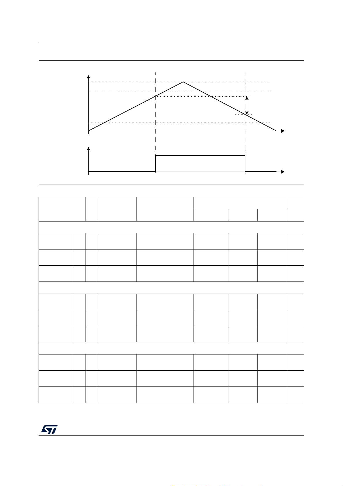
4.8.2 I/O output DC characteristics
Figure 4 provides description of output DC electrical characteristics.
Figure 4. I/O output DC electrical characteristics definition
DD_HV
.
Note: 10%/90% is the default condition for any parameter if not explicitly mentioned differently.
The following tables provide DC characteristics for bidirectional pads:
• Table 13 provides output driver characteristics for I/O pads when in WEAK/SLOW
configuration.
• Table 14 provides output driver characteristics for I/O pads when in MEDIUM
configuration.
• Table 15 provides output driver characteristics for I/O pads when in STRONG/FAST
configuration.
• Table 16 provides output driver characteristics for I/O pads when in VERY
STRONG/VERY FAST configuration.
DS11620 Rev 7 29/153
36
Electrical characteristics SPC584Cx, SPC58ECx
Table 13. WEAK/SLOW I/O output characteristics
Symbol C Parameter Conditions
=0.5mA
I
ol
VDD=5.0V ± 10%
=3.3V ± 10%
V
DD
Ioh=0.5mA
=5.0V ± 10%
V
DD
=3.3V ± 10%
V
DD
V
= 5.0 V ± 10% 380 — 1040
DD
= 3.3 V ± 10% 250 — 700
V
DD
V
V
R
ol_W
oh_W
_W
CC D
CC D
CC P
Output low
voltage for Weak
type PADs
Output high
voltage for Weak
type PADs
Output
impedance for
Weak type PADs
CL = 25 pF
=5.0V ± 10%
V
DD
=3.3V ± 10%
V
DD
CL = 50 pF
V
=5.0V ± 10%
DD
=3.3V ± 10%
V
DD
F
max_W
CC T
Maximum output
frequency for
Weak type PADs
CL = 25 pF
t
TR_W
CC T
Transition time
output pin
weak
configuration,
10%-90%
= 5.0 V + 10%
V
DD
VDD= 3.3 V + 10%
CL = 50 pF
V
=5.0V ± 10%
DD
=3.3V ± 10%
V
DD
Difference
|t
SKEW_W
| CC T
between rise
and fall time,
90%-10%
Value
Unit
Min Typ Max
— — 0.1*V
0.9*V
DD
——V
DD
V
Ω
——2MHz
——1MHz
25 — 120 ns
50 — 240 ns
———25%
=5.0V ± 10%
I
DCMAX_W
CC D
Maximum DC
current
Table 14. MEDIUM I/O output characteristics
V
DD
VDD=3.3V ± 10%
Symbol C Parameter Conditions
V
V
ol_M
oh_M
CC D
CC D
Output low
voltage for
Medium type
PAD s
Output high
voltage for
Medium type
PAD s
=2.0mA
I
ol
VDD=5.0 V ± 10 %
=3.3 V ± 10 %
V
DD
=2.0 mA
I
oh
VDD=5.0V ± 10%
=3.3V ± 10%
V
DD
30/153 DS11620 Rev 7
——0.5mA
Value
Unit
Min Typ Max
— — 0.1*V
0.9*V
DD
——V
DD
V

SPC584Cx, SPC58ECx Electrical characteristics
Table 14. MEDIUM I/O output characteristics (continued)
Value
Symbol C Parameter Conditions
Min Typ Max
Unit
R
_M
F
max_M
t
TR_M
|t
SKEW_M
I
DCMAX_M
CC P
CC T
CC T
| CC T
CC D
Output
impedance for
Medium type
PAD s
Maximum output
frequency for
Medium type
PAD s
Transition time
output pin
MEDIUM
configuration,
10%-90%
Difference
between rise
and fall time,
90%-10%
Maximum DC
current
= 5.0 V ± 10% 90 — 260
V
DD
VDD= 3.3 V ± 10% 60 — 170
CL = 25 pF
=5.0V ± 10%
V
DD
=3.3V ± 10%
V
DD
——12MHz
CL = 50 pF
V
=5.0V ± 10%
DD
=3.3V ± 10%
V
DD
——6MHz
CL = 25 pF
=5.0V ± 10%
V
DD
=3.3V ± 10%
V
DD
8 — 30 ns
CL = 50 pF
V
=5.0V ± 10%
DD
12 — 60 ns
VDD=3.3V ± 10%
———25%
VDD=5.0V ± 10%
=3.3V ± 10%
V
DD
——2mA
Ω
Table 15. STRONG/FAST I/O output characteristics
Symbol C Parameter Conditions
V
ol_S
CC D
Output low
voltage for
Strong type
PAD s
V
DD
VDD=3 .3 V ± 10%
Output high
V
V
oh_S
CC D
voltage for
Strong type
PAD s
Output
R
_S
CC P
impedance for
Strong type
PAD s
DD
VDD=3.3V ± 10%
V
DD
V
DD
Value
Unit
Min Typ Max
=8.0mA
I
ol
=5.0V ± 10%
I
=5.5mA
ol
=8.0mA
I
oh
=5.0V ± 10%
Ioh=5.5mA
— — 0.1*V
— — 0.15*V
0.9*V
0.85*V
——V
DD
——V
DD
DD
DD
V
V
= 5.0 V ± 10% 20 — 65
Ω
= 3.3 V ± 10% 28 — 90
DS11620 Rev 7 31/153
36

Electrical characteristics SPC584Cx, SPC58ECx
Table 15. STRONG/FAST I/O output characteristics (continued)
Value
Symbol C Parameter Conditions
Min Typ Max
Unit
F
max_S
t
TR_S
I
DCMAX_S
|t
SKEW_S
CC T
CC T
CC D
| CC T
Maximum output
frequency for
Strong type
PAD s
Transition time
output pin
STRONG
configuration,
10%-90%
Maximum DC
current
Difference
between rise
and fall time,
90%-10%
CL = 25 pF
=5.0 V ± 10%
V
DD
CL = 50 pF
=5.0 V ± 10%
V
DD
CL = 25 pF
=3.3V ± 10%
V
DD
CL = 50 pF
=3.3V ± 10%
V
DD
CL = 25 pF
=5.0V ± 10%
V
DD
CL = 50 pF
V
=5.0V ± 10%
DD
CL = 25 pF
V
=3.3V ± 10%
DD
CL = 50 pF
V
=3.3V ± 10%
DD
——50MHz
——25MHz
——25MHz
— — 12.5 MHz
3—10
5—16
1.5 — 15
2.5 — 26
VDD= 5 V ± 10% — — 8 mA
=3.3V ± 10% — — 5.5
V
DD
———25
ns
%
Table 16. VERY STRONG/VERY FAST I/O output characteristics
Symbol C Parameter Conditions
=9.0mA
I
ol
VDD=5.0 V ± 10%
Iol=9.0mA
=3.3 V ± 10%
V
DD
=9.0mA
I
oh
=5.0V ± 10%
V
DD
Ioh=9.0mA
=3.3V ± 10%
V
DD
= 5.0 V ± 10% 20 — 60
V
DD
= 3.3 V ± 10% 18 — 50
V
DD
V
V
ol_V
oh_V
R
_V
CC D
CC D
CC P
Output low
voltage for Very
Strong type
PAD s
Output high
voltage for Very
Strong type
PAD s
Output
impedance for
Very Strong type
PAD s
32/153 DS11620 Rev 7
Value
Min Typ Max
— — 0.1*V
— — 0.15*V
0.9*V
0.85*V
DD
DD
——V
——V
DD
DD
Unit
V
V
Ω

SPC584Cx, SPC58ECx Electrical characteristics
Table 16. VERY STRONG/VERY FAST I/O output characteristics (continued)
Value
Symbol C Parameter Conditions
Min Typ Max
Unit
F
max_V
t
TR_V
t
TR20-80_V
t
TRTTL_V
CC T
CC T
CC T
CC T
Maximum output
frequency for
Very Strong type
PAD s
10–90%
threshold
transition time
output pin VERY
STRONG
configuration
20–80%
threshold
transition time
output pin VERY
STRONG
configuration
(Flexray
Standard)
TTL threshold
transition time
for output pin in
VERY STRONG
configuration
(Ethernet
standard)
CL = 25 pF
=5.0V ± 10%
V
DD
CL = 50 pF
= 5.0 V ± 10%
V
DD
CL = 25 pF
=3.3V ± 10%
V
DD
CL = 50 pF
=3.3V ± 10%
V
DD
CL = 25 pF
=5.0V ± 10%
V
DD
CL = 50 pF
=5.0V ± 10%
V
DD
CL = 25 pF
V
=3.3V ± 10%
DD
CL = 50 pF
V
=3.3V ± 10%
DD
CL = 25 pF
=5.0V ± 10%
V
DD
CL = 15 pF
=3.3V ± 10%
V
DD
CL = 25 pF
=3.3V ± 10%
V
DD
——50MHz
——25MHz
——50MHz
——25MHz
1—6
3—12
ns
1.5 — 6
3—11
0.8 — 4.5
ns
1—4.5
0.88 — 5 ns
Σt
TR20-80_V
|t
SKEW_V
I
DCMAX_V
CC T
| CC T
CC D
Sum of
transition time
20–80% output
pin VERY
STRONG
configuration
Difference
between rise
and fall delay
Maximum DC
current
CL = 25 pF
=5.0V ± 10%
V
DD
CL = 15 pF
VDD=3.3V ± 10%
CL = 25 pF
VDD= 5.0 V ± 10%
= 5.0 V±10%
V
DD
V
=3.3V ± 10%
DD
——9
——9
0—1.2ns
——9mA
DS11620 Rev 7 33/153
ns
36

Electrical characteristics SPC584Cx, SPC58ECx
4.8.3 I/O pad current specifications
The I/O pads are distributed across the I/O supply segment. Each I/O supply segment is
associated to a V
DD/VSS
attached to the IO_Definition document.
Table 17 provides I/O consumption figures.
In order to ensure device reliability, the average current of the I/O on a single segment
should remain below the I
In order to ensure device functionality, the sum of the dynamic and static current of the I/O
on a single segment should remain below the I
Pad mapping on each segment can be optimized using the pad usage information provided
on the I/O Signal Description table.
Symbol C Parameter Conditions
supply pair as described in the device pinout Microsoft Excel file
RMSSEG
maximum value.
DYNSEG
maximum value.
Table 17. I/O consumption
(1)
Val ue
Unit
Min Typ Max
I
RMSSEG
I
RMS_W
I
RMS_M
I
RMS_S
SR D
CC D
CC D
CC D
Average consumption
Sum of all the DC I/O current
within a supply segment
RMS I/O current for WEAK
configuration
RMS I/O current for MEDIUM
configuration
RMS I/O current for STRONG
configuration
(2)
———80mA
= 25 pF, 2 MHz,
C
L
=5.0V ± 10%
V
DD
= 50 pF, 1 MHz,
C
L
VDD=5.0V ± 10%
C
= 25 pF, 2 MHz,
L
VDD=3.3V ± 10%
= 25 pF, 1 MHz,
C
L
= 3.3 V ± 10%
V
DD
C
= 25 pF, 12 MHz,
L
= 5.0 V ± 10%
V
DD
C
= 50 pF, 6 MHz,
L
V
= 5.0 V ± 10%
DD
= 25 pF, 12 MHz,
C
L
= 3.3 V ± 10%
V
DD
= 25 pF, 6 MHz,
C
L
VDD= 3.3 V ± 10%
C
= 25 pF, 50 MHz,
L
VDD= 5.0 V ± 10%
= 50 pF, 25 MHz,
C
L
= 5.0 V ± 10%
V
DD
= 25 pF, 25 MHz,
C
L
VDD= 3.3 V ± 10%
——1.1
——1.1
mA
——1.0
——1.0
——5.5
——5.5
mA
——4.2
——4.2
——21
——21
mA
——10
C
L
V
34/153 DS11620 Rev 7
= 25 pF, 12.5 MHz,
= 3.3 V ± 10%
DD
——10

SPC584Cx, SPC58ECx Electrical characteristics
Table 17. I/O consumption (continued)
(1)
Val ue
Symbol C Parameter Conditions
= 25 pF, 50 MHz,
C
L
= 5.0 V ± 10%
V
DD
= 50 pF, 25 MHz,
C
L
I
RMS_V
CC D
RMS I/O current for VERY
STRONG configuration
VDD= 5.0 V ± 10%
C
= 25 pF, 50 MHz,
L
VDD= 3.3 V ± 10%
= 25 pF, 25 MHz,
C
L
= 3.3 V ± 10%
V
DD
Dynamic consumption
(3)
Min Typ Max
——23
——23
——16
——16
Unit
mA
I
DYN_SEG
I
DYN_W
I
DYN_M
I
DYN_S
SR D
CC D
CC D
CC D
Sum of all the dynamic and DC
I/O current within a supply
segment
Dynamic I/O current for WEAK
configuration
Dynamic I/O current for
MEDIUM configuration
Dynamic I/O current for
STRONG configuration
VDD= 5.0 V ± 10% — — 195
= 3.3 V ± 10% — — 150
V
DD
=25pF, VDD=5.0V ±
C
L
10%
=50pF, VDD=5.0V ±
C
L
10%
C
=25pF, VDD=3.3V ±
L
10%
=50pF, VDD=3.3V ±
C
L
10%
CL=25pF, VDD=5.0V ±
10%
C
=50pF, VDD=5.0V ±
L
10%
=25pF, VDD=3.3V ±
C
L
10%
=50pF, VDD=3.3V ±
C
L
10%
C
=25pF, VDD=5.0V ±
L
10%
=50pF, VDD=5.0V ±
C
L
10%
=25pF, VDD=3.3V ±
C
L
10%
— — 16.7
— — 16.8
— — 12.9
— — 12.9
— — 18.2
— — 18.4
— — 14.3
— — 16.4
——57
— — 63.5
——31
mA
mA
mA
mA
C
=50pF, VDD=3.3V ±
L
10%
— — 33.5
DS11620 Rev 7 35/153
36

Electrical characteristics SPC584Cx, SPC58ECx
Table 17. I/O consumption (continued)
(1)
Val ue
Symbol C Parameter Conditions
Min Typ Max
=25pF, VDD=5.0V ±
C
L
10%
=50pF, VDD=5.0V ±
C
I
DYN_V
CC D
Dynamic I/O current for VERY
STRONG configuration
L
C
L
10%
=25pF, VDD=3.3V ±
10%
=50pF, VDD=3.3V ±
C
L
10%
1. I/O current consumption specifications for the 4.5 V ≤ V
VSIO[VSIO_xx] = 0 for 3.0 V
2. Average consumption in one pad toggling cycle.
3. Stated maximum values represent peak consumption that lasts only a few ns during I/O transition. When possible (timed
output) it is recommended to delay transition between pads by few cycles to reduce noise and consumption.
≤
V
DD_HV_IO
≤ 3.6 V.
DD_HV_IO
≤ 5.5 V range are valid for VSIO_[VSIO_xx] = 1, and
——62
——70
——52
——55
Unit
mA
36/153 DS11620 Rev 7

SPC584Cx, SPC58ECx Electrical characteristics
V
IL
V
DD
PORST
V
IH
device start-up phase
V
DD_POR
PORST driven low by
device reset
forced by external circuitry
PORST
undriven
device reset by
internal power-on reset
internal power-on reset
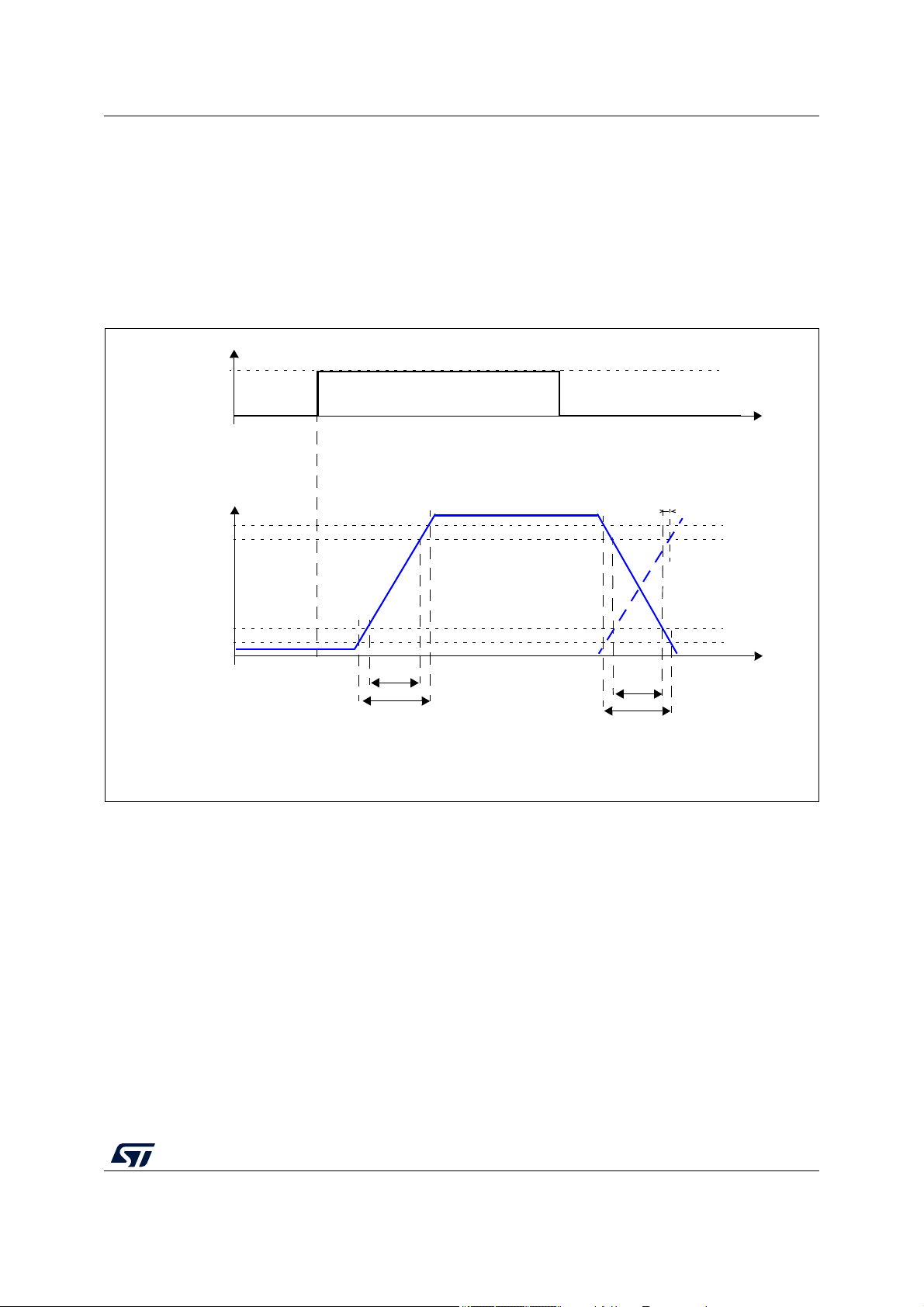
4.9 Reset pad (PORST) electrical characteristics
The device implements dedicated bidirectional reset pins as below specified. PORST pin
does not require active control. It is possible to implement an external pull-up to ensure
correct reset exit sequence. Recommended value is 4.7 KΩ.
Figure 5. Startup Reset requirements
Figure 6 describes device behavior depending on supply signal on PORST:
1. PORST
low pulse has too low amplitude: it is filtered by input buffer hysteresis. Device
remains in current state.
2. PORST
low pulse has too short duration: it is filtered by low pass filter. Device remains
in current state.
3. PORST
a) PORST
low pulse is generating a reset:
low but initially filtered during at least WFRST. Device remains initially in
current state.
b) PORST
potentially filtered until WNFRST. Device state is unknown. It may either
be reset or remains in current state depending on extra condition (temperature,
voltage, device).
c) PORST
asserted for longer than WNFRST. Device is under reset.
DS11620 Rev 7 37/153
39

Electrical characteristics SPC584Cx, SPC58ECx
V
IL
V
IH
V
DD
filtered by
hysteresis
filtered by
lowpass filter
W
FRST
W
NFRST
filtered by
lowpass filter
W
FRST
unknown reset
state
device under hardware reset
internal
reset
1 2 3a 3b 3c
V
HYS
V
PORST
Figure 6. Noise filtering on reset signal
Symbol C Parameter Conditions
V
IHRES
V
ILRES
V
HYSRES
V
DD_POR
SR P Input high level
SR P Input low level
CC C Input hysteresis
CC D Minimum supply
Table 18. Reset PAD electrical characteristics
V
TTL
TTL
TTL
for strong pull-
down activation
DD_HV
V
DD_HV
V
DD_HV
V
DD_HV
V
DD_HV
V
DD_HV
V
DD_HV
V
DD_HV
Value
Unit
Min Typ Max
=5.0V ± 10%
=3.3V ± 10%
2—V
DD_HV_IO
+0.3
V
= 5.0 V ± 10% -0.3 — 0.8 V
= 3.3 V ± 10% -0.3 — 0.6
=5.0V ± 10% 0.3 — — V
=3.3V ± 10% 0.2 — —
= 5.0 V ± 10% — — 1.6 V
= 3.3 V ± 10% — — 1.05
38/153 DS11620 Rev 7

SPC584Cx, SPC58ECx Electrical characteristics
Table 18. Reset PAD electrical characteristics (continued)
Value
Symbol C Parameter Conditions
Min Typ Max
Unit
I
OL_R
I
WPU
I
WPD
CC P Strong pull-down
current
(1)
CC P Weak pull-up
current absolute
PV
value
PV
PV
CC P Weak pull-down
current absolute
value
PV
PV
PV
V
V
=5.0V ± 10% 12 — — mA
DD_HV
=3.3V ± 10% 8 — —
DD_HV
VIN=1.1V
V
V
V
V
DD_HV
IN
DD_HV
IN
V
DD_HV_IO
DD_HV
=0.69 * V
IN
DD_HV
=5.0V ± 10%
=3.3V ± 10%
=5.0V ± 10%
=3.3V ± 10%
VIN= 0.69 *
V
DD_HV_IO
V
V
V
V
=5.0V ± 10%
DD_HV
IN
V
DD_HV_IO
=3.3V ± 10%
DD_HV
IN
=5.0V ± 10%
DD_HV
IN
DD_HVDD_HV
(2)
=1.1V
= 0.69 *
(3)
DD_HV_IO
(2)
= 0.69 *
(2)
=0.9V
=0.9V
=3.3V
— — 130 μA
——70
15 — —
15 — —
— — 130 μA
——80
15 — —
15 — —
± 10%
W
FRST
W
NFRST
1. I
applies to PORST: Strong Pull-down is active on PHASE0 for PORST. Refer to the device pinout IO definition excel file
ol_r
for details regarding pin usage.
2. Maximum current when forcing a change in the pin level opposite to the pull configuration.
3. Minimum current when keeping the same pin level state than the pull configuration.
CC P Input filtered
PV
pulse
CC P Input not filtered
PV
pulse
V
DD_HV
DD_HV
V
DD_HV
DD_HV
= 5.0 V ± 10% — — 500 ns
= 3.3 V ± 10% — — 600
=5.0V ± 10% 2000 — — ns
=3.3V ± 10% 3000 — —
PAD POWER-UP State RESET state DEFAULT state
Table 19. Reset Pad state during power-up and reset
(1)
STANDBY state
PORST Strong pull-down Weak pull-down Weak pull-down Weak pull-up
1. Before SW Configuration. Please refer to the Device Reference Manual, Reset Generation Module (MC_RGM) Functional
Description chapter for the details of the power-up phases.
DS11620 Rev 7 39/153
39

Electrical characteristics SPC584Cx, SPC58ECx
PLL0
PLL1
IRCOSC
XOSC
PLL1_PHI
PLL0_PHI1
PLL0_PHI
4.10 PLLs
Two phase-locked loop (PLL) modules are implemented to generate system and auxiliary
clocks on the device.
Figure 7 depicts the integration of the two PLLs. Refer to device Reference Manual for more
detailed schematic.
Figure 7. PLLs integration
4.10.1 PLL0
Symbol C Parameter Conditions
f
PLL0IN
Δ
PLL0IN
f
INFIN
f
PLL0VCO
f
PLL0PHI0
f
PLL0PHI1
t
PLL0LOCK
|Δ
PLL0PHI0SPJ
(3)
|
Table 20. PLL0 electrical characteristics
Val ue
Unit
Min Typ Max
SR — PLL0 input clock
SR —
PLL0 input clock duty
(1)
cycle
PLL0 PFD (Phase
SR —
Frequency Detector) input
clock frequency
CC P PLL0 VCO frequency — 600 — 1400 MHz
CC D PLL0 output frequency — 4.762 — 400 MHz
CC D PLL0 output clock PHI1 — 20 — 175
CC P PLL0 lock time — — — 100 µs
PLL0_PHI0 single period
CC T
jitter
fPLL0IN = 20 MHz
(resonator)
(1)
f
PLL0PHI0
6-sigma pk-pk
—8—44MHz
—40—60%
—8—20MHz
(2)
MHz
= 400 MHz,
— — 200 ps
40/153 DS11620 Rev 7

SPC584Cx, SPC58ECx Electrical characteristics
Table 20. PLL0 electrical characteristics (continued)
Val ue
Symbol C Parameter Conditions
Min Typ Max
PLL0_PHI1 single period
|Δ
PLL0PHI1SPJ
|
(3)
CC D
jitter
fPLL0IN = 20 MHz
f
PLL0PHI1
= 40 MHz,
6-sigma pk-pk
— — 300
(resonator)
10 periods
accumulated jitter
(80 MHz equivalent
— — ±250 ps
frequency), 6-sigma
pk-pk
Δ
PLL0LTJ
(3)
CC D
PLL0 output long term
(4)
jitter
f
= 20 MHz
PLL0IN
(resonator), VCO
frequency = 800 MHz
16 periods
accumulated jitter
(50 MHz equivalent
frequency), 6-sigma
pk-pk
— — ±300 ps
long term jitter
(< 1 MHz equivalent
frequency), 6-sigma
— — ±500 ps
pk-pk)
I
PLL0
1. PLL0IN clock retrieved directly from either internal RCOSC or external FXOSC clock. Input characteristics are granted
when using internal RCOSC or external oscillator is used in functional mode.
2. If the PLL0_PHI1 is used as an input for PLL1, then the PLL0_PHI1 frequency shall obey the maximum input frequency
limit set for PLL1 (87.5 MHz, according to Table 21).
3. Jitter values reported in this table refer to the internal jitter, and do not include the contribution of the divider and the path to
the output CLKOUT pin.
4. V
noise due to application in the range V
DD_LV
filtered.
CC D PLL0 consumption FINE LOCK state — — 6 mA
= 1.20 V±5%, with frequency below PLL bandwidth (40 kHz) will be
DD_LV
(4)
Unit
ps
DS11620 Rev 7 41/153
42

Electrical characteristics SPC584Cx, SPC58ECx
4.10.2 PLL1
PLL1 is a frequency modulated PLL with Spread Spectrum Clock Generation (SSCG)
support.
Symbol C Parameter Conditions
f
PLL1IN
Δ
PLL1IN
f
INFIN
f
PLL1VCO
f
PLL1PHI0
t
PLL1LOCK
f
PLL1MOD
|δ
PLL1MOD
|Δ
PLL1PHI0SPJ
(4)
SR — PLL1 input clock
SR —
SR —
CC P PLL1 VCO frequency — 600 — 1400 MHz
CC D PLL1 output clock PHI0 — 4.762 — F
CC P PLL1 lock time — — — 50 µs
CC T
|CCT
|
CC T
Table 21. PLL1 electrical characteristics
(1)
PLL1 input clock duty
(1)
cycle
PLL1 PFD (Phase
Frequency Detector)
input clock frequency
PLL1 modulation
frequency
PLL1 modulation depth
(when enabled)
PLL1_PHI0 single period
peak to peak jitter
200 MHz, 6-sigma
— 37.5 — 87.5 MHz
—35—65%
— 37.5 87.5 MHz
— — — 250 kHz
Center spread
(3)
Down spread 0.5 — 4 %
f
PLL1PHI0
=
Value
Unit
Min Typ Max
(2)
SYS
MHz
0.25 — 2 %
——500
(5)
ps
I
PLL1
1. PLL1IN clock retrieved directly from either internal PLL0 or external FXOSC clock. Input characteristics are granted when
using internal PPL0 or external oscillator is used in functional mode.
2. Refer to Section 4.3: Operating conditions for the maximum operating frequency.
3. The device maximum operating frequency F
the FSYS must be below the maximum by MD (Modulation Depth Percentage), such that FSYS(max)=FSYS(1+MD%).
Refer to the Reference Manual for the PLL programming details.
4. Jitter values reported in this table refer to the internal jitter, and do not include the contribution of the divider and the path to
the output CLKOUT pin.
5. 1.25 V±5%, application noise below 40 kHz at V
CC D PLL1 consumption FINE LOCK state — — 5 mA
(max) includes the frequency modulation. If center modulation is selected,
SYS
pin - no frequency modulation.
DD_LV
42/153 DS11620 Rev 7

SPC584Cx, SPC58ECx Electrical characteristics
4.11 Oscillators
4.11.1 Crystal oscillator 40 MHz
Table 22. External 40 MHz oscillator electrical specifications
Symbol C Parameter Conditions
f
XTAL
V
IHEXT
t
cst
t
rec
CC D Crystal Frequency
Range
(1)
CC T Crystal start-up time
CC D Crystal recovery time
CC D EXTAL input high
voltage
(6)
(External
(3),(4)
(5)
TJ= 150 °C — 5 ms
V
= 0.29 * V
REF
Reference)
V
ILEXT
CC D EXTAL input low
voltage
(6)
(External
V
REF
= 0.29 * V
Reference)
C
S_EXTAL
C
S_XTAL
CC D Total on-chip stray
capacitance on EXTAL
pin
(7)
CC D Total on-chip stray
capacitance on XTAL
pin
(7)
Value
Unit
Min Max
—4
(2)
8MHz
>8 20
>20 40
——0.5ms
DD_HV_OSC
REF
+
—V
V
0.75
DD_HV_OSC
—V
REF
-
V
0.75
—37pF
—37pF
V
EXTAL
g
m
CC P Oscillator
Transconductance
Df
f
= 4 − 8MHz
XTAL
freq_sel[2:0] = 000
= 5 - 10 MHz
XTAL
3.9 13.6 mA/V
517.5
freq_sel[2:0] = 001
Df
= 10 − 15 MHz
XTAL
8.6 29.3
freq_sel[2:0] = 010
Pf
= 15 - 20 MHz
XTAL
14.4 48
freq_sel[2:0] = 011
Df
= 20 - 25 MHz
XTAL
21.2 69
freq_sel[2:0] = 100
Df
= 25 − 30 MHz
XTAL
27 86
freq_sel[2:0] = 101
Df
= 30 - 35 MHz
XTAL
33.5 115
freq_sel[2:0] = 110
Pf
= 35 - 40 MHz
XTAL
33.5 115
freq_sel[2:0] = 111
CC D Oscillation Amplitude on
the EXTAL pin after
startup
(8)
TJ = –40 °C to 150 °C 0.5 1.8 V
DS11620 Rev 7 43/153
46

Electrical characteristics SPC584Cx, SPC58ECx
Table 22. External 40 MHz oscillator electrical specifications (continued)
Value
Symbol C Parameter Conditions
Min Max
Unit
V
HYS
I
XTAL
1. The range is selectable by UTEST miscellaneous DCF client XOSC_FREQ_SEL.
2. The XTAL frequency, if used to feed the PPL0 (or PLL1), shall obey the minimum input frequency limit set for PLL0 (or
PLL1).
3. This value is determined by the crystal manufacturer and board design, and it can potentially be higher than the maximum
provided.
4. Proper PC board layout procedures must be followed to achieve specifications.
5. Crystal recovery time is the time for the oscillator to settle to the correct frequency after adjustment of the integrated load
capacitor value.
6. Applies to an external clock input and not to crystal mode.
7. See crystal manufacturer’s specification for recommended load capacitor (C
external load capacitors when operating from 8 MHz to 16 MHz. Account for on-chip stray capacitance (C
and PCB capacitance when selecting a load capacitor value. When operating at 20 MHz/40 MHz, the integrated load
capacitor value is selected via S/W to match the crystal manufacturer’s specification, while accounting for on-chip and PCB
capacitance.
8. Amplitude on the EXTAL pin after startup is determined by the ALC block, that is the Automatic Level Control Circuit. The
function of the ALC is to provide high drive current during oscillator startup, but reduce current after oscillation in order to
reduce power, distortion, and RFI, and to avoid over driving the crystal. The operating point of the ALC is dependent on the
crystal value and loading conditions.
9. I
is the oscillator bias current out of the XTAL pin with both EXTAL and XTAL pins grounded. This is the maximum
XTAL
current during startup of the oscillator.
CC D Comparator Hysteresis TJ= –40 °C to 150 °C 0.1 1.0 V
CC D XTAL current
(8),(9)
TJ = –40 °C to 150 °C — 14 mA
) values. The external oscillator requires
L
S_EXTAL/CS_XTAL
4.11.2 Crystal Oscillator 32 kHz
Table 23. 32 kHz External Slow Oscillator electrical specifications
)
Symbol C Parameter Conditions
f
sxosc
SR T Slow external
crystal oscillator
frequency
g
msxosc
CC P Slow external
crystal oscillator
transconductance
V
sxosc
CC T Oscillation
Amplitude
I
sxoosc
CC D Oscillator
consumption
T
sxosc
CC T Start up time — — — 2 s
Value
Unit
Min Typ Max
— — 32768 — Hz
—9.5—32µA/V
—0.5—1.7V
———9µA
44/153 DS11620 Rev 7

SPC584Cx, SPC58ECx Electrical characteristics
4.11.3 RC oscillator 16 MHz
Table 24. Internal RC oscillator electrical specifications
Value
Symbol C Parameter Conditions
Min Typ Max
f
Ta rg e t
δf
var_noT
CC D IRC target frequency — — 16 — MHz
CC P IRC frequency variation
T < 150 °C –5 — 5 %
without temperature
compensation
δf
var_T
CC T IRC frequency variation
T < 150 °C –3 — 3 %
with temperature
compensation
δf
var_SW
T
start_noT
T IRC software trimming
accuracy
CC T Startup time to reach within
f
var_noT
Trimming
temperature
Factory
trimming
–0.5 +0.3 0.5 %
—— 5 µs
already
applied
T
start_T
CC T Startup time to reach within
f
var_T
Factory
trimming
——120µs
already
applied
I
FIRC
1. The actual consumption difference can be higher due to additional consumption of core logic clocked by RCOSC16M.
CC T Current consumption on HV
power supply
(1)
After T
start_T
— — 1200 µA
Unit
DS11620 Rev 7 45/153
46

Electrical characteristics SPC584Cx, SPC58ECx
4.11.4 Low power RC oscillator
Table 25. 1024 kHz internal RC oscillator electrical characteristics
Val ue
Symbol C Parameter Conditions
Min Typ Max
Unit
F
δf
δf
T
sirc
var_T
var_V
I
sirc
sirc
CC T Slow Internal
RC oscillator
frequency
CC P Frequency
variation across
temperature
CC P Frequency
variation across
voltage
CC T Slow Internal
RC oscillator
current
CC T Start up time,
after switching
ON the internal
regulator.
— — 1024 — kHz
–40 °C < T <
–9 — +9 %
150 °C
–40 °C < T <
–5 — +5 %
150 °C
T = 55 °C — — 6 µA
———12µS
46/153 DS11620 Rev 7

SPC584Cx, SPC58ECx Electrical characteristics
R
SW1
C
P2
C
S
V
DD
Sampling
INTERNAL CIRCUIT SCHEME
R
SW1
: Channel Selection Switch Impedance
R
AD
: Sampling Switch Impedance
C
P
: Pin Capacitance (two contributions, CP1 and CP2)
C
S
: Sampling Capacitance
R
CMSW
: Common mode switch
R
CMRL
: Common mode resistive ladder
V
CM
: Common mode voltage (~0.5 VDD)
C
EXT
: External capacitance
C
P1
R
AD
Channel
Selection
Common mode
switch
Common mode
resistive ladder
The above scheme can be used as approximation circuitry for external filtering definition.
V
CM
R
CMSW
R
CMRL
C
EXT
V
SS_HV_ADR
4.12 ADC system
4.12.1 ADC input description
Figure 8 shows the input equivalent circuit for SARn and SARB channels.
Figure 8. Input equivalent circuit (Fast SARn and SARB channels)
All specifications in the following table are valid for the full input voltage range for the analog
inputs.
Symbol C Parameter Conditions
R
20KΩ
I
LKG
I
INJ1
C
HV_ADC
C
P1
CC D
CC —
SR —
SR D V
CC D Pad capacitance
Table 26. ADC pin specification
Internal voltage reference source
impedance.
Input leakage current, two ADC
channels on input-only pin.
Injection current on analog input
preserving functionality at full or
degraded performances.
DD_HV_ADV
external capacitance.
DS11620 Rev 7 47/153
Value
Unit
Min Max
—1630KΩ
See IO chapter Table 11: I/O input electrical
characteristics, parameter I
See Operating Conditions chapter Table 5:
Operating conditions, I
See Power Management chapter Table 34: External
INJ1
components integration, C
See IO chapter Table 11: I/O input electrical
characteristics, parameter C
.
LKG
parameter.
parameter.
ADC
.
P1
55

Electrical characteristics SPC584Cx, SPC58ECx
Table 26. ADC pin specification (continued)
Value
Symbol C Parameter Conditions
Min Max
SARB channels — 2
Unit
C
P2
CC D Internal routing capacitance
pFSARn 10bit channels — 0.5
SARn 12bit channels — 1
SARn 12bit — 5
C
S
CC D SAR ADC sampling capacitance
SARn 10bit — 2
pF
SARB channels 0 1.8
R
SWn
CC D Analog switches resistance
kΩSARn 10bit channels 0 0.8
SARn 12bit channels 0 1.8
SARn 12bit — 0.8
SARn 10bit — 3.2
Sum of the two
resistances
V
DD_HV_IO
V
DD_HV_IO
= 5.0 V ± 10% — 300 W
= 3.3 V ± 10% — 500 W
kΩ
kΩ
—9
R
R
R
SAFEPD
A
R
AD
CMSW
CMRL
BGAP
CC D
ADC input analog switches
resistance
CC D Common mode switch resistance
CC D Common mode resistive ladder kΩ
(1)
CC D
Discharge resistance for ADC
input-only pins (strong pull-down
for safety)
CC D ADC digital bandgap accuracy -1.5 +1.5 %
To preserve the accuracy of the ADC, it is necessary
that analog input pins have low AC impedance.
Placing a capacitor with good high frequency
C
EXT
SR —
External capacitance at the pad
input pin
characteristics at the input pin of the device can be
effective: the capacitor should be as large as
possible. This capacitor contributes to attenuating
the noise present on the input pin. The impedance
relative to the signal source can limit the ADC’s
sample rate.
1. It enables discharge of up to 100 nF from 5 V every 300 ms. Refer to the device pinout Microsoft Excel file attached to the
IO_Definition document for the pads supporting it.
4.12.2 SAR ADC 12-bit electrical specification
The SARn ADCs are 12-bit Successive Approximation Register analog-to-digital converters
with full capacitive DAC. The SARn architecture allows input channel multiplexing.
Note: The functional operating conditions are given in the DC electrical specifications. Absolute
maximum ratings are stress ratings only, and functional operation at the maxima is not
guaranteed. Stress beyond the listed maximum may affect device reliability or cause
permanent damage to the device.
48/153 DS11620 Rev 7

SPC584Cx, SPC58ECx Electrical characteristics
Table 27. SARn ADC electrical specification
Symbol C Parameter Conditions
f
ADCK
t
ADCINIT
t
ADCBIASINIT
P
SR
Clock frequency
T High frequency mode >13.33 16.0
SR — ADC initialization time — 1.5 — µs
SR —
ADC BIAS
initialization time
Standard frequency mode 7.5 13.33
Fast SAR 1/f
t
ADCPRECH
ΔV
PRECH
SR T ADC decharge time
SR D
Decharge voltage
precision
Slow SAR (SARDAC_B) 2/f
TJ<150°C 0 0.25 V
Internal voltage
R
20KΩ
CC D
reference source
impedance
Applies to all internal
reference points
ΔV
INTREF
CC P
Internal reference
voltage precision
(V
SS_HV_ADR
1/3 * V
DD_HV_ADR
2/3 * V
DD_HV_ADR
V
DD_HV_ADR
Value
Unit
Min Max
MHz
—5—µs
ADCK
ADCK
—
µs
—
—1630KΩ
,
,
−0.20 0.20 V
,
)
DS11620 Rev 7 49/153
55

Electrical characteristics SPC584Cx, SPC58ECx
Table 27. SARn ADC electrical specification (continued)
Value
Symbol C Parameter Conditions
Min Max
Unit
t
ADCSAMPLE
t
ADCEVAL
I
ADCREFH
I
ADCREFL
I
ADV_S
(5),(6)
(6)
(6)
P
Fast SAR – 12-bit
configuration
Fast SAR – 10-bit
configuration mode 1
(2)
(Standard frequency mode
6/f
6/f
ADCK
ADCK
only)
Fast SAR – 10-bit
configuration mode 2
(Standard frequency mode
(3)
5/f
ADCK
only)
Fast SAR – 10-bit
configuration mode 3
(4)
6/f
ADCK
(High frequency mode only)
SR
ADC sample time
D
Slow SAR (SARADC_B) –
12-bit configuration
(1)
Slow SAR (SARADC_B) –
10-bit configuration mode
(2)
1
12/f
12/f
ADCK
ADCK
(Standard frequency mode
only)
Slow SAR (SARADC_B) –
10-bit configuration mode
(3)
2
10/f
ADCK
(Standard frequency mode
only)
Slow SAR (SARADC_B) –
10-bit configuration mode
(4)
3
12/f
ADCK
(High frequency mode only)
Conversion of BIAS test
channels through 20 kΩ
40/f
ADCK
input.
P
SR
ADC evaluation time
D 10-bit configuration 10/f
CC T
ADC high reference
current
12-bit configuration 12/f
Run mode
(average across all codes)
ADCK
ADCK
—7
Power Down mode — 1
Run mode
V
CC D
CC
ADC low reference
current
P
V
DD_HV_ADV
supply current
D Power Down mode — 0.04
power
DD_HV_ADR_S
Power Down mode
V
DD_HV_ADR_S
Run mode — 4.0
≤ 5.5 V
≤ 5.5 V
—15
—1
—µs
—
µs
—
µA
µA
mA
50/153 DS11620 Rev 7

SPC584Cx, SPC58ECx Electrical characteristics
Table 27. SARn ADC electrical specification (continued)
Value
Symbol C Parameter Conditions
TJ<150°C,
TUE
T
P
Total unadjusted error
12
CC
in 12-bit
configuration
T
(7)
V
DD_HV_ADV
V
DD_HV_ADR_S
T
<150°C,
J
V
DD_HV_ADV
V
DD_HV_ADR_S
T
<150°C,
J
V
DD_HV_ADV
3V>V
>3V,
>3V,
>3V,
DD_HV_ADR_S
High frequency mode,
<150°C,
T
D
J
V
DD_HV_ADV
V
DD_HV_ADR_S
>3V,
Mode 1, TJ<150°C,
D
V
DD_HV_ADV
V
DD_HV_ADR_S
>3V
Mode 1, TJ<150°C,
TUE
D
Total unadjusted error
10
CC
in 10-bit
configuration
(7)
C
C
V
DD_HV_ADV
3V>V
DD_HV_ADR_S
Mode 2, T
V
DD_HV_ADV
V
DD_HV_ADR_S
Mode 3, T
V
DD_HV_ADV
V
DD_HV_ADR_S
J
J
>3V,
<150°C,
>3V
<150°C,
>3V
Min Max
–4 4
>3V
–6 6
>3V
–6 6
>2V
–12 12
>3V
–1.5 1.5
>3V
–2.0 2.0
>2V
–3.0 3.0
>3V
–4.0 4.0
>3V
Unit
LSB
(12b)
LSB
(10b)
DS11620 Rev 7 51/153
55

Electrical characteristics SPC584Cx, SPC58ECx
Table 27. SARn ADC electrical specification (continued)
Value
Symbol C Parameter Conditions
V
< V
IN
DD_HV_ADV
V
DD_HV_ADR
∈ [0:25 mV]
V
< V
IN
DD_HV_ADV
V
DD_HV_ADR
∈ [25:50 mV]
< V
V
IN
DD_HV_ADV
V
DD_HV_ADR
∈ [50:75 mV]
< V
V
IN
DD_HV_ADV
V
DD_HV_ADR
∈ [75:100 mV]
ΔTUE
TUE degradation due
to V
12
CC D
DD_HV_ADR
with respect to
V
DD_HV_ADV
offset
V
DD_HV_ADV
V
DD_HV_ADR
V
DD_HV_ADR
∈ [0:25 mV]
− V
DD_HV_ADV
− V
DD_HV_ADV
− V
DD_HV_ADV
− V
DD_HV_ADV
< V
IN
− V
DD_HV_ADV
Min Max
–1 1
–2 2
–4 4
–6 6
<
–2.5 2.5
Unit
LSB
(12b)
V
DD_HV_ADV
V
DD_HV_ADR
V
DD_HV_ADR
< V
IN
− V
DD_HV_ADV
<
–4 4
∈ [25:50 mV]
V
DD_HV_ADV
V
DD_HV_ADR
V
DD_HV_ADR
< V
IN
− V
DD_HV_ADV
<
–7 7
∈ [50:75 mV]
V
DD_HV_ADV
V
DD_HV_ADR
V
DD_HV_ADR
< V
IN
− V
DD_HV_ADV
<
–12 12
∈ [75:100 mV]
Standard frequency mode,
P
DNL
(8)
CC
Differential nonlinearity
T
1. Minimum ADC sample times are dependent on adequate charge transfer from the external driving circuit to the internal
sample capacitor. The time constant of the entire circuit must allow the sampling capacitor to charge within 1/2 LSB within
the sampling window. Refer to Figure 8 for models of the internal ADC circuit, and the values to use in external RC sizing
and calculating the sampling window duration.
2. Mode1: 6 sampling cycles + 10 conversion cycles at 13.33 MHz.
3. Mode2: 5 sampling cycles + 10 conversion cycles at 13.33 MHz.
4. Mode3: 6 sampling cycles + 10 conversion cycles at 16 MHz.
5. I
ADCREFH
by the transfer of charge between internal capacitances during the conversion.
6. Current parameter values are for a single ADC.
and I
ADCREFL
are independent from ADC clock frequency. It depends on conversion rate: consumption is driven
V
DD_HV_ADV
V
DD_HV_ADR_S
> 4 V
> 4 V
High frequency mode,
V
DD_HV_ADV
V
DD_HV_ADR_S
> 4 V
> 4 V
–1 2
–1 2
LSB
(12b)
52/153 DS11620 Rev 7

SPC584Cx, SPC58ECx Electrical characteristics
7. TUE is granted with injection current within the range defined in Table 26, for parameters classified as T and D.
8. DNL is granted with injection current within the range defined in Table 26, for parameters classified as T and D.
4.12.3 SAR ADC 10-bit electrical specification
The ADC comparators are 10-bit Successive Approximation Register analog-to-digital
converters with full capacitive DAC. The SARn architecture allows input channel
multiplexing.
Note: The functional operating conditions are given in the DC electrical specifications. Absolute
maximum ratings are stress ratings only, and functional operation at the maxima is not
guaranteed. Stress beyond the listed maximum may affect device reliability or cause
permanent damage to the device.
Symbol C Parameter Conditions
Table 28. ADC-Comparator electrical specification
Value
Unit
Min Max
f
ADCK
t
ADCINIT
t
ADCBIASINIT
t
ADCINITSBY
t
ADCPRECH
ΔV
PRECH
t
ADCSAMPLE
t
ADCEVAL
I
ADCREFH
(3),(4)
SR
P
Clock frequency
Standard frequency mode 7.5 13.33
MHz
T High frequency mode >13.33 16.0
SR — ADC initialization time — 1.5 — µs
SR —
SR —
SR T ADC precharge time
SR D
SR P ADC sample time
SR
CC T
ADC BIAS initialization
time
ADC initialization time
in standby
Standby Mode 8 — µs
—5—µs
Fast channel 1/f
Standard channel 2/f
Precharge voltage
precision
(1)
P
TJ< 150 °C 0 0.25 V
10-bit ADC mode, Fast
channel
10-bit ADC mode, Standard
channel
5/f
6/f
10-bit ADC mode 10/f
ADC evaluation time
D ADC comparator mode 2/f
Run mode
ADC high reference
current
(average across all codes)
Power Down mode — 1
ADCK
ADCK
ADCK
ADCK
ADCK
ADCK
—
—
(2)
—µs
—µs
—
—
—7
µs
µs
µA
ADC comparator mode — 19.5
I
ADCREFL
(5)
CC D
ADC low reference
current
Run mode
V
DD_HV_ADR_S
V
DD_HV_ADR_S
≤ 5.5 V
≤ 5.5 V
—15
—1
µAPower Down mode
ADC comparator mode — 20.5
DS11620 Rev 7 53/153
55

Electrical characteristics SPC584Cx, SPC58ECx
Table 28. ADC-Comparator electrical specification (continued)
Value
Symbol C Parameter Conditions
Min Max
Unit
I
ADV_S
TUE
10
(5)
P
V
CC
DD_HV_ADV
supply current
D Power Down mode — 0.04
power
Run mode — 4
TJ< 150 °C,
T
V
DD_HV_ADV
V
DD_HV_ADR_S
>3V,
>3V
–2 2
TJ< 150 °C,
–3 3
–3 3
CC
P
Total unadjusted error
in 10-bit configuration
T
V
DD_HV_ADV
V
DD_HV_ADR_S
(6)
T
J
V
DD_HV_ADV
3V>V
< 150 °C,
DD_HV_ADR_S
>3V,
>3V
>3V,
>2V
High frequency mode,
< 150 °C,
T
D
J
V
DD_HV_ADV
V
DD_HV_ADR_S
V
< V
IN
DD_HV_ADV
V
DD_HV_ADR
>3V,
>3V
− V
DD_HV_ADV
∈
–3 3
–1.0 1.0
[0:25 mV]
V
< V
IN
DD_HV_ADV
V
DD_HV_ADR
− V
DD_HV_ADV
∈
–2.0 2.0
[25:50 mV]
< V
V
IN
DD_HV_ADV
V
DD_HV_ADR
− V
DD_HV_ADV
∈
–3.5 3.5
[50:75 mV]
mA
LSB
(10b)
< V
V
IN
DD_HV_ADV
V
DD_HV_ADR
[75:100 mV]
ΔTUE
TUE degradation due
to V
10
CC D
DD_HV_ADR
with respect to
V
DD_HV_ADV
offset
V
DD_HV_ADV
V
DD_HV_ADR
V
DD_HV_ADR
[0:25 mV]
V
DD_HV_ADV
V
DD_HV_ADR
V
DD_HV_ADR
[25:50 mV]
V
DD_HV_ADV
V
DD_HV_ADR
V
DD_HV_ADR
[50:75 mV]
V
DD_HV_ADV
V
DD_HV_ADR
V
DD_HV_ADR
[75:100 mV]
54/153 DS11620 Rev 7
− V
DD_HV_ADV
< V
IN
− V
DD_HV_ADV
< V
IN
− V
DD_HV_ADV
< V
IN
− V
DD_HV_ADV
< V
IN
− V
DD_HV_ADV
–6.0 6.0
∈
<
–2.5 2.5
∈
LSB
(10b)
<
–4.0 4.0
∈
<
–7.0 7.0
∈
<
–12.0 12.0
∈

SPC584Cx, SPC58ECx Electrical characteristics
Table 28. ADC-Comparator electrical specification (continued)
Value
Symbol C Parameter Conditions
Min Max
Standard frequency mode,
P
DNL
(7)
CC
Differential non-linearity
std. mode
T
1. Minimum ADC sample times are dependent on adequate charge transfer from the external driving circuit to the internal
sample capacitor. The time constant of the entire circuit must allow the sampling capacitor to charge within 1/2 LSB within
the sampling window. Refer to Figure 8 for models of the internal ADC circuit, and the values to use in external RC sizing
and calculating the sampling window duration.
2. In case the ADC is used as Fast Comparator the sampling time is t
3. I
ADCREFH
by the transfer of charge between internal capacitances during the conversion.
4. Current parameter values are for a single ADC.
5. All channels of all SAR-ADC12bit and SAR-ADC10bit are impacted with same degradation, independently from the ADC
and the channel subject to current injection.
6. TUE is granted with injection current within the range defined in Table 26, for parameters classified as T and D.
7. DNL is granted with injection current within the range defined in Table 26, for parameters classified as T and D.
and I
ADCREFL
are independent from ADC clock frequency. It depends on conversion rate: consumption is driven
V
DD_HV_ADV
V
DD_HV_ADR_S
High frequency mode,
V
DD_HV_ADV
V
DD_HV_ADR_S
> 4 V
> 4 V
> 4 V
> 4 V
ADCSAMPLE
= 2/f
ADCK
.
–1 2
–1 2
Unit
LSB
(10b)
DS11620 Rev 7 55/153
55

Electrical characteristics SPC584Cx, SPC58ECx
4.13 Temperature Sensor
The following table describes the temperature sensor electrical characteristics.
Table 29. Temperature sensor electrical characteristics
Value
Symbol C Parameter Conditions
Min Typ Max
— CC — Temperature monitoring range — –40 — 150 °C
T
T
SENS
ACC
CC T Sensitivity — — 5.18 — mV/°C
CC P Accuracy TJ < 150 °C–3—3°C
Unit
56/153 DS11620 Rev 7

SPC584Cx, SPC58ECx Electrical characteristics
Signal excursions above this level NOT allowed
Max. common mode input at RX
Signal excursions below this level NOT allowed
Min. common mode input at RX
Data Bit Period
Minimum Data Bit Time
Opening =
0.55 * T (LFAST)
Max Differential Voltage =
285 mV (LFAST)
Min Differential
Voltage =
100 mV (LFAST)
1743 mV
1600 mV
V
OS
= 1.2 V +/- 10%
TX common mode
V
ICOM
150 mV
0V
1743 mV
“No-Go”
T = 1 /F
DATA
|Δ
VOD
|
|Δ
VOD
|
ΔPER
EYE
ΔPER
EYE
PAD _N
PAD _P
4.14 LFAST pad electrical characteristics
The LFAST(LVDS Fast Asynchronous Serial Transmission) pad electrical characteristics
apply to high-speed debug serial interfaces on the device.
4.14.1 LFAST interface timing diagrams
Figure 9. LFAST LVDS timing definition
DS11620 Rev 7 57/153
62

Electrical characteristics SPC584Cx, SPC58ECx
Data Valid
pad_p/pad_n
lfast_pwr_down
Differential TX
Data Lines
H
L
t
PD2NM_TX
Differential TX
Data Lines
pad_p/pad_n
t
TR
t
TR
|ΔVOD(min)|
|ΔVOD(min)|
V
IH
V
IL
Figure 10. Power-down exit time
4.14.2 LFAST LVDS interface electrical characteristics
Symbol
t
STRT_BIAS
t
PD2NM_TX
58/153 DS11620 Rev 7
Figure 11. Rise/fall time
The following table contains the electrical characteristics for the LFAST interface.
Table 30. LVDS pad startup and receiver electrical characteristics
(1), (2)
C Parameter Conditions
Min Typ Max
(3),(4)
——0.54μs
——0.42.75μs
CC T
CC T
STARTUP
Bias current reference startup
Transmitter startup time (power
down to normal mode)
time
(5)
(6)
Value
Unit

SPC584Cx, SPC58ECx Electrical characteristics
Table 30. LVDS pad startup and receiver electrical characteristics (continued)
Value
Unit
Symbol
(1), (2)
C Parameter Conditions
Min Typ Max
t
SM2NM_TX
t
PD2NM_RX
t
PD2SM_RX
I
LVD S_B IAS
CC T
CC T
CC T
Transmitter startup time (sleep
mode to normal mode)
Receiver startup time (power
down to normal mode)
Receiver startup time (power
down to sleep mode)
(7)
(8)
(9)
CC D LVDS bias current consumption Tx or Rx enabled — — 0.95 mA
Not applicable to the
MSC/DSPI LVDS pad
— — 20 40 ns
Not applicable to the
MSC/DSPI LVDS pad
—0.40.6µs
—2050ns
TRANSMISSION LINE CHARACTERISTICS (PCB Track)
Transmission line characteristic
impedance
Transmission line differential
impedance
—47.55052.5Ω
— 95 100 105 Ω
Z
Z
0
DIFF
SR D
SR D
RECEIVER
V
ICOM
|ΔVI| SR T Differential input voltage
V
HYS
R
IN
SR T Common mode voltage —
(12)
—100——mV
CC T Input hysteresis — 25 — — mV
CC D Terminating resistance V
DD_HV_IO
=
5.0 V ± 10%
°C<T
V
DD_HV_IO
<150°C
J
=
-40
3.3 V ± 10%
°C<T
-40
C
IN
I
LVD S_R X
I
PIN_RX
1. The LVDS pad startup and receiver electrical characteristics in this table apply to both the LFAST & High-speed Debug
(HSD) LVDS pad.
2. All LVDS pad electrical characteristics are valid from -40 °C to 150 °C.
3. All startup times are defined after a 2 peripheral bridge clock delay from writing to the corresponding enable bit in the LVDS
control registers (LCR) of the LFAST and High-speed Debug modules. The value of the LCR bits for the LFAST/HSD
modules don’t take effect until the corresponding SIUL2 MSCR ODC bits are set to LFAST LVDS mode. Startup times for
MSC/DSPI LVDS are defined after 2 peripheral bridge clock delay after selecting MSC/DSPI LVDS in the corresponding
SIUL2 MSCR ODC field.
4. Startup times are valid for the maximum external loads CL defined in both the LFAST/HSD and MSC/DSPI transmitter
electrical characteristic tables.
5. Bias startup time is defined as the time taken by the current reference block to reach the settling bias current after being enabled.
6. Total transmitter startup time from power down to normal mode is t
ods.
7. Total transmitter startup time from sleep mode to normal mode is t
remains enabled in sleep mode.
CC D Differential input capacitance
CC C
CC D
Receiver DC current
consumption
Maximum consumption on
receiver input pin
(13)
Δ
STRT_BIAS
SM2NM_TX
< 150 °C
J
— — 3.5 6.0 pF
Enabled — — 1.6 mA
=400mV,
VI
=80Ω
R
IN
+ t
PD2NM_TX
+ 2 peripheral bridge clock periods. Bias block
0.15
(10)
—1.6
80 — 150
80 — 175
—— 5mA
+ 2 peripheral bridge clock peri-
(11)
V
Ω
DS11620 Rev 7 59/153
62

Electrical characteristics SPC584Cx, SPC58ECx
8. Total receiver startup time from power down to normal mode is t
9. Total receiver startup time from power down to sleep mode is t
mains enabled in sleep mode.
10. Absolute min = 0.15 V – (285 mV/2) = 0 V
11. Absolute max = 1.6 V + (285 mV/2) = 1.743 V
12. Value valid for LFAST mode. The LXRXOP[0] bit in the LFAST LVDS Control Register (LCR) must be set to one to ensure
proper LFAST receive timing.
13. Total internal capacitance including receiver and termination, co-bonded GPIO pads, and package contributions.
STRT_BIAS
PD2SM_RX
+ t
PD2NM_RX
+ 2 peripheral bridge clock periods. Bias block re-
+ 2 peripheral bridge clock periods.
Table 31. LFAST transmitter electrical characteristics
Value
Unit
Min Typ Max
Symbol
f
DATA
V
OS
|Δ
VOD
t
TR
C
L
I
LVD S_ TX
I
PIN_TX
(1),(2),(3)
C Parameter Conditions
SR D Data rate — — — 320 Mbps
CC P Common mode voltage — 1.08 — 1.32 V
|CCP
Differential output voltage swing
(terminated)
(4),(5)
— 110 — 285 mV
Rise time from -|ΔVOD(min)| to
CC T
+|ΔVOD(min)|. Fall time from
— 0.26 — 1.25 ns
+|ΔVOD(min)| to -|ΔVOD(min)|
SR D
External lumped differential load
capacitance
(4)
V
DD_HV_IO
V
DD_HV_IO
= 4.5 V — — 6.0
= 3.0 V — — 4.0
CC C Transmitter DC current consumption Enabled — — 3.6 mA
CC D
Transmitter DC current sourced through
output pin
— 1.1 2.85 mA
pF
1. This table is applicable to LFAST LVDS pads used in LFAST configuration (SIUL2_MSCR_IO_n.ODC=101).
2. The LFAST and High-Speed Debug LFAST pad electrical characteristics are based on worst case internal capacitance
values shown in Figure 12.
3. All LFAST and High-Speed Debug LVDS pad electrical characteristics are valid from -40 °C to 150 °C.
4. Valid for maximum data rate f
Figure 12.
5. Valid for maximum external load C
. Value given is the capacitance on each terminal of the differential pair, as shown in
DATA
.
L
60/153 DS11620 Rev 7

SPC584Cx, SPC58ECx Electrical characteristics
1pF
1pF
2.5pF
2.5pF
C
L
C
L
100 Ω
terminator
Die
Package
PCB
GPIO Driver
LVDS Driver
GPIO Driver
Figure 12. LVDS pad external load diagram
4.14.3 LFAST PLL electrical characteristics
Symbol
f
RF_REF
ERR
DC
PN CC D
f
VCO
t
LOCK
The following table contains the electrical characteristics for the LFAST PLL.
(1)
C Parameter Conditions
SR D PLL reference clock frequency (CLKIN) — 10
CC D PLL reference clock frequency error — -1 — 1 %
REF
CC D PLL reference clock duty cycle (CLKIN) — 30 — 70 %
REF
CC P PLL VCO frequency — 312 — 320
CC D PLL phase lock — — — 150
Table 32. LFAST PLL electrical characteristics
Integrated phase noise (single side
band)
DS11620 Rev 7 61/153
f
RF_REF
Val ue
Min Typ Max
(2)
—30MHz
= 20 MHz — — -58 dBc
(3)
(4)
Unit
MHz
µs
62

Electrical characteristics SPC584Cx, SPC58ECx
Table 32. LFAST PLL electrical characteristics (continued)
Val ue
Unit
Symbol
(1)
C Parameter Conditions
Min Typ Max
Single period,
f
ΔPER
SRTInput reference clock jitter (peak to peak)
REF
T
ΔPER
1. The specifications in this table apply to both the interprocessor bus and debug LFAST interfaces.
2. If the input frequency is lower than 20 MHz, it is required to set a input division factor of 1.
3. The 320 MHz frequency is achieved with a 20 MHz reference clock.
4. The total lock time is the sum of the coarse lock time plus the programmable lock delay time 2 clock cycles of the peripheral
bridge clock that is connected to the PLL on the device (to set the PLL enable bit).
5. Measured at the transmitter output across a 100 Ω termination resistor on a device evaluation board. See Figure 12.
CC T Output Eye Jitter (peak to peak)
EYE
(5)
RF_REF
f
RF_REF
=20MHz
Long term,
=20MHz
———400ps
——350ps
-500 — 500 ps
62/153 DS11620 Rev 7

SPC584Cx, SPC58ECx Electrical characteristics
4.15 Power management
The power management module monitors the different power supplies as well as it
generates the required internal supplies. The device can operate in the following
configurations:
Table 33. Power management regulators
Internal
Device
SPC584Cx
SPC58ECx
1. Standby regulator is automatically activated when the device enters standby mode.
2. The operability of the device with internal ballast can be limited by the maximum thermal dissipation of the device in the
application. The internal ballast option is available only on specific devices, contact the local sales.
External
regulator
—— XX
Internal
SMPS
regulator
linear
regulator
external
ballast
Internal
linear
regulator
internal
ballast
(2)
Auxiliary
regulator
XXX
Clamp
regulator
Internal
standby
regulator
4.15.1 Power management integration
Use the integration schemes provided below to ensure the proper device function,
according to the selected regulator configuration.
The internal regulators are supplied by V
V
DD_LV
supply.
DD_HV_IO_MAIN
Place capacitances on the board as near as possible to the associated pins and limit the
serial inductance of the board to less than 5 nH.
It is recommended to use the internal regulators only to supply the device itself.
supply and are used to generate
(1)
DS11620 Rev 7 63/153
72

Electrical characteristics SPC584Cx, SPC58ECx
%&75/
9''B/9
966
&
/9Q
&
$'&
966B+9B$'9
9''B+9B$'9
9''B+9B,2
966
&
+9Q
&
%9
9''B+9B,2
966
9''B+9B)/$
&
)/$
$X[5HJ
&ODPS5HJ
4
(;7
9''B+9
&
(
0DLQ5HJ
&
%
Figure 13. Internal regulator with external ballast mode
64/153 DS11620 Rev 7

SPC584Cx, SPC58ECx Electrical characteristics
%&75/
&
(
9''B/9
966
&
/9Q
&
$'&
966B+9B$'9
9''B+9B$'9
9''B+9B,2
966
&
+9Q
&
%9
9''B+9B,2
966
9''B+9B)/$
&
)/$
$X[5HJ
&ODPS5HJ
0DLQ5HJ
Figure 14. Internal regulator with internal ballast mode
DS11620 Rev 7 65/153
72

Electrical characteristics SPC584Cx, SPC58ECx
%&75/
9''B/9
966
&
/9Q
&
$'&
966B+9B$'9
9''B+9B$'9
9''B+9B,2
966
&
+9Q
&
%9
9''B+9B,2
966
9''B+9B)/$
&
)/$
4
(;7
9''B+9
&
(
6WDQGE\UHJ
&
%
Figure 15. Standby regulator with external ballast mode
66/153 DS11620 Rev 7

SPC584Cx, SPC58ECx Electrical characteristics
&
(
9''B/9
966
&
/9Q
&
$'&
966B+9B$'9
9''B+9B$'9
9''B+9B,2
966
&
+9Q
&
%9
9''B+9B,2
966
9''B+9B)/$
&
)/$
6WDQGE\ 5HJ
Figure 16. Standby regulator with internal ballast mode
Symbol C Parameter Conditions
Table 34. External components integration
Common Components
C
R
SR D
E
SR D
E
Internal
external capacitance
Stability capacitor equivalent
serial resistance
voltage regulator stability
(2) (3)
Total resistance including
board track
Internal voltage regulator
SR D
SR D
SR D
SR D
C
LVn
R
LVn
C
BV
C
HVn
decoupling external capacitance
(2) (4) (5)
Stability capacitor equivalent
serial resistance
Bulk capacitance for HV supply
(2)
Decoupling capacitance for
ballast and IOs
(2)
DS11620 Rev 7 67/153
Each V
on one V
VSS pair
on all V
V
DD_HV_ADR/VSS
(1)
Value
Unit
Min Typ Max
—1.12.23.0µF
5—50mΩ
DD_LV/VSS
DD_HV_IO_MAIN
DD_HV_IO/VSS
pair — 100 — nF
———50mΩ
/
—4.7—µF
pairs
and
—100—nF
72

Electrical characteristics SPC584Cx, SPC58ECx
Table 34. External components integration (continued)
Value
Symbol C Parameter Conditions
(1)
Min Typ Max
C
C
FLA
ADC
SR D
SR D
Decoupling capacitance for Flash
(2) (6)
supply
ADC supply external
capacitance
(2) (6)
——10—nF
V
DD_HV_ADV/VSS_HV_ADV
pair
—1.5—µF
Internal Linear Regulator with External Ballast Mode
Q
EXT
V
Q
C
R
1. VDD = 3.3 V ± 10% / 5.0 V ± 10%, TJ = –40 / 150 °C, unless otherwise specified.
2. Recommended X7R or X5R ceramic –50% / +35% variation across process, temperature, voltage and after aging.
3. CE capacitance is required both in internal and external ballast mode.
4. For noise filtering, add a high frequency bypass capacitance of 10 nF.
5. For applications it is recommended to implement at least 5 C
6. Recommended X7R capacitors. For noise filtering, add a high frequency bypass capacitance of 100 nF.
7. CB capacitance is required if only the external ballast is implemented.
SR D
SR D
SR D
B
SR D
B
Recommended external NPN
transistors
External NPN transistor collector
voltage
Internal
external capacitance on ballast
base
voltage regulator stability
(2) (7)
Stability capacitor equivalent
serial resistance
NJD2873T4, BCP68, 2SCR574D
—2.0—
——2.2—µF
Total resistance including
board track
capacitances.
LV
V
HV_IO
_MAIN
5—50mΩ
Unit
DD_
V
68/153 DS11620 Rev 7

SPC584Cx, SPC58ECx Electrical characteristics
4.15.2 Voltage regulators
Table 35. Linear regulator specifications
Symbol C Parameter Conditions
Power-up, before
trimming, no load
After trimming,
maximum load
Internal ballast — — 325
External ballast — — 450
V
IDD
MREG
MREG
CC P
CC P
CC T
Main regulator output voltage
Main regulator current provided to
V
domain
DD_LV
The maximum current supported
is the sum of the Main Regulator
and the Auxiliary Regulator
maximum current both regulators
are working in parallel.
Main regulator rush current
IDD
CLAMP
CC D
sinked from V
DD_HV_IO_MAIN
domain during V
DD_LV
domain
Power-up condition — — 150 mA
loading
ΔIDD
MREG
CC T
Main regulator output current
variation
20 µs observation
window
Value
Unit
Min Typ Max
1.14 1.22 1.30
V
1.09 1.19 1.24
mA
-100 — 100 mA
I
MREGINT
D
CC
Main regulator current
consumption
DI
Table 36. Auxiliary regulator specifications
I
= max — — 17
MREG
= 0 mA — — —
MREG
Symbol C Parameter Conditions
V
IDD
ΔIDD
I
AUXINT
AUX
AUX
AUX
CC P Aux regulator output voltage
CC T
Aux regulator current provided to
domain
V
DD_LV
CC T Aux regulator current variation
D
CC
Aux regulator current
consumption
DI
After trimming, internal
regulator mode
20 µs observation
window
I
= max — — 1.1
MREG
= 0 mA — — 1.1
MREG
mA
Value
Unit
Min Typ Max
1.09 1.19 1.22 V
———150mA
-100 — 100 mA
mA
DS11620 Rev 7 69/153
72

Electrical characteristics SPC584Cx, SPC58ECx
Table 37. Clamp regulator specifications
Symbol C Parameter Conditions
V
CLAMP
ΔIDD
CLAMP
I
CLAMPINT
CC P Clamp regulator output voltage
CC T Clamp regulator current variation
CC D
Clamp regulator current
consumption
Table 38. Standby regulator specifications
After trimming, internal
regulator mode
20 µs observation
window
I
= 0 mA — — 0.7 mA
MREG
Symbol C Parameter Conditions
V
IDD
SBY
SBY
CC P Standby regulator output voltage
CC T
Standby regulator current
provided to V
DD_LV
domain
After trimming,
maximum load
External Ballast — — 50
Internal Ballast — — 10
Value
Unit
Min Typ Max
1.18 1.22 1.33 V
-100 — 100 mA
Value
Unit
Min Typ Max
1.02 1.06 1.26 V
mA
4.15.3 Voltage monitors
The monitors and their associated levels for the device are given in Table 39. Figure 17
illustrates the workings of voltage monitoring threshold.
70/153 DS11620 Rev 7

SPC584Cx, SPC58ECx Electrical characteristics
V
DD_xxx
HVD TRIGGER
T
VMFILTER
V
LVD
T
VMFILTER
V
HVD
LVD T RIG GE R
T
VMFILTER
T
VMFILTER
(INTERNAL)
(INTERNAL)
Figure 17. Voltage monitor threshold definition
Table 39. Voltage monitor electrical characteristics
Symbol C Supply/Parameter
V
POR200_C
V
MVD270_C
V
MVD270_F
V
MVD270_SBY
V
LVD290_C
V
LVD290_F
V
LVD290_AS
V
LVD290_IF
V
LVD400_AS
CC P V
CC P V
CC P V
CC P V
CC P V
CC P V
CC P V
CC P V
CC P V
DD_HV_IO_MAIN
DD_HV_IO_MAIN
DD_HV_FLA
DD_HV_IO_MAIN
DD_HV_IO_MAIN
DD_HV_FLA
DD_HV_ADV
DD_HV_IO_FLEX
DD_HV_ADV
(2)
(1)
Conditions
Val ue
Unit
Min Typ Max
PowerOn Reset HV
— 1.80 2.18 2.40 V
Minimum Voltage Detectors HV
— 2.71 2.76 2.80 V
— 2.71 2.76 2.80 V
(in Standby) — 2.68 2.76 2.84 V
Low Voltage Detectors HV
— 2.89 2.94 2.99 V
— 2.89 2.94 2.99 V
(ADCSAR pad) — 2.89 2.94 2.99 V
— 2.89 2.94 2.99 V
(ADCSAR pad) — 4.15 4.23 4.31 V
DS11620 Rev 7 71/153
72

Electrical characteristics SPC584Cx, SPC58ECx
Table 39. Voltage monitor electrical characteristics (continued)
(2)
Val ue
Unit
Min Typ Max
Symbol C Supply/Parameter
(1)
Conditions
V
LVD400_IM
V
LVD400_IF
V
HVD400_IF
V
UVD600_F
V
UVD600_IF
V
POR031_C
V
MVD082_C
V
MVD094_C
V
MVD094_FA
V
MVD094_FB
V
LVD100_C
V
LVD100_SB
V
LVD100_F
V
HVD134_C
CC P V
CC P V
CC P V
CC P V
CC P V
CC P V
CC P V
CC P V
CC P V
CC P V
CC P V
CC P V
CC P V
CC P V
DD_HV_IO_MAIN
DD_HV_IO_FLEX
— 4.15 4.23 4.31 V
— 4.15 4.23 4.31 V
High Voltage Detectors HV
DD_HV_IO_FLEX
— 3.68 3.75 3.82 V
Upper Voltage Detectors HV
DD_HV_FLA
DD_HV_IO_FLEX
— 5.72 5.82 5.92 V
— 5.72 5.82 5.92 V
PowerOn Reset LV
DD_LV
— 0.29 0.60 0.97 V
Minimum Voltage Detectors LV
DD_LV
DD_LV
(Flash) — 1.00 1.02 1.04 V
DD_LV
(Flash) — 1.00 1.02 1.04 V
DD_LV
— 0.85 0.88 0.91 V
— 0.98 1.00 1.02 V
Low Voltage Detectors LV
DD_LV
(In Standby) — 0.99 1.01 1.03 V
DD_LV
(Flash) — 1.08 1.10 1.12 V
DD_LV
— 1.06 1.08 1.11 V
High Voltage Detectors LV
DD_LV
— 1.28 1.31 1.33 V
Upper Voltage Detectors LV
V
UVD140_C
V
UVD140_F
CC P V
CC P V
DD_LV
(Flash) — 1.34 1.37 1.39 V
DD_LV
— 1.34 1.37 1.39 V
Common
T
VMFILTER
1. Even if LVD/HVD monitor reaction is configurable, the application ensures that the device remains in the operative
condition range, and the internal LVDx monitors are disabled by the application. Then an external voltage monitor with
minimum threshold of VDD_LV(min) = 1.08 V measured at the device pad, has to be implemented.
For HVDx, if the application disables them, then they need to grant that VDD_LV and VDD_HV voltage levels stay withing
the limitations provided in Section 4.2: Absolute maximum ratings.
2. The values reported are Trimmed values, where applicable.
3. See Figure 17. Transitions shorter than minimum are filtered. Transitions longer than maximum are not filtered, and will be
delayed by T
temperature, process and voltage variations.
CC D Voltage monitor filter
VMFILTER
time. Transitions between minimum and maximum can be filtered or not filtered, according to
(3)
—5—25μs
72/153 DS11620 Rev 7

SPC584Cx, SPC58ECx Electrical characteristics
4.16 Flash
The following table shows the Wait State configuration.
APC RWSC Frequency range (MHz)
(1)
000
Table 40. Wait State configuration
0f<30
1f<
2f<
3f<
4f<
5f<
0f<30
1f<
60
90
120
150
180
60
(2)
100
(3)
001
1. STD pipelined, no address anticipation.
2. No pipeline (STD + 1 Tck).
3. Pipeline with 1 Tck address anticipation.
The following table shows the Program/Erase Characteristics.
Symbol Characteristics
Table 41. Flash memory program and erase specifications
(1)(2)
Typ
(3)
2f<
3f<
4f<
5f<
90
120
150
180
255<f<80
3 55<f<
4 55<f<
5 55<f<
120
160
180
Value
Initial max
Typ ica l
C
25 °C
(6)
All
temp
(7)
C
end of
(4)
life
Lifetime
max
< 1 K
cycles
(5)
250 K
<
cycles
Unit
C
t
dwprogram
t
pprogram
Double Word (64 bits)
program time in Data Flash EEPROM (partitions 2&3)
43 C 130 — — 140 500 C µs
[Packaged part]
Page (256 bits) program time 72 C 240 — — 240 1000 C µs
DS11620 Rev 7 73/153
76

Electrical characteristics SPC584Cx, SPC58ECx
Table 41. Flash memory program and erase specifications (continued)
Value
Symbol Characteristics
Page (256 bits) program time
t
pprogrameep
Data Flash - EEPROM
(partitions 2&3) [Packaged
part]
t
qprogram
Quad Page (1024 bits)
program time
Quad Page (1024 bits)
t
qprogrameep
program time Data Flash EEPROM (partitions 2&3)
[Packaged part]
t
16kpperase
t
32kpperase
t
64kpperase
t
128kpperase
16 KB block pre-program and
erase time
32 KB block pre-program and
erase time
64 KB block pre-program and
erase time
128 KB block pre-program
and erase time
(1)(2)
Lifetime
max
< 1 K
cycles
(5)
<
250 K
cycles
C
Typ
(3)
Initial max
Typ ica l
C
25 °C
(6)
All
temp
(7)
C
end of
(4)
life
83 C 264 — — 276 1000 C µs
220 C 1040 1200 P 850 2000 C µs
245 C 1140 1320 P 978 2000 C µs
190 C 450 500 P 190 1000 — C ms
260 C 520 600 P 230 1200 — C ms
390 C 700 750 P 420 1600 — C ms
670 C 1300 1600 P 800 4000 — C ms
Unit
t
256kpperase
t
16kprogram
t
32kprogram
t
64kprogram
t
128kprogram
t
256kprogram
t
32kprogrameep
t
32keraseeep
t
16kprogrameep
t
16keraseeep
256 KB block pre-program
and erase time
1050 C 1800 2400 P 1600 4000 — C ms
16 KB block program time 25 C 45 50 P 40 1000 — C ms
32 KB block program time 50 C 90 100 P 75 1200 — C ms
64 KB block program time 100 C 175 200 P 150 1600 — C ms
128 KB block program time 200 C 350 430 P 300 2000 — C ms
256 KB block program time 400 C 700 850 P 590 4000 — C ms
Program 32 KB Data Flash EEPROM (partition 2)
60 C 105 120 P 110 1750 C ms
[Packaged part]
Erase 32 KB Data Flash EEPROM (partition 2)
345 C 700 825 P 800 3600 C ms
[Packaged part]
Program 16 KB Data Flash EEPROM (partition 3)
30 C 52 58 P 64 1750 C ms
[Packaged part]
Erase 16 KB Data Flash EEPROM (partition 3)
220 C 495 550 P 400 3600 C ms
[Packaged part]
74/153 DS11620 Rev 7

SPC584Cx, SPC58ECx Electrical characteristics
Table 41. Flash memory program and erase specifications (continued)
Value
Symbol Characteristics
t
prr
t
pr
t
tprfm
t
erfm
t
ffprogram
t
fferase
t
ESRT
t
PSRT
t
AMRT
t
PSUS
t
ESUS
t
AIC0S
t
AIC256KS
t
AIC0P
Program rate
Erase rate
Program rate Factory Mode
Erase rate Factory Mode
Full flash programming time
Full flash erasing time
Erase suspend request
(10)
rate
Program suspend request
(10)
rate
Array Integrity Check - Margin
Read suspend request rate
Program suspend latency
Erase suspend latency
Array Integrity Check (4.0 MB,
sequential)
Array Integrity Check (256
KB, sequential)
Array Integrity Check (4.0 MB,
proprietary)
(8)
(8)
(12)
(12)
(12)
(1)(2)
(9)
(11)
(8)
Lifetime
max
< 1 K
cycles
Typ
(3)
Initial max
Typ ica l
C
25 °C
(6)
All
temp
(7)
C
end of
(4)
life
2.2 C 2.8 3.40 C 2.4 — C
4.8 C 7.2 9.6 C 6.4 — C
(8)
1.12 C 1.4 1.6 C — — C
4.0 C 5.2 5.8 C — — C
(9)
7.5 C 11.9 14.6 P 10.3 — — C s
18.6 C 28.7 33.0 P 25.2 — — C s
200 T — — — — — — µs
30 T — — — — — — µs
15 T — — — — — — µs
(11)
—— — — — — 12 Tµs
—— — — — — 22 Tµs
25 T — — — — — — — ms
1.5 T — — — — — — — ms
4.0 T — — — — — — — s
(5)
<
250 K
cycles
Unit
C
s/M
B
s/M
B
s/M
B
s/M
B
t
MR0S
t
MR256KS
1. Characteristics are valid both for Data Flash and Code Flash, unless specified in the characteristics column.
2. Actual hardware operation times; this does not include software overhead.
3. Typical program and erase times assume nominal supply values and operation at 25 °C.
4. Typical End of Life program and erase times represent the median performance and assume nominal supply values.
Typical End of Life program and erase values may be used for throughput calculations. These values are characteristic, but
not tested.
5. Lifetime maximum program & erase times apply across the voltages and temperatures and occur after the specified
number of program/erase cycles. These maximum values are characterized but not tested or guaranteed.
6. Initial factory condition: < 100 program/erase cycles, 25 °C typical junction temperature and nominal (± 5%) supply
voltages.
Margin Read (4.0 MB,
sequential)
Margin Read (256 KB,
sequential)
(12)
(12)
70 T — — — — — — — ms
4.0 T — — — — — — — ms
DS11620 Rev 7 75/153
76

Electrical characteristics SPC584Cx, SPC58ECx
7. Initial maximum “All temp” program and erase times provide guidance for time-out limits used in the factory and apply for
less than or equal to 100 program or erase cycles, –40 °C < TJ < 150 °C junction temperature and nominal (± 5%) supply
voltages.
8. Rate computed based on 256 KB sectors.
9. Only code sectors, not including EEPROM.
10. Time between suspend resume and next suspend. Value stated actually represents Min value specification.
11. Timings guaranteed by design.
12. AIC is done using system clock, thus all timing is dependent on system frequency and number of wait states. Timing in the
table is calculated at max frequency.
All the Flash operations require the presence of the system clock for internal
synchronization. About 50 synchronization cycles are needed: this means that the timings of
the previous table can be longer if a low frequency system clock is used.
Table 42. Flash memory Life Specification
Val ue
Unit
Symbol Characteristics
(1) (2)
Min C Typ C
N
CER16K
N
CER32K
N
CER64K
N
CER128K
16 KB CODE Flash endurance 10 — 100 — Kcycles
32 KB CODE Flash endurance 10 — 100 — Kcycles
64 KB CODE Flash endurance 10 — 100 — Kcycles
128 KB CODE Flash endurance 1 — 100 — Kcycles
256 KB CODE Flash endurance 1 — 100 — Kcycles
N
CER256K
N
DER32K
N
DER16K
t
DR1k
t
DR10k
t
DR100k
t
DR250k
1. Program and erase cycles supported across specified temperature specifications.
2. It is recommended that the application enables the core cache memory.
3. 10K cycles on 4-256 KB blocks is not intended for production. Reduced reliability and degraded erase time
are possible.
256 KB CODE Flash endurance
32 KB DATA EEPROM Flash endurance 250 — — — Kcycles
16 KB HSM DATA EEPROM Flash endurance 100 — — — Kcycles
Minimum data retention Blocks with 0 - 1,000 P/E
cycles
Minimum data retention Blocks with 1,001 - 10,000
P/E cycles
Minimum data retention Blocks with 10,001 - 100,000
P/E cycles
Minimum data retention Blocks with 100,001 250,000 P/E cycles
(3)
10 — 100 — Kcycles
25 — — — Years
20 — — — Years
15 — — — Years
10 — — — Years
76/153 DS11620 Rev 7

SPC584Cx, SPC58ECx Electrical characteristics
4.17 AC Specifications
All AC timing specifications are valid up to 150 °C, except where explicitly noted.
4.17.1 Debug and calibration interface timing
4.17.1.1 JTAG interface timing
# Symbol C Characteristic
Table 43. JTAG pin AC electrical characteristics
(1),(2)
Val ue
Min Max
Unit
1t
2t
3t
4t
5t
6t
7t
8t
9t
10 t
11 t
12 t
13 t
14 t
15 t
1. These specifications apply to JTAG boundary scan only. See Table 44 for functional specifications.
2. JTAG timing specified at V
3. Timing includes TCK pad delay, clock tree delay, logic delay and TDO output pad delay.
4. Applies to all pins, limited by pad slew rate. Refer to IO delay and transition specification and add 20 ns for JTAG delay.
JCYC
JDC
TCKRISE
TMSS, tTDIS
TMSH, tTDIH
TDOV
TDOI
TDOHZ
JCMPPW
JCMPS
BSDV
BSDVZ
BSDHZ
BSDST
BSDHT
datasheet.
CC D TCK cycle time 100 — ns
CC T TCK clock pulse width 40 60 %
CC D TCK rise and fall times (40%–70%) — 3 ns
CC D TMS, TDI data setup time 5 — ns
CC D TMS, TDI data hold time 5 — ns
CC D TCK low to TDO data valid — 15
(3)
CC D TCK low to TDO data invalid 0 — ns
CC D TCK low to TDO high impedance — 15 ns
CC D JCOMP assertion time 100 — ns
CC D JCOMP setup time to TCK low 40 — ns
CC D TCK falling edge to output valid — 600
(4)
CC D TCK falling edge to output valid out of high impedance — 600 ns
CC D TCK falling edge to output high impedance — 600 ns
CC D Boundary scan input valid to TCK rising edge 15 — ns
CC D TCK rising edge to boundary scan input invalid 15 — ns
DD_HV_IO_JTAG
= 4.0 to 5.5 V and max. loading per pad type as specified in the I/O section of the
ns
ns
DS11620 Rev 7 77/153
105

Electrical characteristics SPC584Cx, SPC58ECx
TCK
1
2
2
3
3
TCK
4
6
7
8
TMS, TDI
TDO
Figure 18. JTAG test clock input timing
Figure 19. JTAG test access port timing
78/153 DS11620 Rev 7

SPC584Cx, SPC58ECx Electrical characteristics
9
10
TCK
JCOMP
TCK
Output
Signals
Input
Signals
Output
Signals
11
12
13
14
15
Figure 20. JTAG JCOMP timing
Figure 21. JTAG boundary scan timing
DS11620 Rev 7 79/153
105

Electrical characteristics SPC584Cx, SPC58ECx
4.17.1.2 Nexus interface timing
# Symbol C Characteristic
7t
EVTIPW
8t
EVTOPW
CC D EVTI pulse width 4 — t
CC D EVTO pulse width 40 — ns
TCK cycle time 2
Absolute minimum TCK cycle time
9t
TCYC
CC D
of TCK)
Absolute minimum TCK cycle time
of TCK)
11 t
12 t
13 t
14 t
NTDIS
NTDIH
NTMSS
NTMSH
CC D TDI data setup time 5 — ns
CC D TDI data hold time 5 — ns
CC D TMS data setup time 5 — ns
CC D TMS data hold time 5 — ns
15 — CC D TDO propagation delay from falling edge of TCK
16 — CC D
TDO hold time with respect to TCK falling edge (minimum TDO
propagation delay)
Table 44. Nexus debug port timing
(5)
(TDO sampled on posedge
(7)
(TDO sampled on negedge
(8)
(1)
Value
Unit
Min Max
(2)
CYC
(3),(4)
40
(6)
—t
—
CYC
(2)
ns
(6)
20
—
—16 ns
2.25 — ns
1. Nexus timing specified at V
section of the data sheet.
is system clock period.
2. t
CYC
3. Achieving the absolute minimum TCK cycle time may require a maximum clock speed (system frequency / 8) that is less
than the maximum functional capability of the design (system frequency / 4) depending on the actual peripheral frequency
being used. To ensure proper operation TCK frequency should be set to the peripheral frequency divided by a number
greater than or equal to that specified here.
4. This is a functionally allowable feature. However, it may be limited by the maximum frequency specified by the Absolute
minimum TCK period specification.
5. This value is TDO propagation time 36 ns + 4 ns setup time to sampling edge.
6. This may require a maximum clock speed (system frequency / 8) that is less than the maximum functional capability of the
design (system frequency / 4) depending on the actual system frequency being used.
7. This value is TDO propagation time 16 ns + 4 ns setup time to sampling edge.
8. Timing includes TCK pad delay, clock tree delay, logic delay and TDO output pad delay.
DD_HV_IO_
= 3.0 V to 5.5 V, and maximum loading per pad type as specified in the I/O
JTAG
80/153 DS11620 Rev 7

SPC584Cx, SPC58ECx Electrical characteristics
1
2
4
6
MCKO
MDO
MSEO
EVTO
Output Data Valid
3
TCK
9
EVTI
EVTO
TCK
9
7
8
EVTI
EVTO
8
7
Figure 22. Nexus output timing
Figure 23. Nexus event trigger and test clock timings
DS11620 Rev 7 81/153
105

Electrical characteristics SPC584Cx, SPC58ECx
TCK
11
12
15
TMS, TDI
TDO
13
14
16
Figure 24. Nexus TDI, TMS, TDO timing
4.17.1.3 External interrupt timing (IRQ pin)
Characteristic Symbol Min Max Unit
IRQ Pulse Width Low t
IRQ Pulse Width High t
IRQ Edge to Edge Time
1. Applies when IRQ pins are configured for rising edge or falling edge events, but not both.
(1)
82/153 DS11620 Rev 7
Table 45. External interrupt timing
IPWL
IPWH
t
ICYC
3—t
3—t
6—t
cyc
cyc
cyc

SPC584Cx, SPC58ECx Electrical characteristics
IRQ
1
2
3
D_CLKOUT
IRQ
4
1
2
3
Figure 25. External interrupt timing
Figure 26. External interrupt timing
4.17.2 DSPI timing with CMOS pads
DSPI channel frequency support is shown in Table 46.
Timing specifications are shown in the tables below.
DS11620 Rev 7 83/153
105

Electrical characteristics SPC584Cx, SPC58ECx
Table 46. DSPI channel frequency support
DSPI use mode
(1)
Max usable
frequency
(2),(3)
(MHz)
DSPI_0, DSPI_1,
Full duplex – Classic timing (Table 47)
DSPI_2, DSPI_3,
DSPI_5, DSPI_6,
DSPI_7
10
DSPI_4 17
DSPI_0, DSPI_1,
CMOS (Master
mode)
Full duplex – Modified timing (Table 48)
Output only mode (SCK/SOUT/PCS) (Table 47 and
Table 48)
DSPI_2, DSPI_3,
DSPI_5, DSPI_6,
DSPI_7
DSPI_4 30
DSPI_0, DSPI_1,
DSPI_2, DSPI_3,
DSPI_5, DSPI_6,
DSPI_7
10
10
DSPI_4 30
DSPI_0, DSPI_1,
Output only mode TSB mode (SCK/SOUT/PCS)
DSPI_2, DSPI_3,
DSPI_5, DSPI_6,
10
DSPI_7
DSPI_4 30
CMOS (Slave mode Full duplex) (Table 49)—16
1. Each DSPI module can be configured to use different pins for the interface. Refer to the device pinout Microsoft Excel file
attached to the IO_Definition document for the available combinations. It is not possible to reach the maximum
performance with every possible combination of pins.
2. Maximum usable frequency can be achieved if used with fastest configuration of the highest drive pads.
3. Maximum usable frequency does not take into account external device propagation delay.
4.17.2.1 DSPI master mode full duplex timing with CMOS pads
4.17.2.1.1 DSPI CMOS master mode – classic timing
Note: In the following table, all output timing is worst case and includes the mismatching of rise
and fall times of the output pads.
84/153 DS11620 Rev 7

SPC584Cx, SPC58ECx Electrical characteristics
Table 47. DSPI CMOS master classic timing (full duplex and output only)
MTFE = 0, CPHA = 0 or 1
(4)
(4)
(4)
)–
)–
)–
(1)
Unit
nsStrong 50 pF 80.0 —
—
—
ns
—
# Symbol C Characteristic
1t
2t
CC D SCK cycle time
SCK
CC D
CSC
PCS to SCK
delay
Condition Value
Pad drive
(2)
Load (CL)Min Max
SCK drive strength
Very strong 25 pF 59.0 —
Medium 50 pF 200.0 —
SCK and PCS drive strength
(3)
× t
Very strong 25 pF
Strong 50 pF
Medium 50 pF
(N
(N
(N
(3)
(3)
× t
× t
SYS
16
SYS
16
SYS
16
3t
ASC
4t
SDC
5t
PCSC
6t
PASC
CC D After SCK delay
CC D
CC D
CC D
SCK duty
(6)
cycle
PCSx to PCSS
(7)
time
to PCSx
PCSS
(7)
time
PCS medium
and SCK
strong
PCS = 50 pF
SCK = 50 pF
(N
(3)
× t
SYS
29
(4)
)–
—
SCK and PCS drive strength
Very strong
Strong
Medium
PCS medium
and SCK
strong
PCS = 0 pF
SCK = 50 pF
PCS = 0 pF
SCK = 50 pF
PCS = 0 pF
SCK = 50 pF
PCS = 0 pF
SCK = 50 pF
(M
(M
(M
(M
(5)
(5)
(5)
(5)
× t
× t
× t
× t
SYS
35
SYS
35
SYS
35
SYS
35
(4)
(4)
(4)
(4)
)–
)–
)–
)–
—
—
—
—
SCK drive strength
Very strong 0 pF
Medium 0 pF
1
/2t
–2
SCK
1
/2t
–2
SCK
1
/2t
–5
SCK
1
/2t
+2
SCK
1
/2t
+2
SCK
1
/2t
+5
SCK
PCS strobe timing
PCS and PCSS drive strength
Strong 25 pF 16.0 — ns
PCS and PCSS drive strength
Strong 25 pF 16.0 — ns
ns
nsStrong 0 pF
DS11620 Rev 7 85/153
105

Electrical characteristics SPC584Cx, SPC58ECx
Table 47. DSPI CMOS master classic timing (full duplex and output only)
MTFE = 0, CPHA = 0 or 1 (continued)
(1)
Unit
nsStrong 50 pF 31.0 —
# Symbol C Characteristic
7t
SUI
CC D
SIN setup time to
(8)
SCK
Condition Value
Pad drive
(2)
Load (CL)Min Max
SIN setup time
SCK drive strength
Very strong 25 pF 25.0 —
Medium 50 pF 52.0 —
SIN hold time
SCK drive strength
8t
HI
CC D
SIN hold time
from SCK
(8)
Very strong 0 pF –1.0 —
Medium 0 pF –1.0 —
SOUT data valid time (after SCK edge)
SOUT and SCK drive strength
9t
SUO
CC D
SOUT data valid
time from SCK
(10)
Very strong 25 pF — 7.0
(9),
Medium 50 pF — 16.0
SOUT data hold time (after SCK edge)
SOUT and SCK drive strength
10 t
HO
CC D
SOUT data hold
time after SCK
Very strong 25 pF –7.7 —
(9)
Medium 50 pF –15.0 —
1. All timing values for output signals in this table are measured to 50% of the output voltage.
2. Timing is guaranteed to same drive capabilities for all signals, mixing of pad drives may reduce operating speeds and may
cause incorrect operation.
3. N is the number of clock cycles added to time between PCS assertion and SCK assertion and is software programmable
using DSPI_CTARx[PSSCK] and DSPI_CTARx[CSSCK]. The minimum value is 2 cycles unless TSB mode or Continuous
SCK clock mode is selected, in which case, N is automatically set to 0 clock cycles (PCS and SCK are driven by the same
edge of DSPI_CLKn).
is the period of DSPI_CLKn clock, the input clock to the DSPI module. Maximum frequency is 100 MHz (min
4. t
SYS
t
=10ns).
SYS
5. M is the number of clock cycles added to time between SCK negation and PCS negation and is software programmable
using DSPI_CTARx[PASC] and DSPI_CTARx[ASC]. The minimum value is 2 cycles unless TSB mode or Continuous SCK
clock mode is selected, in which case, M is automatically set to 0 clock cycles (PCS and SCK are driven by the same edge
of DSPI_CLKn).
is only valid for even divide ratios. For odd divide ratios the fundamental duty cycle is not 50:50. For these odd divide
6. t
SDC
ratios cases, the absolute spec number is applied as jitter/uncertainty to the nominal high time and low time.
7. PCSx and PCSS using same pad configuration.
8. Input timing assumes an input slew rate of 1 ns (10% – 90%) and uses TTL voltage thresholds.
9. SOUT Data Valid and Data hold are independent of load capacitance if SCK and SOUT load capacitances are the same
value.
nsStrong 0 pF –1.0 —
nsStrong 50 pF — 8.0
nsStrong 50 pF –11.0 —
86/153 DS11620 Rev 7

SPC584Cx, SPC58ECx Electrical characteristics
Data
Last Data
First Data
First Data
Data
Last Data
SIN
SOUT
PCSx
SCK Output
SCK Output
(CPOL = 0)
(CPOL = 1)
t
SCK
t
SDC
t
SDC
t
CSC
t
ASC
t
SUI
t
HI
t
SUO
t
HO
'DWD
/DVW'DWD
)LUVW'DWD
6,1
6287
/DVW'DWD
'DWD
)LUVW'DWD
6&.2XWSXW
6&.2XWSXW
3&6[
&32/
&32/
W
68,
W
+,
W
682
W
+2
(CPOL = 1)
10. Due to timing delay, a slave could not have enough margin while sampling and only for the following DSPI4 PAD
combinations: (SOUT: PAD[63] and SCK: PAD[57] or PAD[137] or PAD[161] or PAD[208]) the Tsuo values have to be
increased by 2.5ns. For all the other DSPI pads combinations the Tsuo has to be increased by 1.5ns.
Figure 27. DSPI CMOS master mode — classic timing, CPHA = 0
Figure 28. DSPI CMOS master mode — classic timing, CPHA = 1
DS11620 Rev 7 87/153
105

Electrical characteristics SPC584Cx, SPC58ECx
PCSx
PCSS
t
PCSC
t
PASC
Figure 29. DSPI PCS strobe (PCSS) timing (master mode)
4.17.2.1.2 DSPI CMOS master mode — modified timing
Note: In the following table, all output timing is worst case and includes the mismatching of rise
and fall times of the output pads.
Table 48. DSPI CMOS master modified timing (full duplex and output only)
MTFE = 1, CPHA = 0 or 1
(1)
Unit
nsStrong 50 pF 80.0 —
# Symbol C Characteristic
1t
CC D SCK cycle time
SCK
Condition Value
(2)
Pad drive
Load (CL)Min Max
SCK drive strength
Very strong 25 pF 33.0 —
2t
CSC
3t
ASC
PCS to SCK
CC D
delay
CC D After SCK delay
Medium 50 pF 200.0 —
SCK and PCS drive
strength
Very s tro ng 25 pF (N
Strong 50 pF (N
Medium 50 pF (N
PCS
medium and
SCK strong
PCS = 50 pF
SCK = 50 pF
(N
(3)
(3)
(3)
(3)
× t
× t
× t
× t
(4)
)–16 —
SYS
(4)
)–16 —
SYS
(4)
)–16 —
SYS
(4)
)–29 —
SYS
SCK and PCS drive
strength
Very s tro ng
Strong
Medium
PCS
medium and
SCK strong
PCS = 0 pF
SCK = 50 pF
PCS = 0 pF
SCK = 50 pF
PCS = 0 pF
SCK = 50 pF
PCS = 0 pF
SCK = 50 pF
(M
(M
(M
(M
(5)
(5)
(5)
(5)
× t
× t
× t
× t
(4)
)–35 —
SYS
(4)
)–35 —
SYS
(4)
)–35 —
SYS
(4)
)–35 —
SYS
ns
ns
88/153 DS11620 Rev 7

SPC584Cx, SPC58ECx Electrical characteristics
Table 48. DSPI CMOS master modified timing (full duplex and output only)
MTFE = 1, CPHA = 0 or 1 (continued)
(1)
Unit
1
/2t
+2
SCK
1
/2t
+2
SCK
1
/2t
+5
SCK
nsStrong 0 pF
# Symbol C Characteristic
4t
5t
6t
CC D SCK duty cycle
SDC
CC D
PCSC
CC D
PAS C
PCSx to PCSS
(7)
time
to PCSx
PCSS
(7)
time
Condition Value
(2)
Pad drive
Load (CL)Min Max
SCK drive strength
Very s tro ng 0 p F
(6)
Medium 0 pF
1
/2t
–2
SCK
1
/2t
–2
SCK
1
/2t
–5
SCK
PCS strobe timing
PCS and PCSS drive
strength
Strong 25 pF 16.0 — ns
PCS and PCSS drive
strength
Strong 25 pF 16.0 — ns
SIN setup time
7t
SUI
8t
HI
SIN setup time to
SCK
CPHA = 0
CC D
SIN setup time to
SCK
CPHA = 1
SIN hold time
from SCK
CPHA = 0
CC D
SIN hold time
from SCK
CPHA = 1
(8)
(8)
(8)
(8)
SCK drive strength
Very strong 25 pF 25 – (P
Medium 50 pF 52 – (P
(9)
(9)
(9)
×t
×t
×t
(4)
)—
SYS
(4)
)—
SYS
(4)
)—
SYS
SCK drive strength
Very strong 25 pF 25.0 —
Medium 50 pF 52.0 —
SIN hold time
SCK drive strength
Very strong 0 pF –1 + (P
Medium 0 pF –1 + (P
(9)
(9)
(9)
×t
×t
×t
(3)
)—
SYS
(3)
)—
SYS
(3)
)—
SYS
SCK drive strength
Very strong 0 pF –1.0 —
Medium 0 pF –1.0 —
nsStrong 50 pF 31 – (P
nsStrong 50 pF 31.0 —
nsStrong 0 pF –1 + (P
nsStrong 0 pF –1.0 —
DS11620 Rev 7 89/153
105

Electrical characteristics SPC584Cx, SPC58ECx
Table 48. DSPI CMOS master modified timing (full duplex and output only)
MTFE = 1, CPHA = 0 or 1 (continued)
(1)
SYS
SYS
SYS
(4)
(4)
Unit
nsStrong 50 pF — 8.0 + t
(4)
nsStrong 50 pF — 8.0
# Symbol C Characteristic
SOUT data valid
9t
SUO
time from SCK
CPHA = 0
CC D
(10), (11)
SOUT data valid
time from SCK
CPHA = 1
(10)(11)
Condition Value
(2)
Pad drive
Load (CL)Min Max
SOUT data valid time (after SCK edge)
SOUT and SCK drive
strength
Very strong 25pF — 7.0+t
Medium 50 pF — 16.0 + t
SOUT and SCK drive
strength
Very s tro ng 25 pF — 7.0
Medium 50 pF — 16.0
SOUT data hold time (after SCK edge)
SOUT and SCK drive
strength
10 t
HO
CC D
SOUT data hold
time after SCK
CPHA = 0
(11)
Very strong 25pF –7.7+t
Medium 50 pF –15.0 + t
SOUT and SCK drive
SYS
SYS
SYS
(4)
(4)
(4)
—
—
—
strength
SOUT data hold
time after SCK
CPHA = 1
(11)
Very strong 25 pF –7.7 —
Medium 50 pF –15.0 —
1. All timing values for output signals in this table are measured to 50% of the output voltage.
2. Timing is guaranteed to same drive capabilities for all signals, mixing of pad drives may reduce operating speeds and may
cause incorrect operation.
3. N is the number of clock cycles added to time between PCS assertion and SCK assertion and is software programmable
using DSPI_CTARx[PSSCK] and DSPI_CTARx[CSSCK]. The minimum value is 2 cycles unless TSB mode or Continuous
SCK clock mode is selected, in which case, N is automatically set to 0 clock cycles (PCS and SCK are driven by the same
edge of DSPI_CLKn).
is the period of DSPI_CLKn clock, the input clock to the DSPI module. Maximum frequency is 100 MHz (min
4. t
SYS
t
=10ns).
SYS
5. M is the number of clock cycles added to time between SCK negation and PCS negation and is software programmable
using DSPI_CTARx[PASC] and DSPI_CTARx[ASC]. The minimum value is 2 cycles unless TSB mode or Continuous SCK
clock mode is selected, in which case, M is automatically set to 0 clock cycles (PCS and SCK are driven by the same edge
of DSPI_CLKn).
is only valid for even divide ratios. For odd divide ratios the fundamental duty cycle is not 50:50. For these odd divide
6. t
SDC
ratios cases, the absolute spec number is applied as jitter/uncertainty to the nominal high time and low time.
7. PCSx and PCSS using same pad configuration.
8. Input timing assumes an input slew rate of 1 ns (10% – 90%) and uses TTL voltage thresholds.
9. P is the number of clock cycles added to delay the DSPI input sample point and is software programmable using DSPI_
MCR[SMPL_PT]. The value must be 0, 1 or 2. If the baud rate divide ratio is /2 or /3, this value is automatically set to 1.
nsStrong 50 pF –11.0 + t
nsStrong 50 pF –11.0 —
90/153 DS11620 Rev 7

SPC584Cx, SPC58ECx Electrical characteristics
Data
Last Data
First Data
First Data
Data
Last Data
SIN
SOUT
PCSx
SCK Output
SCK Output
(CPOL = 0)
(CPOL = 1)
t
SCK
t
SDC
t
SDC
t
CSC
t
ASC
t
SUI
t
HI
t
SUO
t
HO
Data
Last Data
First Data
SIN
SOUT
Last Data
Data
First Data
SCK Output
SCK Output
PCSx
(CPOL = 0)
(CPOL = 1)
t
SUI
t
HI
t
SUO
t
HO
t
HI
10. Due to timing delay, a slave could not have enough margin while sampling and only for the following DSPI4 PAD
combinations: (SOUT: PAD[63] and SCK: PAD[57] or PAD[137] or PAD[161] or PAD[208]) the Tsuo values have to be
increased by 2.5ns. For all the other DSPI pads combinations the Tsuo has to be increased by 1.5ns.
11. SOUT Data Valid and Data hold are independent of load capacitance if SCK and SOUT load capacitances are the same
value.
Figure 30. DSPI CMOS master mode — modified timing, CPHA = 0
Figure 31. DSPI CMOS master mode — modified timing, CPHA = 1
DS11620 Rev 7 91/153
105

Electrical characteristics SPC584Cx, SPC58ECx
PCSx
PCSS
t
PCSC
t
PASC
Figure 32. DSPI PCS strobe (PCSS) timing (master mode)
4.17.2.2 Slave mode timing
Table 49. DSPI CMOS slave timing — full duplex — normal and modified transfer formats
(MTFE = 0/1)
Condition
# Symbol C Characteristic
1t
SCK
2t
CSC
3t
ASC
4t
SDC
5t
6t
A
DIS
CC D SCK Cycle Time
SR D SS to SCK Delay
SR D SCK to SS Delay
CC D SCK Duty Cycle
CC D
CC D
Slave Access Time
(SS active to SOUT driven)
Slave SOUT Disable Time
(2) (3)
(SS inactive to SOUT High-
(1)
(1)
(1)
(1)
Z or invalid)
9t
SUI
10 t
11 t
HI
SUO
CC D
CC D Data Hold Time for Inputs
CC D
Data Setup Time for
(1)
Inputs
SOUT Valid Time
(1) (2) (3)
(after SCK edge)
(1) (2) (3)
Pad Drive Load
—— 62 —ns
—— 16 —ns
—— 16 —ns
—— 30 —ns
Very
strong
25 pF — 50 ns
Strong 50 pF — 50 ns
Medium 50 pF — 60 ns
Very
(1)
strong
25 pF — 5 ns
Strong 50 pF — 5 ns
Medium 50 pF — 10 ns
—— 10 —ns
(1)
—— 10 —ns
Very
strong
25 pF — 30 ns
Strong 50 pF — 30 ns
Min Max Unit
Medium 50 pF — 50 ns
12 t
HO
CC D
SOUT Hold Time
(after SCK edge)
(1) (2) (3)
Very
strong
Strong 50 pF 2.5 — ns
25 pF 2.5 — ns
Medium 50 pF 2.5 — ns
1. Input timing assumes an input slew rate of 1 ns (10% - 90%) and uses TTL voltage thresholds.
2. All timing values for output signals in this table, are measured to 50% of the output voltage.
3. All output timing is worst case and includes the mismatching of rise and fall times of the output pads.
92/153 DS11620 Rev 7

SPC584Cx, SPC58ECx Electrical characteristics
Last Data
First Data
Data
Data
SIN
SOUT
SS
SCK Input
First Data
Last Data
SCK Input
(CPOL = 0)
(CPOL = 1)
t
SCK
t
A
t
DIS
t
SDC
t
SDC
t
CSC
t
ASC
t
SUI
t
HI
t
SUO
t
HO
Last Data
Last Data
SIN
SOUT
SS
First Data
First Data
Data
Data
SCK Input
SCK Input
(CPOL = 0)
(CPOL = 1)
t
A
t
DIS
t
SUI
t
HI
t
SUO
t
HO
Figure 33. DSPI slave mode — modified transfer format timing (MFTE = 0/1) CPHA = 0
Figure 34. DSPI slave mode — modified transfer format timing (MFTE = 0/1) CPHA = 1
4.17.3 Ethernet timing
The Ethernet provides both MII and RMII interfaces. The MII and RMII signals can be
configured for either CMOS or TTL signal levels compatible with devices operating at either
5.0 V or 3.3 V. Please check the device pinout details to review the packages supporting MII
and RMII.
DS11620 Rev 7 93/153
105

Electrical characteristics SPC584Cx, SPC58ECx
M1
M2
RX_CLK (input)
RXD[3:0] (inputs)
RX_DV
RX_ER
M3
M4
4.17.3.1 MII receive signal timing (RXD[3:0], RX_DV, RX_ER, and RX_CLK)
The receiver functions correctly up to a RX_CLK maximum frequency of 25 MHz +1%.
There is no minimum frequency requirement. The system clock frequency must be at least
equal to or greater than the RX_CLK frequency.
Note: In the following table, all timing specifications are referenc ed from RX_ CL K = 1.4 V to the
valid input levels, 0.8 V and 2.0 V.
Symbol C Characteristic
M1 CC D RXD[3:0], RX_DV, RX_ER to RX_CLK setup 5 — ns
M2 CC D RX_CLK to RXD[3:0], RX_DV, RX_ER hold 5 — ns
M3 CC D RX_CLK pulse width high 35% 65% RX_CLK period
M4 CC D RX_CLK pulse width low 35% 65% RX_CLK period
Table 50. MII receive signal timing
Value
Unit
Min Max
Figure 35. MII receive signal timing diagram
4.17.3.2 MII transmit signal timing (TXD[3:0], TX_EN, TX_ER, TX_CLK)
Note: In the following table, all timing specifications are referenced from TX_CLK = 1.4 V to the
94/153 DS11620 Rev 7
The transmitter functions correctly up to a TX_CLK maximum frequency of 25 MHz +1%.
There is no minimum frequency requirement. The system clock frequency must be at least
equal to or greater than the TX_CLK frequency.
The transmit outputs (TXD[3:0], TX_EN, TX_ER) can be programmed to transition from
either the rising or falling edge of TX_CLK, and the timing is the same in either case. This
option allows the use of non-compliant MII PHYs.
Refer to the SPC584Cx and SPC58ECx 32-bit Power Architecture microcontroller reference
manual’s Ethernet chapter for details of this option and how to enable it.
valid output levels, 0.8 V and 2.0 V.

SPC584Cx, SPC58ECx Electrical characteristics
M6
TX_CLK (input)
TXD[3:0] (outputs)
TX_EN
TX_ER
M5
M7
M8
CRS, COL
M9
Symbol C Characteristic
Table 51. MII transmit signal timing
Value
(1)
Unit
Min Max
M5 CC D TX_CLK to TXD[3:0], TX_EN, TX_ER invalid 5 — ns
M6 CC D TX_CLK to TXD[3:0], TX_EN, TX_ER valid — 25 ns
M7 CC D TX_CLK pulse width high 35% 65% TX_CLK period
M8 CC D TX_CLK pulse width low 35% 65% TX_CLK period
1. Output parameters are valid for CL= 25 pF, where CL is the external load to the device. The internal package capacitance
is accounted for, and does not need to be subtracted from the 25pF value
Figure 36. MII transmit signal timing diagram
4.17.3.3 MII async inputs signal timing (CRS and COL)
Table 52. MII async inputs signal timing
Value
Symbol C Characteristic
Unit
Min Max
M9 CC D CRS, COL minimum pulse width 1.5 — TX_CLK period
Figure 37. MII async inputs timing diagram
DS11620 Rev 7 95/153
105

Electrical characteristics SPC584Cx, SPC58ECx
M11
MDC (output)
MDIO (output)
M12
M13
MDIO (input)
M10
M14
M15
4.17.3.4 MII and RMII serial management channel timing (MDIO and MDC)
The Ethernet functions correctly with a maximum MDC frequency of 2.5 MHz.
Figure 38. MII serial management channel timing diagram
4.17.3.5 MII and RMII serial management channel timing (MDIO and MDC)
Note: In the following table, all timing specifications are referenced from MDC = 1.4 V (TTL levels)
The Ethernet functions correctly with a maximum MDC frequency of 2.5 MHz.
to the valid input and output levels, 0.8 V and 2.0 V (TTL levels). Fo r 5 V operation, timing is
referenced from MDC = 50% to 2.2 V/3.5 V input and output levels.
Symbol C Characteristic
M10 CC D
M11 CC D
M12 CC D MDIO (input) to MDC rising edge setup 10 — ns
M13 CC D MDIO (input) to MDC rising edge hold 0 — ns
M14 CC D MDC pulse width high 40% 60% MDC period
M15 CC D MDC pulse width low 40% 60% MDC period
Table 53. MII serial management channel timing
Min Max
MDC falling edge to MDIO output invalid
(minimum propagation delay)
MDC falling edge to MDIO output valid (max
prop delay)
—25 ns
Value
Unit
0— ns
96/153 DS11620 Rev 7

SPC584Cx, SPC58ECx Electrical characteristics
M11
MDC (output)
MDIO (output)
M12
M13
MDIO (input)
M10
M14
M15
Note: In the following table, all timing specifications are referenced from MDC = 1.4 V (TTL levels)
to the valid input and output levels, 0.8 V and 2.0 V (TTL levels). For 5 V operation, timing is
referenced from MDC = 50% to 2.2 V/3.5 V input and output levels.
Symbol C Characteristic
Table 54. RMII serial management channel timing
Value
Unit
Min Max
M10 CC D
M11 CC D
M12 CC D MDIO (input) to MDC rising edge setup 10 — ns
M13 CC D MDIO (input) to MDC rising edge hold 0 — ns
M14 CC D MDC pulse width high 40% 60% MDC period
M15 CC D MDC pulse width low 40% 60% MDC period
MDC falling edge to MDIO output invalid
(minimum propagation delay)
MDC falling edge to MDIO output valid (max
prop delay)
0— ns
—25 ns
Figure 39. MII serial management channel timing diagram
4.17.3.6 RMII receive signal timing (RXD[1:0], CRS_DV)
The receiver functions correctly up to a REF_CLK maximum frequency of 50 MHz +1%.
There is no minimum frequency requirement. The system clock frequency must be at least
equal to or greater than the RX_CLK frequency, which is half that of the REF_CLK
frequency.
DS11620 Rev 7 97/153
105

Electrical characteristics SPC584Cx, SPC58ECx
R1
R2
REF_CLK (input)
RXD[1:0] (inputs)
CRS_DV
R3
R4
Note: In the following table, all timing specifications are referenced fro m REF_C LK = 1.4 V to the
valid input levels, 0.8 V and 2.0 V.
Symbol C Characteristic
R1 CC D RXD[1:0], CRS_DV to REF_CLK setup 4 — ns
R2 CC D REF_CLK to RXD[1:0], CRS_DV hold 2 — ns
R3 CC D REF_CLK pulse width high 35% 65% REF_CLK period
R4 CC D REF_CLK pulse width low 35% 65% REF_CLK period
Table 55. RMII receive signal timing
Value
Unit
Min Max
Figure 40. RMII receive signal timing diagram
4.17.3.7 RMII transmit signal timing (TXD[1:0], TX_EN)
Note: In the following table, all timing specifications are referenced fro m REF_C LK = 1.4 V to the
98/153 DS11620 Rev 7
The transmitter functions correctly up to a REF_CLK maximum frequency of 50 MHz + 1%.
There is no minimum frequency requirement. The system clock frequency must be at least
equal to or greater than the TX_CLK frequency, which is half that of the REF_CLK
frequency.
The transmit outputs (TXD[1:0], TX_EN) can be programmed to transition from either the
rising or falling edge of REF_CLK, and the timing is the same in either case. This option
allows the use of non-compliant RMII PHYs.
valid output levels, 0.8 V and 2.0 V.
RMII transmit signal valid timing specified is considering the rise/fall time of the ref_clk on
the pad as 1ns.

SPC584Cx, SPC58ECx Electrical characteristics
R6
REF_CLK (input)
TXD[1:0] (outputs)
TX_EN
R5
R7
R8
Symbol C Characteristic
R5 CC D REF_CLK to TXD[1:0], TX_EN invalid 2 — ns
R6 CC D REF_CLK to TXD[1:0], TX_EN valid — 14 ns
R7 CC D REF_CLK pulse width high 35% 65% REF_CLK period
R8 CC D REF_CLK pulse width low 35% 65% REF_CLK period
Table 56. RMII transmit signal timing
Value
Unit
Min Max
Figure 41. RMII transmit signal timing diagram
4.17.4 FlexRay timing
This section provides the FlexRay Interface timing characteristics for the input and output
signals.
These are recommended numbers as per the FlexRay EPL v3.0 specification, and subject
to change per the final timing analysis of the device.
DS11620 Rev 7 99/153
105

Electrical characteristics SPC584Cx, SPC58ECx
dCCTxEN
RISE
dCCTxEN
FALL
TxEN
80%
20%
4.17.4.1 TxEN
Figure 42. TxEN signal
Table 57. TxEN output characteristics
Symbol C Characteristic
dCCTxEN
dCCTxEN
RISE25
FALL25
dCCTxEN
dCCTxEN
1. TxEN pin load maximum 25 pF.
2. Pad configured as VERY STRONG.
CC D Rise time of TxEN signal at CC — 9 ns
CC D Fall time of TxEN signal at CC — 9 ns
CC D
01
CC D
10
Sum of delay between Clk to Q of the last FF and the final
output buffer, rising edge
Sum of delay between Clk to Q of the last FF and the final
output buffer, falling edge
(1) (2)
Val ue
Unit
Min Max
—25ns
—25ns
100/153 DS11620 Rev 7
 Loading...