

Page 1

TN1356
Technical note
SPC58xx Voltage monitor configuration
Introduction
The SPC58xx devices are a wide family of Power Architecture® based microcontrollers that offer the needed scalability to be
used in different automotive applications (like vehicle body, gateway, automotive powertrain controllers and so on).
These microcontrollers include a robust power management infrastructure that enables the applications to monitor internal
voltages for high- and low-voltage conditions. The monitoring capability is also used to ensure the supply voltages and the
internal voltages are within the required ranges before the microcontroller can leave the reset.
This document describes how to configure the SPC58xx voltage monitoring in two different ways:
• By Hardware, using the Device Configuration Format (DCF) Record
• By Software, using the registers of the Power management controller (PMC)
After a brief introduction that describes the Power Management Controller Digital interface (PMC_Dig) and the DCF client, some
configuration examples are given.
The concepts and topics shown in this document are common to all SPC58xx families.
TN1356 - Rev 1 - February 2021
For further information contact your local STMicroelectronics sales office.
www.st.com
Page 2
TN1356
Voltage monitoring
1 Voltage monitoring
1.1 Overview
In the SPC58xx family four types of voltage monitoring circuits are implemented:
• Low voltage detection circuit (LVD)
• High voltage detection circuit (HVD)
• Upper Voltage Detector (UVD)
• Minimum Voltage Detector (MVD)
Note: While MVDs/UVDs are not configurable, the LVDs/HVDs can be configured via SW by the user.
Low Voltage Detectors (LVDs) and High Voltage detectors (HVDs) are used to ensure the transition to a Safe
state before a device failure due to voltage variation.
A further usage of the LVDs is to generate a Power-on Reset ensuring known safe state of the device during and
after power-on/off sequence.
All LVDs and HVDs can generate either a RGM (Reset Generation Module) functional or a destructive reset event
and/or an FCCU (Fault Collection and Control Unit) event and/or an interrupt event.
Therefore, LVDs/HVDs can:
• be used in ‘monitor’ only mode
• generate a safe event
• generate an interrupt event
• be disabled
The LVDs/HVDs can be selected and enabled during the reset sequence (loading the value of DCF client,
PMC_REE_BUS) or after the device initialization (programming the PMU_Dig registers) preventing reset to
happen when the supply crosses the LVD threshold, effectively providing a higher voltage operating range. It is
the responsibility of the application to ensure that the device remains in the functional range.
Note: The high low voltage thresholds of LVD and HVD can vary their value during the power on phases up, due to the
trimming, to the operating mode.
The following Table 1 provides the monitor status depending on configuration.
Table 1. Voltage monitors configurability
Monitor type
MVDs No No No No No No
LVDs Yes Yes Yes Yes Yes Yes
HVDs Yes Yes Yes Yes Yes Yes
UVDs No No No No No No
Reset Event
Enable
Reset Event
Select
Event Pending
register
Interrupt
Enable
FCCU Event
Enable
More details are shown in the following paragraphs.
Reset Event
Enable DCF
TN1356 - Rev 1
page 2/15
Page 3

1.2 LVD and HVD
The default strategy is to generate a reset event on boundary LVDs/HVDs events.
For the correct configuration of voltage detection, the user has two options:
• DCF client (PMC_REE_BUS)
• PMU_Dig registers (Power management unit digital interface)
The main differences in these 2 approaches are:
• programming PMC_REE_BUS DCF in UTEST to enable the configurable VDs. In this way, as soon as the
microcontroller leaves PHASE3[DEST] (PH3D) of the boot sequence,the new value is dispatched to the
application registers and the voltage monitoring is already ON.
– the enabled VDs cannot be disabled during application via SW (this device configuration is maintained
until the next internal power-on reset).
• programming the PMU_Dig registers. The user can decide when the voltage monitoring has to be enabled/
disabled running the application.
The LVD and HVD implementation on SPC58xx family includes the following features:
• All LVDs and HVDs can generate either an RGM event and/or an FCCU event and/or an interrupt event.
• All LVDs and HVD configured for reset generation can cause a functional or destructive reset.
– MC_RGM PHASE0 is not exited until all destructive reset conditions are cleared.
• The appropriate bits in the PMC_Dig registers are set by LVD and HVD events.
• PMC_REE_BUS (Reset event enable) DCF records “configurable” LVDs/HVDs to a RESET event. This is a
write mechanism managed by SSCM during the device initialization phase:
– when a RESET event is selected through PMC_REE_BUS DCF record, it cannot be disabled by
software programming of PMC_Dig (by PMC REE register).
– When a RESET event is not selected through PMC_REE_BUS DCF record, LVDs/HVDs trigger event
reaction depends on the programming of the PMC REE/RES/IE/FEE registers (PMC_Dig interface).
• When the LVD or the HVD is enabled for destructive reset generation and a subsequent trigger event is
detected, the external PORST pin is driven low.
The Figure 1 sums up the voltage monitors functionalities, showing the VDs activation and configuration modes
with respect to each device boot phase and running modes. It highlights:
• the possibility of disabling the VD or if there are limitations;
– for example, in case of two internal power-on reset circuits, POR031_C and POR200_C, that cannot
be disabled.
• the possible reaction during the power-up sequence and the running mode;
– via DCF or PMCDig and FCCU registers.
With regards to the voltage detector VD11 as reported in Figure 1, the voltage detector functionality from the
Power ON exit to Run-time is as follows:
the LVD290_IF (low voltage monitor of IO ETHERNET supply) monitoring is OFF at power-up and it can be
enabled only after Phase 3 of boot sequence after that the PMC_REE_BUS DCF value has been loaded.
During the next phases of boot sequence and till the run mode the only reaction is the destructive reset (no
configurable). In Run-Time, it is possible to configure a reset (Destructive or Functional), an interrupt or FCCU
event in correspondence with LVD290_IF voltage detector crossing the relative threshold by means of PMC_DIG
and FCCU interfaces.
TN1356
LVD and HVD
TN1356 - Rev 1
page 3/15
Page 4
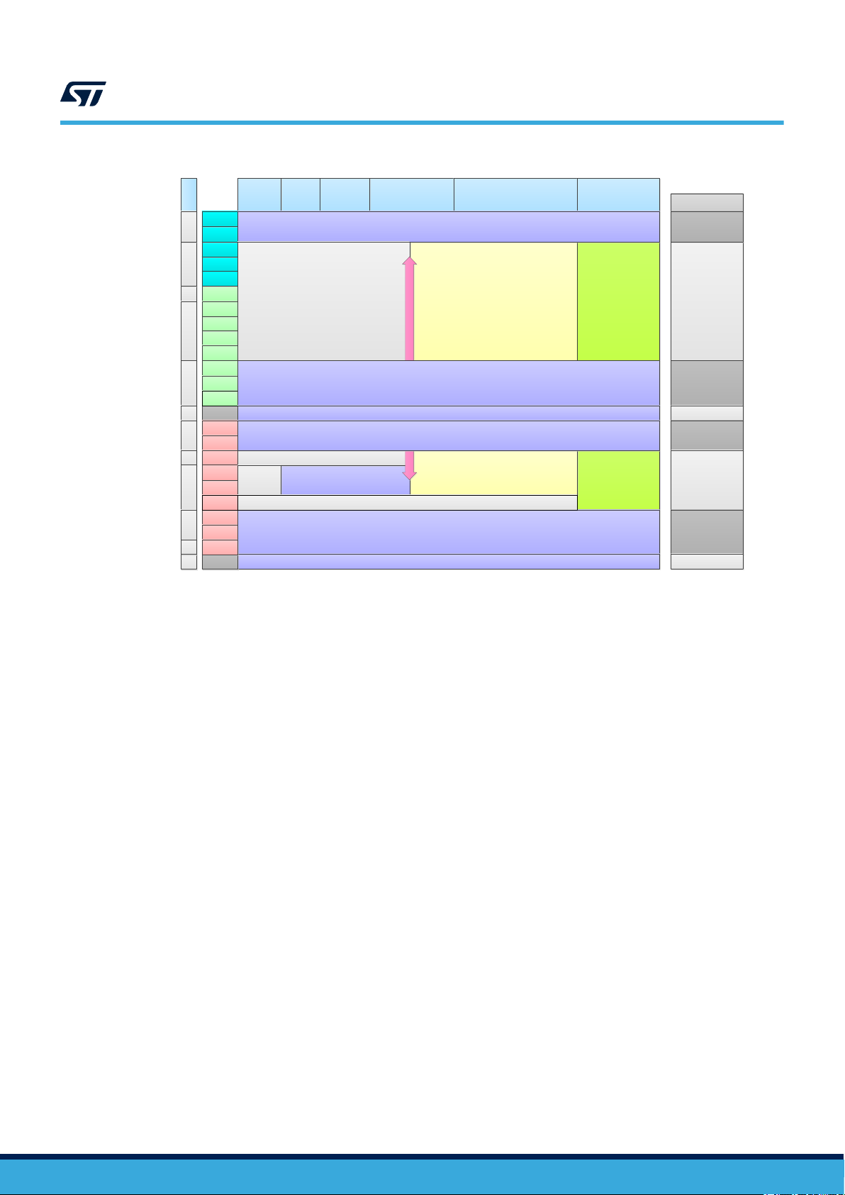
Figure 1. Voltage monitors functionality
TN1356
How to configure the LVDs/HVDs
Power ON
PH0D exit
(HSM)
exit
Destructive Reset (can be masked via Test Mode only)
NA
Voltage
Detector
UVD600_IF
VD15
UVD600_FL
LVD400_IF
VD14
LVD400_AS
LVD400_IM
VD13
HVD400_IF
LVD290_IF
LVD290_AS
VD11
LVD290_FL
LVD290_C
MVD270_FL
VD10
MVD270_C
MVD270_SB
VD8 NAPOR200_C
UVD140_FL
VD7
UVD140_C
HVD134_C
VD6
LVD100_FL
VD3
LVD100_C
LVD100_SB NA
MVD094_FA/FB
VD2
MVD094_C
MVD082T_C
VD1
VD0
POR031_C
PH1D
NA
NA
PH2Dto PH3D
Including trimming steps
Destructive Reset (can be masked via Test Mode only)
Destructive Reset reaction can be configured via DCF.
(If no DCF is programmed no reset reaction will occur)
Trimming done
Destructive Reset (can be masked via Test Mode only)
Destructive Reset
Destructive Reset (can be masked via Test Mode only)
Destructive Reset reaction can be configured via DCF.
(If no DCF is programmed no reset reaction will occur)
Destructive Reset (can be masked via Test Mode only)
Destructive Reset
PH1Fto PH3F Run-time
FCCU reaction is disabled.
Interrupt reaction is disabled.
FCCU reaction is disabled.
Interrupt reaction is disabled.
Reset-, FCCU- and Interrupt-reaction
can be changed via PMUdig and FCCU
registers
Reset-, FCCU- and Interrupt-reaction
can be changed via PMUdig and FCCU
registers
VD disabling
Test mode
Test mode or SW
Test mode
Test mode
Test mode or SW
Test mode
NA
1.3 How to configure the LVDs/HVDs
The HVD/LVD can be configured in two different ways:
• By hardware, configuring the PMC_REE_BUS DCF client
• By software, setting specific registers of the PMU_Dig interface
This choice is application dependent.
1.3.1 Hardware solution via PMC_REE_BUS DCF
The SPC58xx family supports a mechanism developed to handle the settings of the device parameters via data
stored in a OTP flash memory (UTEST Flash memory) and loaded during system boot, when the reset signal is
still asserted. At this scope the DCF records are used.
Note: OTP means One-Time-Programmable.
A DCF record consists of 2 of 32bit contiguous words:
1. the data to be written to a specific register
2. a pointer to the location of this register (DCF Chip Select [14:0] | DCF address [16:2] | 2b00)
All details about DCF and how it is used can be found at the section “Device Configuration Format (DCF)
Records” of the device Reference Manual (see Section A.1 Reference documents)
To unmask the LVDs/HVs reaction, the SPC58xx microcontrollers implement a specific Device Configuration
Format client: the PMC_REE_BUS, reset event enable.
Like other User DCF Records, the PMC_REE_BUS DCF record can be programmed by the user in UTEST
memory so to load the new device configuration right after Phase3[DEST] of the microcontroller boot sequence,
processed at the next reset event.
The PMC_REE_BUS DCF enables the generation of Reset event when the selected voltage passes the voltage
detection threshold.
Note: The voltage monitors and their associated levels for each device are given in device datasheet (see
Section A.1 Reference documents) referring to label "VD name".
TN1356 - Rev 1
page 4/15
Page 5
TN1356
How to configure the LVDs/HVDs
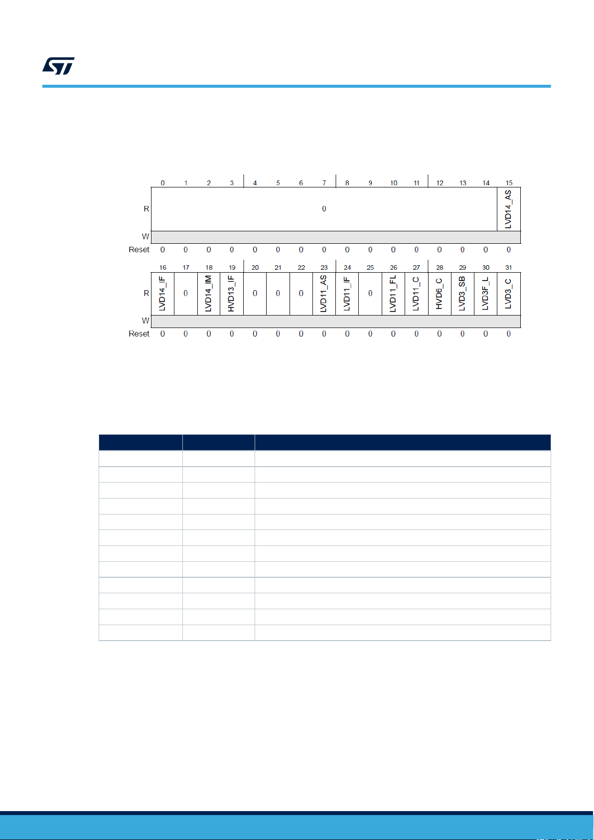
Just as an example, the Figure 2 shows the PMC_REE_BUS client and its bit fields for SPC58ECxx device.
Setting to “1” one of the available bitfields, the correspondent voltage threshold violation triggers a system reset
event.
Figure 2. PCM_REE_BUS client
The PMC REE_BUS pointer is 0x0100_0124 (CS|ADDR), in Section 2 LVD/HVD configuration examples an
example is available.
Table 2 describes the correspondence between the VD name (used in DS) and the bit name (LVDx_yy) of
PMC_REE_BUS DCF shown in Figure 2.
Table 2. VD number versus PMC_REE_BUS DCF
DCF bit name
LVD3_C LVD100_C LV detector asserts when PMU supply < 1.0 V
LVD3_C LVD100_FL LV detector asserts when FLASH supply < 1.0 V
LVD3_C LVD100_SB LV detector asserts when standby supply < 1.0 V
HVD6_C HVD134_C LV detector asserts when PMU supply > 1.34 V
LVD11_C LVD290_C HV detector asserts when PMU supply < 2.90 V
LVD11_FL LVD290_FL HV detector asserts when FLASH supply < 2.90 V
LVD11_IF LVD290_IF HV detector asserts when IO FLEXRAY supply < 2.90 V
LVD11_as LVD290_AS HV detector asserts when SAR ADC supply < 2.90 V
LVD13_IF HVD400_IF HV detector asserts when IO FLEXRAY supply > 4.00 V
LVD14_AS LVD400_AS HV detector asserts when SAR ADC supply < 4.00 V
LVD14_IF LVD400_IF HV detector asserts when IO FLEXRAY supply < 4.00 V
LVD14_IM LVD400_IM HV detector asserts when IO MAINS supply < 4.00 V
VD Name VD Meaning
TN1356 - Rev 1
Particular attention must be given at the correct programming of PMC_REE_BUS DCF, considering that when
RESET event is enabled by programming in UTEST, it cannot be disabled by software programming the
corresponding PMCDIG_REE_xx register.
When some bits of the PMC_REE DCF are set to “1” then the corresponding bits of PMCDIG_REE_LVx/PMCDIG
_REE_HVx registers in the PMC_Dig interface (Figure 3 shows PMCDIG_REE_LV0 register) are updated based
on the PMC_REE_BUS DCF value after the next boot sequence and these bits become “read only” bit, writing to
0 these bits have no effect.
In the aforementioned case, the voltage monitoring can be still disabled. The PMC_REE_BUS DCF must be
reprogrammed to mask the VDs and the new device configuration must be reloaded by a new boot sequence.
Loading the new value of PMC_REE_BUS DCF to disable the VDs, the corresponding bits of
PMCDIG_REE_LVx/PMCDIG _REE_HVx registers go back to be “read/write bit”.
page 5/15
Page 6

TN1356
How to configure the LVDs/HVDs
Figure 3. Reset Event Enable (REE_LV0)
1.3.2 Software solution via PMC_DIG interface
By default, the PCM_REE_BUS DCF does not enable any voltage detection:
• Reset value: PCM_REE_BUS DCF = 0x000_0000_00000_000
Therefore, the SW can program the voltage detection for each “configurable” LVD/HVD and its reaction (a RESET
event, FCCU event or interrupt) by means of control registers available in the Power Management Controller
digital interface (PMC_Dig).
The PMU_Dig interface includes the following registers for configuring LVD and HVD voltage detection:
• Reset Event Enable registers low voltage and High voltage (REE_LVx /REE_HVx, x = 0,1) that control
whether the voltage detect signal event causes a reset.
• Reset Event Select registers low voltage and High voltage (RES_LVx/ RES_HVx x = 0,1) that select
whether the voltage detect signal event causes a destructive or functional reset.
• FCCU Event Enable registers low voltage and High voltage (FEE_LVx/ FEE_HVx x = 0,1 ) that enable the
sending of event signal to the FCCU (Fault Collection and Control Unit) whether the voltage detect signal is
triggered.
• Interrupt Enable registers low voltage and High voltage (IE_LVx/IE_HV x = 0,1) that enable an interrupt in
case of the voltage detect signal event. A ‘0’ indicates that no interrupt is enabled, a ‘1’ indicates that an
interrupt is enabled.
Note: The PMCDIG_REE_LVx/HVx registers are not reset by a Destructive Reset but only by a POR reset event.
In details, the influence of reset on PMCDIG_YYY_xxx registers is:
• The POR reset is used on EPR_LVx, EPR_HVx, REE_LVx, REE_HVx, RES_LVx and RES_HVx registers.
• The destructive reset is used on REE_TD, RES_TD, FEE_LVx, FEE_HVx and FEE_TD registers.
• The functional reset is used on IE_HVx, IE_LVx, IE_G, CTL_TD registers.
Note: Temperature registers (xxx_TD) are not present on the SPC582Bxx device.
The present state of the voltage detect events for each of the supplies is reported in the Supply Gauge Status
Register (GR_S). Each bit is asserted when any of the voltage level falls below/rises above the corresponding
LVD/HVD threshold and clears when the supply rises above/falls below its corresponding LDV/HVD threshold.
TN1356 - Rev 1
page 6/15
Page 7

1.4 PMC_REE_BUS DCF vs PMCDIG registers
The relationship between bits of the PMC_REE_BUS DCF record and PMCDIG_REE_xxx registers is
summarized in the Table 3.
Table 3. PMC_REE_DCF vs PMCDIG_REExx
TN1356
PMC_REE_BUS DCF vs PMCDIG registers
PMC_REE_BUS
Bit
15 LVD14_AS REE_HV1[REE14_AS] LVD400_AS
16 LVD14_IF REE_HV1[REE14_IF] LVD400_IF
18 LVD14_IM REE_HV1[REE14_IM] LVD400_IM
19 HVD13_IF REE_HV1[REE13_IF] HVD400_IF
23 LVD11_AS REE_HV0[REE11_AS] LVD290_AS
24 LVD11_IF REE_HV0[REE11_IF] LVD290_IF
26 LVD11_FL REE_HV0[REE11_FL] LVD290_FL
27 LVD11_C REE_HV0[REE11_C] LVD290_C
28 HVD6_C REE_LV1[REE6_C] HVD134_C
29 LVD3_SB REE_LV0[REE3_SB] LVD100_SB
30 LVD3_FL REE_LV0[REE3_FL] LVD100_FL
31 LVD3_C REE_LV0[REE3_C] LVD100_C
PMC_REE_BUS Bit
name
PMCDIG_REE_xxx Bit
name
VD Name
(1)
VD Meaning
HV detector asserts when SAR ADC
supply < 4.00 V
HV detector asserts when IO
FLEXRAY supply < 4.00 V
HV detector asserts when IO MAINS
supply < 4.00 V
HV detector asserts when IO
FLEXRAY supply > 4.00 V
HV detector asserts when SAR ADC
supply < 2.90 V
HV detector asserts when IO
FLEXRAY supply < 2.90 V
HV detector asserts when FLASH
supply < 2.90 V
HV detector asserts when PMU supply
< 2.90 V
LV detector asserts when PMU supply
> 1.34 V
LV detector asserts when standby
supply < 1.0 V
LV detector asserts when FLASH
supply < 1.0 V
LV detector asserts when PMU supply
< 1.0 V
1. For more details and the whole list of voltage monitors, check the section “Voltage Monitors” in SPC58xx DSs (see
Section A.1 Reference documents).
TN1356 - Rev 1
page 7/15
Page 8

LVD/HVD configuration examples
2 LVD/HVD configuration examples
In this chapter some basic configuration examples of PMC_REE_BUS DCF and PMC_Dig interface for voltage
detection are given.
Programming LVD/HVD via PCM_REE_BUS
Example 1: PCM_REE_BUS record set to 0x0100_0124_0000_0001 (CS|ADDR|DATA)
Programming the PCM_REE_BUS DCF (see Figure 1) equal to 0x0100_0124_0000_0001, only the LVD3_C
VD is set. The result is to enable only the threshold for LVD100_C detector (refer to Table 2). The DCF client
configuration takes effect after the next boot sequence and in case the PMU supply is less than the relative
threshold value shown in the DS (for example 1.06 V < LVD100_C < 1.11 V), a reset event will be generated
without any programming of the PMC_Dig interface.
After loading the previous mentioned DCF configuration, the value of the PMCDIG_REE_LV0 register and the
PMCDIG_RES_LV0 register at POR is:
• PMCDIG_REE_LV0 = to 0x0000_0001_ 0000_0000 ( REE3_C bit is set to 1)
• PMCDIG_RES_LV0 = to 0x0000_0000_ 0000_0000 ( RES3_C bit is clear )
The REE3_C bit results “only readable”, while the other bits of PMCDIG_REE_LV0 register, REE3_SB and
REE3_FL are still programmable (writable) by SW. The Reset Event Select register (RES_LV0) selects by default
a destructive reset.
To sum up, in the Example 1:
• DCF client enables only the LVD3_C reset event and all other configurable LVD/HVD reset events are still
disabled by DCF.
• After next POR sequence (DCF configuration is loaded) the default value of PMU_Dig registers are:
– PMCDIG_REE_LV0[REE3_C] = 1 ( it cannot cleared → bit only read)
– PMCDIG_REE_LV0[LVDxx] = 0 ( bit writable) and
– PMCDIG_RES_LV0[LVDxx] = 0 ( bit writable)
Note: • In this example the user can still select the kind of reset, destructive or functional, configuring the
PMCDIG_RES_LV0 register, for more details refer to the register description in the device reference
manual.
• When a RESET event is enabled through the PCM_REE_BUS DCF record, it cannot be disabled by
clearing the correspondent bit in the PMC REE_XX register.
Programming VD via PMC_Dig.
Here below three examples assuming PCM_REE_BUS DCF at default value (equal to 0x0000_0000).
The PMC_Dig interface has the full control of voltage monitoring and the LVDs/HVDs trigger event reaction
depends on the programming of the PMC REE/RES/FEE/IE registers.
The User can enable the VD monitoring and select the kind of reset (functional or destructive reset) and/or enable
the reporting to FCCU and/or interrupt event.
Example 2: LVD100_C VD monitoring
A destructive reset is configured as reaction in case that the LVD100_C threshold is crossed. FCCU and interrupt
are disabled.
• PMCDIG_REE_LV0[REE3_C] = 1 (REE3_C reset enable, LVD100_C VD)
• PMCDIG_RES_LV0[RES3_C] = 0 (Destructive Reset Generated)
• PMCDIG_FEE_LV0[FEE3_C] = 0 (FEE3_C FCCU event disable)
• PMCDIG_IE_LV0[VD3IE3_C] = 0 (Interrupt disabled)
Example 3: LVD100_C VD FCCU event
A FCCU event is configured in case the LVD100_C threshold is crossed. The reset reaction and interrupt are
disabled.
• PMCDIG_REE_LV0[REE3_C] = 0 (REE3_C reset disable, LVD100_C VD)
• PMCDIG_RES_LV0[RES3_C] = 0 (Destructive Reset Generated)
• PMCDIG_FEE_LV0[FEE3_C] = 1 (FEE3_C FCCU
• PMCDIG_IE_LV0[VD3IE3_C] = 0 (Interrupt disabled)
(1)
event enable)
TN1356
TN1356 - Rev 1
page 8/15
Page 9

LVD/HVD configuration examples
1. Refer to table “FCCU failure inputs” in the device Reference Manual (see Section A.1 Reference documents).
Note: The FCCU reaction (IRQ, Short/Long Functional FCCU reset) must be configured by the FCCU module.
Example 4: LVD100_C VD Interrupt event
An interrupt event is configured in case the LVD100_C threshold is crossed. The reset reaction and FCCU event
are disabled.
• PMCDIG_REE_LV0[REE3_C] = 0 (REE3_C reset disable, LVD100_C VD)
• PMCDIG_RES_LV0[RES3_C] = 0 (Destructive Reset Generated)
• PMCDIG_FEE_LV0[FEE3_C] = 0 (FEE3_C FCCU event disabled)
• PMCDIG_IE_LV0[VD3IE3_C] = 1 (Interrupt
1. Refer to table “Interrupt sources” in the device Reference Manual (see Section A.1 Reference documents).
(1)
enabled)
TN1356
TN1356 - Rev 1
page 9/15
Page 10
Appendix A Other information
A.1 Reference documents
Doc Name ID Title
DS11597 029210 SPC58 2B Line - 32 bit Power Architecture automotive MCU Single core 80Mhz, 1MByte Flash, ASIL-B
DS11701 029439 32-bit Power Architecture microcontroller for automotive ASIL-B applications
DS11620 029264
DS11758 029572 32-bit Power Architecture microcontroller for automotive ASIL-D applications
DS11646 029333 32-bit Power Architecture microcontroller for automotive ASIL-D applications
DS12304 031027
DS11734 029507 32-bit Power Architecture microcontroller for automotive ASIL-D applications
RM0403 027949 SPC58 2B Line - 32 bit Power Architecture automotive MCU z2 core 80 MHz, 1 MByte Flash, ASIL-B
RM0449 030699
RM0407 028117
RM0391 027214
RM0452 031241
RM0421 028528 SPC58xNx 32-bit Power Architecture microcontroller for automotive ASILD applications
SPC58 C Line - 32 bit Power Architecture automotive MCU Dual z4 cores 180 MHz, 4 MBytes Flash,
HSM, ASIL-B
SPC58 H Line - 32 bit Power Architecture automotive MCU Triple z4 cores 200 MHz, 10 MBytes Flash,
HSM, ASIL-D
SPC584Bx 32-bit MCU family built on the Power Architecture for automotive body electronics
applications
SPC584Cx/SPC58ECx 32-bit MCU family built on the Power Architecture for automotive body
electronics applications
SPC58 E/G Line - 32 bit Power Architecture automotive MCU Triple z4 cores 180 MHz, 6 MBytes Flash,
HSM, ASIL-D
SPC58 H Line - 32 bit Power Architecture automotive MCU Triple z4 cores 200 MHz, 10 MBytes Flash,
HSM, ASIL-D
TN1356
Other information
Table 4. Reference documents
A.2 Acronyms
Acronym Name
DCF Device Configuration Format
PMC_Dig Power Management Controller digital interface
LVD Low voltage detection circuit
HVD High voltage detection circuit
UVD Upper Voltage Detector
MVD Minimum Voltage Detector
RGM Reset Generation Module
FCCU Fault Collection and Control Unit
Table 5. Acronyms
TN1356 - Rev 1
page 10/15
Page 11

Revision history
TN1356
Table 6. Document revision history
Date Version Changes
11-Feb-2021 1 Initial release.
TN1356 - Rev 1
page 11/15
Page 12

TN1356
Contents
Contents
1 Voltage monitoring ................................................................2
1.1 Overview .....................................................................2
1.2 LVD and HVD .................................................................3
1.3 How to configure the LVDs/HVDs .................................................4
1.3.1 Hardware solution via PMC_REE_BUS DCF ...................................4
1.3.2 Software solution via PMC_DIG interface ......................................6
1.4 PMC_REE_BUS DCF vs PMCDIG registers ........................................7
2 LVD/HVD configuration examples ..................................................8
Appendix A Other information ........................................................10
A.1 Reference documents..........................................................10
A.2 Acronyms ....................................................................10
Revision history .......................................................................11
TN1356 - Rev 1
page 12/15
Page 13

TN1356
List of tables
List of tables
Table 1. Voltage monitors configurability ..........................................................2
Table 2. VD number versus PMC_REE_BUS DCF ...................................................5
Table 3. PMC_REE_DCF vs PMCDIG_REExx...................................................... 7
Table 4. Reference documents ............................................................... 10
Table 5. Acronyms ........................................................................ 10
Table 6. Document revision history ............................................................. 11
TN1356 - Rev 1
page 13/15
Page 14

TN1356
List of figures
List of figures
Figure 1. Voltage monitors functionality ..........................................................4
Figure 2. PCM_REE_BUS client............................................................... 5
Figure 3. Reset Event Enable (REE_LV0) ........................................................6
TN1356 - Rev 1
page 14/15
Page 15

TN1356
IMPORTANT NOTICE – PLEASE READ CAREFULLY
STMicroelectronics NV and its subsidiaries (“ST”) reserve the right to make changes, corrections, enhancements, modifications, and improvements to ST
products and/or to this document at any time without notice. Purchasers should obtain the latest relevant information on ST products before placing orders. ST
products are sold pursuant to ST’s terms and conditions of sale in place at the time of order acknowledgement.
Purchasers are solely responsible for the choice, selection, and use of ST products and ST assumes no liability for application assistance or the design of
Purchasers’ products.
No license, express or implied, to any intellectual property right is granted by ST herein.
Resale of ST products with provisions different from the information set forth herein shall void any warranty granted by ST for such product.
ST and the ST logo are trademarks of ST. For additional information about ST trademarks, please refer to www.st.com/trademarks. All other product or service
names are the property of their respective owners.
Information in this document supersedes and replaces information previously supplied in any prior versions of this document.
© 2021 STMicroelectronics – All rights reserved
TN1356 - Rev 1
page 15/15
 Loading...