

PM6686
Dual step-down controller with adjustable voltages, adjustable LDO
and auxiliary charge pump controller for notebook
Features
■ 5.5 V to 28 V input voltage range
■ Dual fixed OUT1 = 1.5 V/5 V and OUT2 =
1.05 V / 3.3 V outputs or adjustable OUT1 = 0.7
V to 5.5 V and OUT2 = 0.7 V to 2.5 V outputs,
± 1.5% accuracy over valley regulation
■ Low-side MOSFETs' R
current sensing
DS(on)
and programmable current limit
■ Constant ON-time control
■ Frequency selectable
■ Soft-start internally fixed at 2 ms and soft-stop
■ Selectable pulse skipping at light loads
■ Selectable minimum frequency (33 kHz) in
pulse skip mode
■ Independent Power Good and EN signals
■ Latched OVP and UVP
■ Charge pump feedback
■ Fixed 3.3 V/5.0 V, or adjustable output 0.7 V to
4.5 V, ± 1.5% (LDO): 200 mA
■ 3.3 V reference voltage ± 2.0%: 5 mA
■ 2.0 V reference voltage ± 1.0%: 50 µA
Applications
■ Notebook computers
■ Main (3.3 V/5 V), chipset (1.5 V/1.05 V),
DDR1/2/3, graphic cards power supply
■ PDAs, mobile devices, tablet PC or slates
■ 3-4 cells Li+ battery powered devices
Description
PM6686 is a dual step-down controller specifically
designed to provide extremely high efficiency
conversion, with lossless current sensing
technique. The constant on-time architecture
assures fast load transient response and the
embedded voltage feed-forward provides nearly
constant switching frequency operation. Pulse
skipping technique increases efficiency at very
light load. Moreover a minimum switching
frequency of 33 kHz is selectable to avoid audio
noise issues. The PM6686 provides a selectable
switching frequency, allowing three different
values of switching frequencies for the two
switching sections. The output voltages OUT1
and OUT2 can be programmed to regulate
1.5 V/5 V and 1.05 V/3.3 V outputs respectively or
can deliver two adjustable output voltages. An
optional external charge pump can be monitored.
This device embeds a linear regulator that can
provide 3.3 V/5 V or an adjustable voltage from
0.7 V to 4.5 V output. The linear regulator
provides up to 100 mA output current. LDO can
be bypassed with the switching regulator outputs
or with an external power supply (switchover
function).
VFQFPN-32 5 x 5 mm
When in switchover, the LDO output can source
up to 200 mA.
Table 1. Device summary
July 2009 Doc ID 15281 Rev 4 1/50
Order codes Package Packaging
PM6686
Tr ay
VFQFPN-32L 5 x 5 mm
PM6686TR Tape and reel
www.st.com
50

Contents PM6686
Contents
1 Simplified application schematic . . . . . . . . . . . . . . . . . . . . . . . . . . . . . . . 6
2 Pin settings . . . . . . . . . . . . . . . . . . . . . . . . . . . . . . . . . . . . . . . . . . . . . . . . 7
2.1 Connections . . . . . . . . . . . . . . . . . . . . . . . . . . . . . . . . . . . . . . . . . . . . . . . . 7
2.2 Pin descriptions . . . . . . . . . . . . . . . . . . . . . . . . . . . . . . . . . . . . . . . . . . . . . 7
3 Electrical data . . . . . . . . . . . . . . . . . . . . . . . . . . . . . . . . . . . . . . . . . . . . . 10
3.1 Maximum rating . . . . . . . . . . . . . . . . . . . . . . . . . . . . . . . . . . . . . . . . . . . . 10
3.2 Thermal data . . . . . . . . . . . . . . . . . . . . . . . . . . . . . . . . . . . . . . . . . . . . . . 10
4 Recommended operating conditions . . . . . . . . . . . . . . . . . . . . . . . . . . 11
5 Electrical characteristics . . . . . . . . . . . . . . . . . . . . . . . . . . . . . . . . . . . . 12
6 Typical operating characteristics . . . . . . . . . . . . . . . . . . . . . . . . . . . . . 15
6.1 Screen shots . . . . . . . . . . . . . . . . . . . . . . . . . . . . . . . . . . . . . . . . . . . . . . 19
7 Block diagram . . . . . . . . . . . . . . . . . . . . . . . . . . . . . . . . . . . . . . . . . . . . . 23
8 Device description . . . . . . . . . . . . . . . . . . . . . . . . . . . . . . . . . . . . . . . . . 24
8.1 Switching sections . . . . . . . . . . . . . . . . . . . . . . . . . . . . . . . . . . . . . . . . . . 24
8.1.1 Output voltage set up . . . . . . . . . . . . . . . . . . . . . . . . . . . . . . . . . . . . . . . 24
8.1.2 Constant on time control (COT) . . . . . . . . . . . . . . . . . . . . . . . . . . . . . . . 26
8.1.3 PWM . . . . . . . . . . . . . . . . . . . . . . . . . . . . . . . . . . . . . . . . . . . . . . . . . . . 28
8.1.4 SKIP . . . . . . . . . . . . . . . . . . . . . . . . . . . . . . . . . . . . . . . . . . . . . . . . . . . . 29
8.1.5 Non audible SKIP (NA SKIP) . . . . . . . . . . . . . . . . . . . . . . . . . . . . . . . . . 29
8.1.6 Gate drivers and logic supply . . . . . . . . . . . . . . . . . . . . . . . . . . . . . . . . 30
8.1.7 Current sensing and current limit . . . . . . . . . . . . . . . . . . . . . . . . . . . . . . 31
8.1.8 Soft-start and soft-end . . . . . . . . . . . . . . . . . . . . . . . . . . . . . . . . . . . . . . 32
9 Monitoring and protections . . . . . . . . . . . . . . . . . . . . . . . . . . . . . . . . . . 34
9.1 Overvoltage protection . . . . . . . . . . . . . . . . . . . . . . . . . . . . . . . . . . . . . . . 34
9.2 Undervoltage protection . . . . . . . . . . . . . . . . . . . . . . . . . . . . . . . . . . . . . . 34
9.3 PVCC monitor . . . . . . . . . . . . . . . . . . . . . . . . . . . . . . . . . . . . . . . . . . . . . 34
2/50 Doc ID 15281 Rev 4

PM6686 Contents
9.4 Linear regulator section . . . . . . . . . . . . . . . . . . . . . . . . . . . . . . . . . . . . . . 35
9.5 Charge pump . . . . . . . . . . . . . . . . . . . . . . . . . . . . . . . . . . . . . . . . . . . . . . 36
9.6 Voltage references . . . . . . . . . . . . . . . . . . . . . . . . . . . . . . . . . . . . . . . . . . 37
9.7 General device fault management . . . . . . . . . . . . . . . . . . . . . . . . . . . . . . 37
9.7.1 Thermal protection . . . . . . . . . . . . . . . . . . . . . . . . . . . . . . . . . . . . . . . . . 37
10 Application information . . . . . . . . . . . . . . . . . . . . . . . . . . . . . . . . . . . . . 38
10.1 External components selection . . . . . . . . . . . . . . . . . . . . . . . . . . . . . . . . 38
10.1.1 Inductor . . . . . . . . . . . . . . . . . . . . . . . . . . . . . . . . . . . . . . . . . . . . . . . . . 38
10.1.2 Input capacitor . . . . . . . . . . . . . . . . . . . . . . . . . . . . . . . . . . . . . . . . . . . . 39
10.1.3 Output capacitor . . . . . . . . . . . . . . . . . . . . . . . . . . . . . . . . . . . . . . . . . . 39
10.1.4 MOSFET . . . . . . . . . . . . . . . . . . . . . . . . . . . . . . . . . . . . . . . . . . . . . . . . 40
11 Diode selection . . . . . . . . . . . . . . . . . . . . . . . . . . . . . . . . . . . . . . . . . . . . 42
11.1 Freewheeling diode . . . . . . . . . . . . . . . . . . . . . . . . . . . . . . . . . . . . . . . . . 42
11.2 Charge pump diode . . . . . . . . . . . . . . . . . . . . . . . . . . . . . . . . . . . . . . . . . 42
11.3 Other important components . . . . . . . . . . . . . . . . . . . . . . . . . . . . . . . . . . 43
11.3.1 VIN filter . . . . . . . . . . . . . . . . . . . . . . . . . . . . . . . . . . . . . . . . . . . . . . . . . 43
11.3.2 PVCC and VCC . . . . . . . . . . . . . . . . . . . . . . . . . . . . . . . . . . . . . . . . . . . 43
11.3.3 VREF2 and VREF3 capacitors . . . . . . . . . . . . . . . . . . . . . . . . . . . . . . . 44
11.3.4 LDO output capacitors . . . . . . . . . . . . . . . . . . . . . . . . . . . . . . . . . . . . . . 44
11.3.5 Bootstrap circuit . . . . . . . . . . . . . . . . . . . . . . . . . . . . . . . . . . . . . . . . . . . 44
12 PCB design guidelines . . . . . . . . . . . . . . . . . . . . . . . . . . . . . . . . . . . . . . 45
13 Package mechanical data . . . . . . . . . . . . . . . . . . . . . . . . . . . . . . . . . . . . 47
14 Revision history . . . . . . . . . . . . . . . . . . . . . . . . . . . . . . . . . . . . . . . . . . . 49
Doc ID 15281 Rev 4 3/50

List of figures PM6686
List of figures
Figure 1. Simplified application schematic . . . . . . . . . . . . . . . . . . . . . . . . . . . . . . . . . . . . . . . . . . . . . . 6
Figure 2. Pin connection (through top view) . . . . . . . . . . . . . . . . . . . . . . . . . . . . . . . . . . . . . . . . . . . . 7
Figure 3. Efficiency vs load OUT1 = 5 V, TON = VCC. . . . . . . . . . . . . . . . . . . . . . . . . . . . . . . . . . . . 15
Figure 4. Efficiency vs load OUT2 = 3.3 V, TON = VCC . . . . . . . . . . . . . . . . . . . . . . . . . . . . . . . . . . 15
Figure 5. Efficiency vs load OUT1 = 1.5 V, TON = VCC . . . . . . . . . . . . . . . . . . . . . . . . . . . . . . . . . . 15
Figure 6. Efficiency vs load OUT2 = 1.05 V, TON = VCC . . . . . . . . . . . . . . . . . . . . . . . . . . . . . . . . . 15
Figure 7. Load regulationOUT1 = 5 V, TON = VCC. . . . . . . . . . . . . . . . . . . . . . . . . . . . . . . . . . . . . . 16
Figure 8. Load regulationOUT2 = 3.3 V, TON = VCC . . . . . . . . . . . . . . . . . . . . . . . . . . . . . . . . . . . . 16
Figure 9. Load regulation OUT1 = 1.5 V, TON = VCC. . . . . . . . . . . . . . . . . . . . . . . . . . . . . . . . . . . . 16
Figure 10. Load regulation OUT2 = 1.05 V, TON = VCC. . . . . . . . . . . . . . . . . . . . . . . . . . . . . . . . . . . 16
Figure 11. Switching frequency vs load OUT1 = 5 V, TON = VCC . . . . . . . . . . . . . . . . . . . . . . . . . . . 16
Figure 12. Switching frequency vs load OUT2 = 3.3 V, TON = VCC . . . . . . . . . . . . . . . . . . . . . . . . . . 16
Figure 13. Section 1 line regulation OUT1 = 5 V, TON = VCC . . . . . . . . . . . . . . . . . . . . . . . . . . . . . . 17
Figure 14. Section 2 line regulation OUT2 = 3.3 V, TON = VCC . . . . . . . . . . . . . . . . . . . . . . . . . . . . . 17
Figure 15. Section 1 line regulation OUT1 = 1,5 V, TON = VCC . . . . . . . . . . . . . . . . . . . . . . . . . . . . . 17
Figure 16. Section 2 line regulation OUT2 = 1,05 V, TON = VCC . . . . . . . . . . . . . . . . . . . . . . . . . . . . 17
Figure 17. Stand-by mode input battery current vs input voltage . . . . . . . . . . . . . . . . . . . . . . . . . . . . 17
Figure 18. Shut-down mode input battery current vs input voltage . . . . . . . . . . . . . . . . . . . . . . . . . . . 17
Figure 19. PWM no load input currents vs input voltage . . . . . . . . . . . . . . . . . . . . . . . . . . . . . . . . . . . 18
Figure 20. SKIP no load input currents vs input voltage . . . . . . . . . . . . . . . . . . . . . . . . . . . . . . . . . . . 18
Figure 21. NA SKIP no load input currents vs input voltage . . . . . . . . . . . . . . . . . . . . . . . . . . . . . . . . 18
Figure 22. VREF3 load regulation . . . . . . . . . . . . . . . . . . . . . . . . . . . . . . . . . . . . . . . . . . . . . . . . . . . . 18
Figure 23. VREF2 load regulation . . . . . . . . . . . . . . . . . . . . . . . . . . . . . . . . . . . . . . . . . . . . . . . . . . . . 18
Figure 24. LDO = 3,3 V load regulation . . . . . . . . . . . . . . . . . . . . . . . . . . . . . . . . . . . . . . . . . . . . . . . . 18
Figure 25. LDO = 5 V load regulation . . . . . . . . . . . . . . . . . . . . . . . . . . . . . . . . . . . . . . . . . . . . . . . . . 19
Figure 26. OUT1 soft-start no load . . . . . . . . . . . . . . . . . . . . . . . . . . . . . . . . . . . . . . . . . . . . . . . . . . . 19
Figure 27. OUT2 soft-start no load . . . . . . . . . . . . . . . . . . . . . . . . . . . . . . . . . . . . . . . . . . . . . . . . . . . 19
Figure 28. OUT1 soft-start 8 A constant current load . . . . . . . . . . . . . . . . . . . . . . . . . . . . . . . . . . . . . 20
Figure 29. OUT2 soft-start loaded 8 A constant current load . . . . . . . . . . . . . . . . . . . . . . . . . . . . . . . 20
Figure 30. OUT1 soft-end, no load . . . . . . . . . . . . . . . . . . . . . . . . . . . . . . . . . . . . . . . . . . . . . . . . . . . 20
Figure 31. OUT2 soft-end, no load . . . . . . . . . . . . . . . . . . . . . . . . . . . . . . . . . . . . . . . . . . . . . . . . . . . 20
Figure 32. OUT1 soft-start, EN2 = VREF2 no loads applied . . . . . . . . . . . . . . . . . . . . . . . . . . . . . . . . 20
Figure 33. OUT2 soft-start, EN1=VREF2 no loads applied . . . . . . . . . . . . . . . . . . . . . . . . . . . . . . . . . 20
Figure 34. soft-end, EN2 = VREF2 no loads applied . . . . . . . . . . . . . . . . . . . . . . . . . . . . . . . . . . . . . . 21
Figure 35. soft-end, EN1=VREF2 no loads applied . . . . . . . . . . . . . . . . . . . . . . . . . . . . . . . . . . . . . . . 21
Figure 36. Load transient 0-5 A 2 A/µs OUT1 = 5 V PWM mode . . . . . . . . . . . . . . . . . . . . . . . . . . . . 21
Figure 37. Load transient 0-5 A 2 A/µs OUT1 = 5 V SKIP mode . . . . . . . . . . . . . . . . . . . . . . . . . . . . . 21
Figure 38. Load transient 0-5 A 2 A/ µs OUT1 = 1,5 V PWM mode . . . . . . . . . . . . . . . . . . . . . . . . . . 21
Figure 39. Load transient 0-5 A 2 A/ µs OUT1 = 1,5 V SKIP mode . . . . . . . . . . . . . . . . . . . . . . . . . . . 21
Figure 40. Load transient 0-5 A 2 A/µs OUT2 = 3.3 V PWM mode . . . . . . . . . . . . . . . . . . . . . . . . . . . 22
Figure 41. Load transient 0-5 A 2 A/µs OUT2 = 3.3 V SKIP mode . . . . . . . . . . . . . . . . . . . . . . . . . . . 22
Figure 42. Load transient 0-5 A 2 A/ µs OUT2 = 1,05 V PWM mode . . . . . . . . . . . . . . . . . . . . . . . . . 22
Figure 43. Load transient 0-5 A 2 A/ µs OUT2 = 1,05 V SKIP mode . . . . . . . . . . . . . . . . . . . . . . . . . . 22
Figure 44. Functional block diagram . . . . . . . . . . . . . . . . . . . . . . . . . . . . . . . . . . . . . . . . . . . . . . . . . . 23
Figure 45. Resistor divider to configure the output voltage . . . . . . . . . . . . . . . . . . . . . . . . . . . . . . . . . 25
Figure 46. Constant on time block diagram . . . . . . . . . . . . . . . . . . . . . . . . . . . . . . . . . . . . . . . . . . . . . 27
Figure 47. Inductor current and output voltage in PWM mode . . . . . . . . . . . . . . . . . . . . . . . . . . . . . . 28
Figure 48. Inductor current and output voltage in SKIP mode . . . . . . . . . . . . . . . . . . . . . . . . . . . . . . 29
4/50 Doc ID 15281 Rev 4

PM6686 List of figures
Figure 49. Inductor current and output voltage in NA SKIP mode . . . . . . . . . . . . . . . . . . . . . . . . . . . . 30
Figure 50. Internal supply diagram . . . . . . . . . . . . . . . . . . . . . . . . . . . . . . . . . . . . . . . . . . . . . . . . . . . 31
Figure 51. Current waveforms in current limit conditions . . . . . . . . . . . . . . . . . . . . . . . . . . . . . . . . . . . 31
Figure 52. Current limit circuit block diagram. . . . . . . . . . . . . . . . . . . . . . . . . . . . . . . . . . . . . . . . . . . . 32
Figure 53. VOUT2 behavior if EN2 is connected to VREF2 . . . . . . . . . . . . . . . . . . . . . . . . . . . . . . . . 33
Figure 54. Charge pump application circuit . . . . . . . . . . . . . . . . . . . . . . . . . . . . . . . . . . . . . . . . . . . . . 36
Figure 55. VIN pin filter . . . . . . . . . . . . . . . . . . . . . . . . . . . . . . . . . . . . . . . . . . . . . . . . . . . . . . . . . . . . 43
Figure 56. VCC and PVCC filters. . . . . . . . . . . . . . . . . . . . . . . . . . . . . . . . . . . . . . . . . . . . . . . . . . . . . 43
Figure 57. Bootstrap circuit . . . . . . . . . . . . . . . . . . . . . . . . . . . . . . . . . . . . . . . . . . . . . . . . . . . . . . . . . 44
Figure 58. Current paths, ground connection and driver traces layout . . . . . . . . . . . . . . . . . . . . . . . . 46
Figure 59. Package dimensions. . . . . . . . . . . . . . . . . . . . . . . . . . . . . . . . . . . . . . . . . . . . . . . . . . . . . . 48
Doc ID 15281 Rev 4 5/50
Simplified application schematic PM6686
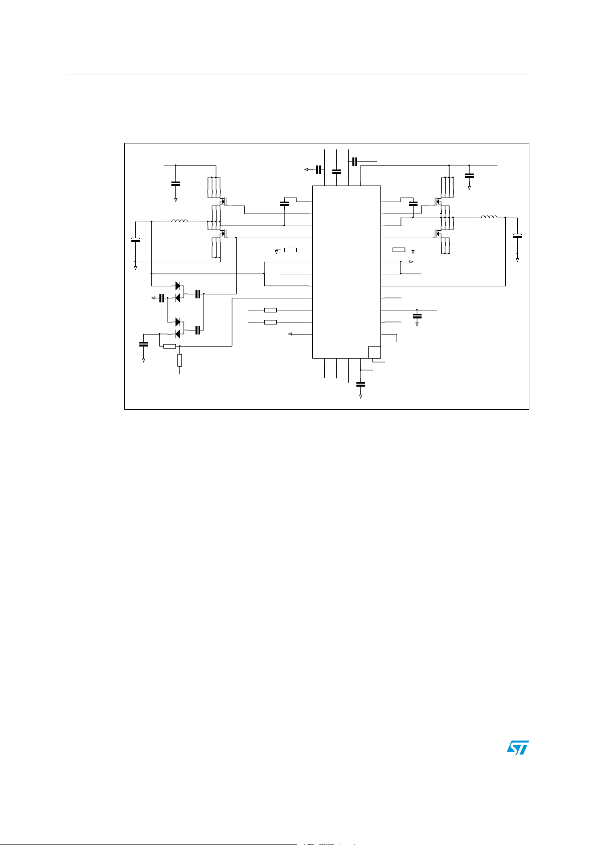
1 Simplified application schematic
Figure 1. Simplified application schematic
62%&
06##
62%&2%&
3'.$
"//4
('!4%
0(!3%
,'!4%
),)-
/54
&"
,$/?37
#0?&"
0'
0'
3+)0
3'.$
06##
0-
%.
2%&
6##
6).
5
6).
6##
62%&
%.
4/.
"//4
('!4%
0(!3%
,'!4%
),)-
0'.$
'.$
/54
2%&).
,$/2%&) .
%.?,$/
62%&
2%&
3'.$
6##
,$/
3'.$
62%&
0!$
3'.$
0'.$
0'.$
3'.$
06##
0'.$
0'.$
0'.$
6).
0'.$
0'.$
0'.$
3'.$
6##
6##
3'.$
0'.$
3'.$
0'.$
3'.$
!-V
6/50 Doc ID 15281 Rev 4
PM6686 Pin settings
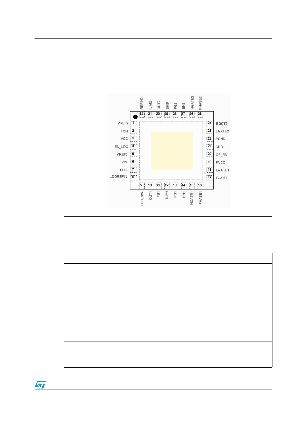
2 Pin settings
2.1 Connections
Figure 2. Pin connection (through top view)
0-
2.2 Pin descriptions
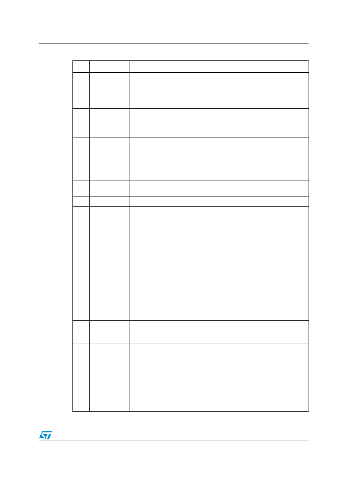
Table 2. Pin descriptions
N° Pin Function
1VREF2
2TON
3 VCC Controller supply voltage input. Bypass to GND with a 1 μF capacitor.
4EN_LDO
5VREF3
6VIN
!-V
Internal 2 V high accuracy voltage reference. It can deliver 50 μA. Loading
VREF2 can affect FB and output accuracy. Bypass to GND with a 100 nF
capacitor.
Frequency selection pin. It provides a selectable switching frequency,
allowing three different values of switching frequencies for the switching
sections.
Enable input for the linear regulator. The LDO is enabled if
EN_LDO is > 1.6 V and is disabled if EN_LDO < 1 V.
Internal 3.3 V high accuracy voltage reference. It can deliver 5 mA if
bypassed to GND with a 10 nF capacitor. If not used, it can be left floating.
Device supply voltage pin. VIN is used in the on-time generators of the two
switching controllers. VIN is also used to power the linear regulator when the
switchover function is not active. Connect VIN to the battery input and
bypass with a 1 µF capacitor.
Doc ID 15281 Rev 4 7/50
Pin settings PM6686
Table 2. Pin descriptions (continued)
N° Pin Function
Linear regulator output. It can provide up to 100 mA peak current. The LDO
regulates at 5 V If LDOREFIN is connected to GND. When the LDO is set at
5 V and LDO_SW is within 5 V switchover threshold, the internal regulator
shuts down and the LDO output pin is connected to LDO_SW through a
7LDO
8 LDOREFIN
9LDO_SW
10 OUT1
0.8 Ω switch. The LDO regulates at 3.3 V if LDOREFIN is connected to
VCC. When the LDO is set at 3.3 V and LDO_SW is within 3.3 V switchover
threshold, the internal regulator shuts down and the LDO output pin is
connected to LDO_SW through a 1.1 Ω switch. Bypass LDO output to GND
with a minimum of 4.7 µF ceramic capacitor.
Feedback of the adjustable linear regulator. Connect LDOREFIN to GND for
fixed 5 V operation. Connect LDOREFIN to VCC for fixed 3.3 V operation.
LDOREFIN can be used to program LDO output voltage from 0.7 V to 4.5 V:
LDO output is two times the voltage of LDOREFIN. The switchover function
is disabled in adjustable mode.
Source of the switchover connection. LDO_SW is the switchover source
voltage for the LDO when LDOREFIN is connected to GND or VCC.
Connect LDO_SW to 5 V if LDOREFIN is tied to GND. Connect LDO_SW to
3.3 V if LDOREFIN is tied to VCC.
Output voltage sense for the switching section 1.This pin must be directly
connected to the output voltage of the switching section. It provides also the
feedback for the switching section 1 when FB1 is tied to GND/VCC.
Feedback input for the switching section 1:
– If this pin is connected to GND, OUT1 operates at 5 V
11 FB1
– If this pin is connected to VCC, OUT1 operates at 1.5 V
– This pin is connected to a resistive voltage-divider from OUT1 to GND to
adjust the output voltage from 0.7 V to 5.5 V.
12 ILIM1
Positive current sense input for the switching section 1. It is possible to set a
threshold voltage that is compared with 1/10
th
of the GND-PHASE1 drop
during the off time.
Power Good output signal for the section 1. This pin is an open drain output
13 PG1
and It is pulled down when the output of the switching section 1 is out of
+/- 10% of its nominal value.
Enable input for the switching section 1.
– If EN1 < 0.8 V the switching section OUT1 is turned off and all faults are
14 EN1
cleared.
– If EN1 > 2.4 V the switching section OUT1 is turned on.
– If EN1 is connected to VREF2, the switching section OUT1 turns on after
the switching section OUT2 reaches regulation.
15 HGATE1 High-side gate driver output for section 1.
16 PHASE1
17 BOOT1
Switch node connection and return path for the high-side driver for the
section 1.It is also used as positive and negative current sense input.
Bootstrap capacitor connection for the switching section 1. It supplies the
high-side gate driver.
18 LGATE1 Low-side gate driver output for the section 1.
19 PVCC
5 V low-side gate drivers supply voltage input. Bypass to PGND with a 1 μF
capacitor.
8/50 Doc ID 15281 Rev 4
PM6686 Pin settings
Table 2. Pin descriptions (continued)
N° Pin Function
The CP_FB is used to monitor the optional external 14 V charge pump.
Connect a resistive voltage-divider from 14 V charge pump output to GND. If
20 CP_FB
21 GND
22 PGND
23 LGATE2 Low-side gate driver output for the section 2.
24 BOOT2
25 PHASE2
26 HGATE2 High-side gate driver output for section 2.
27 EN2
28 PG2
29 SKIP
30 OUT2
31 ILIM2
32 REFIN2
CP_FB drops below the threshold voltage, the device performs a no audible
skip cycle. This charges the charge pump output (driven by LGATE1). Leave
CP_FB floating if the charge pump feedback is not needed.
Signal ground reference for internal logic circuitry and LDO. It must be
connected to the signal ground plan of the power supply and to the exposed
pad. The signal ground plan and the power ground plan must be connected
together in one point near the PGND pin.
Power ground. This pin must be connected to the power ground plan of the
power supply.
Bootstrap capacitor connection for the switching section 2. It supplies the
high-side gate driver.
Switch node connection and return path for the high-side driver for the
section 2. It is also used as positive and negative current sense input.
Enable input for the switching section 2.
– If EN2 < 0.8 V the switching section OUT2 is turned off and all faults are
cleared.
– If EN2 > 2.4 V the switching section OUT2 is turned on.
If EN2 is connected to VREF2, the switching section OUT2 turns on after
the switching section OUT1 reaches regulation.
Power Good output signal for the section 2. This pin is an open drain output
and It is pulled down when the output of the switching section 2 is out of
+ 14% / - 10% of its nominal value.
Pulse skipping mode control input.
– If the pin is connected to VCC the PWM mode is enabled.
– If the pin is connected to GND, the pulse skip mode is enabled.
– If the pin is connected to VREF2 (or floating) the pulse skip mode is
enabled but and the switching frequency is kept higher than 33 kHz (No-
audible pulse skip mode).
Output voltage sense for the switching section 2.This pin must be directly
connected to the output voltage of the switching section. It provides also the
feedback for the switching section 2 when REFIN2 is tied to VREF3/VCC.
Positive current sense input for the switching section 2. It is possible to set a
threshold voltage that is compared with 1/10
th
of the GND-PHASE2 drop
during the off time.
Feedback input for the switching section 2:
– If this pin is connected to VCC, OUT2 operates at 3.3 V
– If this pin is connected to VREF3, OUT2 operates at 1.05 V
– If this pin is connected to an external reference from 0.7 V to 2.5 V, OUT2
works in tracking with this reference. Bypass REFIN2 to GND with a 100
nF capacitor.
Doc ID 15281 Rev 4 9/50
Electrical data PM6686
3 Electrical data
3.1 Maximum rating
Table 3. Absolute maximum ratings
Parameter Value Unit
VIN to PGND -0.3 to 38 V
PHASEx to PGND -0.3 to 38 V
BOOTx to PHASEx -0.3 to 6 V
PVCC to PGND -0.3 to 6 V
HGATEx to PHASEx -0.3 to BOOTx +0.3 V
LGATEx, CP_FB to PGND -0.3 to PVCC +0.3 V
VCC, ENx, SKIP, PGx, LDO, REFIN2, OUTx, VREF3,
LDOREFIN, LDO_SW, TON to GND
FB1, ILIMx to GND -0.3 to VCC+0.3 V
EN_LDO to GND -0.3 to 7 V
-0.3 to 6 V
VREF2 to GND -0.3 to VREF3+0.3 V
PGND to GND -0.3 to +0.3 V
Power dissipation at T
Maximum withstanding voltage range test condition: CDF-AECQ100-002- “human body model” acceptance criteria: “normal
performance”
3.2 Thermal data
Table 4. Thermal data
Symbol Parameter Value Unit
R
thJA
T
J
T
STG
Operating ambient temperature range -40 to 85 °C
T
A
Thermal resistance junction to ambient 35 °C/W
Junction operating temperature range -40 to 125 °C
Storage temperature range -50 to 150 °C
= 25 °C 2 W
A
±1250 V
10/50 Doc ID 15281 Rev 4
PM6686 Recommended operating conditions
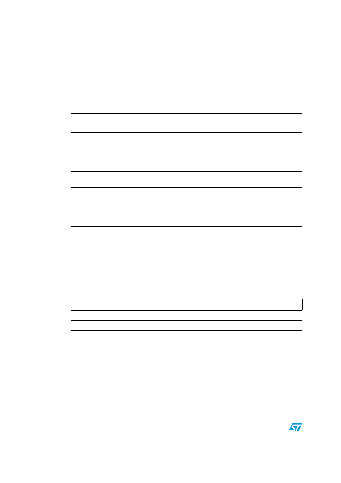
4 Recommended operating conditions
Table 5. Recommended operating conditions
Val ue
Symbol Parameter
Min Typ Max
VIN Input voltage range, LDO = 5 V in regulation 5.5 - 28 V
VCC VCC operative voltage range 4.5 - 5.5 V
REFIN2
REFIN2 voltage range with OUT2 in
adjustable mode, VIN = 5.5 V to 28 V
0.7 - 2.5 V
OUT1 OUT1 output voltage range 0.70 - 5.50 V
ILIM ILIM voltage range 0.2 - 2 V
Unit
LDOREFIN
LDO DC output current
(switchover function
enabled)
LDO DC output current
(switchover function
disabled)
LDOREFIN setting with LDO = 2 x LDOREFIN
(adjustable mode)
VIN = 5.5 V to 28 V, LDO_SW = 5 V,
LDOREFIN = GND
VIN = 5.5 V to 28 V, LDO_SW = 3.3 V,
LDOREFIN = VCC
VIN = 5.5 V to 28 V, LDO_SW = 0 V,
LDOREFIN = GND, VCC
0.35 - 2.25 V
- 200 mA
- 100 mA
- 100 mA
Doc ID 15281 Rev 4 11/50
Electrical characteristics PM6686
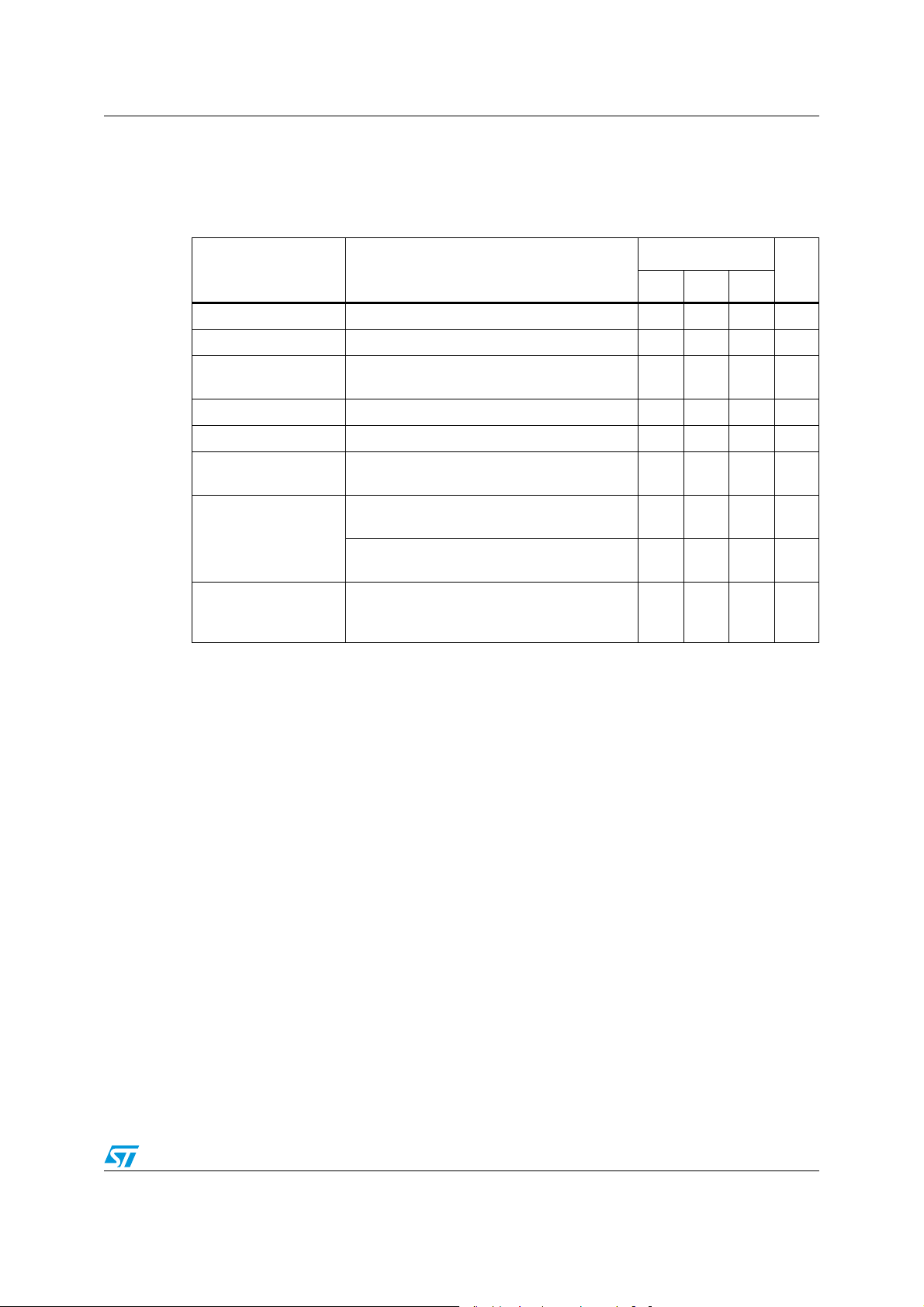
5 Electrical characteristics
VIN = 12 V, no load on LDO, OUT1, OUT2, VREF3, and VREF2. EN2 = EN1 = VCC,
LDO_SW = 5 V, PVCC = 5 V, EN_LDO = 5 V, T
Table 6. Electrical characteristics
Symbol Parameter Test condition Min Typ Max Unit
Switching controller output accuracy
= 25 °C unless otherwise specified)
J
OUT2 Output voltage
OUT1 Output voltage
FB1
Feedback accuracy with
OUT1 in adjustable mode
REFIN2 Accuracy referred to REFIN2
Current limit and zero crossing comparator
ILIM ILIM bias current T
Positive current limit threshold
Zero crossing current
threshold
VIN = 5.5 V to 28 V, REFIN2 = VCC,
SKIP = VCC
VIN = 5.5 V to 28 V,
REFIN2 = VREF3, SKIP = VCC
VIN = 5.5 V to 28 V, FB1 = VCC,
SKIP = VCC
VIN = 5.5 V to 28 V, FB1 = GND,
SKIP = VCC
3.25 3.330 3.397 V
1.038 1.05 1.062 V
1.482 1.500 1.518 V
4.975 5.050 5.125 V
VIN = 5.5 V to 28 V, SKIP = VCC 0.693 0.700 0.707 V
REFIN2 = 0.7 V to 2.5 V,
SKIP = VCC
= +25 °C. 4.5 5 5.5 µA
A
-1 1 %
Adjustable, VILIM = 0.5 V, GND-PHASE 35 50 65 mV
Adjustable, VILIM = 1 V or VCC, GNDPHASE
85 100 115 mV
Adjustable, VILIM = 2 V, GND-PHASE 180 200 220 mV
SKIP = GND, VREF2, or OPEN, GNDPHASE
-1 +11 mV
Switching frequency
OUT1 = 5.125 V
On-time pulse width
OUT2 = 3.368 V TON = GND 0.477 0.561 0.655
Minimum Off-time 350 472
No-audible skip mode
operating frequency
SKIP = VREF2(or OPEN) 25 33 kHz
Soft-start and soft-end
Soft-start ramp time 2 4 ms
12/50 Doc ID 15281 Rev 4
TON = GND or
VREF2
0.908 1.068 1.228
TON = VCC 1.815 2.135 2.455
TON = VCC or
VREF2
0.796 0.936 1.076
µs
PM6686 Electrical characteristics
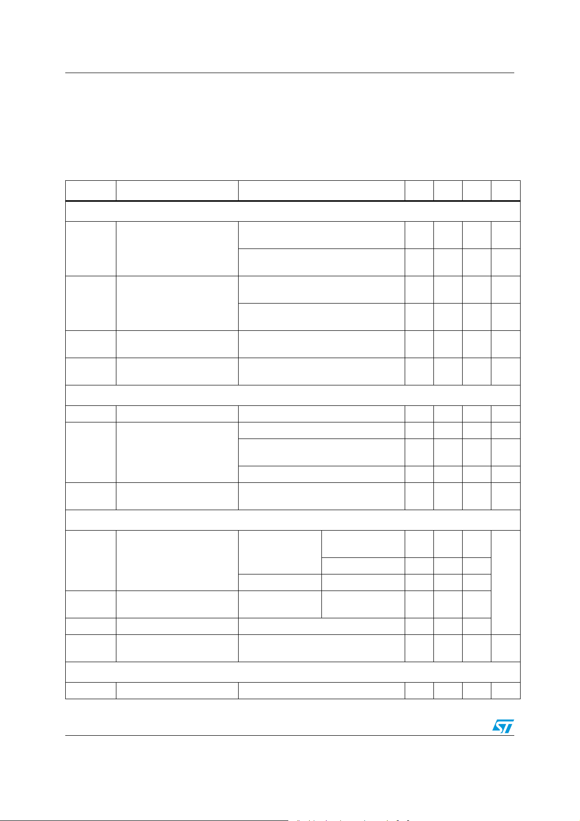
Table 6. Electrical characteristics (continued)
Symbol Parameter Test condition Min Typ Max Unit
Linear regulator and reference
LDO LDO output voltage
LDO_SW = GND, 5.5 V < VIN < 28 V,
LDOREFIN < 0.3 V, 0 < ILDO < 100 mA
LDO_SW = GND, 5.5 V < VIN < 28 V,
LDOREFIN = VREF3,
4.925 5.000 5.075 V
3.250 3.300 3.350 V
0 < ILDO < 100 mA
LDO accuracy in adjustable
mode
LDO short circuit current
(linear regulator enabled)
LDO_SW LDO_SW switch on threshold
LDO_SW LDO_SW hysteresis
VIN = 5.5 V to 28 V, LDOREFIN = 0.35 V
to 2.25 V, no load
-2.5 +2.5 %
LDO = 4.3 V, LDO_SW = GND 260 320 380 mA
LDO = 5 V, rising edge of LDO_SW,
LDOREFIN = GND
LDO = 5 V, falling edge of LDO_SW,
LDOREFIN = GND
4.64 4.75 4.84 V
200 400 mV
LDO = 5 V, rising edge of LDO_SW,
LDO_SW switch resistance
LDOREFIN = GND,
0.81 1.275 Ω
output current = 200 mA
VREF3 output voltage No load 3.235 3.300 3.365 V
VREF3
VREF3 current limit VREF3 = GND 22 30 mA
VREF2 VREF2 output voltage No load 1.980 2.000 2.02 V
VREF2 load regulation 0 < Load < 50 μA6mV
VREF2 sink current VREF2 > 2.030 V 10 µA
Fault management
VIN shutdown current EN1 and EN2 low, EN_LDO low 49 70 µA
VIN standby current
Operating power consumption
(VCC and VIN pins
consumption)
EN1 and EN2 low, EN_LDO high,
LDOREFIN = GND
Switching regulators on,
FB1 = SKIP = GND, REFIN2 = VCC,
LDOREFIN = GND,
OUT1 = LDO_SW = 5.3V, OUT2 = 3.5 V
132 180 µA
4,3 6,5 mW
Rising edge of PVCC 4.33 V
PVCC UVLO threshold
Falling edge of PVCC 4 V
Referred to FB1 nominal regulation point +11 %
Overvoltage trip threshold
Referred to REFIN2 nominal regulation
point. worst case:REFIN2 = 0.7 V
+14 %
PG threshold Lower threshold -13 -10 -7 %
PG low voltage ISink = 4 mA 159 235 405 mV
PG leakage current PG = 5 V 1 µA
Doc ID 15281 Rev 4 13/50
Electrical characteristics PM6686
Table 6. Electrical characteristics (continued)
Symbol Parameter Test condition Min Typ Max Unit
Output undervoltage
shutdown threshold
Inputs and outputs
FB1 FB1 logic level
REFIN2 REFIN2 logic level
LDOREFIN LDOREFIN logic level
SKIP SKIP logic level
TON TON logic level
EN1,2 EN level
Referred to FB1, REFIN2 nominal
regulation point
67 70 73 %
fixed OUT1 = 5 V 0.528 V
fixed OUT1 = 1.5 V 4.1 V
fixed OUT2 = 1.05 V, VCC = 5 V
fixed OUT 2= 3.3 V, VCC = 5 V
VREF3
VCC-
0.838
fixed LDO = 5 V 0.4 V
fixed LDO = 3.3 V 2.43 V
Pulse skip mode 0.8 V
No audible skip mode (VREF2 or floating)
VREF2 V
PWM mode 2.4 V
Low level 0.8 V
Middle level
VREF2
High level 2.4 V
Switching regulators off level 0.8 V
Delay start level
VREF2 V
Switching regulators on level 2.4 V
V
V
V
EN_LDO EN_LDO level
Input leakage current FB1 = 0.7 V -1 +1 µA
Internal bootstrap diode
Diode forward voltage PVCC = -BOOT, Idiode = 10 mA 0.2 V
Diode Leakage current BOOT= 30 V, PHASE = 28 V, PVCC = 5 V 500 nA
High-side and low-side gate drivers
HGATE driver on-resistance
LGATE driver on-resistance
Linear regulator off level 0.905 1.00 1.050 V
Linear regulator on level 1.500 1.6 1.650 V
REFIN2 = 2.5 V 12
HGATEx high state (pull-up)
Isource = 100 mA
HGATEx low state (pull-down)
Isink = 100 mA
LGATEx high state (pull-up)
Isource = 100 mA
LGATEx low state (pull-down)
Isink = 100 mA
1.8
1.3 1.9
1.3
0.6 0.8
Ω
14/50 Doc ID 15281 Rev 4
PM6686 Typical operating characteristics
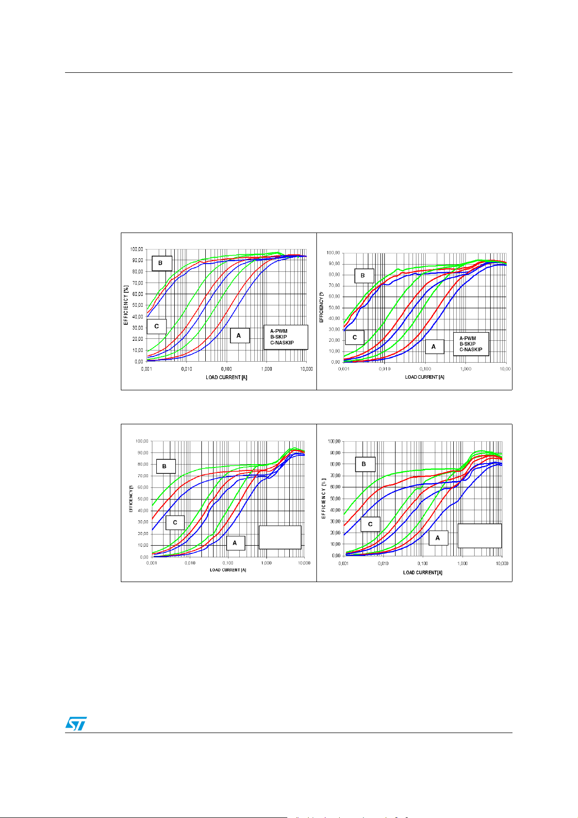
6 Typical operating characteristics
(TON = VCC (200 / 300 kHz), SKIP = GND (skip mode), LDOREFIN = SGND (LDO = 5 V),
LDO_SW = OUT1, PVCC connected to LDO, V
load unless specified). Measures performed on the demonstration kit (PM6686_SYSTEM
and PM6686_CHIPSET)
Efficiency traces: Green: VIN = 7 V, red: VIN = 12 V, blue: VIN = 19 V.
= 12 V, EN1-EN2-EN_LDO are high, no
IN
Figure 3. Efficiency vs load
OUT1 = 5 V, T
= VCC
ON
Figure 5. Efficiency vs load
OUT1 = 1.5 V, T
ON
= VCC
Figure 4. Efficiency vs load
OUT2 = 3.3 V, TON = VCC
Figure 6. Efficiency vs load
OUT2 = 1.05 V, TON = VCC
A-PWM
B-SKIP
A-NASKIP
A-PWM
B-SKIP
A-NASKIP
Doc ID 15281 Rev 4 15/50

Typical operating characteristics PM6686
Figure 7. Load regulation
OUT1 = 5 V, T
= VCC
ON
Figure 9. Load regulation
OUT1 = 1.5 V, T
= VCC
ON
Figure 8. Load regulation
OUT2 = 3.3 V, T
Figure 10. Load regulation
OUT2 = 1.05 V, TON = VCC
ON
= VCC
Figure 11. Switching frequency vs load
OUT1 = 5 V, T
16/50 Doc ID 15281 Rev 4
= VCC
ON
Figure 12. Switching frequency vs load
OUT2 = 3.3 V, TON = VCC

PM6686 Typical operating characteristics
Figure 13. Section 1 line regulation
OUT1 = 5 V, T
= VCC
ON
Figure 15. Section 1 line regulation
OUT1 = 1,5 V, T
ON
= VCC
Figure 14. Section 2 line regulation
OUT2 = 3.3 V, TON = VCC
Figure 16. Section 2 line regulation
OUT2 = 1,05 V, TON = VCC
Figure 17. Stand-by mode input battery
current vs input voltage
Figure 18. Shut-down mode input
battery current vs input
voltage
EN1=EN2=GND
FN_LDO=GND
Doc ID 15281 Rev 4 17/50

Typical operating characteristics PM6686
Figure 19. PWM no load input currents
vs input voltage
Figure 21. NA SKIP no load input
currents vs input voltage
Figure 20. SKIP no load input currents
vs input voltage
Figure 22. VREF3 load regulation
Figure 23. VREF2 load regulation Figure 24. LDO = 3.3 V load regulation
18/50 Doc ID 15281 Rev 4

PM6686 Typical operating characteristics
Figure 25. LDO = 5 V load regulation
6.1 Screen shots
Typical operating characteristic (T
= VCC (200 / 300 kHz), SKIP = GND (skip mode),
ON
FB1 = GND (OUT1 = 5 V), REFIN2 = VCC (OUT2 = 3.3 V), LDOREFIN = SGND
(LDO = 5 V), CP_FB = floating, LDO_SW = OUT1, PVCC connected to LDO, VIN = 12 V,
EN1-EN2-EN_LDO are high, no load unless specified)
Figure 26. OUT1 soft-start no load Figure 27. OUT2 soft-start no load
Doc ID 15281 Rev 4 19/50

Typical operating characteristics PM6686
Figure 28. OUT1 soft-start 8 A constant
Figure 30. OUT1 soft-end, no load Figure 31. OUT2 soft-end, no load
current load
Figure 29. OUT2 soft-start loaded 8 A
constant current load
Figure 32. OUT1 soft-start, EN2 = VREF2
20/50 Doc ID 15281 Rev 4
no loads applied
Figure 33. OUT2 soft-start, EN1=VREF2
no loads applied

PM6686 Typical operating characteristics
Figure 34. Soft-end, EN2 = VREF2 no
loads applied
Figure 36. Load transient 0-5 A 2 A/µs
OUT1 = 5 V PWM mode
Figure 35. Soft-end, EN1=VREF2 no
loads applied
Figure 37. Load transient 0-5 A 2 A/µs
OUT1 = 5 V SKIP mode
Figure 38. Load transient 0-5 A 2 A/ µs
OUT1 = 1.5 V PWM mode
Figure 39. Load transient 0-5 A 2 A/ µs
OUT1 = 1.5 V SKIP mode
Doc ID 15281 Rev 4 21/50

Typical operating characteristics PM6686
Figure 40. Load transient 0-5 A 2 A/µs
OUT2 = 3.3 V PWM mode
Figure 42. Load transient 0-5 A 2 A/ µs
OUT2 = 1.05 V PWM mode
Figure 41. Load transient 0-5 A 2 A/µs
OUT2 = 3.3 V SKIP mode
Figure 43. Load transient 0-5 A 2 A/ µs
OUT2 = 1.05 V SKIP mode
22/50 Doc ID 15281 Rev 4

PM6686 Block diagram
7 Block diagram
Figure 44. Functional block diagram
LD OR EFI N
LDO
LD O_ SW
CP_FB
BOOT1
HGAT E1
PHASE1
OU T1
UVLO
VREF3
+
-
VREF3 VREF2
VIN
VREF2
ADJ.
LIN EAR
REGUL ATOR
LDO EN INT
SWITCHOVER
+
THRE SH OLD
-
PVC C PVCC
LEVEL
SHIFTER
SM PS1
CONTROLLER
SMPS2
CONTROLLER
PVCC
LEV EL
SHIFTE R
PVCC
PVCC
VCC
ILIM1
ILIM2
BOOT2
HSIDE2
PHASE2
OU T2
LGA TE2
LGATE1
FB1
PG1
EN1
EN2
STARTUP
CONTROLLER
LDO EN INT
THER MAL
CONTROLLER
REFIN2
PG2
EN _LDO
TON SKIP
Doc ID 15281 Rev 4 23/50

Device description PM6686
8 Device description
The PM6686 is a dual step down controller dedicated to provide logic voltages for notebook
computers. It offers several operating configurations: it combines two synchronous buck
controllers, an internal linear regulator (LDO), two voltage references and a charge pump
controller.
Each buck controller is based on constant on time (COT) architecture. This type of control
offers a very fast load transient response with a minimum external components count.
The two switching sections (SMPS) generate two output voltages OUT1 and OUT2 that
regulate adjustable voltages. A fixed output voltage configuration can also be selected,
reducing further the external components count because no external resistor divider is
needed.
In fixed mode, OUT1 provides 5 V or 1.5 V; in adjustable mode OUT1 can regulate an output
voltage between 0.7 V and 5.5 V. In fixed mode, OUT2 provides 3.3 V or 1.05 V, in
adjustable mode OUT2 can regulate an output between 0.7 V to 2.5 V by tracking an
external reference.
The switching frequencies of both switching controllers can be adjusted to 200 kHz/300 kHz,
400 kHz/300 kHz or 400 kHz/500 kHz respectively. To maximize the efficiency at light loads
a pulse skipping mode can be selected. Moreover a pulse skipping mode with a minimum
switching frequency of 33 kHz (non audible skip operation mode) can be selected to avoid
audible noise issue. The linear regulator can provide a fixed (5 V or 3.3 V) or an adjustable
output voltage. In order to reduce the power consumption the internal LDO can be turned off
and the LDO output can be supplied with an external voltage applied at LDO_SW pin
(switch-over function).
The PM6686 supplies two voltage references: 3.3 V and 2 V. The charge pump controller
can be programmed to regulate a 14 V output. The switching sections and the LDO have
independent enable signals. Moreover the switching sections have a selectable power up
sequence and a turn off management.
The device is protected against overvoltage, undervoltage and over temperature. Two
independent Power Good signals monitor the output voltage range of each switching
sections.
8.1 Switching sections
8.1.1 Output voltage set up
The switching sections can be configured in several ways.
OUT1 output voltage is configured with FB1 pin. If FB1 pin is tied to GND the PM6686
regulates 5 V while if FB1 is connected to VCC the controller set OUT1 at 1.5 V. Using an
external resistor divider the output can be adjusted following this equation:
Equation 1
1R
⎛
V7,0V
1OUT
⎜
⎝
⎞
+⋅= 1
⎟
2R
⎠
24/50 Doc ID 15281 Rev 4

PM6686 Device description
Figure 45. Resistor divider to configure the output voltage
VOUT
CO UT
L
R1
PHASE
FB1
R2
Where R1, R2 are the resistors of the FB1 pin divider, as shown in Figure 2.
OUT2 output voltage is programmed with REFIN2 pin. Fixed output voltage is selected
connecting REFIN2 to VREF3 (OUT2 = 1.05 V) or to VCC (OUT2 = 3.3 V).
When the REFIN2 voltage is between 0.7 V and 2.5 V, OUT2 output voltage tracks REFIN2
voltage. When REFIN2 is lower than 0.5 V the section is turned OFF.
Table 7. Switching output voltages configuration
Output control pin
Control pin
connected to
Operation mode Output voltage
GND Fixed 5 V
VCC Fixed 1.5 V
OUT1 FB1
Resistor divider Adj
1R
⎛
V7.0V
1OUT
⎜
⎝
⎞
+⋅= 1
⎟
2R
⎠
VCC Fixed 3.3 V
OUT2 REFIN2
VREF3 Fixed 1.05 V
Ext source Tracking =REFIN2
Doc ID 15281 Rev 4 25/50

Device description PM6686
8.1.2 Constant on time control (COT)
PM6686 implements a pseudo-fixed frequency algorithm using the COT architecture. The
two sections are completely independent with separated switching controllers (SMPS).
The COT architecture bases its algorithm on the output ripple derived across the output
capacitor's ESR. The controller has an internal on time (T
output voltage valley: when VOUT reaches the regulation value a new T
duration is given by the following equation:
Equation 2
V
OUT
KT ⋅=
ON
V
IN
) generator triggered on the
ON
starts. The TON
ON
Where TON is the on time duration, K is a constant, V
is the sensed output voltage and
OUT
VIN is the input voltage.
The duty cycle in a buck converter is:
Equation 3
T
ON
T
SW
V
OUT
D
==
V
IN
The switching frequency in continuous current mode (CCM) is:
Equation 4
V
OUT
f
SW
D
T
ON
V
IN
==
V
OUT
⋅
K
V
1
=
K
IN
The switching frequency is theoretically constant, but in a real application it depends on
parasitic voltage drops that occur during the charging path (high-side switch resistance,
inductor resistance (DCR)) and discharging path (low-side switch resistance, DCR). As a
result the switching frequency increases as a function of the load current. The following
table shows the switching frequencies that can be selected through TON pin:
Table 8. Frequency configurations
SMPS 1 SMPS 2
TON
Frequency K Frequency K
VCC 200 kHz 5 µs 300 kHz 3.33 µs
VREF2 or open 400 kHz 2.5 µs 300 kHz 3.33 µs
26/50 Doc ID 15281 Rev 4
GND 400 kHz 2.5 µs 500 kHz 2 µs

PM6686 Device description
The COT architecture uses a minimum off-time (T
OFFMIN
) to allow inductor valley current
sense on the synchronous switch and to allow the charge of the bootstrap capacitor. A
minimum on-time is also introduced to assure the start-up sequence.
An adaptive anti-cross conduction algorithm avoids current paths between V
and GND
IN
during switching transition.
The PM6686 has three different operation modes selectable with SKIP pin: forced PWM
(PWM), pulse SKIP (SKIP) and non audible pulse SKIP (NA SKIP). The following
paragraphs explain in details the different features of these operation modes.
Table 9. Operative mode configurations
Control pin
SKIP
Control pin
connected to
Operation mode
VCC PWM
GND SKIP
VREF2 or floating NA SKIP
Figure 46. Constant on time block diagram
Toff min
BOOT
ILIM
OU T
VIN
1/10
PHA SE
Vol tag e
Reference
+
-
0,8V
-
+
PWM
Comparator
+
-
Z.C.
Comparator
-
SE T
Q
S
Q
R
CLR
Ton
ge ne ra tor
Level
Shifter
SE T
Q
S
Q
R
CLR
-
+
HS Driver
0,25V
-
-
+
-
PVCC
LS Driver
HGATE
PH ASE
0,5V
LGATE
PG ND
Doc ID 15281 Rev 4 27/50

Device description PM6686
f
t
8.1.3 PWM
PWM implements the continuous current mode (CCM). During TON, the high-side MOSFET
is turned on and the inductor current starts increasing. When the Ton is elapsed the highside MOSFET is turned off and after a dead time during which neither MOSFET conducts,
the low-side MOSFET turns on. The inductor current decreases until these three conditions
are verified:
● Output voltage reaches the regulation voltage
● Inductor current is below the current limit
● T
OFFMIN
When these conditions are satisfied a new T
PWM operation mode has a quasi-constant switching frequency, avoiding any audible noise
issue and the continuous current mode assures better load transitions despite of a lower
efficiency at light loads.
Figure 47. Inductor current and output voltage in PWM mode
Inductor
current
is elapsed
ON
starts.
Output
voltage
Vreg
Ton Tof
28/50 Doc ID 15281 Rev 4

PM6686 Device description
T
T
8.1.4 SKIP
To improve the efficiency at light load the PM6686 implements pulse skip operation mode.
When SKIP pin is tied to GND the inductor current is sensed and if it is equal to zero the
synchronous MOSFET is turned off. As a consequence the output capacitor is left floating
and the discharge depends only on the current sourced by the load. The new T
when the output reaches the voltage regulation. As a consequence at light load conditions
the switching frequency decreases improving the total efficiency of the converter. Working in
discontinuous current mode, the switching and the conduction losses are decreased
skipping some cycles.
If the output load is high enough to make the system work in CCM, skip mode is
automatically changed in PWM mode.
Figure 48. Inductor current and output voltage in SKIP mode
Inductor
current
Output
ON
starts
Vreg
ON
OFF
8.1.5 Non audible SKIP (NA SKIP)
To avoid audio noise the NA SKIP operation mode can be selected, connecting SKIP pin to
VREF2 or leaving it floating. In this condition if a new cycle doesn't start within 30
from the previous one the PM6686 turns on the low-side MOSFET to discharge the output
capacitor. The inductor current goes negative until the output reaches the voltage regulation
voltage allowing a new cycle to begin. If the switching frequency is above 33 kHz the device
works in SKIP mode.
This operation mode is useful to avoid audio noise but it lowers the efficiency at light loads if
it is compared to the SKIP mode.
μs typ.
Doc ID 15281 Rev 4 29/50

Device description PM6686
T
T
T
⋅⋅=
Figure 49. Inductor current and output voltage in NA SKIP mode
Inductor
cu rren t
Ou tput
Vreg
MA X
TON
OFF
IDLE
8.1.6 Gate drivers and logic supply
The integrated high-current drivers allow the use of different power MOSFET.
high-side driver is supplied with a bootstrap circuit with an integrated bootstrap diode. The
BOOT and the PHASE pins work respectively as supply and return rails for the HS driver.
The PVCC pin is the input for the supply of the low-side driver and PGND is the pin used as
return rail.
The PM6686 implements an anti-cross conduction protection which prevents high-side and
low-side MOSFET from being on at the same time.
The power dissipation of each driver can be calculated as:
Equation 5
Where V
The power dissipated by the drivers can be reduced lowering the sections switching
frequencies and mounting MOSFET with smaller Q
VCC pin is the input voltage rail to supply the internal logic circuit. This pin is connected
internally with a resistor to PVCC. As usual analog supply should be divided by the power
supply with a low pass filter to reduce the noise for the analog supply of the logic. Being the
resistor integrated it is enough to put a decoupling capacitor near VCC pin to realize the
filter with a components count reduction.
is the voltage applied to PVCC pin (+5 V) and fSW is the switching frequency.
PVCC
t
fQVP
swGPVCCDISS
.
G
30/50 Doc ID 15281 Rev 4

PM6686 Device description
Figure 50. Internal supply diagram
8.1.7 Current sensing and current limit
The PM6686 implements a positive valley current limit to protect the application from an
overcurrent fault. Each section has an independent current limit setting. A new switching
cycle can't start until the inductor current is under the positive current limit threshold. Note
that the peak current flowing in the inductor can reach a value greater than the current limit
threshold by an amount equal to the inductor ripple current.
Figure 51. Current waveforms in current limit conditions
The inductor current is sensed during the off time T
across the low-side MOSFET using the R
PGND voltage). The voltage drop is compared to the threshold set with ILIM pin. If ILIM is
connected to a voltage higher than VCC-1V the limit is 100mV. A current of 5 µA is sourced
from the pin ILIM; if a resistor is connected between ILIM and ground the current limit is
given by the voltage at the ILIM pin. The device sets the PHASE voltage threshold at 1/10 of
the ILIM voltage.
by measuring the voltage drop
OFF
as a lossless sensing element (PHASE to
DS(on)
Doc ID 15281 Rev 4 31/50

Device description PM6686
Figure 52. Current limit circuit block diagram
5uA
ILIM
RILIM
+
-
HGATE
9R
R
+-
Ton
Generator
PHASE
LGATE
Table 10. Current limit configuration
Control pin Control pin voltage Threshold SET
= VCC-1 V 100 mV
V
ILIM1
ILIM2
ILIM
0.2 V = V
V
= 5µA * R
ILIM
ILIM
= 2 V
ILIM
V
/10
ILIM
A negative current control is also implemented: the low-side MOSFET is forced off when the
current exceeds the negative limit. This function prevents the excessive negative inductor
current during the PWM operating mode. The threshold is set approximately at the 120% of
the positive current limit.
8.1.8 Soft-start and soft-end
The two sections have independent enable pins, EN1 and EN2. A not programmable softstart procedure takes place when EN pin rises above 2.4 V typ.
To prevent high input inrush currents, the current limit is increased from 25% to 100% with
steps of 25%.
The procedure is not programmable and ends typically in 2.8 ms. The overvoltage protection
is always active while the undervoltage protection is enabled typically 20 ms after the
beginning of the soft-start procedure.
Driving one EN pin below 0.8 V makes the section perform a soft-end: gate driving signals
32/50 Doc ID 15281 Rev 4
are pulled low and the output is discharged through an internal MOSFET with R
28
Ω typ.
A power up sequence for the switching sections can be selected connecting one EN pin to
VREF2.
DS(on)
of

PM6686 Device description
The section with the EN pin connected to VREF2 begins the soft-start only when the other
section is in regulation (its PGOOD is high) and makes a soft-end suddenly when the other
section is turned off.
Figure 53. VOUT2 behavior if EN2 is connected to VREF2
EN1
VOUT 1
PGO OD1
OUT 2
To protect the EN1, EN2, EN_LDO and SKIP pin of the PM6686 an external divider or a
series resistor is required, in order to prevent a large inrush current flowing into the device in
case the voltage spike is exceeding the recommended operating conditions.
Doc ID 15281 Rev 4 33/50

Monitoring and protections PM6686
9 Monitoring and protections
The PM6686 controls its switching output to prevent any damage or uncontrolled working
condition.
The device offers also PGOOD signals to monitor the state of each switching output voltage.
PGOOD is an open drain output: it is pulled low if the output voltage is below the 90% or
above the OVP threshold. of the nominal value.
9.1 Overvoltage protection
PM6686 provides a latched overvoltage protection (OVP). If the output voltage rises above
the +111% typ. for section 1 and above the +116% typ. for the section 2, a latched OVP
protection is activated. The controller tries to pull down the output voltage down to 0 V,
working in PWM. The current is limited by the negative current limit. The low-side MOSFET
is kept on when the output voltage is about 0 V. This management avoids high negative
undervoltage of the output rail that may damage the load.
The protection is latched and this fault is cleared toggling cleared by toggling EN or by
driving PVCC<3.979V and then PVCC>4.025V (PVCC Power On Reset).
9.2 Undervoltage protection
If during regulation the output voltage droops under the 70% of the nominal value, an
undervoltage latched fault is detected. The controller performs a soft-end procedure (see
“soft-start and soft-end” paragraph). The undervoltage fault is cleared by toggling EN or by
driving PVCC<3.979V and then PVCC>4.025V (PVCC power on reset).
9.3 PVCC monitor
The device monitors the driver supply voltage at PVCC pin. The switching sections can start
operating only if the voltage at PVCC pin is above 4,025 V typ. If PVCC falls below 3,979 V
typ., both the switching sections are turned off until the PVCC voltage goes over 4,025 V typ.
Table 11. Faults management summary
Fault Condition Device reaction
Overvoltage
section1
Overvoltage
section 2
Undervoltage V
PVCC
undervoltage
>+111%
V
OUT
>+116%
V
OUT
OUT
PVCC<3,979 V
<70%
Negative current limit protection activated. Low-side MOSFET is turned on when
the output voltage is about 0 V. Latched fault, cleared by toggling EN or by driving
PVCC<3.979V and then PVCC>4.025V (PVCC POR).
Negative current limit protection activated. Low-side MOSFET is turned on when
the output voltage is about 0 V. Latched fault, cleared by toggling EN or by driving
PVCC<3.979V and then PVCC>4.025V (PVCC POR).
The controller performs a soft-end. Latched fault cleared by toggling EN or by
driving PVCC<3.979V and then PVCC>4.025V (PVCC POR).
The controller turns off the switching sections. All faults of switching sections are
cleared. Not latched fault
34/50 Doc ID 15281 Rev 4

PM6686 Monitoring and protections
9.4 Linear regulator section
The PM6686 has an integrated linear regulator (LDO) that can provide an average of
100 mA typ. with a peak current of 270 mA typ. The LDO can be enabled using EN_LDO
pin. If VIN is applied the linear regulator is active even if PVCC is low.
The output voltage can be programmed by LDOREFIN pin. If LDOREFIN pin is tied to
ground (GND) the LDO provides a +5 V output voltage. If it is connected to VREF3 pin the
LDO regulates 3.3 V. If the voltage at the LDOREFIN pin is between 0.35 V and 2.25 V the
LDO generates an output voltage equals to 2xV
LDOREFIN
Table 12. LDO output voltage configuration
LDOREFIN voltage LDO voltage
GND +5 V
VREF3 +3,3 V
0,35 V < V
LDOREFIN
< 2,25 V 2x V
The controller provides a switchover function when LDOREFIN pin is connected to VCC or
GND. If the voltage at LDO_SW pin is high enough, the internal linear regulator is turned off
and the LDO pin is connected with an internal MOSFET to the LDO_SW pin. This feature
decreases the power dissipation of the device.
.
LDOREFIN
When the switchover function is used the maximum current capability is 200 mA if LDO
output is +5 V and 100 mA if the LDO output is +3.3 V.
Table 13. LDO switchover management
V
LDOREFIN
V
BYPLDO_SW
V
LDO
Internal LDO
< 0,35 V > 4,75 V +5 V Disabled 0.81 Ω
< 0,35 V < 4,55 V +5 V Enabled -
> 2.43 V > 3.18 V +3,3 V Disabled 1.12 Ω
> 2.43 V < 3.05 V +3,3 V Enabled -
0,35 V < V
LDOREFIN
< 2,25 V 2x V
LDOREFIN
Enabled -
Switchover
resistance
Doc ID 15281 Rev 4 35/50

Monitoring and protections PM6686
−+=
9.5 Charge pump
The PM6686 can drive an external charge pump circuit whose typical application schematic
is shown in the next figure.
Figure 54. Charge pump application circuit
COU T
Vout
L
D1
D2
D3
C2
CP
C4
D4
C1
C3
PHASE
LGAT E
R1
CP_F B
R2
The charge pump works in 4 phases:
1. LGATE is low. C1 is charged through the D1a diode at OUT1 voltage minus the diode
drop.
2. LGATE is driven high and C1 transfers the charge to C2. C2 voltage is OUT1 voltage
plus the LGATE voltage minus the voltage drops on D1 and D2.
3. LGATE is turned low and C2 shares its charge with C3 thought D3.
4. LGATE becomes high and C3 can charge C4 thought diode D4.
Every diode used to transfer charge introduces a voltage drop that decreases the charge
pump output voltage.
Repeating this cycle several times makes the charge pump output voltage equals to:
Equation 6
V4V2VV
DIODE1LGATE1OUTCP
Where VCP is the charge pump output voltage, V
section 1, V
LGATE1
is the low-side MOSFET gate driving voltage and V
is the output voltage of the switching
OUT1
is the forward
DIODE
voltage droop of the diodes used in the application.
CP_FB pin must be connected to the output of the charge pump with a resistor divider;
when CP_FB pin droops below 2 V typ., OUT1 controller starts a NA SKIP cycle to boost the
voltage of the charge pump.
36/50 Doc ID 15281 Rev 4

PM6686 Monitoring and protections
The minimum voltage of the charge pump is:
Equation 7
FB_CPMIN_CP
Where V
is the minimum voltage of CP_FB pin(2V typ.).
CP_FB
In case the charge pump feedback is not used, leave the CP_FB pin floating or connect the
pin to VCC.
9.6 Voltage references
The PM6686 provides two voltage references.
The device regulates a 3,3 V voltage reference (VREF3) with ±2% accuracy over
temperature. VREF3 can source up to 5 mA. VREF3 voltage is always available if V
applied. The device allows the enabling of the outputs if VREF3 is above 2,8V typ. and turns
off when VREF3 falls under 2,7 V typ.
VREF2 is a + 2 V reference with an accuracy of ±1% over temperature. It can source up to
50 µA typ. and sink up to 10 µA. VREF2is adopted as internal reference; this voltage can be
used as voltage threshold to set configuration pins (e.g. TON, SKIP pins). VREF2 is enabled
when one enable pin (EN1, EN2 or EN_LDO) is pulled high.
9.7 General device fault management
⎛
⎜
⎜
⎝
⎞
R
1
⎟
1VV
+⋅=
⎟
R
2
⎠
is
IN
9.7.1 Thermal protection
If the internal temperature of the device exceeds typically +150 °C, the controller shuts down
immediately all the internal circuitry. Switching sections performs the soft-end management.
Toggling EN, EN LDO or cycling VIN resets the latched fault.
Doc ID 15281 Rev 4 37/50

Application information PM6686
10 Application information
10.1 External components selection
10.1.1 Inductor
Once that switching frequency is defined, inductor selection depends on the desired
inductor ripple current and load transient performance.
Low inductance means great ripple current and could generate great output noise. On the
other hand, low inductor values involve fast load transient response.
A good compromise between the transient response time, the efficiency, the cost and the
size is to choose the inductor value in order to maintain the inductor ripple current
between 20% and 50% of the maximum output current ILOAD (max). The maximum
occurs at the maximum input voltage. With these considerations, the inductor value can be
calculated with the following relationship:
Equation 8
ΔI
L
ΔI
L
VV
L
−
=
Δ×
Where fSW is the switching frequency, VIN is the input voltage, V
and
ΔI
is the selected inductor ripple current.
L
V
OUTIN
OUT
×
V
If
Lsw
IN
is the output voltage
OUT
In order to prevent overtemperature working conditions, inductor must be able to provide an
RMS current greater than the maximum RMS inductor current I
LRMS
:
Equation 9
(max))I(I
LOADLRMS
L
+=
12
2
(max))I(
Δ
2
Where ΔIL(max) is the maximum ripple current:
Equation 10
VV
−
sw
OUTmaxIN
Lf
×
(max)I ×
L
=Δ
V
OUT
V
maxIN
If hard saturation inductors are used, the inductor saturation current should be much greater
than the maximum inductor peak current Ipeak:
Equation 11
Using soft-saturation inductors it’s possible to choose inductors with saturation current limit
nearly to Ipeak.
Below there is a list of some inductor manufacturers.
38/50 Doc ID 15281 Rev 4
LOAD
(max)I
Δ
(max)IIpeak
L
+=
2

PM6686 Application information
Δ×=
Table 14. Inductor manufacturer
Manufacturer Series Inductor value (µH) RMS current (A) Saturation current (A)
COILCRAFT MSS-1048 3,3 7,22 7,6
COILCRAFT MSS-1260 3,3 9,7 7
COILCRAFT MLC-1550 2,5 16,5 11,4
10.1.2 Input capacitor
In a buck topology converter the current that flows into the input capacitor is a pulsed current
with zero average value. The input RMS current of the two switching sections can be roughly
estimated as follows:
Equation 12
Where D1, D2 are the duty cycles and I1, I2 are the maximum load currents of the two
sections.
Input capacitor should be chosen with an RMS rated current higher than the maximum RMS
current given by both sections.
Tantalum capacitors are good in term of low ESR and small size, but they occasionally can
burn out if subjected to very high current during the charge. Ceramic capacitors have
usually a higher RMS current rating with smaller size and they remain the best choice.
Below there is a list of some ceramic capacitor manufacturers.
Table 15. Input capacitor manufacturer
Manufacturer Series Capacitor value (µF) Rated voltage (V)
TAYIO YUDEN UMK325BJ106 KM-T 10 50
TAYIO YUDEN GMK325BJ106MN 10 35
10.1.3 Output capacitor
The selection of the output capacitor is based on the ESR value and on the voltage rating
rather than on the capacitor value Cout.
2
11CinRMS
2
221
)D1(ID)D1(IDI
−××+−××=
2
The output capacitor has to satisfy the output voltage ripple requirements. Lower inductor
value can reduce the size of the choke but increases the inductor current ripp
Since the voltage ripple V
RIPPLEout
is given by:
le ΔIL.
Equation 13
IRV
LoutRIPPLEout
A low ESR capacitor is required to reduce the output voltage ripple. Switching sections can
work correctly even with 15mV output ripple.
Doc ID 15281 Rev 4 39/50

Application information PM6686
Δ
Finally the output capacitor choice deeply impacts on the load transient response. Below
there is a list of some capacitor manufacturers.
Output capacitor manufacturer
Table 16. Input capacitor manufacturer
Manufacturer Series Capacitor value (µF) Rated voltage (V) ESR max (mΩ)
SANYO POSCAP TPB 150 to 330 2.5 to 6.3 35 to 65
SANYO POSCAP TPF 150 to 470 2.5 to 6.3 7 to 15
10.1.4 MOSFET
Logic-level MOSFETs are recommended, since low-side and high-side gate drivers are
powered by PVCC. Their breakdown voltage (VBRDSS) must be higher than the maximum
input voltage.
In notebook applications, power management efficiency is a high level requirement. The
power dissipation on the power switches becomes an important factor in switching
selections. Losses of high-side and low-side MOSFETs depend on their working conditions.
The power dissipation of the high-side MOSFET is given by:
Equation 14
PPP +=
switchingconductionDHighSide
Maximum conduction losses are approximately:
Equation 15
Where R
V
RP ××=
DSonconduction
is the drain-source on resistance of the high-side MOSFET.
DS(on)
OUT
V
LOAD
minIN
2
(max)I
Switching losses are approximately:
Equation 16
Δ
I
L
+×
2
××
ft)
swoff
2
P
switching
Where ton and t
I
=
LOADIN
are the switching times of the turn off and turn off phases of the
off
2
2
L
−×
(max)I(V
××
ft)
(max)I(V
LOADINswon
+
MOSFETs.
As general rule, high-side MOSFETs with low gate charge are recommended, in order to
minimize driver losses.
Below there is a list of possible choices for the high-side MOSFETs.
40/50 Doc ID 15281 Rev 4

PM6686 Application information
=
Table 17. High-side MOSFET manufacturer
Manufacturer Type Gate charge (nC) R
(mΩ) Rated reverse voltage (V)
DS(on)
ST STS12NH3LL 10 8 30
ST STS17NH3LL 18 4 30
The power dissipation of the low-side MOSFET is given by:
Equation 17
PP
conductionDLowSide
Maximum conduction losses occur at the maximum input voltage:
Equation 18
DSonconduction
Choose a synchronous rectifier with low R
⎛
⎜
1RP ×
−×=
⎜
V
⎝
DS(on)
⎞
V
OUT
maxIN
⎟
LOAD
⎟
⎠
2
(max)I
. When high-side MOSFET turns on, the
fast variation of the phase node voltage can bring up even the low-side gate through its
gate-drain capacitance CRSS, causing cross-conduction problems. Choose a low-side
MOSFETs that minimizes the ratio CRSS/CGS (CGS = CISS - CRSS).
Below there is a list of some possible low-side MOSFETs.
Table 18. Low-side MOSFET manufacturer
C
Manufacturer Type R
DS(on)
(mΩ)
C
RSS
GS
ST STS17NF3LL 5.5 0.047 30
ST STS25NH3LL 3.5 0.011 30
Rated reverse voltage
(V)
Dual N-channel MOSFETs can be used in applications with a maximum output current of
about 3 A. Below there is a list of some MOSFETs manufacturers.
Table 19. Dual MOSFET manufacturer
Manufacturer Type R
DS(on)
(mΩ)
Gate charge
(nC)
ST STS8DNH3LL 25 10 30
ST STS4DNF60L 65 32 60
Rated reverse voltage
(V)
Doc ID 15281 Rev 4 41/50

Diode selection PM6686
11 Diode selection
11.1 Freewheeling diode
A rectifier across the low-side MOSFET is recommended. The rectifier works as a voltage
clamp across the synchronous rectifier and reduces the negative inductor swing during the
dead time between turning the high-side MOSFET off and the synchronous rectifier on. It
can increase the efficiency of the switching section, since it reduces the low-side switch
losses. A Schottky diode is suitable for its low forward voltage drop (0.3 V). The diode
reverse voltage must be greater than the maximum input voltage. A minimum recovery
reverse charge is preferable. Below there is a list of some Schottky diode manufacturers.
Table 20. Schottky diode manufacturer
Manufacturer Series
ST STPS1L30M 0.34 30 0.00039
ST STPS1L20M 0.37 20 0.000075
11.2 Charge pump diode
The charge pump capacitors are fed by the current supplied by LGATE1 (output of the lowside driver for the section 1). Dual in package diodes, in series configuration, could be used
to reduce the area occupation.
Table 21. Schottky diode manufacturer
Manufacturer Series
ST BAT54S 0.24 40 0.3
ST BAR43A 0.35 30 0.1
ST BAS69-04 0.35 15 0.01
Forward voltage
(V)
Forward voltage
(V)
Rated reverse
voltage (V)
Rated reverse
voltage (V)
Reverse current
(μA)
Max forward
current (A)
42/50 Doc ID 15281 Rev 4

PM6686 Diode selection
11.3 Other important components
11.3.1 VIN filter
A VIN pin low pass filter is suggested to reduce switching noise. The low pass filter is shown
in the next figure:
Figure 55. VIN pin filter
Typical component value is: C = 1 µF.
11.3.2 PVCC and VCC
PVCC and VCC are connected with an internal resistor (about 10 Ω); this allows reducing
the external components. Connect the +5 V supply rail only to PVCC.
Use a bypass capacitor on PVCC pin. A VCC low pass filter helps to reject switching
commutations noise, this filter can be implemented simply adding a bypass capacitor on
VCC pin.
Figure 56. VCC and PVCC filters
Input
Voltage
VIN
C
C2
PVCC
C1
VC C
Doc ID 15281 Rev 4 43/50

Diode selection PM6686
Typical components values are: C1 = 1 µF and C2 = 1 µF.
11.3.3 VREF2 and VREF3 capacitors
A 10 nF to 100 nF ceramic capacitor on VREF2 pin must be added to ensure noise
rejection. If VREF3 voltage is not used the pin can be left floating, otherwise a 10 nF to 100
nF bypass ceramic capacitor should be mounted.
11.3.4 LDO output capacitors
Bypass the output of the linear regulator with 4,7 µF ceramic capacitor closer to the LDO
pin. In most applicative conditions the ceramic output capacitor can be enough to ensure
stability.
11.3.5 Bootstrap circuit
The external bootstrap circuit is represented in the next figure:
Figure 57. Bootstrap circuit
RBOOT
RBOOT
CBOOT
PHASE
L
The bootstrap circuit capacitor value CBOOT must provide the total gate charge to the highside MOSFET during turn on phase. A typical value is 100 nF.
A resistor RBOOT on the BOOT pin could be added in order to reduce noise when the
phase node rises up, working like a gate resistor for the turn on phase of the high-side
MOSFET. A typical value is R
BOOT
= 1 Ω.
44/50 Doc ID 15281 Rev 4

PM6686 PCB design guidelines
12 PCB design guidelines
The layout is very important in terms of efficiency, stability and noise of the system. It is
possible to refer to the PM6686 demonstration board for a complete layout example.
For good PC board layout follows these guidelines:
● Place on the top side all the power components (inductors, input and output capacitors,
MOSFETs and diodes). Refer them to a power ground plan, PGND. If possible, reserve
a layer to PGND plan. The PGND plan is the same for both the switching sections.
● AC current paths layout is very critical (see Figure 58). The first priority is to minimize
their length. Trace the LS MOSFET connection to PGND plan as short as possible.
Place the synchronous diode D near the LS MOSFET. Connect the LS MOSFET drain
to the switching node with a short trace.
● Place input capacitors near HS MOSFET drain. It is recommended to use the same
input voltage plan for both the switching sections, in order to put together all input
capacitors.
● Place all the sensitive analog signals (feedbacks, voltage references, current sense
paths) on the bottom side of the board or in an inner layer. Isolate them from the power
top side with a signal ground layer, SGND. Connect the SGND and PGND plans only in
one point (a multiple vias connection is preferable to a 0 Ω resistor connection) near the
PGND device pin. Place the device on the top or on the bottom size and connect the
exposed pad and the SGND pins to the SGND plan (see
● As general rule, make the high-side and low-side drivers traces wide and short.
● The high-side driver is powered by the bootstrap circuit. It’s very important to place
capacitor CBOOT as near as possible to the BOOT pin (for example on the layer
opposite to the device). Route HGATE and PHASE traces as near as possible in order
to minimize the area between them.
● The low-side gate driver is powered by PVCC pin. Placing PGND and LGATE pins near
the low-side MOSFETs reduces the length of the traces and the crosstalk noise
between the two sections.
● The linear regulator outputs are referred to SGND as long as the reference voltages
VREF2 and VREF3. Place their output filtering capacitors as near as possible to the
device.
● Place input filtering capacitors near PVCC, VCC and VIN pins.
Figure 58).
Doc ID 15281 Rev 4 45/50

PCB design guidelines PM6686
Figure 58. Current paths, ground connection and driver traces layout
46/50 Doc ID 15281 Rev 4

PM6686 Package mechanical data
13 Package mechanical data
In order to meet environmental requirements, ST offers these devices in different grades of
ECOPACK
®
packages, depending on their level of environmental compliance. ECOPACK®
specifications, grade definitions and product status are available at: www.st.com.
ECOPACK is an ST trademark.
Table 22. VFQFPN 5x5x1.0 mm 32 L pitch 0.50 mechanical data
Databook (mm)
Dim.
Min Typ Max
A0.80.91
A1 0 0.02 0.05
A3 0.2
b 0.18 0.25 0.3
D4.8555.15
D2 See exposed pad variations
E4.8555.15
E2 See exposed pad variations
e0.5
L 0.3 0.4 0.5
ddd 0.05
(2)
(2)
Table 23. Exposed pad variations
(1)(2)
D2
E2
Min Typ Max Min Typ Max
2.90 3.10 3.20 2.90 3.10 3.20
1. VFQFPN stands for thermally enhanced very thin fine pitch quad flat package no lead. Very thin:
A = 1.00 mm max.
2. Dimensions D2 and E2 are not in accordance with JEDEC.
Doc ID 15281 Rev 4 47/50

Package mechanical data PM6686
Figure 59. Package dimensions
48/50 Doc ID 15281 Rev 4

PM6686 Revision history
14 Revision history
Table 24. Document revision history
Date Revision Changes
09-Jan-2009 1 Initial release
26-Feb-2009 2 Updated input voltage range in coverpage
07-May-2009 3 Updated pin 29 description in Table 2 on page 7
23-Jul-2009 4
Updated Table 3 on page 10, Section 8.1.8 on page 32, Section 9.1
on page 34, Section 9.2 on page 34 and Table 11 on page 34
Doc ID 15281 Rev 4 49/50

PM6686
Please Read Carefully:
Information in this document is provided solely in connection with ST products. STMicroelectronics NV and its subsidiaries (“ST”) reserve the
right to make changes, corrections, modifications or improvements, to this document, and the products and services described herein at any
time, without notice.
All ST products are sold pursuant to ST’s terms and conditions of sale.
Purchasers are solely responsible for the choice, selection and use of the ST products and services described herein, and ST assumes no
liability whatsoever relating to the choice, selection or use of the ST products and services described herein.
No license, express or implied, by estoppel or otherwise, to any intellectual property rights is granted under this document. If any part of this
document refers to any third party products or services it shall not be deemed a license grant by ST for the use of such third party products
or services, or any intellectual property contained therein or considered as a warranty covering the use in any manner whatsoever of such
third party products or services or any intellectual property contained therein.
UNLESS OTHERWISE SET FORTH IN ST’S TERMS AND CONDITIONS OF SALE ST DISCLAIMS ANY EXPRESS OR IMPLIED
WARRANTY WITH RESPECT TO THE USE AND/OR SALE OF ST PRODUCTS INCLUDING WITHOUT LIMITATION IMPLIED
WARRANTIES OF MERCHANTABILITY, FITNESS FOR A PARTICULAR PURPOSE (AND THEIR EQUIVALENTS UNDER THE LAWS
OF ANY JURISDICTION), OR INFRINGEMENT OF ANY PATENT, COPYRIGHT OR OTHER INTELLECTUAL PROPERTY RIGHT.
UNLESS EXPRESSLY APPROVED IN WRITING BY AN AUTHORIZED ST REPRESENTATIVE, ST PRODUCTS ARE NOT
RECOMMENDED, AUTHORIZED OR WARRANTED FOR USE IN MILITARY, AIR CRAFT, SPACE, LIFE SAVING, OR LIFE SUSTAINING
APPLICATIONS, NOR IN PRODUCTS OR SYSTEMS WHERE FAILURE OR MALFUNCTION MAY RESULT IN PERSONAL INJURY,
DEATH, OR SEVERE PROPERTY OR ENVIRONMENTAL DAMAGE. ST PRODUCTS WHICH ARE NOT SPECIFIED AS "AUTOMOTIVE
GRADE" MAY ONLY BE USED IN AUTOMOTIVE APPLICATIONS AT USER’S OWN RISK.
Resale of ST products with provisions different from the statements and/or technical features set forth in this document shall immediately void
any warranty granted by ST for the ST product or service described herein and shall not create or extend in any manner whatsoever, any
liability of ST.
ST and the ST logo are trademarks or registered trademarks of ST in various countries.
Information in this document supersedes and replaces all information previously supplied.
The ST logo is a registered trademark of STMicroelectronics. All other names are the property of their respective owners.
© 2009 STMicroelectronics - All rights reserved
Australia - Belgium - Brazil - Canada - China - Czech Republic - Finland - France - Germany - Hong Kong - India - Israel - Italy - Japan -
STMicroelectronics group of companies
Malaysia - Malta - Morocco - Philippines - Singapore - Spain - Sweden - Switzerland - United Kingdom - United States of America
www.st.com
50/50 Doc ID 15281 Rev 4
 Loading...