

Page 1

PM0044
Programming manual
STM8 CPU programming manual
Introduction
The STM8 family of HCMOS microcontrollers is designed and built around an enhanced
industry standard 8-bit core and a library of peripheral blocks, which include ROM, Flash,
RAM, EEPROM, I/O, Serial Interfaces (SPI, USART, I2C,...), 16-bit Timers, A/D converters,
comparators, power supervisors etc. These blocks may be assembled in various
combinations in order to provide cost-effective solutions for application-specific products.
The STM8 family forms a part of the STMicroelectronics 8-bit MCU product line, which finds
its place in a wide variety of applications such as automotive systems, remote controls,
video monitors, car radio and numerous other consumer, industrial, telecom, and multimedia
products.
September 2011 Doc ID 13590 Rev 3 1/162
www.st.com
Page 2

Contents PM0044
Contents
1 STM8 architecture . . . . . . . . . . . . . . . . . . . . . . . . . . . . . . . . . . . . . . . . . . . 9
1.1 STM8 development support . . . . . . . . . . . . . . . . . . . . . . . . . . . . . . . . . . . 10
1.2 Enhanced STM8 features . . . . . . . . . . . . . . . . . . . . . . . . . . . . . . . . . . . . . 11
2 Glossary . . . . . . . . . . . . . . . . . . . . . . . . . . . . . . . . . . . . . . . . . . . . . . . . . . 12
3 STM8 core description . . . . . . . . . . . . . . . . . . . . . . . . . . . . . . . . . . . . . . 13
3.1 Introduction . . . . . . . . . . . . . . . . . . . . . . . . . . . . . . . . . . . . . . . . . . . . . . . 13
3.2 CPU registers . . . . . . . . . . . . . . . . . . . . . . . . . . . . . . . . . . . . . . . . . . . . . . 13
4 STM8 memory interface . . . . . . . . . . . . . . . . . . . . . . . . . . . . . . . . . . . . . 17
4.1 Program space . . . . . . . . . . . . . . . . . . . . . . . . . . . . . . . . . . . . . . . . . . . . . 17
4.2 Data space . . . . . . . . . . . . . . . . . . . . . . . . . . . . . . . . . . . . . . . . . . . . . . . . 17
4.3 Memory interface architecture . . . . . . . . . . . . . . . . . . . . . . . . . . . . . . . . . 19
5 Pipelined execution . . . . . . . . . . . . . . . . . . . . . . . . . . . . . . . . . . . . . . . . . 20
5.1 Description of pipelined execution stages . . . . . . . . . . . . . . . . . . . . . . . . 20
5.1.1 Fetch stage . . . . . . . . . . . . . . . . . . . . . . . . . . . . . . . . . . . . . . . . . . . . . . 21
5.1.2 Decoding and addressing stage . . . . . . . . . . . . . . . . . . . . . . . . . . . . . . 21
5.1.3 Execution stage . . . . . . . . . . . . . . . . . . . . . . . . . . . . . . . . . . . . . . . . . . . 22
5.2 Data memory conflicts . . . . . . . . . . . . . . . . . . . . . . . . . . . . . . . . . . . . . . . 22
5.3 Pipelined execution examples . . . . . . . . . . . . . . . . . . . . . . . . . . . . . . . . . 23
5.4 Conventions . . . . . . . . . . . . . . . . . . . . . . . . . . . . . . . . . . . . . . . . . . . . . . . 23
5.4.1 Optimized pipeline example – execution from Flash Program memory . 24
5.4.2 Optimize pipeline example – execution from RAM . . . . . . . . . . . . . . . . 26
5.4.3 Pipeline with Call/Jump . . . . . . . . . . . . . . . . . . . . . . . . . . . . . . . . . . . . . 27
5.4.4 Pipeline stalled . . . . . . . . . . . . . . . . . . . . . . . . . . . . . . . . . . . . . . . . . . . . 27
5.4.5 Pipeline with 1 wait state . . . . . . . . . . . . . . . . . . . . . . . . . . . . . . . . . . . . 29
6 STM8 addressing modes . . . . . . . . . . . . . . . . . . . . . . . . . . . . . . . . . . . . 30
6.1 Inherent addressing mode . . . . . . . . . . . . . . . . . . . . . . . . . . . . . . . . . . . . 32
6.2 Immediate addressing mode . . . . . . . . . . . . . . . . . . . . . . . . . . . . . . . . . . 33
6.3 Direct addressing mode (Short, Long, Extended) . . . . . . . . . . . . . . . . . . 34
2/162 Doc ID 13590 Rev 3
Page 3

PM0044 Contents
6.3.1 Short Direct addressing mode . . . . . . . . . . . . . . . . . . . . . . . . . . . . . . . . 36
6.3.2 Long Direct addressing mode . . . . . . . . . . . . . . . . . . . . . . . . . . . . . . . . 37
6.3.3 Extended Direct addressing mode (only for CALLF and JPF) . . . . . . . . 38
6.4 Indexed addressing mode (No Offset, Short, SP, Long, Extended) . . . . . 39
6.4.1 No Offset Indexed addressing mode . . . . . . . . . . . . . . . . . . . . . . . . . . . 40
6.4.2 Short Indexed addressing mode . . . . . . . . . . . . . . . . . . . . . . . . . . . . . . 41
6.4.3 SP Indexed addressing mode . . . . . . . . . . . . . . . . . . . . . . . . . . . . . . . . 42
6.4.4 Long Indexed addressing mode . . . . . . . . . . . . . . . . . . . . . . . . . . . . . . . 43
6.4.5 Extended Indexed (only LDF instruction) . . . . . . . . . . . . . . . . . . . . . . . . 44
6.5 Indirect (Short Pointer Long, Long Pointer Long) . . . . . . . . . . . . . . . . . . . 45
6.6 Short Pointer Indirect Long addressing mode . . . . . . . . . . . . . . . . . . . . . 46
6.7 Long Pointer Indirect Long addressing mode . . . . . . . . . . . . . . . . . . . . . . 47
6.8 Indirect Indexed (Short Pointer Long, Long Pointer Long,
Long Pointer Extended) addressing mode . . . . . . . . . . . . . . . . . . . . . . . . 48
6.9 Short Pointer Indirect Long Indexed addressing mode . . . . . . . . . . . . . . 49
6.10 Long Pointer Indirect Long Indexed addressing mode . . . . . . . . . . . . . . . 51
6.11 Long Pointer Indirect Extended Indexed addressing mode . . . . . . . . . . . 53
6.12 Relative Direct addressing mode . . . . . . . . . . . . . . . . . . . . . . . . . . . . . . . 55
6.13 Bit Direct (Long) addressing mode . . . . . . . . . . . . . . . . . . . . . . . . . . . . . . 57
6.14 Bit Direct (Long) Relative addressing mode . . . . . . . . . . . . . . . . . . . . . . . 59
7 STM8 instruction set . . . . . . . . . . . . . . . . . . . . . . . . . . . . . . . . . . . . . . . . 61
7.1 Introduction . . . . . . . . . . . . . . . . . . . . . . . . . . . . . . . . . . . . . . . . . . . . . . . 61
7.2 Nomenclature . . . . . . . . . . . . . . . . . . . . . . . . . . . . . . . . . . . . . . . . . . . . . . 63
7.2.1 Operators . . . . . . . . . . . . . . . . . . . . . . . . . . . . . . . . . . . . . . . . . . . . . . . . 63
7.2.2 CPU registers . . . . . . . . . . . . . . . . . . . . . . . . . . . . . . . . . . . . . . . . . . . . 63
7.2.3 Code condition bit value notation . . . . . . . . . . . . . . . . . . . . . . . . . . . . . . 63
7.2.4 Memory and addressing . . . . . . . . . . . . . . . . . . . . . . . . . . . . . . . . . . . . 63
7.2.5 Operation code notation . . . . . . . . . . . . . . . . . . . . . . . . . . . . . . . . . . . . 64
7.3 Instruction set summary . . . . . . . . . . . . . . . . . . . . . . . . . . . . . . . . . . . . . . 64
7.4 Instruction set . . . . . . . . . . . . . . . . . . . . . . . . . . . . . . . . . . . . . . . . . . . . . . 74
ADC . . . . . . . . . . . . . . . . . . . . . . . . . . . . . . . . . . . . . . . . . . . . . . . . . . . . . . . . . . . 75
ADD . . . . . . . . . . . . . . . . . . . . . . . . . . . . . . . . . . . . . . . . . . . . . . . . . . . . . . . . . . . 77
ADDW. . . . . . . . . . . . . . . . . . . . . . . . . . . . . . . . . . . . . . . . . . . . . . . . . . . . . . . . . . 78
AND . . . . . . . . . . . . . . . . . . . . . . . . . . . . . . . . . . . . . . . . . . . . . . . . . . . . . . . . . . . 79
Doc ID 13590 Rev 3 3/162
Page 4

Contents PM0044
BCCM . . . . . . . . . . . . . . . . . . . . . . . . . . . . . . . . . . . . . . . . . . . . . . . . . . . . . . . . . . 80
BCP . . . . . . . . . . . . . . . . . . . . . . . . . . . . . . . . . . . . . . . . . . . . . . . . . . . . . . . . . . . 81
BCPL . . . . . . . . . . . . . . . . . . . . . . . . . . . . . . . . . . . . . . . . . . . . . . . . . . . . . . . . . . 82
BREAK . . . . . . . . . . . . . . . . . . . . . . . . . . . . . . . . . . . . . . . . . . . . . . . . . . . . . . . . . 83
BRES . . . . . . . . . . . . . . . . . . . . . . . . . . . . . . . . . . . . . . . . . . . . . . . . . . . . . . . . . . 84
BSET . . . . . . . . . . . . . . . . . . . . . . . . . . . . . . . . . . . . . . . . . . . . . . . . . . . . . . . . . . 85
BTJF . . . . . . . . . . . . . . . . . . . . . . . . . . . . . . . . . . . . . . . . . . . . . . . . . . . . . . . . . . . 86
BTJT . . . . . . . . . . . . . . . . . . . . . . . . . . . . . . . . . . . . . . . . . . . . . . . . . . . . . . . . . . . 87
CALL. . . . . . . . . . . . . . . . . . . . . . . . . . . . . . . . . . . . . . . . . . . . . . . . . . . . . . . . . . . 88
CALLF. . . . . . . . . . . . . . . . . . . . . . . . . . . . . . . . . . . . . . . . . . . . . . . . . . . . . . . . . . 89
CALLR . . . . . . . . . . . . . . . . . . . . . . . . . . . . . . . . . . . . . . . . . . . . . . . . . . . . . . . . . 90
CCF. . . . . . . . . . . . . . . . . . . . . . . . . . . . . . . . . . . . . . . . . . . . . . . . . . . . . . . . . . . . 91
CLR. . . . . . . . . . . . . . . . . . . . . . . . . . . . . . . . . . . . . . . . . . . . . . . . . . . . . . . . . . . . 92
CLRW . . . . . . . . . . . . . . . . . . . . . . . . . . . . . . . . . . . . . . . . . . . . . . . . . . . . . . . . . . 93
CP. . . . . . . . . . . . . . . . . . . . . . . . . . . . . . . . . . . . . . . . . . . . . . . . . . . . . . . . . . . . . 94
CPW . . . . . . . . . . . . . . . . . . . . . . . . . . . . . . . . . . . . . . . . . . . . . . . . . . . . . . . . . . . 95
CPL. . . . . . . . . . . . . . . . . . . . . . . . . . . . . . . . . . . . . . . . . . . . . . . . . . . . . . . . . . . . 97
CPLW . . . . . . . . . . . . . . . . . . . . . . . . . . . . . . . . . . . . . . . . . . . . . . . . . . . . . . . . . . 98
DEC . . . . . . . . . . . . . . . . . . . . . . . . . . . . . . . . . . . . . . . . . . . . . . . . . . . . . . . . . . . 99
DECW. . . . . . . . . . . . . . . . . . . . . . . . . . . . . . . . . . . . . . . . . . . . . . . . . . . . . . . . . 100
DIV . . . . . . . . . . . . . . . . . . . . . . . . . . . . . . . . . . . . . . . . . . . . . . . . . . . . . . . . . . . 101
DIVW. . . . . . . . . . . . . . . . . . . . . . . . . . . . . . . . . . . . . . . . . . . . . . . . . . . . . . . . . . 102
EXG . . . . . . . . . . . . . . . . . . . . . . . . . . . . . . . . . . . . . . . . . . . . . . . . . . . . . . . . . . 103
EXGW. . . . . . . . . . . . . . . . . . . . . . . . . . . . . . . . . . . . . . . . . . . . . . . . . . . . . . . . . 104
HALT. . . . . . . . . . . . . . . . . . . . . . . . . . . . . . . . . . . . . . . . . . . . . . . . . . . . . . . . . . 105
INC . . . . . . . . . . . . . . . . . . . . . . . . . . . . . . . . . . . . . . . . . . . . . . . . . . . . . . . . . . . 106
INCW . . . . . . . . . . . . . . . . . . . . . . . . . . . . . . . . . . . . . . . . . . . . . . . . . . . . . . . . . 107
INT . . . . . . . . . . . . . . . . . . . . . . . . . . . . . . . . . . . . . . . . . . . . . . . . . . . . . . . . . . . 108
IRET . . . . . . . . . . . . . . . . . . . . . . . . . . . . . . . . . . . . . . . . . . . . . . . . . . . . . . . . . . 109
JP . . . . . . . . . . . . . . . . . . . . . . . . . . . . . . . . . . . . . . . . . . . . . . . . . . . . . . . . . . . . 110
JPF . . . . . . . . . . . . . . . . . . . . . . . . . . . . . . . . . . . . . . . . . . . . . . . . . . . . . . . . . . . 111
JRA . . . . . . . . . . . . . . . . . . . . . . . . . . . . . . . . . . . . . . . . . . . . . . . . . . . . . . . . . . . 112
JRxx . . . . . . . . . . . . . . . . . . . . . . . . . . . . . . . . . . . . . . . . . . . . . . . . . . . . . . . . . . 113
4/162 Doc ID 13590 Rev 3
Page 5

PM0044 Contents
LD . . . . . . . . . . . . . . . . . . . . . . . . . . . . . . . . . . . . . . . . . . . . . . . . . . . . . . . . . . . . 114
LDF . . . . . . . . . . . . . . . . . . . . . . . . . . . . . . . . . . . . . . . . . . . . . . . . . . . . . . . . . . . 116
LDW . . . . . . . . . . . . . . . . . . . . . . . . . . . . . . . . . . . . . . . . . . . . . . . . . . . . . . . . . . 117
MOV . . . . . . . . . . . . . . . . . . . . . . . . . . . . . . . . . . . . . . . . . . . . . . . . . . . . . . . . . . 119
MUL . . . . . . . . . . . . . . . . . . . . . . . . . . . . . . . . . . . . . . . . . . . . . . . . . . . . . . . . . . 120
NEG . . . . . . . . . . . . . . . . . . . . . . . . . . . . . . . . . . . . . . . . . . . . . . . . . . . . . . . . . . 121
NEGW. . . . . . . . . . . . . . . . . . . . . . . . . . . . . . . . . . . . . . . . . . . . . . . . . . . . . . . . . 123
NOP . . . . . . . . . . . . . . . . . . . . . . . . . . . . . . . . . . . . . . . . . . . . . . . . . . . . . . . . . . 124
OR . . . . . . . . . . . . . . . . . . . . . . . . . . . . . . . . . . . . . . . . . . . . . . . . . . . . . . . . . . . 125
POP . . . . . . . . . . . . . . . . . . . . . . . . . . . . . . . . . . . . . . . . . . . . . . . . . . . . . . . . . . 126
POPW. . . . . . . . . . . . . . . . . . . . . . . . . . . . . . . . . . . . . . . . . . . . . . . . . . . . . . . . . 127
PUSH . . . . . . . . . . . . . . . . . . . . . . . . . . . . . . . . . . . . . . . . . . . . . . . . . . . . . . . . . 128
PUSHW. . . . . . . . . . . . . . . . . . . . . . . . . . . . . . . . . . . . . . . . . . . . . . . . . . . . . . . . 129
RCF. . . . . . . . . . . . . . . . . . . . . . . . . . . . . . . . . . . . . . . . . . . . . . . . . . . . . . . . . . . 130
RET. . . . . . . . . . . . . . . . . . . . . . . . . . . . . . . . . . . . . . . . . . . . . . . . . . . . . . . . . . . 131
RETF. . . . . . . . . . . . . . . . . . . . . . . . . . . . . . . . . . . . . . . . . . . . . . . . . . . . . . . . . . 132
RIM . . . . . . . . . . . . . . . . . . . . . . . . . . . . . . . . . . . . . . . . . . . . . . . . . . . . . . . . . . . 133
RLC. . . . . . . . . . . . . . . . . . . . . . . . . . . . . . . . . . . . . . . . . . . . . . . . . . . . . . . . . . . 134
RLCW . . . . . . . . . . . . . . . . . . . . . . . . . . . . . . . . . . . . . . . . . . . . . . . . . . . . . . . . . 135
RLWA . . . . . . . . . . . . . . . . . . . . . . . . . . . . . . . . . . . . . . . . . . . . . . . . . . . . . . . . . 136
RRC . . . . . . . . . . . . . . . . . . . . . . . . . . . . . . . . . . . . . . . . . . . . . . . . . . . . . . . . . . 137
RRCW. . . . . . . . . . . . . . . . . . . . . . . . . . . . . . . . . . . . . . . . . . . . . . . . . . . . . . . . . 138
RRWA. . . . . . . . . . . . . . . . . . . . . . . . . . . . . . . . . . . . . . . . . . . . . . . . . . . . . . . . . 139
RVF. . . . . . . . . . . . . . . . . . . . . . . . . . . . . . . . . . . . . . . . . . . . . . . . . . . . . . . . . . . 140
SBC . . . . . . . . . . . . . . . . . . . . . . . . . . . . . . . . . . . . . . . . . . . . . . . . . . . . . . . . . . 141
SCF. . . . . . . . . . . . . . . . . . . . . . . . . . . . . . . . . . . . . . . . . . . . . . . . . . . . . . . . . . . 142
SIM . . . . . . . . . . . . . . . . . . . . . . . . . . . . . . . . . . . . . . . . . . . . . . . . . . . . . . . . . . . 143
SLL/SLA . . . . . . . . . . . . . . . . . . . . . . . . . . . . . . . . . . . . . . . . . . . . . . . . . . . . . . . 144
SLLW/SLAW. . . . . . . . . . . . . . . . . . . . . . . . . . . . . . . . . . . . . . . . . . . . . . . . . . . . 146
SRA . . . . . . . . . . . . . . . . . . . . . . . . . . . . . . . . . . . . . . . . . . . . . . . . . . . . . . . . . . 147
SRAW . . . . . . . . . . . . . . . . . . . . . . . . . . . . . . . . . . . . . . . . . . . . . . . . . . . . . . . . . 148
SRL. . . . . . . . . . . . . . . . . . . . . . . . . . . . . . . . . . . . . . . . . . . . . . . . . . . . . . . . . . . 149
SRLW . . . . . . . . . . . . . . . . . . . . . . . . . . . . . . . . . . . . . . . . . . . . . . . . . . . . . . . . . 150
Doc ID 13590 Rev 3 5/162
Page 6

Contents PM0044
SUB . . . . . . . . . . . . . . . . . . . . . . . . . . . . . . . . . . . . . . . . . . . . . . . . . . . . . . . . . . 151
SUBW . . . . . . . . . . . . . . . . . . . . . . . . . . . . . . . . . . . . . . . . . . . . . . . . . . . . . . . . . 152
SWAP . . . . . . . . . . . . . . . . . . . . . . . . . . . . . . . . . . . . . . . . . . . . . . . . . . . . . . . . . 153
SWAPW . . . . . . . . . . . . . . . . . . . . . . . . . . . . . . . . . . . . . . . . . . . . . . . . . . . . . . . 154
TNZ. . . . . . . . . . . . . . . . . . . . . . . . . . . . . . . . . . . . . . . . . . . . . . . . . . . . . . . . . . . 155
TNZW . . . . . . . . . . . . . . . . . . . . . . . . . . . . . . . . . . . . . . . . . . . . . . . . . . . . . . . . . 156
TRAP . . . . . . . . . . . . . . . . . . . . . . . . . . . . . . . . . . . . . . . . . . . . . . . . . . . . . . . . . 157
WFE . . . . . . . . . . . . . . . . . . . . . . . . . . . . . . . . . . . . . . . . . . . . . . . . . . . . . . . . . . 158
WFI . . . . . . . . . . . . . . . . . . . . . . . . . . . . . . . . . . . . . . . . . . . . . . . . . . . . . . . . . . . 159
XOR . . . . . . . . . . . . . . . . . . . . . . . . . . . . . . . . . . . . . . . . . . . . . . . . . . . . . . . . . . 160
8 Revision history . . . . . . . . . . . . . . . . . . . . . . . . . . . . . . . . . . . . . . . . . . 161
6/162 Doc ID 13590 Rev 3
Page 7

PM0044 List of tables
List of tables
Table 1. Interruptability levels . . . . . . . . . . . . . . . . . . . . . . . . . . . . . . . . . . . . . . . . . . . . . . . . . . . . . . 15
Table 2. Data/address decoding examples . . . . . . . . . . . . . . . . . . . . . . . . . . . . . . . . . . . . . . . . . . . 22
Table 3. Example with exact number of cycles. . . . . . . . . . . . . . . . . . . . . . . . . . . . . . . . . . . . . . . . . 23
Table 4. Example with conventional number of cycles . . . . . . . . . . . . . . . . . . . . . . . . . . . . . . . . . . . 24
Table 5. Legend . . . . . . . . . . . . . . . . . . . . . . . . . . . . . . . . . . . . . . . . . . . . . . . . . . . . . . . . . . . . . . . . 24
Table 6. Optimized pipeline example - execution from Flash . . . . . . . . . . . . . . . . . . . . . . . . . . . . . . 25
Table 7. Legend . . . . . . . . . . . . . . . . . . . . . . . . . . . . . . . . . . . . . . . . . . . . . . . . . . . . . . . . . . . . . . . . 25
Table 8. Optimize pipeline example – execution from RAM . . . . . . . . . . . . . . . . . . . . . . . . . . . . . . . 26
Table 9. Legend . . . . . . . . . . . . . . . . . . . . . . . . . . . . . . . . . . . . . . . . . . . . . . . . . . . . . . . . . . . . . . . . 26
Table 10. Example of pipeline with Call/Jump . . . . . . . . . . . . . . . . . . . . . . . . . . . . . . . . . . . . . . . . . . 27
Table 11. Legend . . . . . . . . . . . . . . . . . . . . . . . . . . . . . . . . . . . . . . . . . . . . . . . . . . . . . . . . . . . . . . . . 27
Table 12. Example of stalled pipeline . . . . . . . . . . . . . . . . . . . . . . . . . . . . . . . . . . . . . . . . . . . . . . . . . 28
Table 13. Legend . . . . . . . . . . . . . . . . . . . . . . . . . . . . . . . . . . . . . . . . . . . . . . . . . . . . . . . . . . . . . . . . 28
Table 14. Pipeline with 1 wait state . . . . . . . . . . . . . . . . . . . . . . . . . . . . . . . . . . . . . . . . . . . . . . . . . . 29
Table 15. Legend . . . . . . . . . . . . . . . . . . . . . . . . . . . . . . . . . . . . . . . . . . . . . . . . . . . . . . . . . . . . . . . . 29
Table 16. STM8 core addressing modes . . . . . . . . . . . . . . . . . . . . . . . . . . . . . . . . . . . . . . . . . . . . . . 30
Table 17. STM8 addressing mode overview . . . . . . . . . . . . . . . . . . . . . . . . . . . . . . . . . . . . . . . . . . . 30
Table 18. Inherent addressing instructions . . . . . . . . . . . . . . . . . . . . . . . . . . . . . . . . . . . . . . . . . . . . . 32
Table 19. Immediate addressing instructions . . . . . . . . . . . . . . . . . . . . . . . . . . . . . . . . . . . . . . . . . . . 33
Table 20. Overview of Direct addressing mode instructions. . . . . . . . . . . . . . . . . . . . . . . . . . . . . . . . 34
Table 21. Available Long and Short Direct addressing mode instructions . . . . . . . . . . . . . . . . . . . . . 34
Table 22. Available Extended Direct addressing mode instructions. . . . . . . . . . . . . . . . . . . . . . . . . . 35
Table 23. Available Long Direct addressing mode instructions . . . . . . . . . . . . . . . . . . . . . . . . . . . . . 35
Table 24. Overview Indexed addressing mode instructions . . . . . . . . . . . . . . . . . . . . . . . . . . . . . . . . 39
Table 25. No Offset, Long, Short and SP Indexed instructions . . . . . . . . . . . . . . . . . . . . . . . . . . . . . 39
Table 26. No Offset, Long, Short Indexed Instructions. . . . . . . . . . . . . . . . . . . . . . . . . . . . . . . . . . . . 39
Table 27. Extended Indexed Instructions only . . . . . . . . . . . . . . . . . . . . . . . . . . . . . . . . . . . . . . . . . . 39
Table 28. Overview of Indirect addressing instructions . . . . . . . . . . . . . . . . . . . . . . . . . . . . . . . . . . . 45
Table 29. Available Long Pointer Long and Short Pointer Long Indirect Instructions. . . . . . . . . . . . . 45
Table 30. Available Long Pointer Long Indirect Instructions. . . . . . . . . . . . . . . . . . . . . . . . . . . . . . . . 45
Table 31. Overview of Indirect indexed instructions . . . . . . . . . . . . . . . . . . . . . . . . . . . . . . . . . . . . . . 48
Table 32. Available Long Pointer Long and Short Pointer Long Indirect
Indexed instructions . . . . . . . . . . . . . . . . . . . . . . . . . . . . . . . . . . . . . . . . . . . . . . . . . . . . . . 48
Table 33. Available Long Pointer Long Indirect Indexed instructions . . . . . . . . . . . . . . . . . . . . . . . . . 48
Table 34. Long Pointer Extended Indirect Indexed instructions instruction . . . . . . . . . . . . . . . . . . . . 48
Table 35. Overview of Relative Direct addressing mode instructions. . . . . . . . . . . . . . . . . . . . . . . . . 55
Table 36. Available Relative Direct instructions . . . . . . . . . . . . . . . . . . . . . . . . . . . . . . . . . . . . . . . . . 55
Table 37. Overview of Bit Direct addressing mode instruction . . . . . . . . . . . . . . . . . . . . . . . . . . . . . . 57
Table 38. Available Bit Direct instructions . . . . . . . . . . . . . . . . . . . . . . . . . . . . . . . . . . . . . . . . . . . . . 57
Table 39. Overview of Bit Direct (Long) Relative addressing mode . . . . . . . . . . . . . . . . . . . . . . . . . . 59
Table 40. Available Bit Direct Relative instructions . . . . . . . . . . . . . . . . . . . . . . . . . . . . . . . . . . . . . . 59
Table 41. Instruction groups . . . . . . . . . . . . . . . . . . . . . . . . . . . . . . . . . . . . . . . . . . . . . . . . . . . . . . . . 61
Table 42. Instruction set summary . . . . . . . . . . . . . . . . . . . . . . . . . . . . . . . . . . . . . . . . . . . . . . . . . . . 64
Table 43. Document revision history . . . . . . . . . . . . . . . . . . . . . . . . . . . . . . . . . . . . . . . . . . . . . . . . 161
Doc ID 13590 Rev 3 7/162
Page 8

List of figures PM0044
List of figures
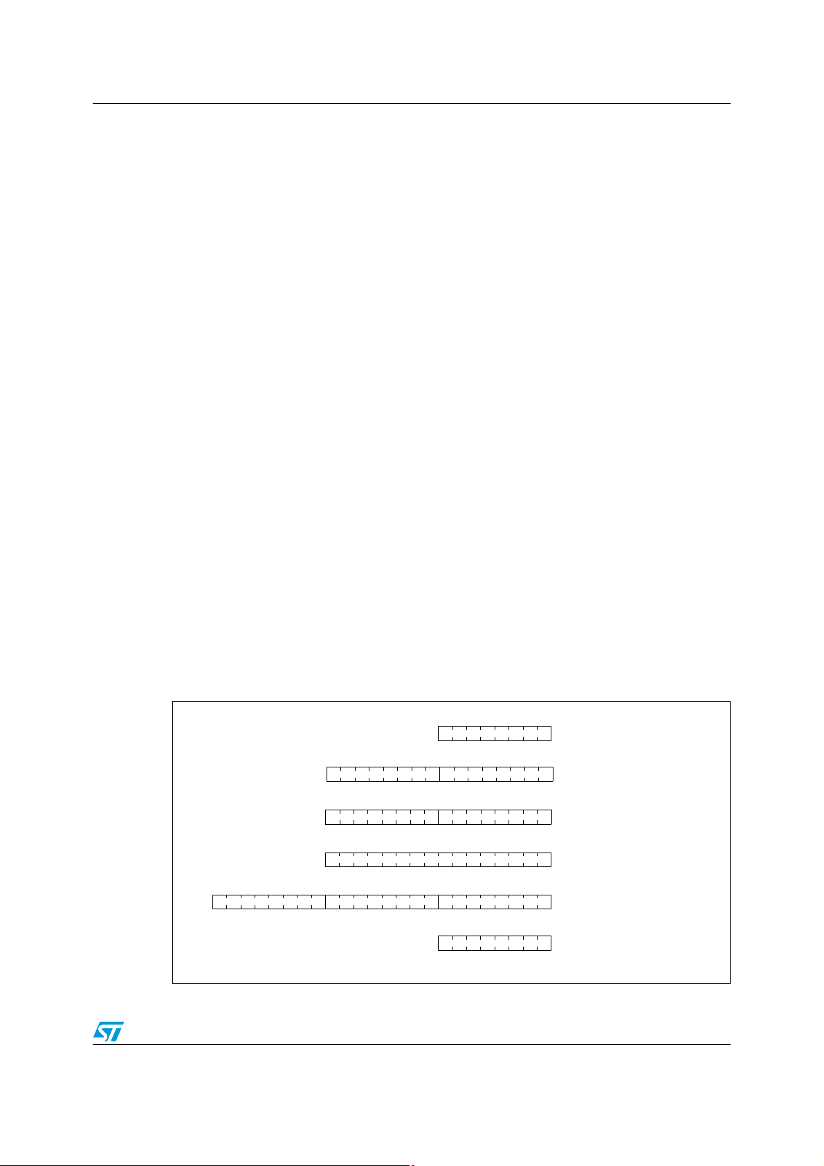
Figure 1. Programming model . . . . . . . . . . . . . . . . . . . . . . . . . . . . . . . . . . . . . . . . . . . . . . . . . . . . . . 13
Figure 2. Context save/restore for interrupts . . . . . . . . . . . . . . . . . . . . . . . . . . . . . . . . . . . . . . . . . . . 14
Figure 3. Address spaces . . . . . . . . . . . . . . . . . . . . . . . . . . . . . . . . . . . . . . . . . . . . . . . . . . . . . . . . . 18
Figure 4. Memory Interface Architecture . . . . . . . . . . . . . . . . . . . . . . . . . . . . . . . . . . . . . . . . . . . . . . 19
Figure 5. Pipelined execution principle . . . . . . . . . . . . . . . . . . . . . . . . . . . . . . . . . . . . . . . . . . . . . . . 20
Figure 6. Pipelined execution stages . . . . . . . . . . . . . . . . . . . . . . . . . . . . . . . . . . . . . . . . . . . . . . . . . 21
Figure 7. Immediate addressing mode example . . . . . . . . . . . . . . . . . . . . . . . . . . . . . . . . . . . . . . . . 34
Figure 8. Short Direct addressing mode example . . . . . . . . . . . . . . . . . . . . . . . . . . . . . . . . . . . . . . . 36
Figure 9. Long Direct addressing mode example . . . . . . . . . . . . . . . . . . . . . . . . . . . . . . . . . . . . . . . 37
Figure 10. Far Direct addressing mode example . . . . . . . . . . . . . . . . . . . . . . . . . . . . . . . . . . . . . . . . 38
Figure 11. No Offset Indexed addressing mode example . . . . . . . . . . . . . . . . . . . . . . . . . . . . . . . . . . 40
Figure 12. Short Indexed - 8-bit offset - addressing mode example . . . . . . . . . . . . . . . . . . . . . . . . . . 41
Figure 13. SP Indexed - 8-bit offset - addressing mode example . . . . . . . . . . . . . . . . . . . . . . . . . . . . 42
Figure 14. Long Indexed - 16-bit offset - addressing mode example. . . . . . . . . . . . . . . . . . . . . . . . . . 43
Figure 15. Far Indexed - 16-bit offset - addressing mode example . . . . . . . . . . . . . . . . . . . . . . . . . . . 44
Figure 16. Short Pointer Indirect Long addressing mode example . . . . . . . . . . . . . . . . . . . . . . . . . . . 46
Figure 17. Long Pointer Indirect Long addressing mode example . . . . . . . . . . . . . . . . . . . . . . . . . . . 47
Figure 18. Short Pointer Indirect Long Indexed addressing mode example . . . . . . . . . . . . . . . . . . . . 50
Figure 19. Long Pointer Indirect Long Indexed addressing mode example. . . . . . . . . . . . . . . . . . . . . 52
Figure 20. Long Pointer Indirect Extended Indexed addressing mode example . . . . . . . . . . . . . . . . . 54
Figure 21. Relative Direct addressing mode example . . . . . . . . . . . . . . . . . . . . . . . . . . . . . . . . . . . . . 56
Figure 22. Bit Long Direct addressing mode example . . . . . . . . . . . . . . . . . . . . . . . . . . . . . . . . . . . . . 58
Figure 23. Bit Long Direct Relative addressing mode example . . . . . . . . . . . . . . . . . . . . . . . . . . . . . . 60
8/162 Doc ID 13590 Rev 3
Page 9

PM0044 STM8 architecture
1 STM8 architecture
The 8-bit STM8 Core is designed for high code efficiency. It contains 6 internal registers, 20
addressing modes and 80 instructions. The 6 internal registers include two 16-bit Index
registers, an 8-bit Accumulator, a 24-bit Program Counter, a 16-bit Stack Pointer and an 8-
bit Condition Code register. The two Index registers X and Y enable Indexed Addressing
modes with or without offset, along with read-modify-write type data manipulation. These
registers simplify branching routines and data/arrays modifications.
The 24-bit Program Counter is able to address up to 16-Mbyte of RAM, ROM or Flash
memory. The 16-bit Stack Pointer provides access to a 64K-level Stack. The Core also
includes a Condition Code register providing 7 Condition flags that indicate the result of the
last instruction executed.
The 20 Addressing modes, including Indirect Relative and Indexed addressing, allow
sophisticated branching routines or CASE-type functions. The Indexed Indirect Addressing
mode, for instance, permits look-up tables to be located anywhere in the address space,
thus enabling very flexible programming and compact C-based code. The stack pointer
relative addressing mode permits optimized C compiler stack model for local variables and
parameter passing.
The Instruction Set is 8-bit oriented with a 2-byte average instruction size. This Instruction
Set offers, in addition to standard data movement and logic/arithmetic functions, 8-bit by 8-
bit multiplication, 16-bit by 8-bit and 16-bit by 16-bit division, bit manipulation, data transfer
between Stack and Accumulator (Push / Pop) with direct stack access, as well as data
transfer using the X and Y registers or direct memory-to-memory transfers.
The number of Interrupt vectors can vary up to 32, and the interrupt priority level may be
managed by software providing hardware controlled nested capability. Some peripherals
include Direct Memory Access (DMA) between serial interfaces and memory. Support for
slow memories allows easy external code execution through serial or parallel interface
(ROMLESS products for instance).
The STM8 has a high energy-efficient architecture, based on a Harvard architecture and
pipelined execution. A 32-bit wide program memory bus allows most of the instructions to be
fetched in 1 CPU cycle. Moreover, as the average instruction length is 2 bytes, this allows for
a reduction in the power consumption by only accessing the program memory half of the
time, on average. The pipelined execution allowed the execution time to be minimized,
ensuring high system performance, when needed, together with the possibility to reduce the
overall energy consumption, by using different power saving operating modes. Power-saving
can be managed under program control by placing the device in SLOW, WAIT, SLOW-WAIT,
ACTIVE-HALT or HALT mode (see product datasheet for more details).
Doc ID 13590 Rev 3 9/162
Page 10

STM8 architecture PM0044
Additional blocks
The additional blocks take the form of integrated hardware peripherals arranged around the
central processor core. The following (non-exhaustive) list details the features of some of the
currently available blocks:
Boot ROM Memory area containing the bootloader code
Flash Flash-based devices
RAM Sizes up to several Kbytes
Data EEPROM
Timers
A/D converter
I2C
SPI
USART
Watchdog
I/O ports
Sizes up to several Kbytes. Erase/programming operations do not require
additional external power sources.
Different versions based on 8/16-bit free running or autoreload timer/counter are
available. They can be coupled with either input captures, output compares or
PWM facilities. PWM functions can have software programmable duty cycle
between 0% to 100% in up to 256/65536 steps. The outputs can be filtered to
provide D/A conversion.
The Analog to Digital Converter uses a sample and hold technique. It has 12-bit
resolution.
Multi/master, single master, single slave modes, DMA or 1byte transfer, standard
and fast I2C modes, 7 and 10-bit addressing.
The Serial peripheral Interface is a fully synchronous 3/4 wire interface ideal for
Master and Slave applications such as driving devices with input shift register
(LCD driver, external memory,...).
The USART is a fast synchronous/asynchronous interface which features both
duplex transmission, NRZ format, programmable baud rates and standard error
detection. The USART can also emulate RS232 protocol.
It has the ability to induce a full reset of the MCU if its counter counts down to
zero prior to being reset by the software. This feature is especially useful in noisy
applications.
They are programmable by software to act in several input or output
configurations on an individual line basis, including high current and interrupt
generation. The basic block has eight bit lines.
1.1 STM8 development support
The STM8 family of MCUs is supported by a comprehensive range of development tools.
This family presently comprises hardware tools (emulators, programmers), a software
package (assembler-linker, debugger, archiver) and a C-compiler development tool.
STM8 and ST7 CPUs are supported by a single toolchain allowing easy reuse and
portability of the applications between product lines.
10/162 Doc ID 13590 Rev 3
Page 11

PM0044 STM8 architecture
1.2 Enhanced STM8 features
● 16-Mbyte linear program memory space with 3 FAR instructions (CALLF, RETF, JPF)
● 16-Mbyte linear data memory space with 1 FAR instruction (LDF)
● Up to 32 24-bit interrupt vectors with optimized context save management
● 16-bit Stack Pointer (SP=SH:S) with stack manipulation instructions and addressing
modes
● New register and memory access instructions (EXG, MOV)
● New arithmetic instructions: DIV 16/8 and DIVW 16/16
● New bit handling instructions (CCF, BCPL, BCCM)
● 2 x 16-bit index registers (X=XH:XL, Y=YH:YL). 8-bit data transfers address the low
byte. The high-byte is not affected, with a reset value of 0. This allows the use of X/Y as
8-bit values.
● Fast interrupt handling through alternate register files (up to 4 contexts) with standard
stack compatible mode (for real time OS kernels)
● 16-bit/8-bit stack operations (X, Y, A, CC stacking)
● 16-bit pointer direct update with 16-bit relative offset (ADDW/SUBW for X/Y/SP)
● 8-bit & 16-bit arithmetic and signed arithmetic support
Doc ID 13590 Rev 3 11/162
Page 12

Glossary PM0044
2 Glossary
mnem mnemonic
src source
dst destination
cy duration of the instruction in CPU clock cycles (internal clock)
lgth length of the instruction in byte(s)
op-code instruction byte(s) implementation (1..4 bytes), operation code.
mem memory location
imm immediate value
off offset
ptr pointer
pos position
byte a byte
word 16-bit value
short represent a short 8-bit addressing mode
long represent a long 16-bit addressing mode
EA Effective Address: The final computed data byte address
Page Zero all data located at [00..FF] addressing space (single byte address)
(XX) content of a memory location XX
XX a byte value
ExtB Extended byte
MS Most Significant byte of a 16-bit value (MSB)
LS Least Significant byte of a 16-bit value (LSB)
A Accumulator register
X 16-bit X Index register
Y 16-bit Y Index register
reg A, XL or YL register (1-byte LS part of X/Y), XH or YH (1-byte MS part of X/Y)
ndx index register, either X or Y
PC 24-bit Program Counter register
SP 16-bit Stack Pointer
S Stack Pointer LSB
CC Condition Code register
12/162 Doc ID 13590 Rev 3
Page 13
PM0044 STM8 core description
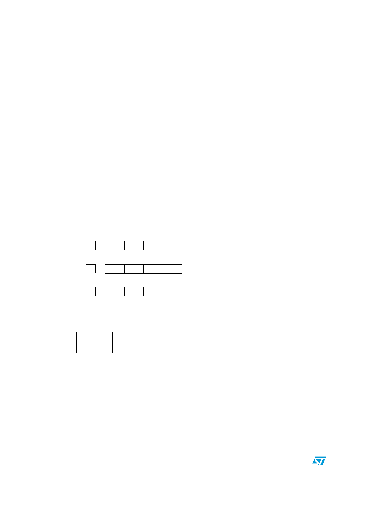
07
A ACCUMULATOR
015
SP STACK POINTER
X INDEX
Y INDEX
07815
PC PROGRAM COUNTER
PCH PCL
07
CC CODE CONDITION
V
-
I1 H I0 N Z C
1623
PCE
07815
XH XL
07815
YH YL
3 STM8 core description
3.1 Introduction
The CPU has a full 8-bit architecture, with 16-bit operations on index registers (for address
computation). Six internal registers allow efficient 8-bit data manipulation. The CPU is able
to execute 80 basic instructions. It features 20 addressing modes and can address 6 internal
registers and 16 Mbytes of memory/peripheral registers.
3.2 CPU registers
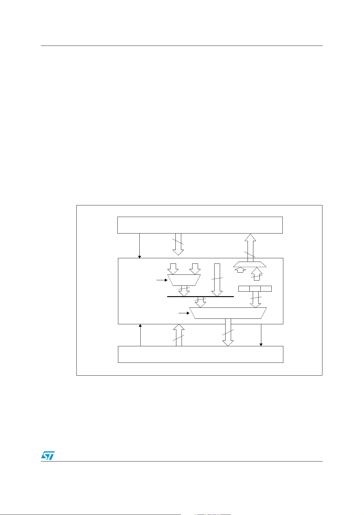
The 6 CPU registers are shown in the programming model in Figure 1. Following an
interrupt, the register context is saved. The context is saved by pushing registers onto the
stack in the order shown in Figure 2. They are popped from the stack in the reverse order.
Accumulator (A)
The accumulator is an 8-bit general purpose register used to hold operands and the results
of the arithmetic and logic calculations as well as data manipulations.
Index registers (X and Y)
These 16-bit registers are used to create effective addresses or as temporary storage area
for data manipulations. In most of the cases, the cross assembler generates a PRECODE
instruction (PRE) to indicate that the following instruction refers to the Y register. Both X and
Y are automatically saved on interrupt routine branch.
Program Counter (PC)
The program counter is a 24-bit register used to store the address of the next instruction to
be executed by the CPU. It is automatically refreshed after each processed instruction. As a
result, the STM8 core can access up to 16-Mbytes of memory.
Figure 1. Programming model
Doc ID 13590 Rev 3 13/162
Page 14

STM8 core description PM0044
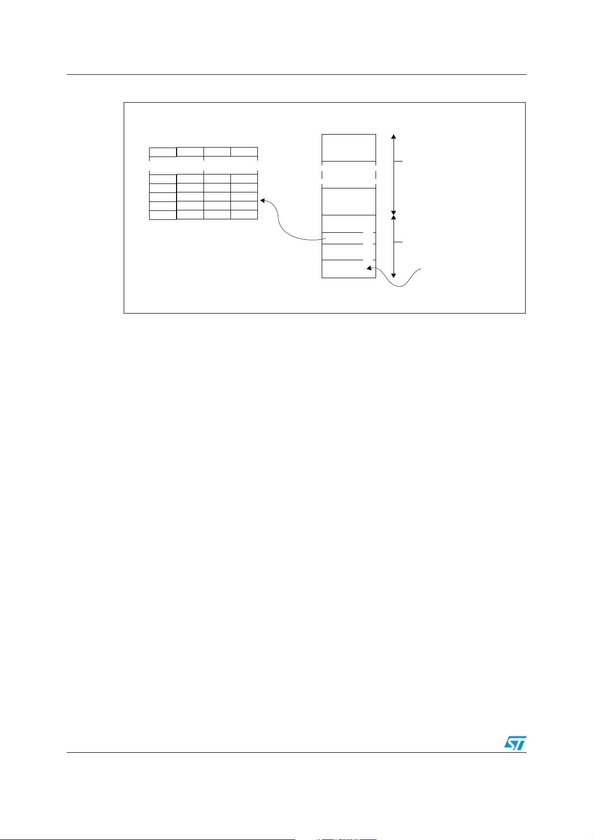
Stack Pointer (SP)
The stack pointer is a 16-bit register. It contains the address of the next free location of the
stack. Depending on the product, the most significant bits can be forced to a preset value.
The stack is used to save the CPU context on subroutines calls or interrupts. The user can
also directly use it through the POP and PUSH instructions.
After an MCU reset the Stack Pointer is set to its upper limit value. It is then decremented
after data has been pushed onto the stack and incremented after data is popped from the
stack. When the lower limit is exceeded, the stack pointer wraps around to the stack upper
limit. The previously stored information is then overwritten, and therefore lost.
A subroutine call occupies two or three locations.
When an interrupt occurs, the CPU registers (CC, X, Y, A, PC) are pushed onto the stack.
This operation takes 9 CPU cycles and uses 9 bytes in RAM.
Note: The WFI/HALT instructions save the context in advance. If an interrupt occurs while the CPU
is in one of these modes, the latency is reduced.
Figure 2. Context save/restore for interrupts
).4%22504'%.%2!4)/.EXECUTEPIPELINE
#OMPLETEINSTRUCTIONINEXECUTESTAGECYCLELATENCY
053(0#,
053(0#(
053(0#%
053(9
053(8
053(!
053(##
*5-04/).4%225042/54).%')6%."94(%).4%225046%#4/2
).4%225042/54).%
%8%#54)/.
)2%4).3425#4)/.
0/0##
0/0!
0/08
0/09
0/00#%
0/00#(
0/00#,
#05#9#,%3
5.34!#+
0/0
#05#9#,%3
2%4 5
2.
0#,
0#,
0#(
0#,
0#%
0#,
9,
0#,
9(
0#,
8,
0#,
8(
0#,
!
0#,
##
0#,
).4%22504
34!#+
053(
*5-04/4(%!$$2%33')6%."902/'2!-#/5.4%22ELOAD0IPELINE
14/162 Doc ID 13590 Rev 3
-36
Page 15
PM0044 STM8 core description
Global configuration register (CFG_GCR)
The global configuration register is a memory mapped register. It controls the configuration
of the processor. It contains the AL control bit:
AL: Activation level
If the AL bit is 0 (main), the IRET will cause the context to be retrieved from stack and the
main program will continue after the WFI instruction.
If the AL bit is 1 (interrupt only active), the IRET will cause the CPU to go back to WFI/HALT
mode without restoring the context.
This bit is used to control the low power modes of the MCU. In a very low power application,
the MCU spends most of the time in WFI/HALT mode and is woken up (through interrupts)
at specific moments in order to execute a specific task. Some of these recurring tasks are
short enough to be treated directly in an ISR, rather than going back to the main program. In
this case, by programming the AL bit to 1 before going to low power (by executing WFI/HALT
instruction), the run time/ISR execution is reduced due to the fact that the register context is
not saved/restored each time.
Condition Code register (CC)
The Condition Code register is a 8-bit register which indicates the result of the instruction
just executed as well as the state of the processor. These bits can be individually tested by a
program and specified action taken as a result of their state. The following paragraphs
describe each bit.
● V: Overflow
When set, V indicates that an overflow occurred during the last signed arithmetic
operation, on the MSB operation result bit. See INC, INCW, DEC, DECW, NEG, NEGW,
ADD, ADC, SUB, SUBW, SBC, CP, CPW instructions.
● I1: Interrupt mask level 1
The I1 flag works in conjunction with the I0 flag to define the current interruptability level
as shown in the following table. These flags can be set and cleared by software through
the RIM, SIM, HALT, WFI, IRET, TRAP and POP instructions and are automatically set
by hardware when entering an interrupt service routine.
Table 1. Interruptability levels
Interruptability Priority I1 I0
Interruptable Main
Interruptable Level 1 01
Interruptable Level 2 00
Non Interruptable 11
● H: Half carry bit
Lowest
↕
Highest
10
The H bit is set to 1 when a carry occurs between the bits 3 and 4 of the ALU during an
ADD or ADC instruction. The H bit is useful in BCD arithmetic subroutines.
For ADDW, SUBW it is set when a carry occurs from bit 7 to 8, allowing to implement
byte arithmetic on 16-bit index registers.
Doc ID 13590 Rev 3 15/162
Page 16
STM8 core description PM0044
● I0: Interrupt mask level 0
See Flag I1
● N: Negative
When set to 1, this bit indicates that the result of the last arithmetic, logical or data
manipulation is negative (i.e. the most significant bit is a logic 1).
● Z: Zero
When set to 1, this bit indicates that the result of the last arithmetic, logical or data
manipulation is zero.
● C: Carry
When set, C indicates that a carry or borrow out of the ALU occurred during the last
arithmetic operation on the MSB operation result bit (bit 7 for 8-bit result/destination or
bit 15 for 16-bit result). This bit is also affected during bit test, branch, shift, rotate and
load instructions. See ADD, ADC, SUB, SBC instructions.
In bit test operations, C is the copy of the tested bit. See BTJF, BTJT instructions.
In shift and rotates operations, the carry is updated. See RRC, RLC, SRL, SLL, SRA
instructions.
This bit can be set, reset or complemented by software using SCF, RCF, CCF
instructions.
Example: Addition
$B5 + $94 = "C" + $49 = $149
C7 0
0 10110101
C7 0
+0 10010100
C7 0
=1 01001001
The results of each instruction on the Condition Code register are shown by tables in
Section 7: STM8 instruction set. The following table is an example:
VI1HI0NZC
V0 0NZ1
where
Nothing = Flag not affected
Flag name =Flag affected
0 = Flag cleared
1 = Flag set
16/162 Doc ID 13590 Rev 3
Page 17

PM0044 STM8 memory interface
4 STM8 memory interface
4.1 Program space
The program space is 16-Mbyte and linear. To distinguish the 1, 2 and 3 byte wide
addressing modes, naming has been defined as shown in Figure 3:
● "Page" [0xXXXX00 to 0xXXXXFF]: 256-byte wide memory space with the same two
most significant address bytes (XXXX defines the page number).
● "Section" [0xXX0000 to 0xXXFFFF]: 64-Kbyte wide memory space with the same most
significant address byte (XX defines the section number).
The reset and interrupt vector table are placed at address 0x8000 for the STM8 family.
(Note: the base address may be different for later implementations.) The table has 32 4-byte
entries: RESET, Trap, NMI and up to 29 normal user interrupts. Each entry consists of the
reserved op-code 0x82, followed by a 24-bit value: PCE, PCH, PCL address of the
respective Interrupt Service Routine. The main program and ISRs can be mapped
anywhere in the 16 Mbyte memory space.
CALL/CALLR and RET must be used only in the same section. The effective address for the
CALL/RET is used as an offset to the current PCE register value. For the JP, the effective
address 16 or 17-bit (for indexed addressing) long, is added to the current PCE value. In
order to reach any address in the program space, the JPF jump and CALLF call instructions
are provided with a three byte extended addressing mode while the RETF pops also three
bytes from the stack.
As the memory space is linear, sections can be crossed by two CPU actions: next
instruction byte fetch (PC+1), relative jumps and, in some cases, by JP (for indexed
addressing mode).
Note: For safe memory usage, a function which crosses sections MUST:
- be called by a CALLF
- include only far instructions for code operation (CALLF & JPF)
All label pointers are located in section 0 (JP [ptr.w] example: ptr.w is located in section 0
and the jump address in current section)
Any illegal op-code read from the program space triggers a MCU reset.
4.2 Data space
The data space is 16-Mbyte and linear. As the stack must be located in section 0 and as
data access outside section 0/1 can be managed only with LDF instructions, frequently used
data should be located in section 0 to get the optimum code efficiency.
All data pointers are located in section 0 only.
Indexed addressing (with 16-bit index registers and long offset) allows data access over
section 0 and 1.
All the peripherals are memory mapped in the data space.
Doc ID 13590 Rev 3 17/162
Page 18
STM8 memory interface PM0044
VECTORS
PAGE 0
0x000000
0x0000FF
0x00807F
0x00FFFF
0x010000
0x01FFFF
0xFF0000
0xFFFFFF
1-BYTE ADDRESSING MODE
BIT HANDLING CAPABILITY
2-BYTE ADDRESSING MODE
3-BYTE ADDRESSING MODE
FAST DATA ACCESS WITH
DATA SPACE
SECTION 0
SECTION 1
SECTION 256
RESET
L
RESET
H
TRAP
L
TRAP
H
NMI
L
NMI
H
INT0
L
INT0
H
INT1
L
INT1
H
INT28
L
INT28
H
0x00807C
0x008000
PROGRAM SPACE
BIT HANDLING CAPABILITY
POWERFUL DATA MANAGEMENT
ACCESSIBLE DATA
STACK AREA
SHORT GENERATED CODE
RESET
E
TRAP
E
NMI
E
INT0
E
INT1
E
INT28
E
0x008000
POINTERS
0x82
0x82
0x82
0x82
0x82
0x82
Figure 3. Address spaces
18/162 Doc ID 13590 Rev 3
Page 19
PM0044 STM8 memory interface
PCE PCH PCL
PROGRAM COUNTER
Data@E Data@E0:H:L0x00
YN
"LDF" INSTRUCTION
@DATABUS
RAM FETCH INSTRUCTION
YN
CPU
Memory Interface (RAM)
STALL
A15..0
7
24
17
24
D7..0
R/W
DATABUS
@BUS
Memory Interface (Flash)
STALL
A23..0
D31..0
DATABUS
@BUS
(FETCH)
24
@DATABUS
24
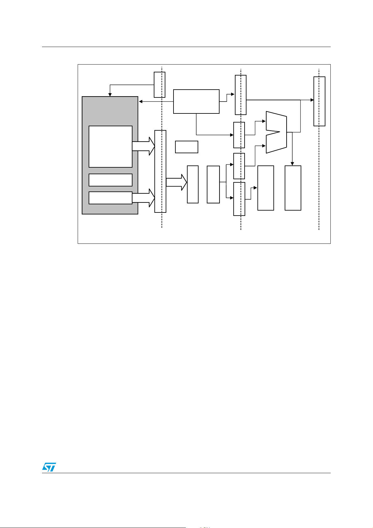
4.3 Memory interface architecture
The STM8 uses a Harvard architecture, with separate program and data memory buses.
However, the logical address space is unified, all memories sharing the same 16-Mbytes
space, non-overlapped. The memory interfaces are shown in Figure 4. It consists of two
buses: address, data, read/write control signal (R/W) and memory acknowledge signal
(STALL).
The STALL acknowledge signal makes the CPU compatible with slow serial or parallel
memory interfaces. When the memory interface is slow the CPU waits the memory
acknowledge before executing the instruction. So in such a case, the instruction CPU cycle
time is prolonged compare to the value given in this manual.
The program memory bus is 32-bit wide, allowing the fetch of most of the instructions in one
cycle.
As the address space is unified, the architecture allows data to be stored also in the Flash
memory and program to be fetched also from RAM (data bus). In this later case the
performance is impacted, besides the fact that data and fetch operation share the same bus,
the instructions will be fetched one byte at a time, thus taking longer (1 cycle /byte).
Figure 4. Memory Interface Architecture
Doc ID 13590 Rev 3 19/162
Page 20
Pipelined execution PM0044
-36
%8%#54%
$%#/$%
&%4#(
0#N
0#
0#N
)NSTRUCTIONSSFETCHEDFROMMEMORY
)NSTRUCTIONSDECODINGANDDATAREADFROMMEMORYIFNEEDED
2EGISTERSDATAREADFROMREGISTERBANK
3HIFTAND!,5OPERATION
7RITEBACKREGISTERSDATATO2EGISTERBANK
7RITEBACKDATATOMEMORY
5 Pipelined execution
The STM8 family uses a 3-stage pipeline to increase the speed of the flow of instructions
sent to the processor. Pipelined execution allows several operations to be performed
simultaneously, rather than serially:
● Fetch
● Decode and address
● Execute
The Program Counter (PC) points always to the instruction in decode stage as shown in
Figure 5.
Figure 5. Pipelined execution principle
5.1 Description of pipelined execution stages
Figure 6 and Section 5.1.1, Section 5.1.2, and Section 5.1.3 provide a detailed description
of each stage of the pipeline execution.
20/162 Doc ID 13590 Rev 3
Page 21
PM0044 Pipelined execution
-36
&ETCH $ECODE-EM2EAD %XECUTE7RITEBACK
!,5
%XECUTION
2EGISTER
!LIGN
-%-/29
#/.42/,
2!-
0ERIPHERALS
&LASH
INSTRUCTION
MEMORY
BIT
BIT
0REFETCHBUFFER
BIT
!DDRESS
COMPUTATION
/PCODE
)MM
7"ADD
-RD
$ECODE
0#
)4#
7RITE"ACK
Figure 6. Pipelined execution stages
5.1.1 Fetch stage
The first pipeline stage includes a 64-bit fetch buffer and a 32-bit prefetch buffer, totalling 3
words named F
to be available for decoding immediately after F
The instruction access from Flash Program memory is 32-bit wide and it is performed from
an aligned address i.e. 0xXXX0, 0xXXX4, 0xXXX8, or 0xXXXC.
Unlike the decode and execute stages that are performed at every cycle, the fetch stage
accesses the program memory only when needed, and stops memory access when the
buffer is full. This allows reducing the core power consumption,
Reading program from RAM is similar to reading program from ROM. However, since the
RAM data bus is 8-bit wide, 4 consecutive read operations have to be performed to load one
word, thus resulting in RAM execution being slower than Flash execution.
F
X
5.1.2 Decoding and addressing stage
The decoding stage includes an instruction alignment unit. The alignment unit uses the 64bit input from the fetch unit and feeds an instruction (from 1 to 5 bytes depending on the
instruction) to the decoding unit.
The instruction code consists of 2 parts (see examples in Table 2 ):
● The op-code itself (1 or 2 bytes)
● and a data/address part (0 to 3 bytes).
, F2 and F3. This buffer structure allows any instruction code (up to 5 bytes)
1
(and F2 when needed) is/are loaded.
1
Doc ID 13590 Rev 3 21/162
Page 22
Pipelined execution PM0044
The op-code is decoded in this stage. When present, the instruction address is used for
address computation, whilst the immediate operand is forwarded to the execution stage.
Table 2. Data/address decoding examples
Instruction Syntax Op-code Data/address
Register to register
move
Register load LD A,($12,SP) 0x7B 0x12
Register store LD ($12,SP),A 0x6B 0x12
Data load / store with
extended address
Long/unaligned instructions
For long instructions (i.e. 5-bytes instructions), the fetch may need 2 program memory
accesses to be completed. In this case, the decoding stage (after decoding the op-code
part), is stalled waiting for the fetch stage to complete the 2nd fetch.
In case of shorter instructions, this may also happen when they cross a 32-bit boundary.
Indirect addressing
For indirect addressing, the CPU is stalled in this stage to read the pointer from the data
memory (i.e. RAM). The number of cycles during which the CPU is stalled depends on the
pointer size (short, long or extended addressing mode).
5.1.3 Execution stage
In the execution stage, the operation is executed and the result is stored in the accumulator,
index register or RAM.
LD A, XH 0x95 -
LDF A,($123456,Y) 0x90 AF 0x12 34 56
5.2 Data memory conflicts
3 types of operations perform accesses to the data memory:
● Effective address computation in case of indirect addressing
● Data read: source operand
● Data write: destination for store or read-modify-write operations
In case of simultaneous accesses to the same memory area both in execution stage (write)
and decoding stage (read), the decode stage is stalled till the execution stage releases the
resource.
22/162 Doc ID 13590 Rev 3
Page 23
PM0044 Pipelined execution
C
y
DecCy ExeCy 1–+=
5.3 Pipelined execution examples
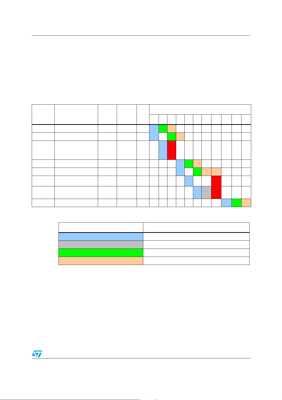
A few pipelined execution examples are reported below. The numbers of cycles for the
decoding and execution stages correspond to the minimum number of cycles needed by the
instruction itself. In some cases, depending on the instruction sequence, the cycle taken
could be more than that number.
5.4 Conventions
Although the decode and/or execute stage of some instructions may take a different number
of cycles, a simplified convention providing a good match with reality, has been used in this
section:
● The decode stage of each instruction takes one cycle only
● The execution stage takes a number of cycles equal to
Where
C
is the number of execution cycles. In case of decode and execute cycles, It
y
corresponds to the minimum number of cycles needed by the instruction itself, and
does not take into account the impact of the instruction sequence.
DecCy is the exact number of decode cycles.
ExeCy is the exact number of execute cycles.
The decode stage of the next instruction starts during the last execution cycle. In
instructions performing pipeline flush, the convention is that, in case the branch is taken, the
next fetch are performed during the last instruction execution cycle.
The exact number of cycles (see Tab l e 3 ) and the number of cycles obtained using this
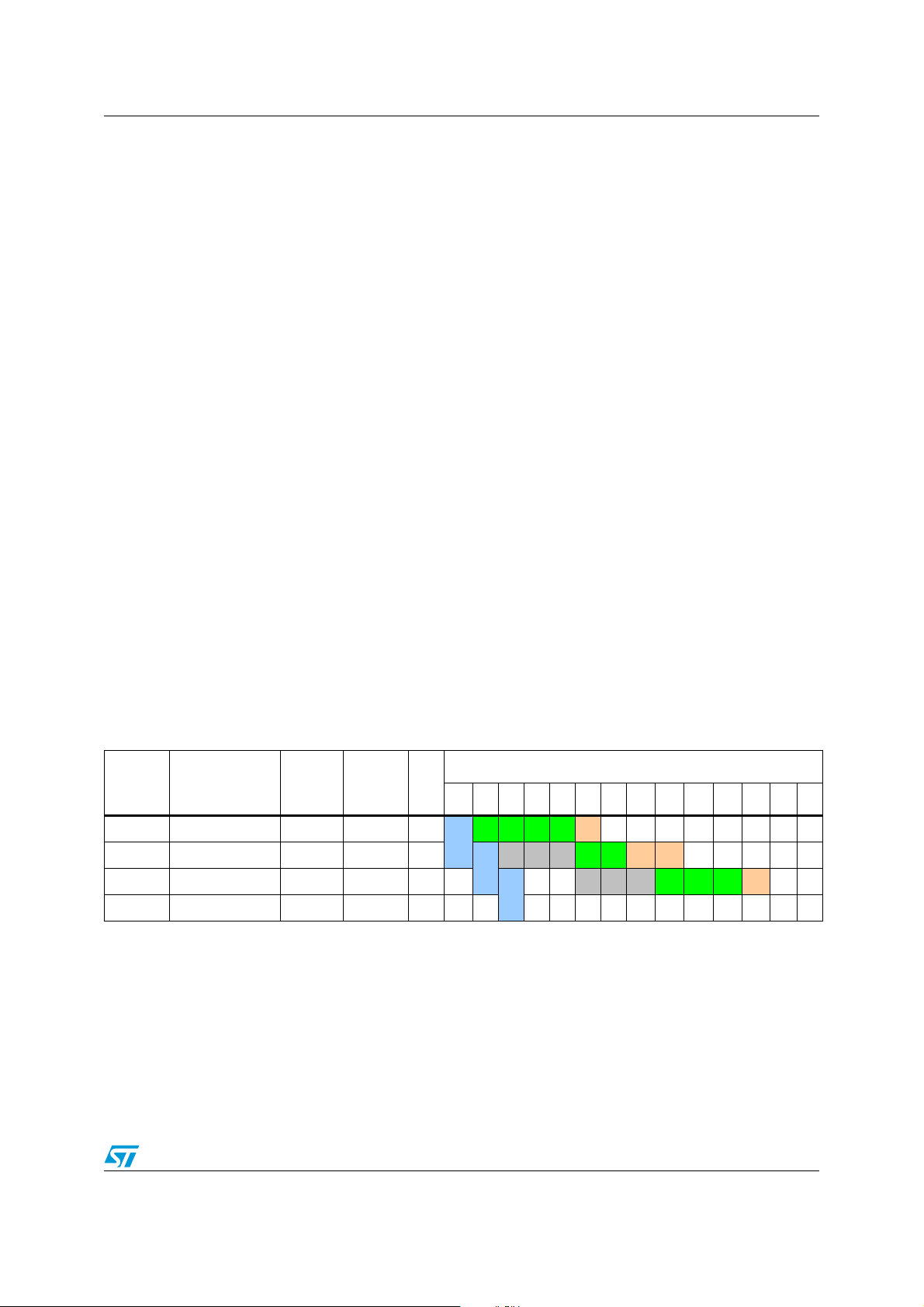
convention (see Tab l e 4 ) are identical.
Table 3. Example with exact number of cycles
Address Instruction
0xC000 LDW X, [$50.w] 4 1 3
0xC003 ADDW X, #20 2 2 3
0xC006 LD A, [$30].w 3 1 3
0xC009 ….
Decode
cycles
Execute
cycles
lgth
F
Time (cycle)
1 2 3 4 5 6 7 8 9 10 11 12 13 14
D D D D E
1
D D D D D E E
F
2
F
3
D D D D D D E
Doc ID 13590 Rev 3 23/162
Page 24
Pipelined execution PM0044
Table 4. Example with conventional number of cycles
Address Instruction
0xC000 LDW X, [$50.w] 4 3 3
0xC003 ADDW X, #20 3 3 3
0xC006 LD A, [$30].w 3 3 3
Decode
cycles
Execute
cycles
lgth
1 234567 8 91011121314
Time (cycle)
D E E E E
F
1
D D D D E E E
F
2
F
3
D D D D
E E E
0xC009 ….
Table 5. Legend
Symbol/Color Definition
FFetch
D Decode stalled
DDecode
EExecute
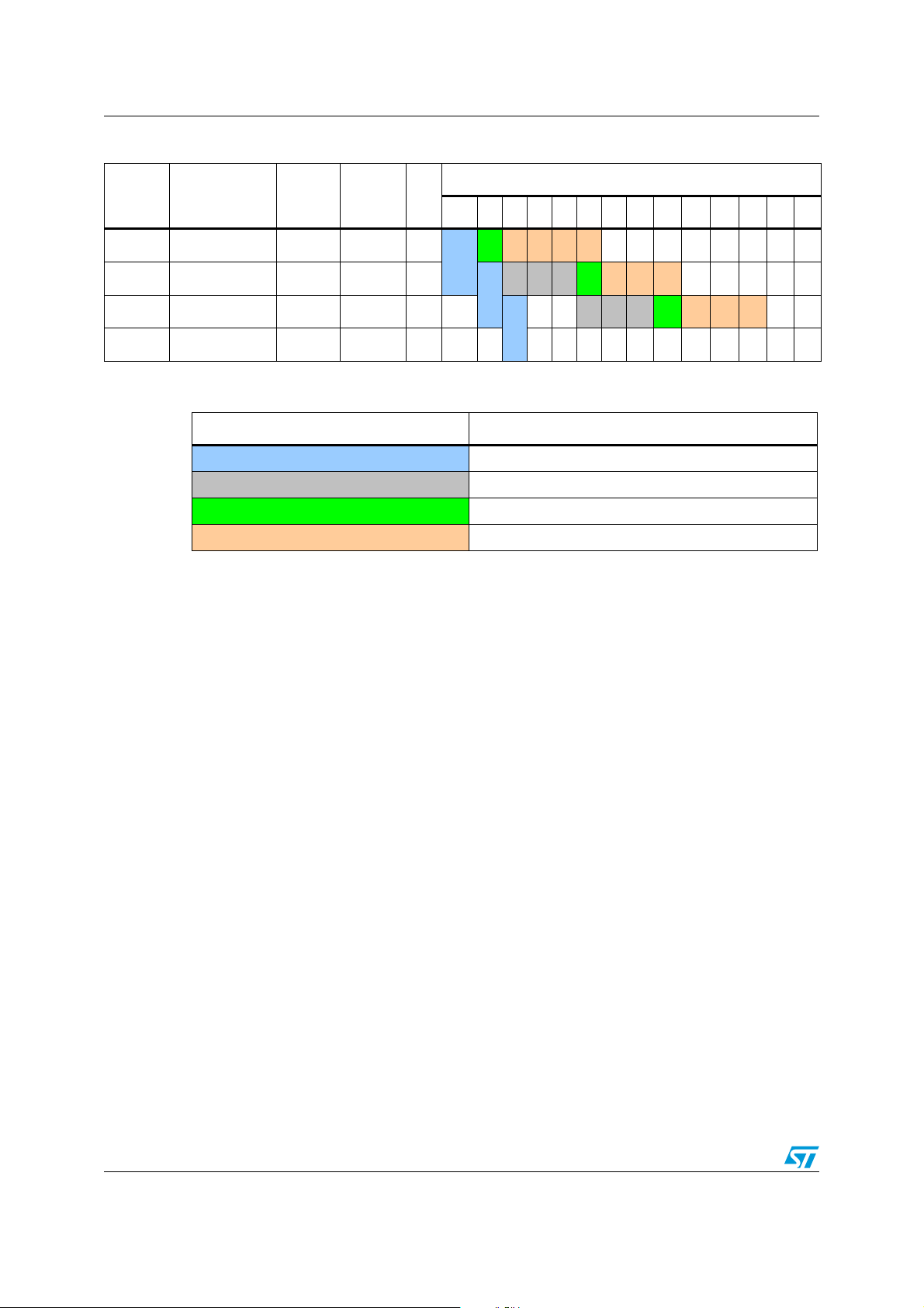
5.4.1 Optimized pipeline example – execution from Flash Program memory
In the example shown in Tab l e 6 , the code is stored in the Flash Program memory (32-bit
bus). As a result, 3 cycles are needed to fill the 96-bit prefetch buffer. At each cycle, one
word is loaded and stored in F
the instructions contained in one of the F
instruction contained in F
, F2 and F3. The next fetch operation can start only when all
1
(SWAP A) is decoded, and a fetch operation can start to fill F
3
word are decoded. In fact, at cycle 9, the last
x
word.
3
24/162 Doc ID 13590 Rev 3
Page 25
PM0044 Pipelined execution
Table 6. Optimized pipeline example - execution from Flash
Add. Instruction
0xC000 NEG A 1 1 1
0xC001 XOR A, $10 1 1 2
0xC003 LD A, #20 1 1 2
0xC005 SUB A,$1000 1 1 3
Decod.
cycles
Exec.
cycles
lgth
1234567891011121314
D E
F
1
D E
D E
F
2
0xC008 INC A 1 1 1
0xC009 LD XL, A 1 1 1
F
0xC00A SRL A 1 1 1
3
0xC00B SWAP A 1 1 1
0xC00C SLA $15 1 1 2
F
0xC00E CP A,#$FE 1 1 2
1
0xC010 MOV $100, #11 1 1 4
0xC014 MOV $101, #22 1 1 4
Table 7. Legend
D E
F
2
D E
Cycle
D E
D E
D E
F
3
D E
D E
D E
D E
Symbol/Color Definition
FFetch
DDecode
EExecute
Doc ID 13590 Rev 3 25/162
Page 26
Pipelined execution PM0044
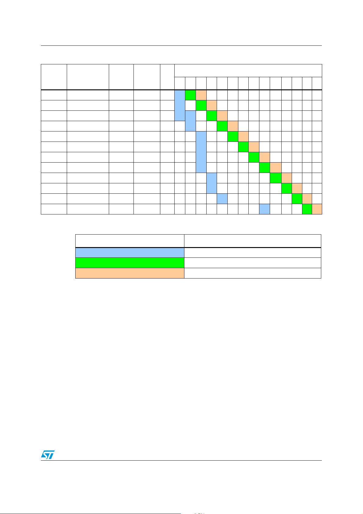
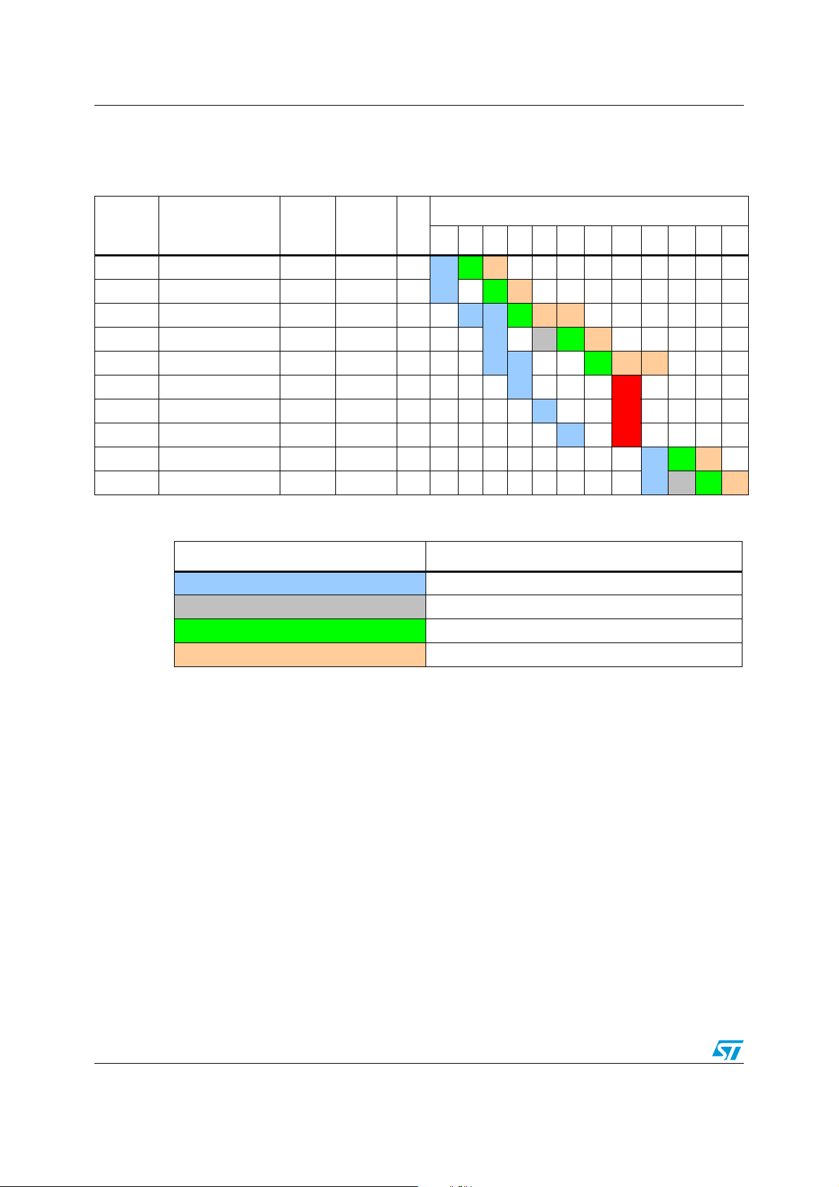
5.4.2 Optimize pipeline example – execution from RAM
In the example shown in Tab l e 8 , the RAM is accessed through an 8-bit bus. As a result, 12
cycles are required to fill the 96-bit pre-fetch buffer. Every 4 cycles, one word is loaded and
stored in F
filled. This occurs for example till the 4
decoded only at the 5
In case of read/write access to the RAM, the fetch is stalled. This occurs during the 6
since RAM address 10 is read during the decode stage of XOR A, $10.
Table 8. Optimize pipeline example – execution from RAM
. The decoding of the first word instruction can start only when the Fx word is
x
th
cycle.
th
cycle, and the first instruction (NEG A) can be
Cycle
th
cycle
Add.
Instruction
0xC000 NEG A 1 1 1
0xC001
0xC003 LD A, #20 1 1 2
0xC005
0xC008 INC A 1 1 1
0xC009 LD XL, A 1 1 1
0xC00A SRL A 1 1 1
0xC00B SWAP A 1 1 1
0xC00C SLA $15 1 1 2
0xC00E
XOR A,
$10
SUB
A,$1000
CP
A,#$FE
Table 9. Legend
Decode cycles
Execute cycles
112
113
112
lgth
1 2 3 4 5 6 7 8 9 10 11 12 13 14 15 16 17 18 19 20 21
D D D D E
1_1
F
1_4F2_1
F
D E
D D D D E
FS
2_2F2_3F2_4
F
D E
D D D D E
3_1
F
FS
3_2
F
F
3_3
F
3_4
D E
1_1F1_2
F
D E
1_3F1_4
F
D E
D E
D E
1_2F1_3
F
Symbol/Color Definition
FFetch
FS Fetch stalled
DDecode
D Decode stalled
EExecute
26/162 Doc ID 13590 Rev 3
Page 27
PM0044 Pipelined execution
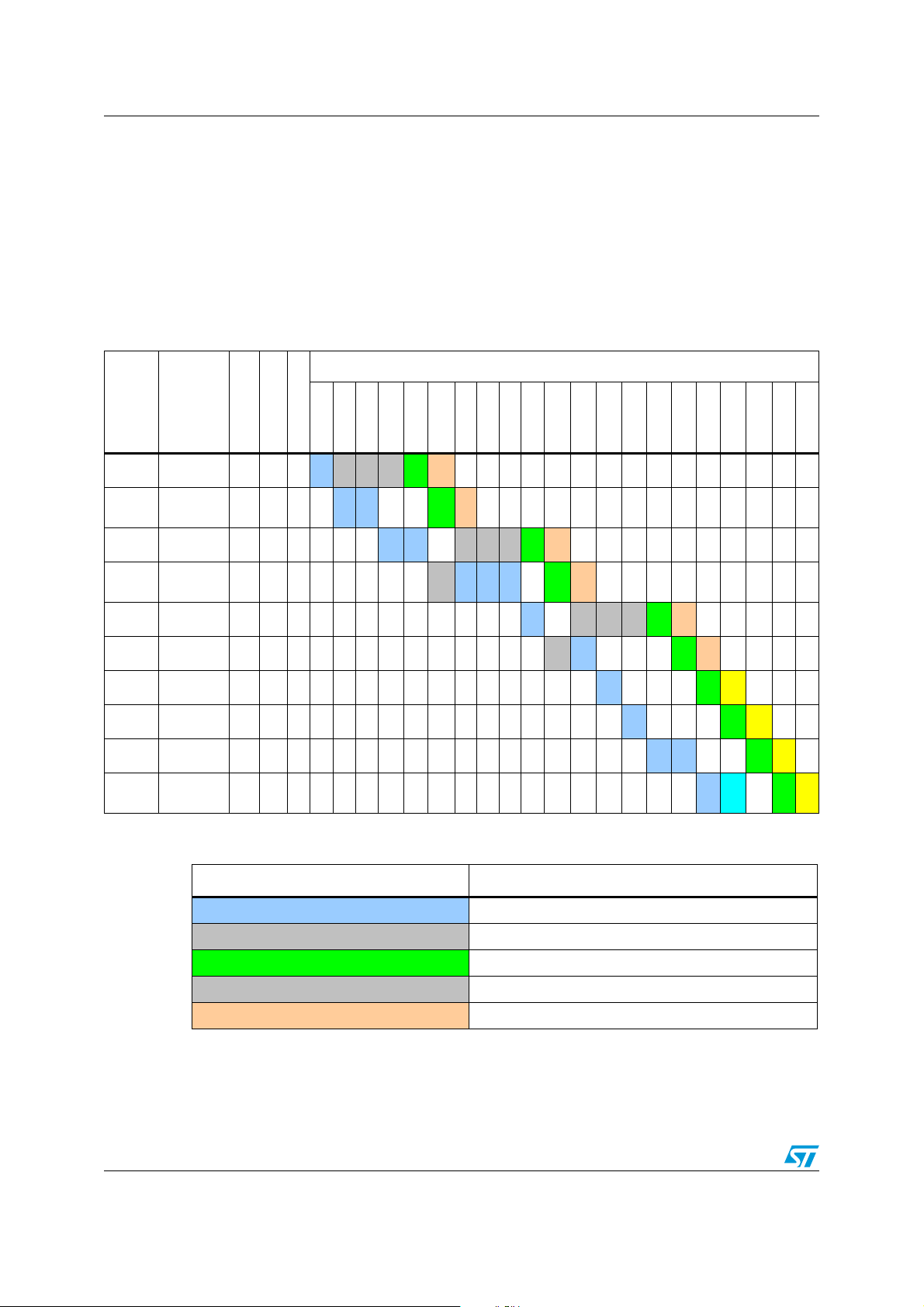
5.4.3 Pipeline with Call/Jump
In the example shown in Tab l e 1 0, a branch is taken after the JP/CALL instruction, and the
fetched instruction(s) are lost (flush). New instructions must be fetched. 3 fetch sequences
are required to refill the pre-fetch buffer. The fetch start depends on the instruction being
executed.
For a JP instruction, the fetch can start during the first cycle of the "dummy" execution.
For the CALL instruction, it starts after the last cycle of the CALL execution.
Table 10. Example of pipeline with Call/Jump
Cycle
D E
D E E
F
2
Add. Instruction
Decode
cycles
Execute
cycles
lgth
0xC000 INC A 1 1 1
0xC001 JP label 1 1 3
0xC004 LDW X,[$5432.w] X X 4
0xD010 label: NEG A 1 1 1
0xD011 CALL label2 1 2 3
0xD014 LDW X,[$5432.w] X X 4
1 23456 7 8 91011
D E
F
1
D E
F
2
Flush
F
1
0xD018 LDW X,[$7895.w] X X 4 F3FS
0xE030 label2: INCW X 1 1 1
Table 11. Legend
Symbol/Color Definition
FFetch
FS Fetch stalled
DDecode
EExecute
Flush
F1D E
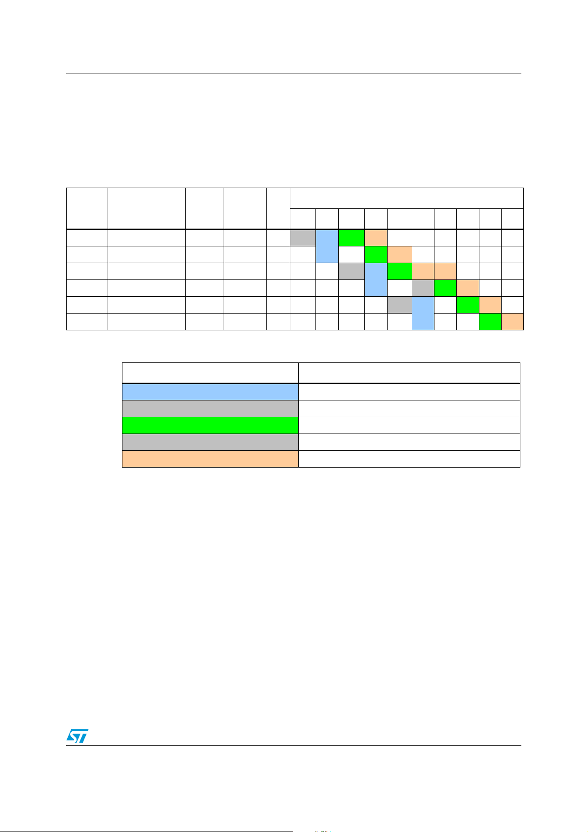
5.4.4 Pipeline stalled
The decode stage can be stalled when the execution lasts more than one cycle.
The flush is due to the branch. Fetching the branch address is performed during the second
execution cycle of the BTJF instruction.
The Decode operation can also be stalled when the memory target is modified during the
previous instruction. In the example given in Ta bl e 1 2, the INCW Y instruction writes the X
Doc ID 13590 Rev 3 27/162
Page 28
Pipelined execution PM0044
register during the first execution cycle. As a result, in this cycle, the next instruction
(LD A,(X)) cannot be decoded since it reads the X register.
Table 12. Example of stalled pipeline
Time (cycles)
D E E
D D E
Address Instruction
Decode
cycles
Execute
cycles
0xC000 SUB SP, #20 1 1 2
0xC002 LD A, #20 1 1 2
0xC004 BTJT 0x10, #5, to 1 2 5
0xC009 INC A 1 1 1
lgth
1 2347 8 91011121314
D E
F
1
D E
F
2
F
3
0xC00A BTJF 0x20, #3, to 1 2 5
F
0xC00F NOP X X 1
0xC010 LDW X,[$5432.w] X X 4 F
1
2
0xC014 LDW X,[$1234.w] X X 4 F
0xD020 to: INCW Y 1 1 2
0xD023 LD A,(X) 1 1 2
Table 13. Legend
Symbol/Color Definition
FFetch
D Decode stalled
D E E
3
Flush
F
D E
1
D D E
DDecode
EExecute
28/162 Doc ID 13590 Rev 3
Page 29
PM0044 Pipelined execution
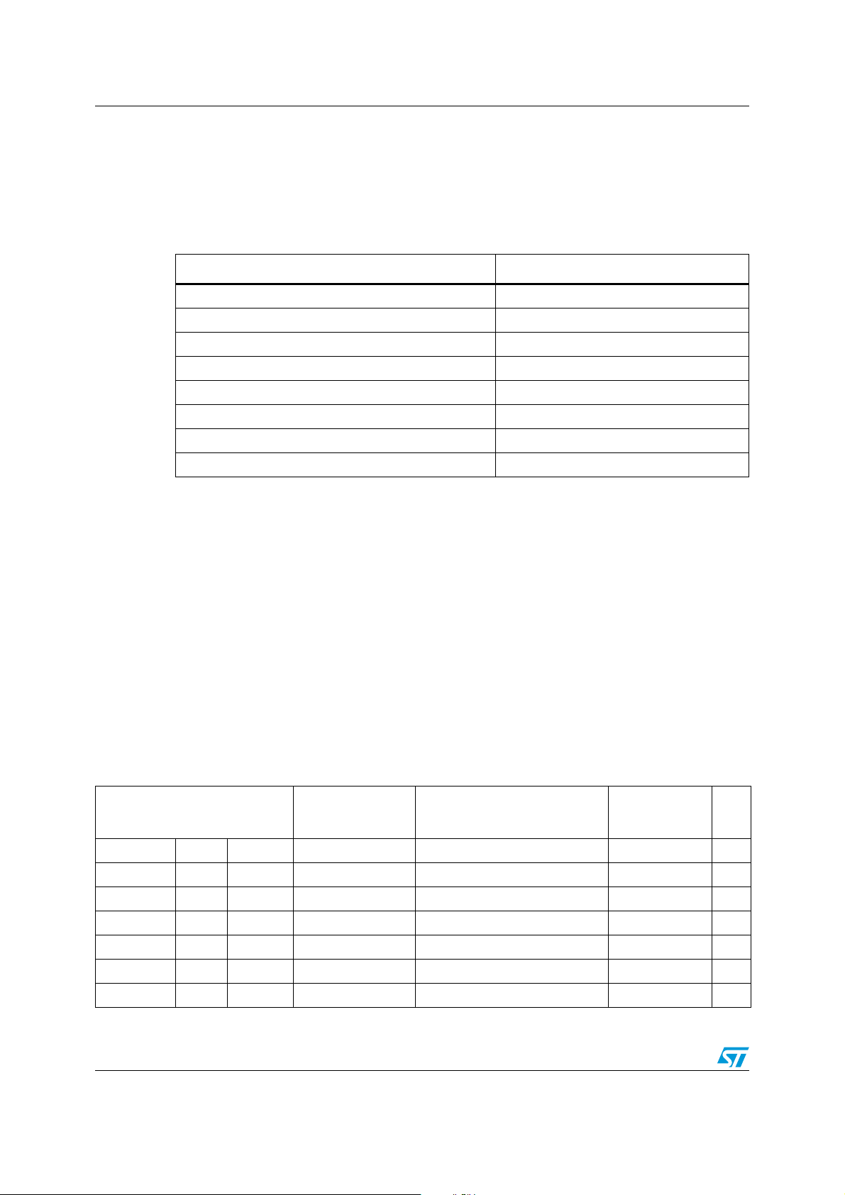
5.4.5 Pipeline with 1 wait state
In the example given in Ta bl e 1 4 , performing the fetch takes 2 cycles, and there is no
overlap between the 2 fetch cycles.
If the instruction is decoded/executed during the last 2 fetch cycles, then the wait state is
transparent compared to the no-wait state execution.
Table 14. Pipeline with 1 wait state
Address Instruction
Decode
cycles
Execute
cycles
0xC000 NEG A 1 1 1
0xC001 DEC ($10, X) 1 1 3
0xC004 LDW X, #20 1 1 3
0xC007 LD (X), A 1 1 1
0xC008 INC A 1 1 1
0xC009 NEG ($5A, Y) 1 1 1
Table 15. Legend
Symbol/Color Definition
FFetch
D Decode stalled
DDecode
MS Memory stalled
EExecute
lgth
Time (cycle)
12345678910
MS
D E
F
1
MS
D E
F
2
D E E
D D E
MS
F
3
D E
D E
Doc ID 13590 Rev 3 29/162
Page 30
STM8 addressing modes PM0044
6 STM8 addressing modes
The STM8 core features 18 different addressing modes which can be classified in 8 main
groups:
Table 16. STM8 core addressing modes
Addressing mode groups Example
Inherent NOP
Immediate LD A,#$55
Direct LD A,$55
Indexed LD A,($55,X)
SP Indexed LD A,($55,SP)
Indirect LD A,([$55],X)
Relative JRNE loop
Bit operation BSET byte,#5
The STM8 Instruction set is designed to minimize the number of required bytes per
instruction. To do so, most of the addressing modes can be split in three sub-modes called
extended, long and short:
● The extended addressing mode ("e") can reach any byte in the 16-Mbyte addressing
space, but the instruction size is bigger than the short and long addressing mode.
Moreover, the number of instructions with this addressing mode (far) is limited (CALLF,
RETF, JPF and LDF)
● The long addressing mode ("w") is the most powerful for program management, when
the program is executed in the same section (same PCE value). The long addressing
mode is optimized for data management in the first 64-Kbyte addressing space (from
0x000000 to 0x00FFFF) with a complete set of instructions, but the instruction size is
bigger than the short addressing mode.
● The short addressing mode ("b") is less powerful because it can only access the page
zero (from 0x000000 to 0x0000FF), but the instruction size is more compact.
Table 17. STM8 addressing mode overview
Inherent NOP
Immediate LD A,#$55
Short Direct LD A,$10 000000..0000FF
Long Direct LD A,$1000 000000..00FFFF
Extended Direct LDF A,$100000 000000..FFFFFF
Mode Syntax
Destination
address
Pointer
address
size
Pointer
No Offset Direct Indexed LD A,(X) 000000..00FFFF
Short Direct Indexed LD A,($10,X) 000000..0100FE
30/162 Doc ID 13590 Rev 3
Page 31
PM0044 STM8 addressing modes
Table 17. STM8 addressing mode overview (continued)
Mode Syntax
Short Direct
Long Direct Indexed LD A,($1000,X) 000000..01FFFE
Extended Direct Indexed LDF A,($100000,X) 000000..FFFFFF
Short
Pointer Long
Long Pointer
Long
Long Pointer
Extended
Short
Pointer Long
Long Pointer
Long
Long Pointer
Extended
Relative Direct JRNE loop PC+127/-128
Bit
Bit
Indirect LD A,[$10.w] 000000..00FFFF 000000..0000FF 2
indirect LD A,[$1000.w] 000000..00FFFF 000000..00FFFF 2
indirect LDF A,[$1000.e] 000000..FFFFFF 000000..00FFFF 3
Indirect Indexed LD A,([$10.w],X) 000000..01FFFE 000000..0000FF 2
Indirect
Indirect Indexed LDF A,([$1000.e],X) 000000..FFFFFF 000000..00FFFF 3
Long
Direct
Long
Direct
SP
Indexed
Indexed
(X only)
Relative BTJT $1000,#7,skip 000000..00FFFF PC+127/-128
LD A,($10,SP) 00..(FF+Stacktop)
LD A,([$1000.w],X) 000000..01FFFE 000000..00FFFF 2
BSET $1000,#7 000000..00FFFF
Destination
address
Pointer
address
size
Pointer
Doc ID 13590 Rev 3 31/162
Page 32

STM8 addressing modes PM0044
6.1 Inherent addressing mode
All related instructions are 1 or 2 byte. The op-code fully specifies all required information for
the CPU to process the operation.
Table 18. Inherent addressing instructions
Instructions Functions
NOP No operation
TRAP S/W Interrupt
WFI, WFE Wait For Interrupt / Event (Low Power Mode)
HALT Halt Oscillator (Lowest Power Mode)
RET Sub-routine Return
RETF Far Sub-routine Return
IRET Interrupt Sub-routine Return
SIM Set Interrupt Mask
RIM Reset Interrupt Mask
SCF Set Carry Flag
RCF Reset Carry Flag
RVF Reset Overflow Flag
CCF Complement Carry Flag
LD, LDW Load
CLR, CLRW Clear
PUSH, POP, PUSHW, POPW Push/Pop to/from the stack
INC, DEC, INCW, DECW Increment/Decrement
TNZ, TNZW Test Negative or Zero
CPL, NEG, CPLW, NEGW 1’s or 2’s Complement
MUL Byte Multiplication
DIV, DIVW Division
EXG, EXGW Exchange
SLA, SLL, SRL, SRA, RLC,
RRC, SLAW, SLLW, SRLW,
SRAW, RLCW, RRCW
SWAP, SWAPW Swap Nibbles/Bytes
Shift and Rotate Operations
Example:
1000 98 RCF ; Reset carry flag
1001 9D NOP ; No operation
1002 9F LD A,X; Transfer X register content into accumulator
1004 88 PUSH A; Push accumulator content onto the stack
32/162 Doc ID 13590 Rev 3
Page 33

PM0044 STM8 addressing modes
6.2 Immediate addressing mode
The data byte required for the operation, follows the op-code.
Table 19. Immediate addressing instructions
Instructions Functions
LD, MOV, LDW Load and move operation
CP, CPW Compare
BCP Bit Compare
AND, OR, XOR Logical Operations
ADC, ADD, SUB, SBC, ADDW, SUBW Arithmetic Operations
PUSH Stack Operations
These are two byte instructions, one for the op-code and the other one for the immediate
data byte.
Example:
05BA AEFF LD X,#$FF
05BC A355 CP X,#$55
05BE A6F8 LD A,#$F8
Action:
Load X = $FF
Compare (X, $55)
A = $F8
Doc ID 13590 Rev 3 33/162
Page 34

STM8 addressing modes PM0044
Previous Value
05BE
A
PC
A6
F8
Steps to Determine
Effective Address
PC = 05BE
PC = PC + 1 = 05BF
EA = PC = 05BF
New PC = PC + 1
= 05C0
Before Completion
F8
05C0
A
New PC
A6
F8
Instruction Complete
A = (EA) = F8
New PC = 05C
0
After Completion
LD A, #0F8h
05BE
05BF
05C0
05BE
05BF
05C0
VR02059A
Figure 7. Immediate addressing mode example
6.3 Direct addressing mode (Short, Long, Extended)
Table 20. Overview of Direct addressing mode instructions
Addressing mode Syntax EA formula Ptr Adr Ptr Size Dest adr
Short Direct shortmem (shortmem) op + 1 Byte 00..FF
Long Direct longmem (longmem) op + 1..2 Word 0000..FFFF
Extended Direct extmem (extmem) op + 1..3 Ext word 000000..FFFFFF
The data byte required for the operation is found by its memory address, which follows the
op-code.
Direct addressing mode is made of three sub-modes:
Table 21. Available Long and Short Direct addressing mode instructions
ADC, ADD, SUB, SBC, ADDW, SUBW Arithmetic Addition/Subtraction operations
Instructions Functions
LD, LDW Load
CP Compare
AND, OR, XOR Logical Operations
BCP Bit Compare
34/162 Doc ID 13590 Rev 3
Page 35

PM0044 STM8 addressing modes
Table 21. Available Long and Short Direct addressing mode instructions
Instructions Functions
MOV Move
CLR Clear
INC, DEC Increment/Decrement
TNZ Test Negative or Zero
CPL, NEG 1’s or 2’s Complement
SLA, SLL, SRL, SRA, RLC, RRC Shift and Rotate Operations
SWAP Swap Nibbles
CALL, JP Call or Jump subroutine
Table 22. Available Extended Direct addressing mode instructions
Instructions Function
CALLF, JPF Call or Jump FAR subroutine
LDF Far load
Table 23. Available Long Direct addressing mode instructions
Instructions Function
EXG Exchange
PUSH, POP Stack operation
Doc ID 13590 Rev 3 35/162
Page 36

STM8 addressing modes PM0044
Steps to Determine
Effective Address
PC = 052D
PC = PC + 1 = 052E
EA
Before Completion
Instruction Complete
A = (EA) = 20
New PC = 052F
After Completion
= (PC)
= (4B + 0000)
= 004
B
20
B6
4B
LD A,Coeff
A
004BEA
052D
P
C
Previous Valu
e
A
20
052F
New P
C
004B
052D
052E
052F
Coeff .byte 20h
VR02059
L
20
B6
4
B
004B
052D
052E
052
F
Coeff .byte 20h
LD A,Coeff
PC + 1
=
6.3.1 Short Direct addressing mode
The address is a byte, thus require only one byte after the op-code, but only allow 00..FF
addressing space.
Example:
004B 20 coeff dc.b $20
052D B64B LD A,coeff
Action:
A = (coeff) = ($4B) = $20
Figure 8. Short Direct addressing mode example
36/162 Doc ID 13590 Rev 3
Page 37

PM0044 STM8 addressing modes
Previous Value
0409
A
PC
E5
Steps to Determine
Effective Address
PC = 0409
PC = PC + 1 = 040A
EA = (PC) : (PC+1) = 06E5
PC + 2 =
Before Completion
40
040C
A
New PC
Instruction Complete
A = (EA) = 40
New PC = 040C
After Completion
C6
06E5E
A
06
4
0
06E5
E5
C
6
06
4
0
040A
040B
040C
040A
040B
040C
0409
0409
06E5
06E
5
VR02059
B
LD A,Coeff
LD A,Coeff
Coeff .byte 040h
Coeff .byte 040h
6.3.2 Long Direct addressing mode
The address is a word, thus allowing 0000 to FFFF addressing space, but requires 2 bytes
after the op-code.
Example:
0409 C606E5 LD A,coeff
06E5 40 coeff dc.b $ 40
Action:
A = (coeff) = ($06E5) = $40
Figure 9. Long Direct addressing mode example
Doc ID 13590 Rev 3 37/162
Page 38

STM8 addressing modes PM0044
Previous Value
0409
A
PC
06
Steps to Determine
Effective Address
PC = 0409
New PC =
Before Completion
New PC
Instruction Complete
New PC =
After Completion
8D
E
A
01
06
8D
01
4C
040A
040B
040C
040A
040B
040C
0409
0409
VR02059U
INC A
CALLF
sw_routine
CALLF
sw_routine
0106E5
0106E5
0106E5
0106E5
4C
E5
INC A
0106E5
0106E5
EA
E5
PC=PC+1
EA=(PC):(PC+1):(PC+2)
=0106E5
6.3.3 Extended Direct addressing mode (only for CALLF and JPF)
The address is an extended word, thus allowing 000000 to FFFFFF addressing space, but
requires 3 bytes after the op-code.
Example:
000409 8D0106E5 CALLF sw_routine
0106E5 4C sw_routine INC A
Action:
PC = $0106E5
Figure 10. Far Direct addressing mode example
38/162 Doc ID 13590 Rev 3
Page 39

PM0044 STM8 addressing modes
6.4 Indexed addressing mode (No Offset, Short, SP, Long, Extended)
Table 24. Overview Indexed addressing mode instructions
Addressing mode Syntax EA formula Ptr Adr Ptr Size Dest adr
No offset Direct Indexed (ndx) (ndx) --- --- 00..FFFF
Short Direct Indexed (shortoff,ndx) (ptr + ndx) op + 1 Byte 00..100FE
Stack
Pointer
Long Direct Indexed (longoff,ndx) (ptr.w + ndx) op + 1..2 Word 000000..01FFFE
Extended Direct Indexed (extoff,ndx) (ptr.e + ndx) op + 1..3 Ext Word 000000..FFFFFF
The data byte required for operation is found by its memory address, which is defined by the
unsigned addition of an index register (X or Y or SP) with an offset which follows the opcode.
The indexed addressing mode is made of five sub-modes:
Table 25. No Offset, Long, Short and SP Indexed instructions
Direct Indexed (shortoff,SP) (ptr + SP) op + 1 Byte 00..(FF+stacktop)
Instructions Functions
LD, LDW Load
CLR Clear
CP Compare
AND, OR, XOR Logical Operations
ADC, ADD, SUB, SBC, ADDW, SUBW Arithmetic Addition/Subtraction operations
INC, DEC Increment/Decrement
TNZ Test Negative or Zero
CPL, NEG 1’s or 2’s Complement
SLA, SLL, SRL, SRA, RLC, RRC Shift and Rotate Operations
SWAP Swap Nibbles
Table 26. No Offset, Long, Short Indexed Instructions
Instructions Functions
CALL, JP Call or Jump subroutine
Table 27. Extended Indexed Instructions only
Instructions Functions
LDF Far Load
Doc ID 13590 Rev 3 39/162
Page 40

STM8 addressing modes PM0044
Previous Value
B8
A
X
Steps to determine
Effective Address
PC = 05F4
EA = X + 0000 = 00B8
Before completion
Instruction Complete
A = (EA) = 11
New PC = PC +1 = 05F5
After completion
00B8
F6
05F4
EA
PC
11
A
11
X
B8
New PC
05F5
LD A,(X)
Table .word 1122
00B8
05F4
05F4
05F5
00B8
VR02059C
44
33
22
F6
11
44
33
22
Table .word 1122
LD A,(X)
00B9
00BA
00BB
6.4.1 No Offset Indexed addressing mode
There is no offset, (no extra byte after the op-code), but only allows 00..FF addressing
space.
Example:
00B8 11223344 table dc.w $1122, $3344
05F2 AEB8 LD X,#table
05F4 F6 LD A,(X)
Action:
X = table
A = (X) = (table) = ($B8) = $11
Figure 11. No Offset Indexed addressing mode example
40/162 Doc ID 13590 Rev 3
Page 41

PM0044 STM8 addressing modes
Previous Value
03
A
X
Steps to determine
Effective Address
PC = 075B
PC = PC + 1 = 075C
EA = (PC) + X = 89 + 03 = 008C
Before completion
Instruction Complete
A = (EA) = 44
New PC = PC + 1 = 075D
After Completion
008C
075B
PC
A
44
X
03
New PC
075D
11
22
33
44
E6
89
E6
89
Adder
EA
075B
075B
0089
008A
008B
008C
075C
075D
0089
008A
008B
008C
075C
075D
LD A, (table,X)
LD A, (table,X)
VR02059D
Table .long 11223344
Table .long 11223344
11
22
33
44
89
03
6.4.2 Short Indexed addressing mode
The offset is a byte, thus requires only one byte after the op-code, but only allows 00..1FE
addressing space.
Example:
0089 11223344 table dc.l
0759 AE03 LD
075B E689 LD A,(table,X)
Action:
X = 3
A = (table, X) = ($89, X) = ($89, 3) = ($8C) = $44
Figure 12. Short Indexed - 8-bit offset - addressing mode example
$11223344
X,#3
Doc ID 13590 Rev 3 41/162
Page 42

STM8 addressing modes PM0044
Previous Value
A
Steps to determine
effective address
PC = 0089
PC = PC + 1 = 008A
EA = (PC) + SP=03+1FFC= 1FFF
Before completion
Instruction Complete
A = (EA) = 11
New PC = PC+1 = 008B
After completion
1FFF
1FFC
SP
A
11
SP
1FFC
New PC
008B
7B
03
33
22
Adder
EA
1FFD
0089
008A
008B
1FFE
1FFF
LD A, ($03,SP)
VR02059D
1FFC
11
PC
0089
1FFC 03
7B
03
33
22
1FFD
0089
008A
008B
1FFE
1FFF
LD A, ($03,SP)
1FFC
11
6.4.3 SP Indexed addressing mode
The offset is a byte, thus require only one byte after the op-code, but only allow 00..(FF +
stack top) addressing space.
Example:
0086 4B11 PUSH #$11
0087 4B22 PUSH #$22
0088 4B33 PUSH #$33
0089 7B03 LD A,($03,SP)
Action:
A = ($03, SP) = ($03, $1FFC) = ($1FFF) = $11
Figure 13. SP Indexed - 8-bit offset - addressing mode example
42/162 Doc ID 13590 Rev 3
Page 43

PM0044 STM8 addressing modes
0692
02
PC
X
Steps to Determine
Effective Address
PC = 0692
PC = PC + 1 = 0693
EA = (PC):(PC+1) + X
Before completion
Instruction Complete
A = (EA) = DB
New PC = PC + 2 = 0695
After Completion
0780
Previous Value
A
X
02
0695
A
DB
D6
07
7E
86
DB
Adder
EA
table . byte BF
BF
CF
= 077E + 02 = 0780
D6
07
7E
86
DB
table . byte BF BF
CF
New PC
LD A, (table, X)
LD A, (table, X)
0693
0694
077F
0780
0781
0694
077E
077F
0780
0781
0693
0695
0692
0692
077E
VR02059E
077E 02
6.4.4 Long Indexed addressing mode
The offset is a word, thus allowing up to 128 KB addressing space, but requires 2 bytes after
the op-code.
Example:
0690 AE02 LD X,#2
0692 D6077E LD A,(table,X)
077E BF table dc.b $BF
86 dc.b $86
DBCF dc.w $DBCF
Action:
X = 2
A = (table, X) = ($077E, X) = ($077E, 2) = ($0780) = $DB
Figure 14. Long Indexed - 16-bit offset - addressing mode example
Doc ID 13590 Rev 3 43/162
Page 44

STM8 addressing modes PM0044
0692
02
PC
X
Steps to determine
Effective Address
PC = 0692
PC = PC + 1 = 0693
EA= (PC):(PC+1):(PC+2)+X
Before Completion
Instruction Complete
A = (EA) = DD
New PC = PC+3 = 0696
After Completion
010782
Previous Value
A
X
02
0696
A
DD
AF
01
07
86
Adder
EA
table . byte BF
BF
= 010780+02 = 010782
AF
01
07
86
DD
table . byte BF
BF
FE
New PC
LDF A, (table, X)
LD A, (table, X)
0693
0694
010780
010781
0694
010780
010781
0693
0695
0692
0692
VR02059R
80
DD
FE 010783
010782
0695
80
010782
010783
0696
010780 02
6.4.5 Extended Indexed (only LDF instruction)
The offset is an extended word, thus allowing 16Mbyte addressing space (from 000000 to
FFFFFF), but requires 3 bytes after the op-code.
Example:
0690 AE02 LD X,#2
0692 AF010780 LDF A,(table,X)
010780 BF table dc.b $BF
86 dc.b $86
DDFE dc.w $DDFE
Action:
Figure 15. Far Indexed - 16-bit offset - addressing mode example
X = 2, A = (table, X) = ($010780,X) = ($010780+2)) = ($010782) = $DD
44/162 Doc ID 13590 Rev 3
Page 45
PM0044 STM8 addressing modes
6.5 Indirect (Short Pointer Long, Long Pointer Long)
Table 28. Overview of Indirect addressing instructions
Addressing mode Syntax EA formula Ptr Adr
Ptr
Size
Dest adr
Short Pointer Long Indirect ((shortptr.w)) ((shortptr.w)) 00..FF Word 0000..FFFF
Long Pointer Long Indirect ((longptr.w)) ((longptr.w)) 0000..FFFF Word 0000..FFFF
The data byte required for the operation is found by its memory address, located in memory
(pointer).
The pointer address follows the op-code. The indirect addressing mode is made of three
sub-modes:
Table 29. Available Long Pointer Long and Short Pointer Long Indirect Instructions
Instructions Functions
LD, LDW Load
CP Compare
AND, OR, XOR Logical Operations
ADC, ADD, SUB, SBC Arithmetic Addition/Subtraction operations
BCP Bit Compare
CALL, JP Call or Jump subroutine
Table 30. Available Long Pointer Long Indirect Instructions
Instructions Functions
CLR Clear
TNZ Test Negative or Zero
CPL, NEG 1’s or 2’s Complement
SLA, SLL, SRL, SRA, RLC, RRC Shift and Rotate Operations
SWAP Swap Nibbles
INC, DEC Increment/Decrement
Doc ID 13590 Rev 3 45/162
Page 46

STM8 addressing modes PM0044
Steps to determine
Effective Address
PC = 0409
PC = PC + 2 = 40B
EA
Before Completion
Instruction Complete
New PC = PC +1 = 040C
After Completion
= ((PC)) :((PC)+1)
= 42E5
A
PC
Previous Value
92
42
E5
C6
40
ptr .word var
0409
040A
040B
040C
0409
EA 42E5
42E5
11
92
42
E5
C6
40
ptr .word var
0409
040A
040B
040C
42E5
11
A
040C
New PC
0040
0041
0040
0041
A = (EA) = 0x11
var.byte 0x011
var .byte 0x011
0x11
LD A, [shortptr.w]
LD A, [shortptr.w]
6.6 Short Pointer Indirect Long addressing mode
The pointer address is a byte, the pointer size is a word, thus allowing up to 128 KB
addressing space, and requires 1 byte after the op-code.
Example:
0040 42E5 ptr dc.w var
0409 92C640 LD A,[shortptr.w]
42E5 11 var dc.b $11
Action:
A = [shortptr.w] = ((shortptr.w)) = (($40.w)) = ($42E5) =
$11
Figure 16. Short Pointer Indirect Long addressing mode example
46/162 Doc ID 13590 Rev 3
Page 47
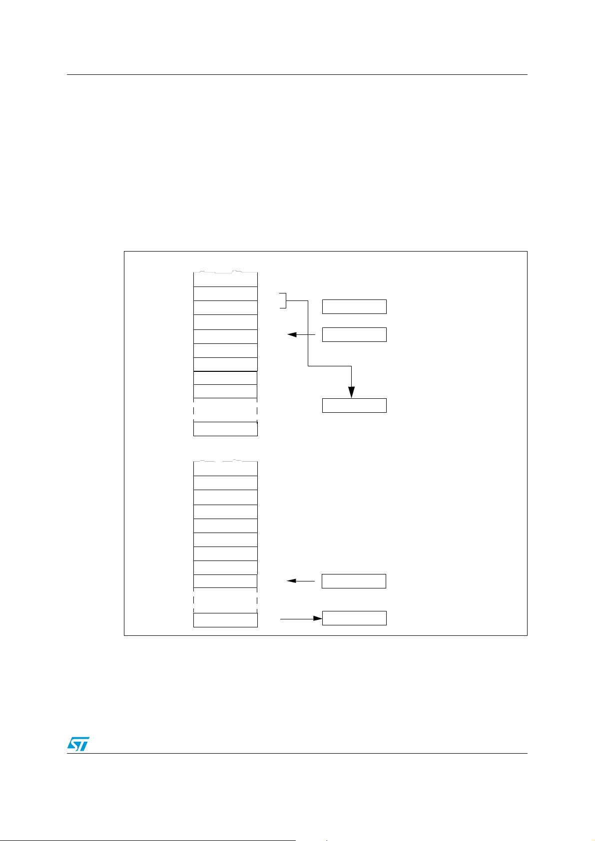
PM0044 STM8 addressing modes
Steps to determine
Effective Address
PC = 1409
PC = PC + 2 = 140B
EA
Before Completion
Instruction complete
New PC = PC + 2 = 140D
After Completion
=((PC):(PC+1)):
A
PC
Previous Value
72
42
E5
C6
10
ptr .word var
1409
140A
140B
140C
1409
EA 42E5
42E5
11
72
42
E5
C6
10
ptr .word var
1409
140A
140B
140C
42E5
11
A
040D
New PC
1040
1041
1040
1041
A = (EA) = 0x11
var.byte 0x011
var .byte 0x11
0x11
LD A, [longptr.w]
LD A, [longptr.w]
VR02059G
40
140D
40
140D
((PC):(PC+1)+1)
= 42E5
6.7 Long Pointer Indirect Long addressing mode
The pointer address is a word, the pointer size is a word, thus allowing 64 KB addressing
space, and requires 2 bytes after the op-code.
Example:
1040 42E5 ptr dc.w var
1409 72C61040 LD A,[longptr.w]
42E5 11 var dc.b $11
Action:
A = [longptr.w] = ((longptr.w)) = (($1040.w)) = ($42E5) = $11
Figure 17. Long Pointer Indirect Long addressing mode example
Doc ID 13590 Rev 3 47/162
Page 48

STM8 addressing modes PM0044
6.8 Indirect Indexed (Short Pointer Long, Long Pointer Long, Long Pointer Extended) addressing mode
Table 31. Overview of Indirect indexed instructions
Addressing mode Syntax EA formula Ptr Adr Ptr Size Dest adr
Short Pointer
Long
Long Pointer
Long
Long Pointer
Extended
Indirect Indexed ([shortptr.w],ndx) ((shortptr.w) + ndx) 00..FF Word 000000.01FFFE
Indirect Indexed ([longptr.w],ndx) ([longptr.w] +ndx) 00..FFFF Word 000000.01FFFE
Indirect Indexed ([longptr.e],ndx) ([longptr.e] +ndx) 00..FFFF Extword 000000.FFFFFE
This is a combination of indirect and indexed addressing mode. The data byte required for
the operation is found by its memory address, which is defined by the unsigned addition of
an index register value (X or Y) with a pointer value located in memory. The pointer address
follows the op-code.
The indirect indexed addressing mode is made of four sub-modes:
Table 32. Available Long Pointer Long and Short Pointer Long Indirect
Indexed instructions
Instructions Functions
LD, LDW Load
CP Compare
AND, OR, XOR Logical Operations
ADC, ADD, SUB, SBC Arithmetic Addition/Subtraction operations
BCP Bit Compare
CALL, JP Call or Jump subroutine
Table 33. Available Long Pointer Long Indirect Indexed instructions
Instructions Functions
CLR Clear
TNZ Test Negative or Zero
CPL, NEG 1’s or 2’s Complement
SLA,SLL, SRL, SRA, RLC, RRC Shift and Rotate Operations
SWAP Swap Nibbles
INC, DEC Increment/Decrement
Table 34. Long Pointer Extended Indirect Indexed instructions instruction
Instructions Functions
LDF Far load
48/162 Doc ID 13590 Rev 3
Page 49

PM0044 STM8 addressing modes
6.9 Short Pointer Indirect Long Indexed addressing mode
The pointer address is a byte, the pointer size is a word, thus allowing up to 128 KB
addressing space, and requires 1 byte after the op-code.
Example:
0089 0800 ptr dc.w table
0800 10203040 table dc.b $10,$20,$30,$40
0690 AE03 LD X,#3
0692 92D689 LD A,([shortptr.w],X)
X = 3
A = ([shortptr.w],X) = ((shortptr.w), X)
= (($89.w), 3)
= ($0800,3) = ($0803) = $40
Doc ID 13590 Rev 3 49/162
Page 50

STM8 addressing modes PM0044
Steps to determine
Effective Address
PC = 0692
PC = PC + 2 = 0694
EA = ((PC)) : ((PC)+1) + X
Before completion
Instruction Complete
A = (EA) = 40
New PC = PC + 1 = 0695
After completion
EA = 0803
08
00
92
D6
89
10
20
30
40
PC
0692
X
03
A
Previous value
Adder
EA
0803
ptr .word table
08
00
92
D6
89
10
20
30
40
ptr .word table
X
03
New PC
0695
A
40
800
03
table .byte 0x10,
0x20,0x30
table .byte
0x10,0x20,0x30,
0089
008A
0692
0693
0694
800
801
802
803
0089
008A
0692
0693
0694
0800
0801
0802
0803
0695
LD A,([shortptr.w],X)
LD A,([shortptr.w],X)
0x40
0x40
Figure 18. Short Pointer Indirect Long Indexed addressing mode example
50/162 Doc ID 13590 Rev 3
Page 51

PM0044 STM8 addressing modes
6.10 Long Pointer Indirect Long Indexed addressing mode
The pointer address is a word, the pointer size is a word, thus allowing up to 128 KB
addressing space, and requires 2 bytes after the op-code.
Example:
1089 1800 ptr dc.w table
1800 10203040 table dc.b $10,$20,$30,$40
1690 AE03 LD X,#3
1692 72D61089 LD A,([longptr.w],X)
X = 3
A = ([longptr.w],X) = ((longptr.w), X) =
(($1089.w), 3)
= ($1800,3) = ($1803) = $40
Doc ID 13590 Rev 3 51/162
Page 52

STM8 addressing modes PM0044
Steps to determine
Effective Address
PC = 1692
PC = PC + 2 = 1694
EA = (((PC) : (PC+1)) :
Before completion
Instruction Complete
A = (EA) = 40
New PC = PC + 2 = 1696
After completion
18
00
72
D6
89
10
20
30
40
PC
1692
X
03
A
Previous value
Adder
EA
1803
ptr .word table
18
00
92
D6
10
10
20
30
40
ptr .word table
X
03
New PC
1696
A
40
1800
03
table .byte
0x10,0x20,0x30,
table .byte
0x10,0x20,0x30,
1089
108A
1692
1693
1694
1800
1801
1802
1803
1089
108A
1692
1693
1694
1800
1801
1802
1803
1695
LD A,([longptr.w],X)
1695
10
89
1696
EA = 1803
((PC) : (PC+1) +1)) + X
LD A,([longptr.w],X)
0x40
0x40
Figure 19. Long Pointer Indirect Long Indexed addressing mode example
52/162 Doc ID 13590 Rev 3
Page 53

PM0044 STM8 addressing modes
6.11 Long Pointer Indirect Extended Indexed addressing mode
The pointer address is a word, the pointer size is an extended word, thus allowing 16-Mbyte
addressing space, and requires 2 bytes after the op-code.
Example:
1089 180000 ptr dc.b page(table), high(table), low(table)
180000 10203040 table dc.b $10,$20,$30,$40
1690 AE03 LD X,#3
1692 72A71089 LDF A,([longptr.e],X)
X = 3
A = ([longptr.e],X) = ((longptr.e), X) =
(($1089.e), 3)
= ($180000,3) = ($180003) = $40
Doc ID 13590 Rev 3 53/162
Page 54

STM8 addressing modes PM0044
Steps to Determine
Effective Address
PC = 1692
PC = PC + 2 = 1694
EA = (((PC) : (PC+1)) :
Before completion
Instruction Complete
A = (EA) = 40
New PC = PC + 2 = 1696
After completion
18
00
72
A7
89
10
20
30
40
PC
1692
X
03
A
Previous value
Adder
EA
180003
ptr .word table
18
00
72
A7
10
10
20
30
40
ptr .word table
X
03
New PC
1696
A
40
180000
03
table .byte
0x10,0x20,0x30,
table .byte
0x10,0x20,0x30,
108A
108B
1692
1693
1694
180000
180001
180002
180003
1089
108A
1692
1693
1694
180000
180001
180002
180003
1695
LDF A,([longptr.w],X)
VR02059I
1695
10
89
1696
EA = 180003
((PC) : (PC+1) +1) :
00
1089
00
108B
((PC) : (PC+1) +2)) + X
LDF A,([longptr.w],X)
0x40
0x40
Figure 20. Long Pointer Indirect Extended Indexed addressing mode example
54/162 Doc ID 13590 Rev 3
Page 55

PM0044 STM8 addressing modes
6.12 Relative Direct addressing mode
Table 35. Overview of Relative Direct addressing mode instructions
Addressing mode Syntax EA formula Ptr Adr Ptr Size Dest adr
Direct Relative off PC = PC + off op + 1 --- PC +127/-128
This addressing mode is used to modify the PC register value, by adding an 8-bit signed
offset to it. The offset added to the PC register value is relative to the start of the next
instruction.
Table 36. Available Relative Direct instructions
Instructions Functions
JRxx Conditional Jump
JRA Jump Relative Always
CALLR Call Relative
The offset follows the op-code.
Example:
04A7 2717 jreq skip
04A9 9D nop
04AA 9D nop
04C0 20FE skip jra* ; Infinite loop
Action:
if (Z == 1)then PC = PC + $17 = $04A9 + $17 = $04C0
elsePC = PC= $04A9
Doc ID 13590 Rev 3 55/162
Page 56

STM8 addressing modes PM0044
Z
CC
Before completion
After completion
Z = 1
04A9
27
17
Adder
27
17
PC
EA
(Branch taken)
CC
Adder
04C0
New PC
04A9
SKIP :
Instruction Complete
New PC = EA = 04C0
Steps to Determine
Effective Address
PC = 04A7
PC = PC + 1 = 04A8
TEMP = (PC) = 17
PC = PC +1 = 04A9
Stop here if there
is no Branch; i.e., Z = 0
EA = PC + TEMP
= 04A9 + 17
= 04C0
New PC = EA if Branch is taken
JREQ SKIP
JREQ SKIP
EA
02
PC
04A8
04A9
04A8
04C0
04A9
04A7
04A7
04A7
17
04C0
Z = 0
27
17
04A8
04A9
CC
04A9
New PC
Instruction Complete
New PC = EA = 04A9
JREQ SKIP
04A7
04A7
04A9
After completion
(No branch taken)
Figure 21. Relative Direct addressing mode example
56/162 Doc ID 13590 Rev 3
Page 57

PM0044 STM8 addressing modes
6.13 Bit Direct (Long) addressing mode
Table 37. Overview of Bit Direct addressing mode instruction
Addressing mode Syntax EA formula Ptr Adr Ptr Size Dest adr
Bit Long Direct longmem, #pos (longmem) op + 1..2 Word 0000..FFFF
The data byte required for the operation is found by its memory address, which follows the
op-code. The bit used for the operation is selected by the bit selector which is encoded in
the instruction op-code.
Table 38. Available Bit Direct instructions
Instructions Functions
BRES Bit Reset
BSET Bit Set
BCPL Bit Complement
BCCM Copy Carry Bit to Memory
The address is a word, thus allowing 0000 to FFFF addressing space, but requires 2 bytes
after the op-code. The bit selector #n (n=0 to 7) selects the n
th
bit from the byte pointed to by
the address.
Example:
0408 721006E5 BCPL coeff, #0
06E5 40 coeff dc.b $ 40
Action:
(coeff) = ($06E5) XOR 2**0 = $40 XOR $01 = $41
Doc ID 13590 Rev 3 57/162
Page 58

STM8 addressing modes PM0044
0408
PC
E5
Steps to determine
effective address
PC = 0408
PC = PC + 2 = 040A
EA = (PC ) : (PC+1) = 06E5
PC + 2 =
Before completion
40 XOR 01
040C
New PC
Instruction complete
New PC = 040C
After completion
10
06E5E
A
06
4
0
06E5
E5
10
06
4
1
040A
040B
040C
040A
040B
040C
0409
0409
06E5
06E
5
Coeff .byte 040h
Coeff .byte 040h
(EA) = (EA) | 2**0 = 40 | 01 = 41
90
0408BCPL Coeff,#0
90
0408BCPL Coeff,#0
EA = (PC ) : (PC+1) = 06E5
Figure 22. Bit Long Direct addressing mode example
58/162 Doc ID 13590 Rev 3
Page 59

PM0044 STM8 addressing modes
6.14 Bit Direct (Long) Relative addressing mode
Table 39. Overview of Bit Direct (Long) Relative addressing mode
Addressing mode Syntax EA formula Ptr Adr Ptr Size Dest adr
(longmem) op + 1..2 Word 0000..FFFF
PC = PC + off op + 3 Byte
PC +127/-
128
Bit
Long
Direct
Relative longmem, #pos, off
This addressing mode is a combination between the Bit Direct addressing mode (for data
addressing) and Relative Direct mode (for PC computation).
The data byte required for the operation is found by its memory address, which follows the
op-code. The bit used for the test operation is selected by the bit selector which is encoded
in the instruction op-code. Following the logical test operation, the PC register value can be
modified, by adding an 8-bit signed offset to it.
Table 40. Available Bit Direct Relative instructions
Instructions Functions
BTJT, BTJF Bit Test and Jump
The data address is a word, thus allowing 0000 to FFFF addressing space (requires 2 bytes
after the op-code). The bit selector #n (n=0 to 7) selects the n
th
bit from the byte pointed to
by the address. The offset follows the op-code and data address.
Example:
104B 00 DRA dc.b $00 ; Port A data
register (input
value)
bit0 equ $0 ; data bit 0
04A7 7201104BFB wait_1 BTJF DRA, bit0, wait_1
04AC .... cont_0
Action:
Test = select_bit(0, ($4B)) = select_bit(0, DRA)
if (Test /= 1) then PC = PC + $FB = $0004AC - $05 =
else PC = PC = $0004AC
Doc ID 13590 Rev 3 59/162
$0004A7
Page 60

STM8 addressing modes PM0044
After completion
b0 = 0
04AC
72
01
Adder
72
01
PC
EA
(Branch taken)
(EA)
Adder
04A7
New PC
04AC
Instruction Complete
New PC = EA = 04A7
Steps to Determine
Effective Address
PC = 04A7
PC = PC + 2 = 04A9
TEMP = (PC) = FC
PC = PC +1 = 04AC
Stop here if there
is no Branch; i.e., Test = TRUE (1)
EA = PC + TEMP
= 04AA + FD
= 04A7
New PC = EA if Branch is taken
wait_1
EA
05
PC
04A8
04A9
04A8
04A9
04A7
04A7
04A7
FB
04A7
b0 = 1
01
10
04A9
04AA
(EA)
04AC
New PC
Instruction Complete
New PC = EA = 04AC
04A8
04A7
04AC
After completion
(No branch taken)
DRA .byte
104C
104B
DRA
b0
BTJF DRA, #0, wait_1
DRA.b0 =? 0
10
EA = (PC):(PC+1) = 104B
PC = PC + 2 = 04AB
Test = (EA).b0
10
4B
04AB
wait_1
BTJF DRA, #0, wait_1
wait_1
BTJF DRA, #0, wait_1
04AA
4B
04AA
4B
04AC
FB
04AB
FB
04AB
FB
72
04A7
Figure 23. Bit Long Direct Relative addressing mode example
60/162 Doc ID 13590 Rev 3
Page 61
PM0044 STM8 instruction set
7 STM8 instruction set
7.1 Introduction
This chapter describes all the STM8 instructions. There are 96 and they are described in
alphabetical order. However, they can be classified in 13 main groups as follows:
Table 41. Instruction groups
Load and
Transfer
Stack
operation
LD
PUSH POP
LDF
CLR MOV EXG LDW CLRW EXGW
PUSH
W
POPW
Increment/
Decrement
Compare and
Tests
Logical
operations
Bit Operation BSET BRES BCPL BCCM
Conditional Bit
Test and
Branch
Arithmetic
operations
Shift and
Rotates
Unconditional
Jump or Call
Conditional
Branch/
Execution
Interrupt
management
Condition
Code Flag
modification
Breakpoint/
software break
INC DEC INCW DECW
CP TNZ BCP CPW TNZW
AND OR XOR CPL CPLW
BTJT BTJF
NEG ADC ADD SUB SBC MUL DIV DIVW NEGW ADDW SUBW
SLL SRL SRA RLC RRC SWAP SLLW SRLW SRAW RLCW RRCW
SWAP RLWA RRWA
JRA JRT JRF JP JPF CALL CALLR CALLF RET RETF NOP
JRxx WFE
TRAP WFI HALT IRET
SIM RIM SCF RCF CCF RVF
BREAK
The instructions are described with one to five bytes.
PC-1 End of previous instruction
PC Op-code
PC+1..4 Additional word (0 to 4) according to the number of bytes required to compute the
effective address(es)
Doc ID 13590 Rev 3 61/162
Page 62

STM8 instruction set PM0044
Using a pre-code (two-byte op-codes)
In order to extend the number of available op-codes for an 8-bit CPU (256 op-codes), four
different pre-code bytes are defined. These pre-codes modify the meaning of the instruction
they precede.
The whole instruction becomes:
PC-1 End of previous instruction
PC Pre-code
PC+1 Op-code
PC+2 Additional word (0 to 3) according to the number of bytes required to compute the
effective address
These pre-bytes are:
0x90 = PDY Replaces an X based instruction using immediate, direct, indexed or
inherent addressing mode by a Y one.
It also provides read/modify/write instructions using Y indexed
addressing mode with long offset and two bit handling instructions
(BCPL and BCCM)
0x92 = PIX Replaces an instruction using direct, direct bit, or direct relative
addressing mode to an instruction using the corresponding indirect
addressing mode.
It also changes an instruction using X indexed addressing mode to
an instruction using indirect X indexed addressing mode.
0x91 = PIY Replace an instruction using indirect X indexed addressing mode by
a Y one.
0x72 = PWSP Provide long addressing mode for bit handling and read/modify/write
instructions.
It also provides indirect addressing mode with two byte pointer for
read/modify/write and register/memory instructions.
Finally it provides stack pointer indexed addressing mode on
register/memory instructions.
62/162 Doc ID 13590 Rev 3
Page 63

PM0044 STM8 instruction set
7.2 Nomenclature
7.2.1 Operators
← is loaded with ...
↔ has its value exchanged with ...
7.2.2 CPU registers
A accumulator
X X index register (2 bytes)
XL least significant byte of the X index register (1 byte)
XH most significant byte of the X index register (1 byte)
Y Y index register (2 bytes)
YL least significant byte of the Y index register (1 byte)
YH most significant byte of the Y index register (1 byte)
PC program counter register (3 bytes)
PCL low significant byte of the program counter register (1 byte)
PCH high significant byte of the program counter register (1 byte)
PCE extended significant byte of the program counter register (1 byte)
SP stack pointer register (2 bytes)
CC Condition code register (1 byte)
CC.V overflow flag of the code condition register (1 bit)
CC.I0 interrupt mask bit 0 of the code condition register (1 bit)
CC.H half carry flag of the code condition register (1 bit)
CC.I1 interrupt mask bit 1 of the code condition register (1 bit)
CC.N negative flag of the code condition register (1 bit)
CC.Z zero flag of the code condition register (1 bit)
CC.C carry flag of the code condition register (1 bit)
7.2.3 Code condition bit value notation
- bit not affected by the instruction
1 bit forced to 1 by the instruction
0 bit forced to 0 by the instruction
X bit modified by the instruction
7.2.4 Memory and addressing
M(...) content of a memory location
R 8-bit operation result value
R(...) 8-bit operation result value stored into the register or memory shown inside parentheses
Rn bit n of the operation result value (0≤n≤7)
XX.B bit B of the XX register or memory location
imm.b byte immediate value
imm.w 16-bit immediate value
shortmem memory location with short addressing mode (1 byte)
longmem memory location with long addressing mode (2 bytes)
extmem memory location with extended addressing mode (3 bytes)
shortoff short offset (1 byte)
longoff long offset (2 bytes)
extoff extended offset (3 bytes)
[shortptr.w] short pointer (1 byte) on long memory location (2 bytes). Assembler notation = [$12.w].
[longptr.w] long pointer (2 bytes) on long memory location (2 bytes). Assembler notation = [$1234.w]
[longptr.e] long pointer (2 bytes) on extended memory location (3 bytes). Assembler notation = [$1234.e]
Doc ID 13590 Rev 3 63/162
Page 64
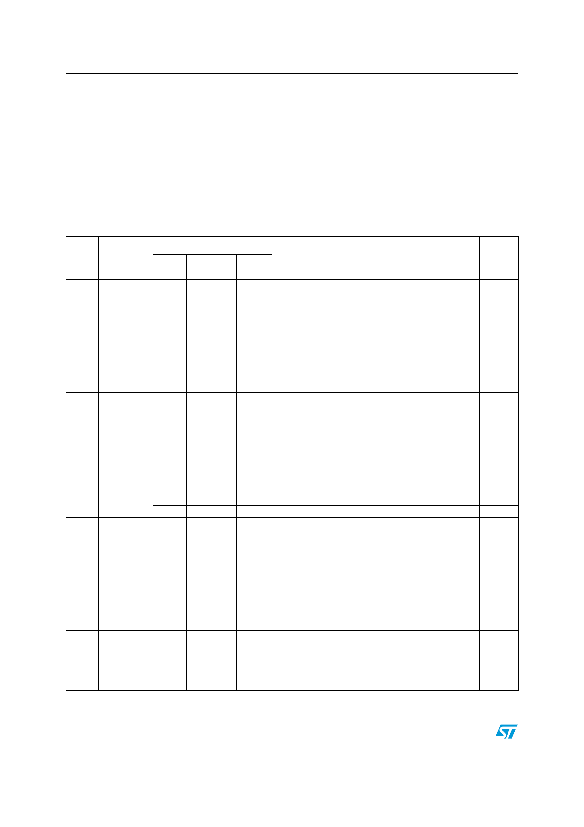
STM8 instruction set PM0044
7.2.5 Operation code notation
ee extended order byte of 24-bit extended address
ww high order byte of 16-bit long address or middle order byte of 24-bit extended address
bb short address or low order byte of 16-bit long address or 24-bit extended address
ii immediate data byte or low order byte of 16-bit immediate data
iw high order byte of 16-bit immediate data
rr relative offset byte in a range of [-128..+127]
7.3 Instruction set summary
Table 42. Instruction set summary
Effect on CC register
Description
Mnemo
ADC Add with carry
ADD
Add without
carry
VI1HI0N Z C
-
Set if the carry from R6 is
different from the carry bit C
-
Set if the carry from R6 is
different from the carry bit C
- - - - - - - ADD SP,#$12 SP ← SP + imm.b 5B ii 2
-
Set if R7 is set
cleared otherwise
Set if there is a carry from bit 3 to 4
-
Set if R7 is set
cleared otherwise
Set if there is a carry from bit 3 to 4
cleared otherwise
cleared otherwise
Set if R=$00
Set if R=$00
Syntax example Operation
ADC A,($12,SP)
cleared otherwise
cleared otherwise
Set if there is a carry from R7
ADD A,($12,SP) A ← A + M(SP+shortoff) 1B bb 1
cleared otherwise
cleared otherwise
Set if there is a carry from R7
A ← A + M(SP+shortoff) +
CC.C
Example
op-
code(s)
19 bb 1
(1)
Pipe
Cycles
ADDW
AND Logical AND
Add word
without carry
-
Set if the carry from R14 is
different from the carry bit C
---
-
-
Set if R=$0000
Set if R15 is set
Set if R7 is set
cleared otherwise
Set if R=$00
cleared otherwise
cleared otherwise
Set if there is a carry from bit 7 to 8
ADDW X,($12,SP) X ←-X + M(SP+shortoff) 72 FB bb 2
cleared otherwise
cleared otherwise
Set if there is a carry from R15
- AND A,($12,SP)
cleared otherwise
64/162 Doc ID 13590 Rev 3
A ← A AND
M(SP+shortoff)
14 bb 1
Page 65

PM0044 STM8 instruction set
Table 42. Instruction set summary (continued)
Effect on CC register
Description
Mnemo
BCCM
BCP
BCPL
BREAK
BRES Bit reset - - - - - - - BRES $1234,#1 M(longmem).bit ← 0
BSET Bit set - - - - - - - BSET $1234,#1 M(longmem).bit ← 1
BTJF
BTJT
CALL
CALLF
CALLR
CCF
CLR
CLRW
Copy carry
in memory bit
Logical bit
compare
Complement bit
in memory
Software
breakpoint
Bit test and
relative
jump if
condition is
false
Bit test and
relative
jump if
condition is true
Call to
Subroutine with
address in
same section
Call to
subroutine
with extended
address
Call Subroutine
relative
Complement
carry flag
Clears the
destination byte
Clears the
destination
index register
VI1HI0N Z C
- - - - - - - BCCM $1234,#1 M(longmem).bit ← CC.C
---
Set if R=$00
Set if R7 is set
cleared otherwise
- - - - - - - BCPL $1234,#1
----- - -SW-BREAK 8B 1Flush
----- -
----- -
- - - - - - - CALL [$1234.w]
- - - - - - - CALLF $123456
- - - - - - - CALLR label
----- -CCCF CC.C ← CC.C
- - - - 0 1 - CLR ([$1234.w],X)
- - - - 0 1 - CLRW X X ← 0x0000 5F 1
Syntax example Operation
test {A AND
- BCP A,($12,SP)
cleared otherwise
BTJF $1234,#1,label
bit
tested
BTJT $1234,#1,label
bit
tested
M(SP+shortoff) }
N and Z are updated
accordingly
M(longmem).bit ←
M(longmem).bit
if M(longmem).bit=0
if M(longmem).bit=1
PC← PC + 4
M(SP--) ← PCL
M(SP--) ← PCH
PCH← M(longmem)
PCL← M(longmem + 1)
PC ← PC+4
M(SP--) ← PCL
M(SP--) ← PCH
M(SP--) ← PCE
PC ← extmem
PC ← PC + 4
M(SP--) ← PCL
M(SP--) ← PCH
PC ← PC + rr
M( M(longmem).w + X ) ←
0x00
then PC ← PC + 4 + rr
else PC ← PC + 4
then PC ← PC + 4 + rr
else PC ← PC + 4
Example
op-
code(s)
90 1n ww bb
n= 2*bit
15 bb 1
90 1n ww bb
n= 2*bit
72 1n ww bb
n= 1 + 2*bit
72 1n ww bb
n= 2*bit
72 0n ww bb
n= 1 + 2*bit
72 0n ww bb
n= 2*bit
72 CD ww bb 6 Flush
8D ee ww bb 5 Flush
AD bb 4 Flush
8C 1
72 6F ww bb 4
2/3
2/3
(1)
Pipe
Cycles
1
1
1
1
Flush
(2)
Flush
(2)
CP Compare
---
overflows, cleared otherwise
Set if A-mem (signed values)
CP A,($12,SP) test { A - M(SP+shortoff) } 11 bb 1
Set if R=$00
Set if R7 is set
cleared otherwise
cleared otherwise
cleared otherwise
Set if A<mem (unsigned values)
Doc ID 13590 Rev 3 65/162
Page 66

STM8 instruction set PM0044
Table 42. Instruction set summary (continued)
Description
Mnemo
Effect on CC register
VI1HI0N Z C
Syntax example Operation
Example
op-
code(s)
(1)
Pipe
Cycles
CPW Compare word
CPL
CPLW
DEC
DECW
Logical 1’s
complement
Logical 1’s
complement
Decrement byte
by one
Decrement
word by one
---
overflows, cleared otherwise
Set if Xmmem (signed values)
---
cleared otherwise
Set if sign overflow
---
--
--
Set if R15 is set
Set if R7 is set
Set if R15 is set
Set if R7 is set
CPW X,($12,SP) test { X - M(SP+shortoff) } 13 bb 2
Set if R=$0000
cleared otherwise
cleared otherwise
cleared otherwise
Set if X<mem (unsigned values)
M(M(longmem).w +X) ←
1 CPL ([$1234.w],X)
Set if R=$00
cleared otherwise
cleared otherwise
1CPLW X
Set if R=$0000
cleared otherwise
cleared otherwise
- DEC ([$1234.w],X)
Set if R=$00
cleared otherwise
cleared otherwise
-DECW X X← X - 1 5A 1
FF - M(M(longmem).w+X)
or
M(M(longmem).w+X)
XOR FF
X ← FFFF - X
or
X XOR FFFF
M(M(longmem).w + X) ←
M(M(longmem).w + X) - 1
72 63 ww bb 4
53 2
72 6A ww bb 4
Set if R=$0000
Set if R15 is set
cleared otherwise
cleared otherwise
Set if Q=$0000
cleared otherwise
Set if Q=$0000
cleared otherwise
DIV X,A
DIV Y,A
Set if divide by 0
cleared otherwise
DIVW X,Y
Set if divide by 0
cleared otherwise
EXG A,$1234 A ↔ M(longmem) 31 ww bb 3
EXG A,XL A ↔ XL 41 1
EXG A,YL A ↔ YL 61 1
DIV
DIVW
EXG
EXGW
HALT
16 by 8
Unsigned
division
16 by 16
Unsigned
division
Data byte
exchange
Data word
exchange
Halt oscillator
(CPU +
Peripherals)
cleared otherwise
Set if sign overflow
0-0-0
0-0-0
----- - -
----- - -EXGW X,Y X ↔ Y511
-1-0- - -HALT
66/162 Doc ID 13590 Rev 3
X ← X/A (Quotient)
A ← X%A (Remainder)
Y ← Y/A (Quotient)
A ← Y%A (Remainder)
X ← X/Y (Quotient)
Y ← X%Y (Remainder)
CC.I0 ← 0 , CC.I1 ← 1
Oscillator stopped till an
interrupt occurs
62 16
90 62 16
65 16
8E 10
Page 67

PM0044 STM8 instruction set
Table 42. Instruction set summary (continued)
Description
Mnemo
Effect on CC register
VI1HI0N Z C
Syntax example Operation
Example
op-
code(s)
(1)
Pipe
Cycles
Increment byte
INC
INCW
INT Interrupt - - - - - - - INT $123456 PC ← extmem 82 ee ww bb 2
IRET Interrupt return
JP
JPF
JRA
JRC Jump if C = 1 - - - - - - - JRC Label
JREQ
JRF Never Jump - - - - - - - JRF Label ---------------- 21 bb 1
JRH Jump if H = 1 - - - - - - - JRH Label
JRIH
JRIL
JRM
JRMI
JRNC jump if C = 0 - - - - - - - JRNC Label
by one
Increment word
by one
Jump to an
address in
section 0
Jump to
an extended
address
Unconditional
relative jump
Jump if Z =
1(equal)
Jump if Por t INT
pin = 1
Jump if Por t INT
pin = 0
Jump if
Interrupts are
masked
Jump if N =
1(minus)
---
cleared otherwise
Set if sign overflow
---
cleared otherwise
Set if sign overflow
Updated according to the value pop
from the stack into CC register
- - - - - - - JP ([$1234.w],X) PC ← M(longmem).w + X 72 DC ww bb 5 Flush
- - - - - - - JPF $123456 PC ← extmem AC ee ww bb 2 Flush
- - - - - - - JRA Label PC ← PC + 2+ rr 20 bb 2 Flush
- - - - - - - JREQ Label
- - - - - - - JRIH Label
- - - - - - - JRIL Label
- - - - - - - JRM Label
- - - - - - - JRMI Label
Set if R7 is set
Set if R15 is set
- INC ([$1234.w],X)
Set if R=$00
cleared otherwise
cleared otherwise
- INCW X X ← X + 1 5C 2
Set if R=$0000
cleared otherwise
cleared otherwise
IRET
M(M(longmem).w + X) ←
M(M(longmem).w + X) + 1
(++SP)
CC ← M(++SP)
A ← M(++SP)
X ← M(++SP); SP++
Y ← M(++SP); SP++
PCE ← M(++SP)
PCH ← M(++SP)
PCL ← M(++SP)
if CC.C =1
then PC ← PC + 2+ rr
else PC ← PC + 2
if CC.Z = 1
then PC ← PC + 2+ rr
else PC ← PC + 2
if CC.H = 1
then PC ← PC + 2+ rr
else PC ← PC + 2
if Port INT pin =1
then PC ← PC + 2+ rr
else PC ← PC + 2
if Port INT pin = 0
then PC ← PC + 2+ rr
else PC ← PC + 2
if I0 AND I1 = 1
then PC ← PC + 2 + rr
else PC ← PC + 2
if CC.N = 1
then PC ← PC + 2+ rr
else PC ← PC + 2
if CC.C =0
then PC ← PC + 2+ rr
else PC ← PC + 2
72 6C ww bb 4
80 11 Flush
25 bb 1/2
27 bb 1/2
90 29 bb 1/2
90 2F bb 1/2
90 2E bb 1/2
90 2D bb 1/2
2B bb 1/2
24 bb 1/2
Flush
(2)
Flush
(2)
Flush
(2)
Flush
(2)
Flush
(2)
Flush
(2)
Flush
(2)
Flush
(2)
Doc ID 13590 Rev 3 67/162
Page 68

STM8 instruction set PM0044
Table 42. Instruction set summary (continued)
Effect on CC register
Description
Mnemo
JRNE
JRNH Jump if H = 0 - - - - - - - JRNH Label
JRNM
JRNV jump if V = 0 - - - - - - - JRNV Label
JRPL
JRSGE
JRSGT
JRSLE
JRSLT
JRT Jump relative - - - - - - - JRT Label PC ← PC + 2+ rr 20 bb 2 Flush
JRUGE Jump if C = 0 - - - - - - - JRUGE Label
JRUGT
JRULE
JRULT Jump if C = 1 - - - - - - - JRULT Label
JRV Jump if V = 1 - - - - - - - JRV Label
Jump if Z =0
(not equal)
Jump if
Interrupts are
not masked
Jump if
N = 0 (plus)
Jump if
(N xor V) = 0
Jump if
(Z or (N xor V))
= 0
Jump if
(Z or (N xor V))
= 1
Jump if
(N xor V) = 1
Jump if
(C+Z = 0)
Jump if
(C+Z =1)
A register load
VI1HI0N Z C
- - - - - - - JRNE Label
- - - - - - - JRNM Label
- - - - - - - JRPL Label
- - - - - - - JRSGE Label
- - - - - - - JRSGT Label
- - - - - - - JRSLE Label
- - - - - - - JRSLT Label
- - - - - - - JRUGT Label
- - - - - - - JRULE Label
Syntax example Operation
if CC.Z = 0
then PC ← PC + 2+ rr
else PC ← PC + 2
if CC.H = 0
then PC ← PC + 2+ rr
else PC ← PC + 2
if I0 AND I1= 0
then PC ← PC + 2 + rr
else PC ← PC + 2
if CC.C =0
then PC ← PC + 2+ rr
else PC ← PC + 2
if CC.N = 0
then PC ← PC + 2+ rr
else PC ← PC + 2
if (CC.N xor CC.V) = 0
then PC ← PC + 2+ rr
else PC ← PC + 2
if (CC.Z or (CC.N xor
CC.V)) = 0
then PC ← PC + 2+ rr
else PC ← PC + 2
if (CC.Z or (CC.N xor
CC.V)) = 1
then PC ← PC + 2+ rr
else PC ← PC + 2
if (CC.N xor CC.V) = 1
then PC ← PC + 2+ rr
else PC ← PC + 21
if CC.C = 0
then PC ← PC + 2+ rr
else PC ← PC + 2
if (CC.C = 0 and CC.Z = 0)
then PC ← PC + 2+ rr
else PC ← PC + 2
if (CC.C = 1 and CC.Z = 1)
then PC ← PC + 2+ rr
else PC ← PC + 2
if CC.C = 1
then PC ← PC + 2+ rr
else PC ← PC + 21
if CC.V =1
then PC ← PC + 2+ rr
else PC ← PC + 2
LD A,($12,SP) A ← M(SP+shortoff) 7B bb 1
Example
op-
code(s)
26 bb 1/2
90 28 bb 1/2
90 2C bb 1/2
28 bb 1/2
2A bb 1/2
2E bb 1/2
2C bb 1/2
2D bb 1/2
2F bb 1/2
24 bb 1/2
22 bb 1/2 Flush
23 bb 1/2 Flush
25 bb 1/2
29 bb 1/2 Flush
(1)
Cycles
Flush
(2)
Flush
(2)
Flush
(2)
Flush
(2)
Flush
(2)
Flush
(2)
Flush
(2)
Flush
(2)
Flush
(2)
Flush
(2)
Flush
(2)
Pipe
A register store LD ($12,SP),A M(SP+shortoff) ← A6B bb 1
LD
Register to
register move
----
Set if R7 is set
- - LD A, XH A ← XH 95 1
Set if R=$00
cleared otherwise
cleared otherwise
-
68/162 Doc ID 13590 Rev 3
Page 69

PM0044 STM8 instruction set
Table 42. Instruction set summary (continued)
Effect on CC register
Description
Mnemo
Data load /
LDF
store
with extended
address
X register load
X register store LDW ($12,SP),X M(SP+shortoff) ← X1F bb 2
Y register load LDW Y,($12,SP) Y ← M(SP+shortoff) 16 bb 2
VI1HI0N Z C
----
Set if R=$00
Set if R7 is set
cleared otherwise
Syntax example Operation
LDF A,($123456,X) A ← M(X+extoff)
LDF A,($123456,Y) A ← M(Y+extoff)
LDF A,([$1234.e],X) A ← M(X+[longptr.e]) 92 AF ww bb 5
LDF ($123456,X),A M(X+extoff) ← A
cleared otherwise
LDF ($123456,Y),A M(Y+extoff) ← A
LDF ([1234.e],X),A M(X+[longptr.e]) ← A 92 A7 ww bb 5
LDW X,($12,SP) X ← M(SP+shortoff) 1E bb 2
Example
op-
code(s)
AF ee ww
bb
90 AF ee ww
bb
A7 ee ww
bb
90 A7 ee ww
bb
(1)
Pipe
Cycles
1
1
1
1
Y register store LDW ($12,SP),Y M(SP+shortoff) ← Y 17 bb 2
LDW
SP register load
/ store
Index register
move
MOV Data byte move - - - - - - -
8 by 8
MUL
NEG
NEGW
NOP No operation - - - - - - - NOP --------- 9D 1
multiplication
(unsigned)
Logical 2’s
complement
Logical 2’s
complement
----
--0---0
---
Set if M=$80
cleared otherwise
---
Set if X=$8000
cleared otherwise
Set if R=$0000
Set if R15 is set
cleared otherwise
cleared otherwise
--
Set if R=$00
Set if R7 is set
cleared otherwise
cleared otherwise
Set if R=$0000
Set if R15 is set
cleared otherwise
cleared otherwise
-
LDW SP,X SP ← X941
LDW X,SP X ← SP 96 1
LDW X, Y X ← Y931
MOV $1234,#$12 M(longmem) ← imm.b 35 ii ww bb 1
MOV $12,$34
MOV mem1,mem2
MOV $1234,$5678
MOV mem1,mem2
MUL X,A X ← X*A 42 4
MUL Y,A Y ← Y*A 90 42 4
NEG ([$1234.w],X)
set otherwise
Cleared if R=$00
NEGW X X ← 0000 - X 50 2
set otherwise
Cleared if R=$0000
M(mem1.b) ←
M(mem2.b)
M(mem1.w) ←
M(mem2.w)
M(M(longmem) + X) ←
00 - M(M(longmem) + X)
44 b2 b1 1
45 w2 b2 w1
b1
72 60 ww bb 4
1
OR Logical OR - - - -
POP
Pop data byte
from stack
Pop
code condition
register
- - - - - - - POP $1234 M(longmem) ← M(++SP) 32 ww bb 1
- OR A,($12,SP) A ← A OR M(SP+shortoff) 1A bb 1
Set if R=$00
Set if R7 is set
cleared otherwise
cleared otherwise
POP CC CC ← M(++SP) 86 1
Doc ID 13590 Rev 3 69/162
Page 70

STM8 instruction set PM0044
Table 42. Instruction set summary (continued)
Effect on CC register
Description
Mnemo
POPW
PUSH
PUSHW
RCF Reset carry flag - - - - - - 0 RCF CC.C ← 0981
RET
RETF
RIM
RLC
Pop index
register from
stack
Push
data byte onto
stack
Push index
register onto
stack
Subroutine
return
from section 0
Subroutine
return
from extended
address
Reset interrupt
mask/
Interrupt enable
Rotate left
logical through
carry
VI1HI0N Z C
----- - -POPW X
----- - -
----- - -PUSHW X
----- - -RET
----- - -RETF
-1-0- - -RIM CC.I1 ← 19A1
----
Set if R=$00
Set if R7 is set
cleared otherwise
Syntax example Operation
XH ← M(++SP)
XL ← M(++SP)
PUSH $1234 M(SP--) ← M(longmem) 3B ww bb 1
PUSH #$12 M(SP--) ← imm.b 4B bb 1
M(SP--) ← XL
M(SP--) ← XH
PCH ← M(++SP)
PCL ← M(++SP)
PCE ← M(++SP)
PCH ← M(++SP)
PCL ← M(++SP)
R0 ← CC.C
R1 ← bit 0
R2 ← bit 1
RLC ([$1234.w],X)
cleared otherwise
Bit 7 of the byte before rotation
R3 ← bit 2
R4 ← bit 3
R5 ← bit 4
R6 ← bit 5
R7 ← bit 6
CC.C ← bit 7
Example
op-
code(s)
85 2
89 2
81 4 Flush
87 5 Flush
72 69 ww bb 4
(1)
Pipe
Cycles
RLWA
RRC
Rotate word left
logical through
carry
Rotate word left
through
Accumulator
Rotate right
logical through
carry
----
----
----
Set if R15 is set
Set if R15 is set
Set if R7 is set
Set if R=$0000
cleared otherwise
Set if R=$0000
cleared otherwise
Set if R=$00
cleared otherwise
RLCW X
cleared otherwise
Bit 7 of the byte before rotation
-RLWA X
cleared otherwise
RRC ([$1234.w],X)
cleared otherwise
Bit 0 of the byte before rotation
RLCW
70/162 Doc ID 13590 Rev 3
R0 ← CC.C
R1 ← bit 0
R2 ← bit 1
...
R13 ← bit 12
R14 ← bit 13
R15 ← bit 14
CC.C ← bit 15
A ← XH
XH ← XL
XL ← A
R7 ← CC.C
R6 ← bit 7
R5 ← bit 6
R4 ← bit 5
R3 ← bit 4
R2 ← bit 3
R1 ← bit 2
R0 ← bit 1
CC.C ← bit 0
59 2
02 1
72 66 ww bb 4
Page 71

PM0044 STM8 instruction set
Table 42. Instruction set summary (continued)
Mnemo
RRCW
Description
Rotate word
right logical
through carry
Effect on CC register
VI1HI0N Z C
----
Set if R=$00
Set if R7 is set
cleared otherwise
cleared otherwise
Bit 0 of the byte before rotation
Syntax example Operation
R15 ← CC.C
R14 ← bit 15
R13 ← bit 14
RRCW X
...
R2 ← bit 3
R1 ← bit 2
R0 ← bit 1
CC.C ← bit 0
Example
op-
code(s)
56 2
(1)
Pipe
Cycles
RRWA
RVF
SBC
SCF Set Carry Flag - - - - - - 1 SCF CC.C ← 1991
SIM
SLA
Rotate word
right through
Accumulator
Reset overflow
flag
Subtract with
carry
Set interrupt
mask/
Disable
interrupts
Shift left
arithmetic
----
Set if R15 is set
0---- - -RVF CC.V ← 09C1
---
Set if R7 is set
an overflow, cleared otherwise
Set if the signed subtraction generates
-1-1- - -SIM
----
Set if R7 is set
Set if R=$0000
cleared otherwise
cleared otherwise
Set if R=$00
cleared otherwise
cleared otherwise
Set if R=$00
cleared otherwise
cleared otherwise
-RRWA X
SBC A,($12,SP)
cleared otherwise
Set if there is a carry from R7
SLA ([$1234.w],X)
Bit 7 of the byte before shifting
A ← XL
XL ← XH
XH ← A
A ← A -M(SP+shortoff) CC.C
CC.I0 ← 1
CC.I1 ← 1
R0 ← 0
R1 ← bit 0
R2 ← bit 1
R3 ← bit 2
R4 ← bit 3
R5 ← bit 4
R6 ← bit 5
R7 ← bit 6
CC.C ← bit 7
01 1
12 bb 1
9B 1
72 68 ww bb 4
Doc ID 13590 Rev 3 71/162
Page 72

STM8 instruction set PM0044
Table 42. Instruction set summary (continued)
Effect on CC register
Description
Mnemo
SLAW
SLL Shift left logical - - - -
Shift word left
arithmetic
VI1HI0N Z C
----
Set if R15 is set
Set if R7 is set
Set if R=$0000
cleared otherwise
Set if R=$00
cleared otherwise
Syntax example Operation
R0 ← 0
R1 ← bit 0
R2 ← bit 1
SLAW X
cleared otherwise
Bit 15 of the byte before shifting
SLL ([$1234.w],X)
cleared otherwise
Bit 7 of the byte before shifting
R3 ← bit 2
.....
R14 ← bit 13
R15 ← bit 14
CC.C ← bit 15
R0 ← 0
R1 ← bit 0
R2 ← bit 1
R3 ← bit 2
R4 ← bit 3
R5 ← bit 4
R6 ← bit 5
R7 ← bit 6
CC.C ← bit 7
Example
op-
code(s)
58 2
72 68 ww bb 4
(1)
Pipe
Cycles
SLLW
SRA
SRAW
Shift word left
logical
Shift right
arithmetic
Shift word right
arithmetic
----
----
---
Set if R7 set
cleared otherwise
Set if R15 is set
Set if R7 is set
Set if R15 is set
cleared otherwise
cleared otherwise
cleared otherwise
Set if R=$0000
Set if R=$00
Set if R=$0000
SLLW X
cleared otherwise
Bit 15 of the byte before shifting
SRA ([$1234.w],X)
cleared otherwise
Bit 0 of the byte before shifting
SRAW X
cleared otherwise
Bit 0 of the byte before shifting
R0 ← 0
R1 ← bit 0
R2 ← bit 1
R3 ← bit 2
.....
R14 ← bit 13
R15 ← bit 14
CC.C ← bit 15
CC.C ← bit 0
R0 ← bit 1
R1 ← bit 2
R2 ← bit 3
R3 ← bit 4
R4 ← bit 5
R5 ← bit 6
R6 ← bit 7
R7 ← bit 7 (unchanged)
CC.C ← bit 0
R0 ← bit 1
R1 ← bit 2
R2 ← bit 3
....
R12 ← bit 13
R13 ← bit 14
R14 ← bit 15
R15 ← bit 15 (unchanged)
58 2
72 67 ww bb 4
57 2
72/162 Doc ID 13590 Rev 3
Page 73
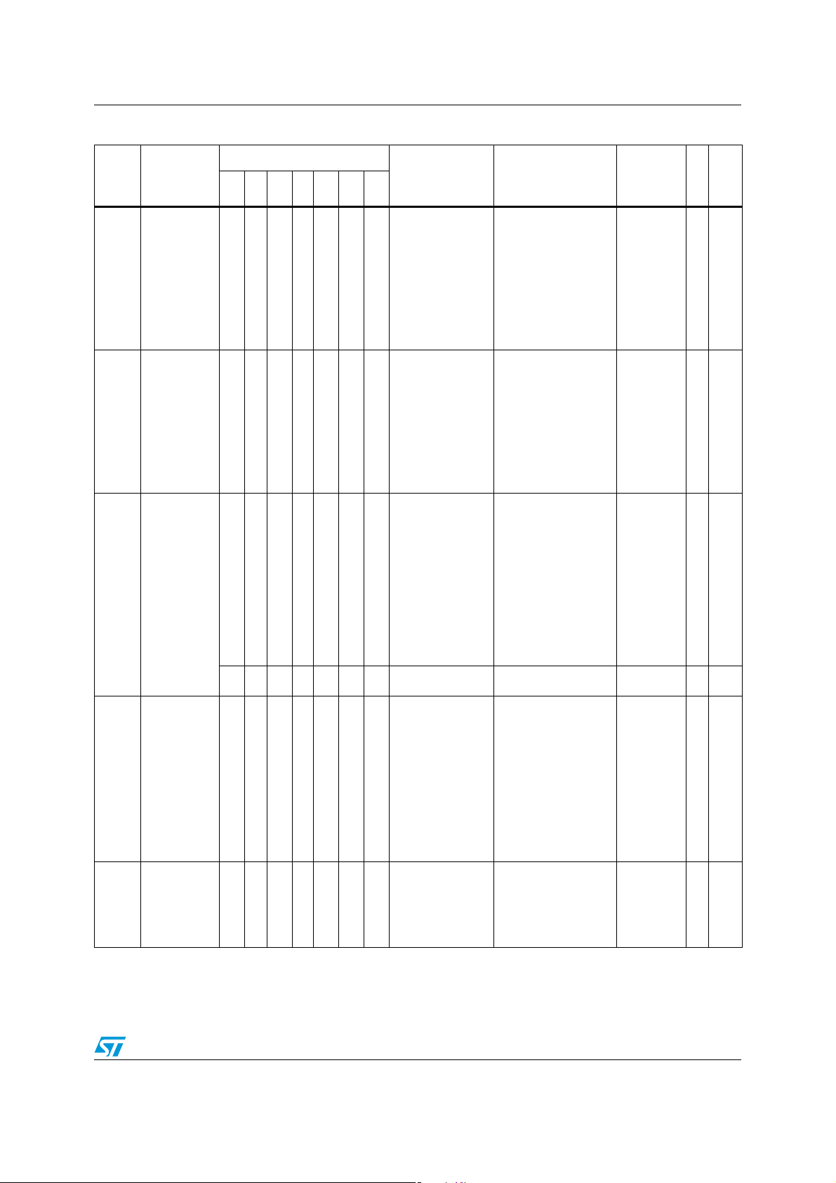
PM0044 STM8 instruction set
Table 42. Instruction set summary (continued)
Mnemo
SRL
SRLW
Description
Shift right
logical
Shift word right
arithmetic
Effect on CC register
VI1HI0N Z C
----
Set if R7 set
Set if R=$00
cleared otherwise
cleared otherwise
Bit 0 of the byte before shifting
----
Set if R15 set
Set if R=$0000
cleared otherwise
cleared otherwise
Bit 0 of the byte before shifting
Syntax example Operation
CC.C ← bit 0
R0 ← bit 1
R1 ← bit 2
SRL ([$1234.w],X)
SRLW X
R2 ← bit 3
R3 ← bit 4
R4 ← bit 5
R5 ← bit 6
R6 ← bit 7
R7 ← 0
CC.C ← bit 0
R0 ← bit 1
R1 ← bit 2
R2 ← bit 3
....
R12 ← bit 13
R13 ← bit 14
R14 ← bit 15
R15 ← 0
Example
op-
code(s)
72 64 ww bb 4
54 2
(1)
Pipe
Cycles
Subtract without
SUB
SUBW
SWAP Swap nibbles - - - -
carry
Subtract word
without carry
---
an overflow, cleared otherwise
Set if the signed operation generates
- - - - - - - SUB SP,#$12 SP ← SP + imm.b 52 ii 2
-
Set if dst(7:0)< mem(7:0)
values), cleared otherwise
Set if X< mem (unsigned 16-bit
(unsigned values) cleared otherwise
SUB A,($12,SP) A ← A -M(SP+shortoff) 10 bb 1
Set if R=$00
Set if R7 is set
cleared otherwise
cleared otherwise
cleared otherwise
Set if there is a carry from R7
-
Set if R=$0000
Set if R15 is set
cleared otherwise
Set if R=$00
Set if R7 is set
cleared otherwise
SUBW X,($12,SP) X ← X -M(SP+shortoff) 72 F0 bb 2
cleared otherwise
cleared otherwise
Set if dst < mem (unsigned values)
R0 ↔ R4
- SWAP ([$1234.w],X)
cleared otherwise
R1 ↔ R5
R2 ↔ R6
R3 ↔ R7
72 6E ww bb 4
Doc ID 13590 Rev 3 73/162
Page 74

STM8 instruction set PM0044
Table 42. Instruction set summary (continued)
Effect on CC register
Description
Mnemo
SWAPW Swap bytes - - - -
VI1HI0N Z C
Set if R15 is set
Set if R=$0000
cleared otherwise
Syntax example Operation
R0 ↔ R8
R1 ↔ R9
R2 ↔ R10
- SWAPW X
cleared otherwise
R3 ↔ R11
R4 ↔ R12
R5 ↔ R13
R6 ↔ R14
R7 ↔ R15
Example
op-
code(s)
5E 1
(1)
Pipe
Cycles
TNZ
TNZW
TRAP
WFE
WFI
Test fo r
negative or zero
Test wo r d fo r
negative or zero
Software
interrupt
Wait for eve nt
(CPU stopped,
Low power
mode)
Wait for
interrupt
(CPU stopped,
Low power
mode)
----
Set if R7 is set
----
Set if R15 is set
-1-1- - -TRAP
----- - -WFE
-1-0- - -WFI
- TNZ ([$1234.w],X)
Set if R=$00
cleared otherwise
cleared otherwise
-TNZW X
Set if R=$0000
cleared otherwise
cleared otherwise
CC.N ← R7
CC.Z ← 1 if R=$00
← 0 otherwise
CC.N ← R15
CC.Z ← 1 if R=$0000
← 0 otherwise
PC ← PC+1
M(SP--) ← PCL
M(SP--) ← PCH
M(SP--) ← PCE
M(SP--) ← YL
M(SP--) ← YH
M(SP--) ← XL
M(SP--) ← XH
M(SP--) ← A
M(SP--) ← CC
PC ← TRAP vector
address
CPU clock stopped till the
event input is activated.
Internal peripherals are
still running
CC.I0 ← 0, CC.I1 ← 1
CPU clock stopped till an
interrupt occurs. Internal
peripherals are still
running
72 6D ww bb 4
5D 2
83 9 Flush
72 8F 1
8F 10
XOR
Logical
exclusive OR
----
Set if R7 is set
- XOR A,($12,SP)
Set if R=$00
cleared otherwise
cleared otherwise
1. Number of cycles corresponding to the example op-code.
2. If branch taken.
7.4 Instruction set
The following pages give a detailed description of each STM8 instruction.
74/162 Doc ID 13590 Rev 3
A ← A XOR
M(SP+shortoff)
18 bb 1
Page 75

PM0044 STM8 instruction set
ADC
Addition with Carry
ADC
Syntax ADC A, src e.g. ADC A,#$15
Operation A <= A+ src + C
Description The source byte, along with the carry flag, is added to the contents of the
accumulator and the result is stored in the accumulator. This instruction is
useful for addition of operands that are larger than eight.
The source is
a memory or data byte.
Instruction overview:
mnem dst src
ADC A Mem V-H-NZC
V ⇒ (A7.M7 + M7.R7
+ R7.A7) ⊕ (A6.M6 + M6.R6 + R6.A6)
VI1HI0NZC
Affected condition flags
Set if the signed operation generates an overflow, cleared otherwise.
H ⇒ A3.M3 + M3.R3
+ R3.A3
Set if a carry occurred from bit 3 of the result, cleared otherwise.
N ⇒ R7
Set if bit 7 of the result is set (negative value), cleared otherwise.
Z ⇒ R7
.R6.R5.R4.R3.R2.R1.R0
Set if the result is zero (0x00), cleared otherwise.
C ⇒ A7.M7 + M7.R7
+ R7.A7
Set if a carry occurred from bit 7 of the result, cleared otherwise.
Doc ID 13590 Rev 3 75/162
Page 76
STM8 instruction set PM0044
Detailed description:
dst src Asm cy lgth Op-code(s) ST7
A #byte ADC A,#$55 1 2 A9 XX ✗
A shortmem ADC A,$10 1 2 B9 XX ✗
A longmem ADC A,$1000 1 3 C9 MS LS ✗
A (X) ADC A,(X) 1 1 F9 ✗
A (shortoff,X) ADC A,($10,X) 1 2 E9 XX ✗
A (longoff,X) ADC A,($1000,X) 1 3 D9 MS LS ✗
A (Y) ADC A,(Y) 1 2 90 F9 ✗
A (shortoff,Y) ADC A,($10,Y) 1 3 90 E9 XX ✗
A (longoff,Y) ADC A,($1000,Y) 1 4 90 D9 MS LS ✗
A (shortoff,SP) ADC A,($10,SP) 1 2 19 XX
A [shortptr.w] ADC A,[$10.w] 4 3 92 C9 XX ✗
A [longptr.w] ADC A,[$1000.w] 4 4 72 C9 MS LS
A ([shortptr.w],X) ADC A,([$10.w],X) 4 3 92 D9 XX ✗
A ([longptr.w],X) ADC A,([$1000.w],X) 4 4 72 D9 MS LS
A ([shortptr.w],Y) ADC A,([$10.w],Y) 4 3 91 D9 XX ✗
See also: ADD, SUB, SBC, MUL, DIV
76/162 Doc ID 13590 Rev 3
Page 77

PM0044 STM8 instruction set
ADD
Addition
ADD
Syntax ADD A,src e.g. ADD A,#%11001010
Operation A <= A+ src
Description The source byte is added to the contents of the accumulator and the result
is stored in the accumulator. The source is a memory or data byte.
Instruction overview
mnem dst src
ADD A Mem V-H-NZC
V ⇒ (A7.M7 + M7.R7
+ R7.A7) ⊕ (A6.M6 + M6.R6 + R6.A6)
VI1HI0N ZC
Affected condition flags
Set if the signed operation generates an overflow, cleared otherwise.
H ⇒ A3.M3 + M3.R3
+ R3.A3
Set if a carry occurred from bit 3 of the result, cleared otherwise.
N ⇒ R7
Set if bit 7 of the result is set (negative value), cleared otherwise.
Z ⇒ R7
.R6.R5.R4.R3.R2.R1.R0
Set if the result is zero (0x00), cleared otherwise.
C ⇒ A7.M7 + M7.R7
+ R7.A7
Set if a carry occurred from bit 7 of the result, cleared otherwise.
Detailed description
dst src Asm cy lgth Op-code(s) ST7
A #byte ADD A,#$55 1 2 AB XX ✗
A shortmem ADD A,$10 1 2 BB XX ✗
A longmem ADD A,$1000 1 3 CB MS LS ✗
A (X) ADD A,(X) 1 1 FB ✗
A (shortoff,X) ADD A,($10,X) 1 2 EB XX ✗
A (longoff,X) ADD A,($1000,X) 1 3 DB MS LS ✗
A (Y) ADD A,(Y) 1 2 90 FB ✗
A (shortoff,Y) ADD A,($10,Y) 1 3 90 EB XX ✗
A (longoff,Y) ADD A,($1000,Y) 1 4 90 DB MS LS ✗
A (shortoff,SP) ADD A,($10,SP) 1 2 1B XX
A [shortptr.w] ADD A,[$10.w] 4 3 92 CB XX ✗
A [longptr.w] ADD A,[$1000.w] 4 4 72 CB MS LS
A ([shortptr.w],X) ADD A,([$10.w],X) 4 3 92 DB XX ✗
A ([longptr.w],X) ADD A,([$1000.w],X) 4 4 72 DB MS LS
A ([shortptr.w],Y) ADD A,([$10.w],Y) 4 3 91 DB XX ✗
See also: ADDW, ADC, SUB, SBC, MUL, DIV
Doc ID 13590 Rev 3 77/162
Page 78
STM8 instruction set PM0044
ADDW
Word Addition with index registers
ADDW
Syntax ADDW dst,src e.g. ADDW X,#$1000
Operation dst <= dst + src
Description The source (16-bit) is added to the contents of the destination, which is an
index register (X/Y) and the result is stored in the same index register. The
source is a 16-bit memory or data word. The ADDW instruction can also be
used to add an immediate value to the stack pointer (SP).
Instruction overview
mnem dst src
ADDW X Mem V - H - N Z C
ADDW Y Mem V - H - N Z C
ADDW SP Imm -------
V ⇒ (A15.M15 + M15.R15
+ R15.A15) ⊕ (A14.M14 + M14.R14 + R14.A14)
VI1HI0NZC
Affected condition flags
Set if the signed operation generates an overflow, cleared otherwise.
H ⇒ X7.M7 + M7.R7
+ R7.X7
Set if a carry occurred from bit 7 of the result, cleared otherwise.
N ⇒ R15
Set if bit 15 of the result is set (negative value), cleared otherwise.
Z ⇒ R15
.R14.R13.R12.R11.R10.R9.R8.R7.R6.R5.R4.R3.R2.R1.R0
Set if the result is zero (0x0000), cleared otherwise.
C ⇒ X15.M15 + M15.R15
+ R15.X15
Set if a carry occurred from bit 15 of the result, cleared otherwise.
Detailed description
dst src Asm cy lgth Op-code(s) ST7
X #word ADDW X,#$1000 2 3 1C MS LS
X longmem ADDW X,$1000 2 4 72 BB MS LS
X (shortoff,SP) ADDW X,($10,SP) 2 3 72 FB XX
Y #word ADDW Y,#$1000 2 4 72 A9 MS LS
Y longmem ADDW Y,$1000 2 4 72 B9 MS LS
Y (shortoff,SP) ADDW Y,($10,SP) 2 3 72 F9 XX
SP #byte ADDW SP,#$9 2 2 5B XX
See also: ADD, ADC, SUB, SBC, MUL, DIV
78/162 Doc ID 13590 Rev 3
Page 79

PM0044 STM8 instruction set
AND
Logical AND
AND
Syntax AND A,src e.g. AND A,#%00110101
Operation A <= A AND src
Description The source byte, is ANDed with the contents of the accumulator and the
result is stored in the accumulator. The source is a memory or data byte.
Truth table:
AND 0 1
000
101
Instruction overview
mnem dst src
VI1HI0NZ C
AND A Mem - - - - N Z -
Affected condition flags
N ⇒ R7
Set if bit 7 of the result is set (negative value), cleared otherwise.
Z ⇒ R7
.R6.R5.R4.R3.R2.R1.R0
Set if the result is zero (0x00), cleared otherwise.
Detailed description
dst src Asm cy lgth Op-code(s) ST7
A #byte AND A,#$55 1 2 A4 XX ✗
A shortmem AND A,$10 1 2 B4 XX ✗
A longmem AND A,$1000 1 3 C4 MS LS ✗
A (X) AND A,(X) 1 1 F4 ✗
A (shortoff,X) AND A,($10,X) 1 2 E4 XX ✗
A (longoff,X) AND A,($1000,X) 1 3 D4 MS LS ✗
A (Y) AND A,(Y) 1 2 90 F4 ✗
A (shortoff,Y) AND A,($10,Y) 1 3 90 E4 XX ✗
A (longoff,Y) AND A,($1000,Y) 1 4 90 D4 MS LS ✗
A (shortoff,SP) AND A,($10,SP) 1 2 14 XX
A [shortptr.w] AND A,[$10.w] 4 3 92 C4 XX ✗
A [longptr.w] AND A,[$1000.w] 4 4 72 C4 MS LS
A ([shortptr.w],X) AND A,([$10.w],X) 4 3 92 D4 XX ✗
A ([longptr.w],X)
A ([shortptr.w],Y) AND A,([$1000],Y) 4 3 91 D4 XX ✗
AND
A,([$1000.w],X)
4472D4MSLS
See also: OR, XOR, CPL, NEG
Doc ID 13590 Rev 3 79/162
Page 80

STM8 instruction set PM0044
BCCM
Copy Carry Bit to Memory
BCCM
Syntax BCCM dst, #pos (pos=0..7) e.g. BCCM $1234,#1
Operation dst(pos) <= CC.C
Description Copies the Carry flag of the Condition Code (CC) register in the bit
position of the memory location given by the destination address.
M(longmem).bit <- CC.C
Instruction overview
mnem dst bit position
VI1HI0NZC
BCCM Mem #pos -------
Affected condition flags
Detailed description
dst pos = 0..7 Asm cy lgth Op-code(s) ST7
longmem n =1+2*pos BCCM $1000,#2 1 4 90 1n MS LS
See also: LD, RCF, SCF
80/162 Doc ID 13590 Rev 3
Page 81

PM0044 STM8 instruction set
BCP
Logical Bit Compare
BCP
Syntax BCP A,src
Operation {N, Z} <= A AND src
Description The source byte, is ANDed to the contents of the accumulator. The result is
lost but condition flags N and Z are updated accordingly. The source is a
memory or data byte. This instruction can be used to perform bit tests on
A.
Instruction overview
mnem dst src
VI1HI0NZC
BCP A Mem ----NZ-
Affected condition flags
N ⇒ R7
Set if bit 7 of the result is set (negative value), cleared otherwise.
Z ⇒ R7
.R6.R5.R4.R3.R2.R1.R0
Set if the result is zero (0x00), cleared otherwise.
Detailed description
dst src Asm cy lgth Op-code(s) ST7
A #byte BCP A,#$55 1 2 A5 XX ✗
A shortmem BCP A,$10 1 2 B5 XX ✗
A longmem BCP A,$1000 1 3 C5 MS LS ✗
A (X) BCP A,(X) 1 1 F5 ✗
A (shortoff,X) BCP A,($10,X) 1 2 E5 XX ✗
A (longoff,X) BCP A,($1000,X) 1 3 D5 MS LS ✗
A (Y) BCP A,(Y) 1 2 90 F5 ✗
A (shortoff,Y) BCP A,($10,Y) 1 3 90 E5 XX ✗
A (longoff,Y) BCP A,($1000,Y) 1 4 90 D5 MS LS ✗
A (shortoff,SP) BCP A,($10,SP) 1 2 15 XX
A [shortptr.w] BCP A,[$10.w] 4 3 92 C5 XX ✗
A [longptr.w] BCP A,[$1000.w] 4 4 72 C5 MS LS
A ([shortptr.w],X) BCP A,([$10.w],X) 4 3 92 D5 XX ✗
A ([longptr.w],X) BCP A,([$1000.w],X) 4 4 72 D5 MS LS
A ([shortptr.w],Y) BCP A,([$10.w],Y) 4 3 91 D5 XX ✗
See also: CP, TNZ
Doc ID 13590 Rev 3 81/162
Page 82

STM8 instruction set PM0044
BCPL
Bit Complement
BCPL
Syntax BCPL dst, #pos (pos=0..7) e.g. BCPL PADR,#4
Operation dst(pos) <= 1 - dst(pos)
Description Complements the bit position in destination location. Leaves all other bits
unchanged.
M(longmem).bit <- -M(longmem).bit
Instruction overview
mnem dst
VI1HI0NZ C
BCPL Mem -------
Affected condition flags
Detailed description
dst pos = 0..7 Asm cy lgth Op-code(s) ST7
longmem n = 2*pos BCPL $1000,#2 1 4 90 1n MS LS
See also: CPL, BRES, BSET
82/162 Doc ID 13590 Rev 3
Page 83
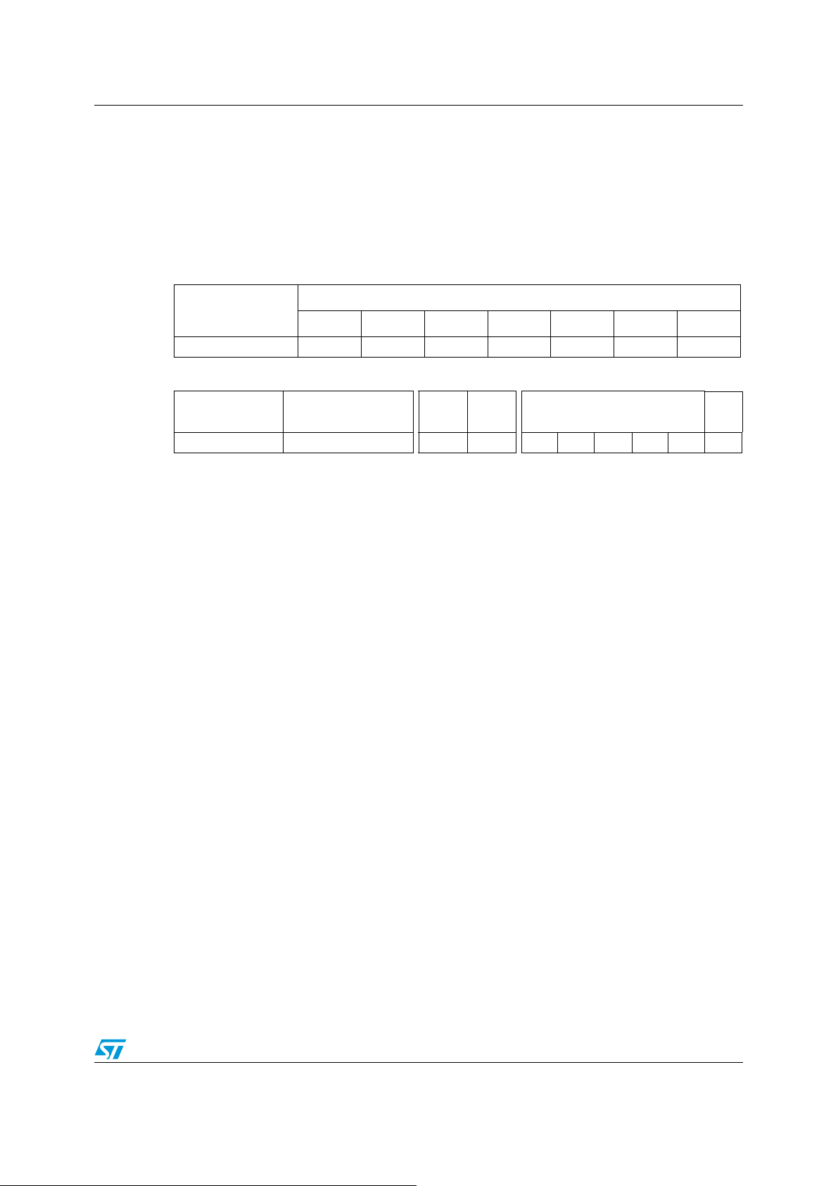
PM0044 STM8 instruction set
BREAK
Software break
BREAK
Syntax
Operation
Description In debug mode, the CPU is stalled and can be restarted by the debugger.
This instruction equals a NOP when the debugger is not connected.
Instruction overview
mnem
VI1HI0NZC
SIM - 1 - 1 - - -
Affected condition flags
Detailed description
Addressing
mode
Inherent BREAK 1 1 8B ✗
Asm cy lgth Op-code(s) ST7
Doc ID 13590 Rev 3 83/162
Page 84

STM8 instruction set PM0044
BRES
Bit Reset
BRES
Syntax BRES dst,#pos pos = [0..7] e.g. BRES PADR,#6
Operation dst <= dst AND COMPLEMENT (2**pos)
Description Read the destination byte, reset the corresponding bit (bit position), and
write the result in destination byte. The destination is a memory byte. The
bit position is a constant. This instruction is fast, compact, and does not
affect any register. Very useful for boolean variable manipulation.
Instruction overview
mnem dst bit position
VI1HI0NZ C
BRES Mem #pos -------
Affected condition flags
Detailed description
dst pos = 0..7 Asm cy lgth Op-code(s) ST7
longmem n=1+2*pos BRES $1000,#7 1 4 72 1n MS LS
See also: BSET
84/162 Doc ID 13590 Rev 3
Page 85

PM0044 STM8 instruction set
BSET
Bit Set
BSET
Syntax BSET dst,#pos pos = [0..7] e.g. BSET PADR,#7
Operation dst <= dst OR (2**pos)
Description Read the destination byte, set the corresponding bit (bit position), and write
the result in destination byte. The destination is a memory byte. The bit
position is a constant. This instruction is fast, compact, and does not affect
any register. Very useful for boolean variable manipulation.
Instruction overview
mnem dst bit position
VI1HI0NZ C
BSET Mem #pos -------
Affected condition flags
Detailed description
dst pos = 0..7 Asm cy lgth Op-code(s) ST7
longmem n=2*pos BSET $1000,#1 1 4 72 1n MS LS
See also: BRES
Doc ID 13590 Rev 3 85/162
Page 86

STM8 instruction set PM0044
BTJF
Bit Test and Jump if False
BTJF
Syntax BTJF dst,#pos,rel pos = [0..7], rel is relative jump label
e.g.: BTJFPADR,#3,skip
Operation PC = PC+lgth
PC = PC + rel IF (dst AND (2**pos)) = 0
Description Read the destination byte, test the corresponding bit (bit position), and
jump to 'rel' label if the bit is false (0), else continue the program to the next
instruction. The tested bit is saved in the C flag. The destination is a
memory byte. The bit position is a constant. The jump label represents a
signed offset to be added to the current PC/instruction address (relative
jump). This instruction is used for boolean variable manipulation, hardware
register flag tests, or I/O polling. This instruction is fast, compact, and does
not affect any registers. Very useful for boolean variable manipulation.
Instruction overview
mnem dst bit position jump label
BTJF Mem #pos rel ------C
Affected condition flags
VI1HI0NZ C
C ⇒Tested bit is saved in the C flag.
Detailed description
dst pos = 0..7 Asm cy lgth Op-code(s) ST7
longmem n = 1+2*pos
BTJF
$1000,#1,loop
2/3 5 72 0n MS LS XX
See also: BTJT
86/162 Doc ID 13590 Rev 3
Page 87

PM0044 STM8 instruction set
BTJT
Bit Test and Jump if True
BTJT
Syntax BTJT dst,#pos,rel pos = [0..7], rel is relative jump label
e.g.: BTJT PADR,#7,skip
Operation PC = PC+lgth
PC = PC + rel IF (dst AND (2**pos)) <> 0
Description Read the destination byte, test the corresponding bit (bit position), and
jump to 'rel' label if the bit is true (1), else continue the program to the next
instruction. The tested bit is saved in the C flag. The destination is a
memory byte. The bit position is a constant. The jump label represents a
signed offset to be added to the current PC/instruction address (relative
jump). This instruction is used for boolean variable manipulation, hardware
register flag tests, or I/O polling.
Instruction overview
mnem dst bit position jump label
BTJT Mem #pos rel ------C
Affected condition flags
VI1HI0NZ C
C ⇒ Tested bit is saved in the C flag.
Detailed description
dst pos = 0..7 Asm cy lgth Op-code(s) ST7
longmem n= 2*pos
BTJT
$1000,#1,loop
2/3 5 72 0n MS LS XX
See also: BTJF
Doc ID 13590 Rev 3 87/162
Page 88

STM8 instruction set PM0044
CALL
CALL Subroutine
CALL
(Absolute)
Operation PC = PC+lgth
(SP--) = PCL
(SP--) = PCH
PC = dst
Description The current PC register value is pushed onto the stack, then PC is loaded
with the destination address in same section of memory. The CALL
destination and the instruction following the CALL should be in the same
section as PCE is not stacked. The corresponding RET instruction should
be executed in the same section. This instruction should be used versus
CALLR when developing a program.
Instruction overview
mnem dst
VI1HI0NZC
CALL Mem -------
Affected condition flags
Detailed description
dst Asm cy lgth Op-code(s) ST7
longmem CALL $1000 4 3 CD MS LS ✗
(X) CALL(X) 4 1 FD ✗
(shortoff,X) CALL($10,X) 4 2 ED XX ✗
(longoff,X) CALL($1000,X) 4 3 DD MS LS ✗
(Y) CALL(Y) 4 2 90 FD ✗
(shortoff,Y) CALL($10,Y) 4 3 90 ED XX ✗
(longoff,Y) CALL($1000,Y) 4 4 90 DD MS LS ✗
[shortptr.w] CALL[$10.w] 6 3 92 CD XX ✗
[longptr.w] CALL[$1000.w] 6 4 72 CD MS LS
([shortptr.w],X) CALL([$10.w],X) 6 3 92 DD XX ✗
([longptr.w],X) CALL([$1000.w],X) 6 4 72 DD MS LS
([shortptr.w],Y) CALL([$10.w],Y) 6 3 91 DD XX ✗
See also:RET, CALLR, CALLF
88/162 Doc ID 13590 Rev 3
Page 89

PM0044 STM8 instruction set
CALLF
CALL Far Subroutine
CALLF
Syntax CALLF dst e.g. CALLF label
Operation PC = PC+lgth
(SP--) = PCL
(SP--) = PCH
(SP--) = PCE
PC = dst
Description The current PC register value is pushed onto the stack, then PC is loaded
with the destination address.This instruction is used with extended memory
addresses. For safe memory usage, a function which crosses sections
must be called by CALLF.
Instruction overview
mnem dst
VI1HI0NZC
CALLF Mem -------
Affected condition flags
Detailed description
dst Asm cy lgth Op-code(s) ST7
extmem CALLF $35AA00 5 4 8D ExtB MS LS
[longptr.e] CALLF [$2FFC.e] 8 4 92 8D MS LS
See also: RETF, CALL, JPF
Doc ID 13590 Rev 3 89/162
Page 90

STM8 instruction set PM0044
CALLR
CALL Subroutine Relative
CALLR
Syntax CALLR dst e.g. CALLR chk_pol
Operation PC = PC+lgth
(SP--) = PCL
(SP--) = PCH
PC = PC + dst
Description The current PC register value is pushed onto the stack, then PC is loaded
with the relative destination address. This instruction is used, once a
program is debugged, to shrink the overall program size. The CALLR
destination and the corresponding RET instruction address must be in the
same section, as PCE is not stacked.
Instruction overview
mnem dst
VI1HI0NZC
CALLR Mem -------
Affected condition flags
Detailed description
dst Asm cy lgth Op-code(s) ST7
shortmem CALLR $10 4 2 AD XX ✗
See also: CALL, RET
90/162 Doc ID 13590 Rev 3
Page 91

PM0044 STM8 instruction set
CCF
Complement Carry Flag
CCF
Syntax CCF
Operation CC.C <- CC.
C
Description Complements the Carry flag of the Condition Code (CC) register.
Instruction overview
Affected condition flags
C =C
mnem
VI1HI0NZC
CCF ------
,
Complements the carry flag of the CC register.
Detailed description
Addressing
mode
Inherent CCF 1 1 8C
Asm cy lgth Op-code(s) ST7
See also: RCF, SCF
C
Doc ID 13590 Rev 3 91/162
Page 92
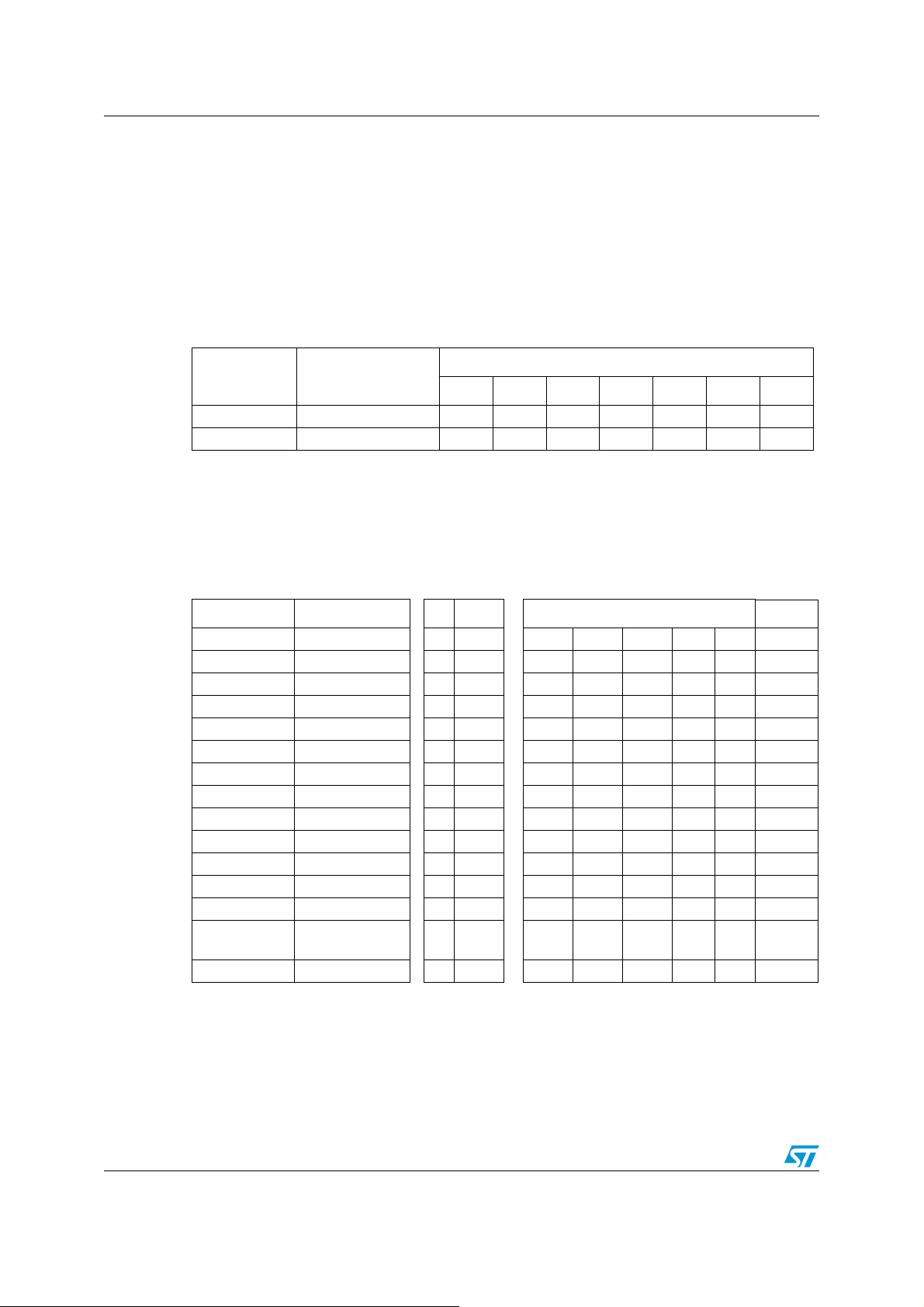
STM8 instruction set PM0044
CLR
Clear
CLR
Syntax CLR dst e.g. CLR A
Operation dst <= 00
Description The destination byte is forced to 00 value. The destination is either a
memory byte location or the accumulator. This instruction is compact, and
does not affect any register when used with RAM variables.
Instruction overview
mnem dst
VI1HI0NZ C
CLR Mem ----01-
CLR A 0 1
Affected condition flags
N: 0
Cleared
Z: 1
Set
Detailed description
dst Asm cy lgth Op-code(s) ST7
ACLR A 11 4F ✗
shortmem CLR $10 1 2 3F XX ✗
longmem CLR $1000 1 4 72 5F MS LS
(X) CLR (X) 1 1 7F ✗
(shortoff.X) CLR ($10,X) 1 2 6F XX ✗
(longoff,X) CLR ($1000,X) 1 4 72 4F MS LS
(Y) CLR (Y) 1 2 90 7F ✗
(shortoff,Y) CLR ($10,Y) 1 3 90 6F XX ✗
(longoff,Y) CLR ($1000,Y) 1 4 90 4F MS LS
(shortoff,SP) CLR ($10,SP) 1 2 0F XX
[shortptr.w] CLR [$10] 4 3 92 3F XX ✗
[longptr.w] CLR [$1000].w 4 4 72 3F MS LS
([shortptr.w],X) CLR ([$10],X) 4 3 92 6F XX ✗
([longptr.w].X]
([shortptr.w],Y) CLR ([$10],Y) 4 3 91 6F XX ✗
CLR
([$1000.w],X)
4 4 72 6F MS LS
See also: LD
92/162 Doc ID 13590 Rev 3
Page 93

PM0044 STM8 instruction set
CLRW
Clear word
CLRW
Syntax CLRW dst e.g. CLRW X
Operation dst <= 00
Description The destination is forced to 0000 value. The destination is an index
register.
Instruction overview
mnem dst
VI1HI0NZC
CLRW X - - - - 0 1 -
CLRW Y - - - - 0 1 -
Affected condition flags
N: 0
Cleared
Z: 1
Set
Detailed description
dst Asm cy lgth Op-code(s) ST7
XCLRW X 11 5F
YCLRW Y 12 905F
See also: LD
Doc ID 13590 Rev 3 93/162
Page 94

STM8 instruction set PM0044
CP
Compare
CP
Syntax CP dst,src e.g. CP A,(tbl,X)
Operation {N, Z, C} = Test (dst - src)
Description The source byte is subtracted from the destination byte and the result
is lost. However, N, Z, C flags of Condition Code (CC) register are updated
according to the result.The destination is a register, and the source is a
memory or data byte. This instruction generally is used just before a
conditional jump instruction.
Instruction overview
mnem dst src
CP Reg Mem V - - - N Z C
V ⇒ (A7
.M7 + A7.R7 + A7.M7.R7) ⊕ (A6.M6 + A6.R6 + A6.M6.R6)
VI1HI0N ZC
Affected condition flags
Set if the signed subtraction of the destination (dst) value from the
source (src) value generates a signed overflow (signed result cannot be
represented on 8 bits).
N ⇒ R7
Set if bit 7 of the result is set (negative value), cleared otherwise.
Z ⇒ R7
.R6.R5.R4.R3.R2.R1.R0
Set if the result is zero (0x00), cleared otherwise.
C ⇒ (A7
.M7 + A7.R7 + A7.M7.R7)
Set if the unsigned value of the contents of source (src) is larger than the
unsigned value of the destination (dst), cleared otherwise.
Detailed description
dst src Asm cy lgth Op-code(s) ST7
A #byte CP A,#$10 1 2 A1 XX ✗
A shortmem CP A,$10 1 2 B1 XX ✗
A longmem CP A,$1000 1 3 C1 MS LS ✗
A(X) CP A,(X) 1 1 F1 ✗
A (shortoff,X) CP A,($10,X) 1 2 E1 XX ✗
A (longoff,X) CP A,($1000,X) 1 3 D1 MS LS ✗
A(Y) CP A,(Y) 1 2 90 F1 ✗
A (shortoff,Y) CP A,($10,Y) 1 3 90 E1 XX ✗
A (longoff,Y) CP A,($1000,Y) 1 4 90 D1 MS LS ✗
A (shortoff,SP) CP A,($10,SP) 1 2 11 XX
A [shortptr.w] CP A,[$10.w] 4 3 92 C1 XX ✗
A [longptr.w] CP A,[$1000.w] 4 4 72 C1 MS LS
A ([shortptr.w],X) CP A,([$10.w],X) 4 3 92 D1 XX ✗
A ([longptr.w],X) CP A,([$1000.w],X) 4 4 72 D1 MS LS
A ([shortptr.w],Y) CP A,([$10.w],Y) 4 3 91 D1 XX ✗
See also: CPW, TNZ, BCP
94/162 Doc ID 13590 Rev 3
Page 95
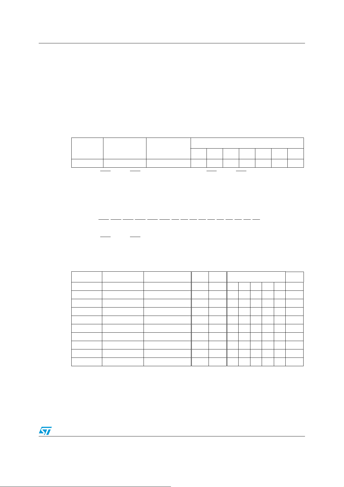
PM0044 STM8 instruction set
CPW
Compare word
CPW
Syntax CPW dst,src e.g. CPW Y,(tbl,X)
Operation {N, Z, C} = Test (dst - src)
Description The source byte is subtracted from the destination byte and the result is
lost. However, N, Z, C flags of Condition Code (CC) register are updated
according to the result. The destination is an index register, and the source
is a memory or data word. This instruction generally is used just before a
conditional jump instruction.
Instruction overview
mnem dst src
CPW Reg Mem V---NZC
V ⇒ (X15
.M15 + X15.R15 + X15.M15.R15) ⊕ (X14.M14 + X14.R14 + X14.M14.R14)
VI1HI0NZ C
Affected condition flags
Set if the signed subtraction of the destination (dst) value from the source (src)
value generates a signed overflow (signed result cannot be represented on 16
bits).
N ⇒ R15
Set if bit 7 of the result is set (negative value), cleared otherwise.
Z ⇒ R15
.R14.R13.R12.R11.R10.R9.R8.R7.R6.R5.R4.R3.R2.R1.R0
Set if the result is zero (0x00), cleared otherwise.
C ⇒ (X15
.M15 + X15.R15 + X15.M15.R15)
Set if the unsigned value of the contents of source (src) is larger than the
unsigned value of the destination (dst), cleared otherwise.
Detailed description
dst src Asm cy lgth Op-code(s) ST7
X #word CPW X,#$10 2 3 A3 MS LS ✗
X shortmem CPW X,$10 2 2 B3 XX ✗
X longmem CPW X,$1000 2 3 C3 MS LS ✗
X(Y) CPW X,(Y) 2290F3 ✗
X (shortoff,Y) CPW X,($10,Y) 2 3 90 E3 XX ✗
X (longoff,Y) CPW X,($1000,Y) 2 4 90 D3 MS LS ✗
X (shortoff,SP) CPW X,($10,SP) 2 2 13 XX
X [shortptr.w] CPW X,[$10.w] 5 3 92 C3 XX ✗
X [longptr.w] CPW X,[$1000.w] 5 4 72 C3 MS LS
X ([shortptr.w],Y) CPW X,([$10.w],Y) 5 3 91 D3 XX ✗
Doc ID 13590 Rev 3 95/162
Page 96

STM8 instruction set PM0044
CPW detailed description (Continued)
dst src Asm cy lgth Op-code(s) ST7
Y #word CPW Y,#$10 2 4 90 A3 MS LS ✗
Y shortmem CPW Y,$10 2 3 90 B3 XX ✗
Y longmem CPW Y,$1000 2 4 90 C3 MS LS ✗
Y(X) CPW Y,(X) 2 1 F3 ✗
Y (shortoff,X) CPW Y,($10,X) 2 2 E3 XX ✗
Y (longoff,X) CPW Y,($1000,X) 2 3 D3 MS LS ✗
Y [shortptr.w] CPW Y,[$10.w] 5 3 91 C3 XX ✗
Y ([shortptr.w],X) CPW Y,([$10.w],X) 5 3 92 D3 XX ✗
Y ([longptr.w],X) CPW Y,([$1000.w],X) 5 4 72 D3 MS LS
Note: CPW Y, (shortoff, SP) is not implemented, but can be emulated through a macro using
EXGW X,Y
& CPW X, (shortoff, SP)
See also: CP, TNZW, BCP
96/162 Doc ID 13590 Rev 3
Page 97

PM0044 STM8 instruction set
CPL
Logical 1’s Complement
CPL
Syntax CPL dst e.g. CPL (X)
Operation dst <= dst XOR FF, or FF - dst
Description The destination byte is read, then each bit is toggled (inverted) and the
result is written to the destination byte. The destination is either a memory
byte or a register. This instruction is compact, and does not affect any
registers when used with RAM variables.
Instruction overview
mnem dst
VI1HI0NZC
CPL Mem ----NZ1
CPL Reg ----NZ1
Affected condition flags
N ⇒ R7
Set if bit 7 of the result is set (negative value), cleared otherwise.
Z ⇒R7
.R6.R5.R4.R3.R2.R1.R0
Set if the result is zero (0x00), cleared otherwise.
C ⇒ 1
Set.
Detailed description
dst Asm cy lgth Op-code(s) ST7
ACPL A11 43 ✗
shortmem CPL$10 1 2 33 XX ✗
longmem CPL$1000 1 4 72 53 MS LS
(X) CPL(X) 1 1 73 ✗
(shortoff.X) CPL($10,X) 1 2 63 XX ✗
(longoff,X) CPL($1000,X) 1 4 72 43 MS LS
(Y) CPL(Y) 1 2 90 73 ✗
(shortoff,Y) CPL($10,Y) 1 3 90 63 XX ✗
(longoff,Y) CPL($1000,Y) 1 4 90 43 MS LS
(shortoff,SP) CPL($10,SP) 1 2 03 XX ✗
[shortptr.w] CPL[$10] 4 3 92 33 XX ✗
[longptr.w] CPL[$1000].w 4 4 72 33 MS LS
([shortptr.w],X) CPL([$10],X) 4 3 92 63 XX ✗
([longptr.w].X] CPL([$1000.w],X) 4 4 72 63 MS LS
([shortptr.w],Y) CPL([$10],Y) 4 3 91 63 XX ✗
See also: NEG, XOR, AND, OR
Doc ID 13590 Rev 3 97/162
Page 98

STM8 instruction set PM0044
CPLW
Logical 1’s Complement Word
CPLW
Syntax CPLW dst e.g. CPLW X
Operation dst <= dst XOR FFFF, or FFFF - dst
Description The destination index register is read, then each bit is toggled (inverted)
and the result is written back to the destination index register.
Instruction overview
mnem dst
VI1HI0NZC
CPLW Reg - - - - N Z 1
Affected condition flags
N ⇒ R15
Set if bit 7 of the result is set (negative value), cleared otherwise.
Z ⇒ R15
.R14.R13.R12.R11.R10.R9.R8.R7.R6.R5.R4.R3.R2.R1.R0
Set if the result is zero (0x00), cleared otherwise.
C ⇒ 1
Set
Detailed description
dst Asm cy lgth Op-code(s) ST7
XCPLW X21 53 ✗
YCPWL Y229053 ✗
See also: CPL, NEGW, XOR, AND, OR
98/162 Doc ID 13590 Rev 3
Page 99

PM0044 STM8 instruction set
DEC
Decrement
DEC
Syntax DEC dst
Operation dst <= dst - 1
Description The destination byte is read, then decremented by one, and the result is
written to the destination byte. The destination is either a memory byte or a
register. This instruction is compact, and does not affect any registers when
used with RAM variables.
Instruction overview
mnem dst
DEC Mem V - - - N Z -
DEC Reg V - - - N Z -
V ⇒ (A7.M7 + M7.R7
VI1HI0NZ C
+ R7.A7) ⊕ (A6.M6 + M6.R6 + R6.A6)
Affected condition flags
Set if the signed operation generates an overflow, cleared otherwise.
N ⇒ R7
Set if bit 7 of the result is set (negative value), cleared otherwise.
Z ⇒ R7
.R6.R5.R4.R3.R2.R1.R0
Set if the result is zero (0x00), cleared otherwise.
Detailed description
dst Asm cy lgth Op-code(s) ST7
ADEC A 1 1 4A ✗
shortmem DEC $10 1 2 3A XX ✗
longmem DEC $1000 1 4 72 5A MS LS
(X) DEC(X) 1 1 7A ✗
(shortoff.X) DEC($10,X) 1 2 6A XX ✗
(longoff,X) DEC($1000,X) 1 4 72 4A MS LS
(Y) DEC(Y) 1 2 90 7A ✗
(shortoff,Y) DEC($10,Y) 1 3 90 6A XX ✗
(longoff,Y) DEC($1000,Y) 1 4 90 4A MS LS
(shortoff,SP) DEC($10,SP) 1 2 0A XX
[shortptr.w] DEC[$10] 4 3 92 3A XX ✗
[longptr.w] DEC[$1000].w 4 4 72 3A MS LS
([shortptr.w],X) DEC([$10],X) 4 3 92 6A XX ✗
([longptr.w].X] DEC([$1000.w],X) 4 4 72 6A MS LS
([shortptr.w],Y) DEC([$10],Y) 4 3 91 6A XX ✗
See also: DECW, INC
Doc ID 13590 Rev 3 99/162
Page 100

STM8 instruction set PM0044
DECW
Decrement word
DECW
Syntax DECW dst
Operation dst <= dst - 1
Description The value of the destination index register is decremented by one.
Instruction overview
mnem dst
DECW Reg V - - - N Z -
V ⇒ (A15.M15 + M15.R15
VI1HI0NZC
+ R15.A15) ⊕ (A14.M14 + M14.R14 + R14.A14)
Affected condition flags
Set if the signed operation generates an overflow, cleared otherwise.
N ⇒ R15
Set if bit 15 of the result is set (negative value), cleared otherwise.
Z ⇒ R15
.R14.R13.R12.R11.R10.R9.R8.R7.R6.R5.R4.R3.R2.R1.R0
Set if the result is zero (0x0000), cleared otherwise.
Detailed description
dst Asm cy lgth Op-code(s) ST7
XDECW X 1 1 5A
YDECW Y 1 2 905A
See also: INCW, DEC
100/162 Doc ID 13590 Rev 3
 Loading...