

STMicroelectronics M93S66, M93S56, M93S46 User Manual
4Kbit, 2K bi t and 1Kb i t (16-bit wide)
MICROWIRE Serial Access EEPROM with Block Protection
FEAT URES SUM MARY
■ Industry Standard MICROWIRE Bus
■ Single Supply Voltage:
– 4.5 to 5.5V for M93Sx6
– 2.5 to 5.5V for M93Sx6-W
– 1.8 to 5.5V for M93Sx6-R
■ Single Organization: by Word (x16)
■ Programming Instructions that work on: Word
or Entire Memory
■ Self-timed Programming Cycle with Auto-
Erase
■ User Defined Write Protected Area
■ Page Write Mode (4 words)
■ Ready/Busy Signal During Programming
■ Speed:
– 1MHz Clock Rate, 10ms Write Time
(Current product, identified by process
identification letter F or M)
– 2MHz Clock Rate, 5ms Write Time (New
Product, identified by process
identification letter W or G)
■ Sequential Read Operation
■ Enhanced ESD/Latch-Up Behavior
■ More than 1 Million Erase/Write Cycles
■ More than 40 Year Data Retention
M93S66, M93S56
M93S46
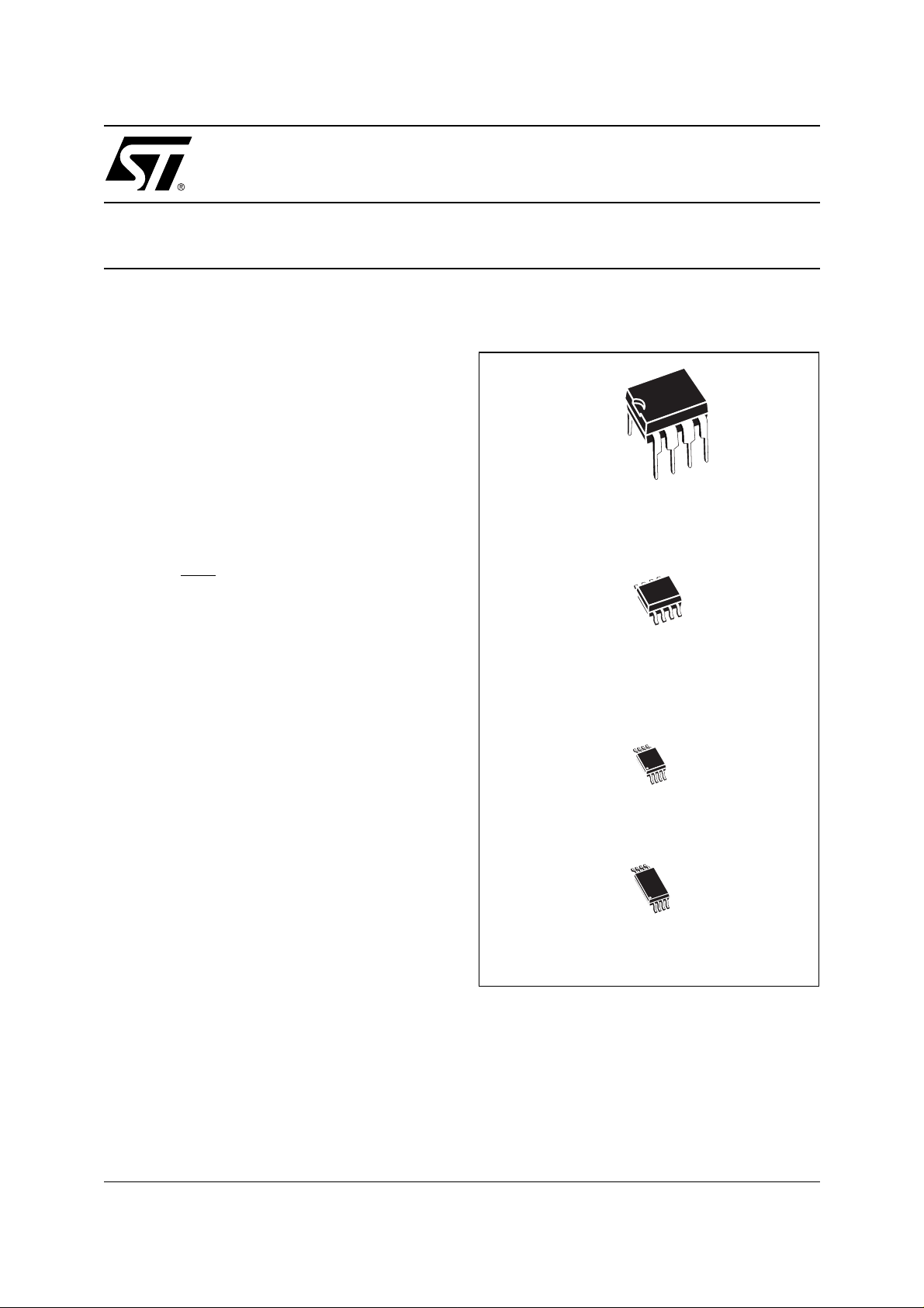
Figure 1. Packages
8
1
PDIP8 (BN)
8
1
SO8 (MN)
150 mil width
TSSOP8 (DS)
3x3mm body size
TSSOP8 (DW)
169 mil width
1/34April 2004

M93S66, M93S56, M93S46
TABLE OF CONTENTS
FEATURES SUMMARY . . . . . . . . . . . . . . . . . . . . . . . . . . . . . . . . . . . . . . . . . . . . . . . . . . . . . . . . . . . . . 1
Figure 1. Packages. . . . . . . . . . . . . . . . . . . . . . . . . . . . . . . . . . . . . . . . . . . . . . . . . . . . . . . . . . . . . . 1
SUMMARY DESCRIPTION. . . . . . . . . . . . . . . . . . . . . . . . . . . . . . . . . . . . . . . . . . . . . . . . . . . . . . . . . . . 4
Figure 2. Logic Diagram . . . . . . . . . . . . . . . . . . . . . . . . . . . . . . . . . . . . . . . . . . . . . . . . . . . . . . . . . . 4
Table 1. Signal Names . . . . . . . . . . . . . . . . . . . . . . . . . . . . . . . . . . . . . . . . . . . . . . . . . . . . . . . . . . 4
Figure 3. DIP, SO and TSSOP Connections . . . . . . . . . . . . . . . . . . . . . . . . . . . . . . . . . . . . . . . . . . 4
POWER-ON DATA PROTECTION . . . . . . . . . . . . . . . . . . . . . . . . . . . . . . . . . . . . . . . . . . . . . . . . . . . . .5
INSTRUCTIONS . . . . . . . . . . . . . . . . . . . . . . . . . . . . . . . . . . . . . . . . . . . . . . . . . . . . . . . . . . . . . . . . . . . 5
Table 2. Instruction Set for the M93S46 . . . . . . . . . . . . . . . . . . . . . . . . . . . . . . . . . . . . . . . . . . . . .6
Table 3. Instruction Set for the M93S66, M93S56. . . . . . . . . . . . . . . . . . . . . . . . . . . . . . . . . . . . . . 7
Figure 4. READ, WRITE, WEN and WDS Sequences . . . . . . . . . . . . . . . . . . . . . . . . . . . . . . . . . . . 8
Read . . . . . . . . . . . . . . . . . . . . . . . . . . . . . . . . . . . . . . . . . . . . . . . . . . . . . . . . . . . . . . . . . . . . . . . . . 9
Write Enable and Write Disable . . . . . . . . . . . . . . . . . . . . . . . . . . . . . . . . . . . . . . . . . . . . . . . . . . . 9
Write . . . . . . . . . . . . . . . . . . . . . . . . . . . . . . . . . . . . . . . . . . . . . . . . . . . . . . . . . . . . . . . . . . . . . . . . . 9
Figure 5. PAWRITE and WRAL Sequence. . . . . . . . . . . . . . . . . . . . . . . . . . . . . . . . . . . . . . . . . . . 10
Page Write . . . . . . . . . . . . . . . . . . . . . . . . . . . . . . . . . . . . . . . . . . . . . . . . . . . . . . . . . . . . . . . . . . . 10
Write All . . . . . . . . . . . . . . . . . . . . . . . . . . . . . . . . . . . . . . . . . . . . . . . . . . . . . . . . . . . . . . . . . . . . . 11
Figure 6. PREAD, PRWRITE and PREN Sequenc es. . . . . . . . . . . . . . . . . . . . . . . . . . . . . . . . . . . 12
Figure 7. PRCLEAR and PRDS Sequences. . . . . . . . . . . . . . . . . . . . . . . . . . . . . . . . . . . . . . . . . . 13
WRITE PROTECTION AND THE PROTECTION REGISTER . . . . . . . . . . . . . . . . . . . . . . . . . . . . . . . 14
Protection Register Read . . . . . . . . . . . . . . . . . . . . . . . . . . . . . . . . . . . . . . . . . . . . . . . . . . . . . . . 14
Protection Register Enable. . . . . . . . . . . . . . . . . . . . . . . . . . . . . . . . . . . . . . . . . . . . . . . . . . . . . . 14
Protection Register Clear. . . . . . . . . . . . . . . . . . . . . . . . . . . . . . . . . . . . . . . . . . . . . . . . . . . . . . . 1 4
Protection Register Write. . . . . . . . . . . . . . . . . . . . . . . . . . . . . . . . . . . . . . . . . . . . . . . . . . . . . . . 1 4
Protection Register Disable . . . . . . . . . . . . . . . . . . . . . . . . . . . . . . . . . . . . . . . . . . . . . . . . . . . . . 14
COMMON I/O OPERATION . . . . . . . . . . . . . . . . . . . . . . . . . . . . . . . . . . . . . . . . . . . . . . . . . . . . . . . . . 15
Figure 8. Write Sequence with One Clock Glitch . . . . . . . . . . . . . . . . . . . . . . . . . . . . . . . . . . . . . . 15
CLOCK PULSE COUNTER . . . . . . . . . . . . . . . . . . . . . . . . . . . . . . . . . . . . . . . . . . . . . . . . . . . . . . . . . 15
MAXIMUM RATING. . . . . . . . . . . . . . . . . . . . . . . . . . . . . . . . . . . . . . . . . . . . . . . . . . . . . . . . . . . . . . . . 16
Table 4. Absolute Maximum Ratings. . . . . . . . . . . . . . . . . . . . . . . . . . . . . . . . . . . . . . . . . . . . . . . 16
DC AND AC PARAMETERS. . . . . . . . . . . . . . . . . . . . . . . . . . . . . . . . . . . . . . . . . . . . . . . . . . . . . . . . . 17
Table 5. Operating Conditions (M93Sx6) . . . . . . . . . . . . . . . . . . . . . . . . . . . . . . . . . . . . . . . . . . . 17
Table 6. Operating Conditions (M93Sx6-W) . . . . . . . . . . . . . . . . . . . . . . . . . . . . . . . . . . . . . . . . . 17
Table 7. Operating Conditions (M93Sx6-R). . . . . . . . . . . . . . . . . . . . . . . . . . . . . . . . . . . . . . . . . . 17
Table 8. A C Measurem ent Condition s (M93Sx6 ) . . . . . . . . . . . . . . . . . . . . . . . . . . . . . . . . . . . . . 17
Table 9. A C Measurem ent Condition s (M93Sx6-W and M93Sx6-R). . . . . . . . . . . . . . . . . . . . . . . 17
2/34

M93S66, M93S56, M93S46
Figure 9. AC Testing Input Output Waveforms. . . . . . . . . . . . . . . . . . . . . . . . . . . . . . . . . . . . . . . . 18
Table 10.Capacitance. . . . . . . . . . . . . . . . . . . . . . . . . . . . . . . . . . . . . . . . . . . . . . . . . . . . . . . . . . . 18
Table 11. DC Characteristics (M93Sx6, Device Grade 6) . . . . . . . . . . . . . . . . . . . . . . . . . . . . . . . . 19
Table 12. DC Characteristics (M93Sx6, Device Grade 3) . . . . . . . . . . . . . . . . . . . . . . . . . . . . . . . . 19
Table 13. DC Characteristics (M93Sx6-W, Device Grade 6). . . . . . . . . . . . . . . . . . . . . . . . . . . . . . 20
Table 14. DC Characteristics (M93Sx6-W, Device Grade 3). . . . . . . . . . . . . . . . . . . . . . . . . . . . . . 21
Table 15. DC Characteristics (M93Sx6-R) . . . . . . . . . . . . . . . . . . . . . . . . . . . . . . . . . . . . . . . . . . . 21
Table 16. AC Characteristics (M93Sx6, Device Grade 6 or 3) . . . . . . . . . . . . . . . . . . . . . . . . . . . . 22
Table 17. AC Characteristics (M93Sx6-W, Device Grade 6). . . . . . . . . . . . . . . . . . . . . . . . . . . . . . 23
Table 18. AC Characteristics (M93Sx6-W, Device Grade 3). . . . . . . . . . . . . . . . . . . . . . . . . . . . . . 24
Table 19. AC Characteristics (M93Sx6-R). . . . . . . . . . . . . . . . . . . . . . . . . . . . . . . . . . . . . . . . . . . . 25
Figure 10.Synchronous Timing (Start and Op-Code Input). . . . . . . . . . . . . . . . . . . . . . . . . . . . . . . 26
Figure 11.Synchronous Timing (Read or Write) . . . . . . . . . . . . . . . . . . . . . . . . . . . . . . . . . . . . . . . 26
Figure 12.Synchronous Timing (Read or Write) . . . . . . . . . . . . . . . . . . . . . . . . . . . . . . . . . . . . . . . 27
PACKAGE MECHANICAL . . . . . . . . . . . . . . . . . . . . . . . . . . . . . . . . . . . . . . . . . . . . . . . . . . . . . . . . . . 28
Figure 13.PDIP8 – 8 pin Plastic DIP, 0.25mm lead frame, Package Outline . . . . . . . . . . . . . . . . .28
Table 20. PDIP8 – 8 pin Plastic DIP, 0.25mm lead frame, Package Mec hanical Data . . . . . . . . . . 28
Figure 14.SO8 narrow – 8 lead Plastic Small Outline, 150 mils body width, Package Outline . . . . 29
Table 21. SO8 narrow – 8 lead Plastic Small Outline, 150 mils body width, Package Mechanical Data
29
Figure 15.TSSOP8 3x3mm² – 8 lead Thin Shrink Small Outline, 3x3mm ² body size, Package Outline
30
Table 22. TSSOP8 3x3mm² – 8 lead Thin Shrink Small Outline, 3x3mm² body size, Mechanical Data
30
Figure 16.TSSOP8 – 8 lead Thin Shrink Small Outline, Package Outline . . . . . . . . . . . . . . . . . . . 31
Table 23. TSSOP8 – 8 lead Thin Shrink Sma ll Outline, Packag e Mechani cal Data . . . . . . . . . . . . 31
PART NUMBERING . . . . . . . . . . . . . . . . . . . . . . . . . . . . . . . . . . . . . . . . . . . . . . . . . . . . . . . . . . . . . . . 32
Table 24.Ordering Information Scheme . . . . . . . . . . . . . . . . . . . . . . . . . . . . . . . . . . . . . . . . . . . . . 32
Table 25. How to Identify Current and New Products by the Process Identification Letter . . . . . . . 32
REVISION HISTORY. . . . . . . . . . . . . . . . . . . . . . . . . . . . . . . . . . . . . . . . . . . . . . . . . . . . . . . . . . . . . . . 33
Table 26. Document Revision History. . . . . . . . . . . . . . . . . . . . . . . . . . . . . . . . . . . . . . . . . . . . . . . 33
3/34
M93S66, M93S56, M93S46
SUMMARY DESCRIPTION
This specification covers a range of 4K, 2K, 1K bit
serial Electrically Erasable Programmable Memory (EEPROM) products (respectively for M93S66,
M93S56, M93S46). In this text, these products are
collectively referred to as M93Sx6.
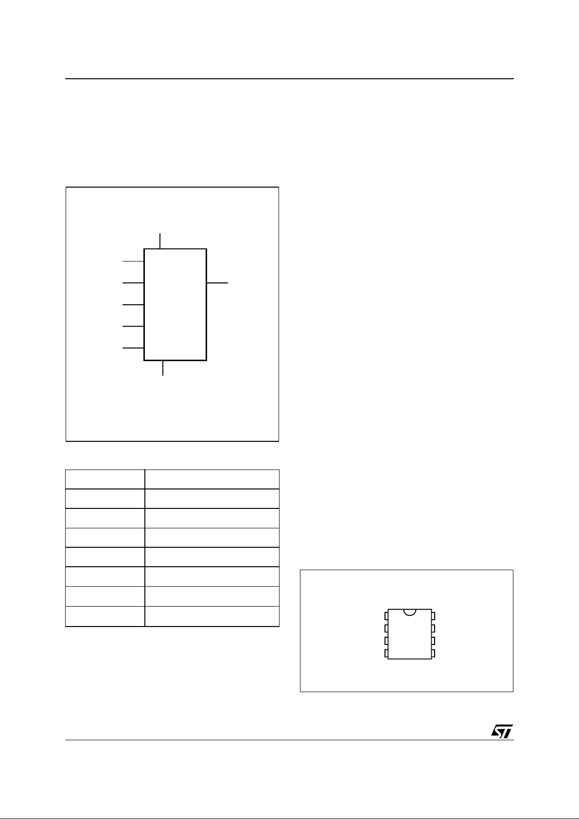
Figure 2. Logic Diagram
V
CC
D
C Q
S
PRE
W
Table 1. Signal Names
S Chip Select Input
D Serial Data Input
Q Serial Data Output
C Ser ial Clock
M93Sx6
V
SS
AI02020
and instructions used to set the memory protection. These are summarized in Table 2. and Table
3.).
A Read Data from Memory (READ) instruction
loads the address of the first word to be read into
an internal address pointer. The data contained at
this address is then clocked out serially. The address pointer is automatically incremented after
the data is output and, if the Chi p S elect In put (S)
is held High, the M93Sx6 can output a sequential
stream of data words. In this way, the memory can
be read as a data stream from 16 to 4096 bits (for
the M93S66), or continuously as the address
counter automatically rolls over to 0 0h when the
highest address is reached.
Within the time required by a programming cycle
), up to 4 words may be written with help of the
(t
W
Page Write instruction. the whole memory may
also be erased, or set to a predetermined pattern,
by using the Write All instruction.
Within the memory, a user defined area may be
protected against further Write instructions. The
size of this area is defined by the content of a Protection Register, located outside of the memory array. As a final protection step, data may be
permanently protected by programming a One
Time Programming bit (OTP bit) which lo cks the
Protection Register content.
Programming is internally s elf-timed (the external
clock signal on Serial Clock (C) may be stopped or
left running after the start of a Write cycle) and
does not require an erase cycle prior to the Write
instruction. The Write instruction writes 16 bits at a
time into one of the word locations of the M93Sx6,
the Page Write instruction writes up to 4 words of
16 bits to sequential locations, assum ing in both
cases that all addresses are outside the Write Protected area. After the start of the programming cycle, a Busy/Ready signal is available on Serial
Data Output (Q) when Chip Select Input (S) is driven High.
PRE Protection Register Enable
W Write Enable
V
CC
V
SS
Supply Voltage
Ground
The M93Sx6 is accessed through a serial input (D)
and output (Q) us in g t he M ICR OWI RE b us protocol. The memory is divided into 256, 128, 64 x16
bit words (respectively for M93S66, M93S56,
M93S46).
The M93Sx6 is accessed by a set of instructions
which includes Read, W rite, Page Write, Write A ll
4/34
Figure 3. DIP, SO and TSSOP Connections
M93Sx6
SV
1
2
D
3
Q
4
Note: See PACKAGE MECHANICAL section for package dimen-
sions, and how to ident i fy pi n-1.
8
7
6
5
AI02021
PREC
W
V
CC
SS

M93S66, M93S56, M93S46
An internal Power-on Data Protec tion m echani sm
in the M93Sx6 inhibits the device when the supply
is too low.
POWER-ON DATA PROTECTION
To prevent data corruption and inadvertent write
operations during power-up, a Power-On Reset
(POR) circuit resets all internal programming circuitry, and sets the device in the Write Disable
mode.
– At Power-up and Power-down, the device
must not be selected (that is, Chip Select Input
(S) must be driven Low) until the supply
voltage reaches the operating value V
specified in Table 5. to Table 6..
– When V
reaches its valid level, the device is
CC
properly reset (in the Write Disable mode) and
is ready to decode and execute incoming
instructions.
For the M93Sx6 devices (5V range) the POR
threshold voltage is around 3 V. For the M93S x6W (3V range) and M93Sx6-R (2V range) the POR
threshold voltage is around 1.5V.
CC
INSTRUCTIONS
The instruction set of the M93Sx6 devices contains seven instructions, as summarized in Table
2. to Table 3.. Each instruction co nsists of t he fol-
lowing parts, as shown in Figure 4.:
■ Each instruction is preceded by a rising edge
on Chip Select Input (S) with Serial Clock (C)
being held Low.
■ A start bit, which is the first ‘1’ read on Serial
Data Input (D) during the rising edge of Serial
Clock (C).
■ Two op-code bits, read on Serial Data Input
(D) during the rising edge of Serial Clock (C).
(Some instructions also use the first two bits of
the address to define the op-code).
■ The address bits of the byte or word that is to
be accessed. For the M93S46, the address is
made up of 6 bits (see Table 2.). Fo r t h e
M93S56 and M93S66, the address is made up
of 8 bits (see Table 3.).
The M93Sx6 devices are fabricated in CMOS
technology and are therefore able to run as slow
as 0 Hz (static input signals) or as fast as the maximum ratings specified in Table 16. to Table 19..
5/34

M93S66, M93S56, M93S46
Table 2. Instruction Set for the M93S46
Instruction Description W PRE
Start
bit
Op-
Code
Address
1
Data
Required
Clock
Cycles
Additional
Comments
READ
WRITE
PAWRITE
WRAL
WEN Write Enable 1 0 1 00 11 XXXX 9
WDS Write Disable X 0 1 00 00 XXXX 9
PRREAD
PRWRITE
PRCLEAR
Read Data
from Memory
Write Data to
Memory
Page Write to
Memory
Write All
Memory
with same
Data
Protection
Register Read
Protection
Register Write
Protection
Register Clear
X 0 1 10 A5-A0 Q15-Q0
1 0 1 01 A5-A0 D15-D0 25
10 1 11 A5-A0
10 1 0001 XXXXD15-D0 25
X 1 1 10 XXXXXX
11 1 01 A5-A0 9
1 1 1 11 111111 9
N x
D15-D0
Q5-Q0
+ Flag
9 + N x 16
Write is executed if
the address is not
inside the Protected
area
Write is executed if
all the N addresses
are not inside the
Protected area
Write all data if the
Protection Register
is cleared
Data Output =
Protection Register
content + Protection
Flag bit
Data above specified
address A5-A0 are
protected
Protect Flag is also
cleared (cleared
Flag = 1)
PREN
PRDS
Note: 1. X = Don’t Care bit.
6/34
Protection
Register
Enable
Protection
Register
Disable
1 1 1 00 11XXXX 9
1 1 1 00 000000 9
OTP bit is set
permanently

Table 3. Instruction Set for the M93S66, M93S56
Instruction Description W PRE
Start
bit
Op-
Code
Address
1,2
M93S66, M93S56, M93S46
Data
Required
Clock
Cycles
Additional
Comments
READ
WRITE
PAWRITE
Read Data
from Memory
Write Data to
Memory
Page Write to
Memory
X 0 1 10 A7-A0 Q15-Q0
1 0 1 01 A7-A0 D15-D0 27
10 1 11 A7-A0
N x
D15-D0
11 + N x 16
Write All
WRAL
Memory
with same
1 0 1 00 01XXXXXX D15-D0 27
Data
WEN Write Enable 1 0 1 00 11XXXXXX 11
WDS Write Disable X 0 1 00 00XXXXXX 11
PRREAD
PRWRITE
PRCLEAR
Protection
Register Read
Protection
Register Write
Protection
Register Clear
X 1 1 10 XXXXXXXX
11 1 01 A7-A0 11
1 1 1 11 11111111 11
Q7-Q0
+ Flag
Protection
PREN
Register
1 1 1 00 11XXXXXX 11
Enable
Write is executed if
the address is not
inside the
Protected area
Write is executed if
all the N
addresses are not
inside the
Protected area
Write all data if the
Protection
Register is cleared
Data Output =
Protection
Register content +
Protection Flag bit
Data above
specified address
A7-A0 are
protected
Prot ect Flag i s als o
cleared (cleared
Flag = 1)
PRDS
Register
1 1 1 00 00000000 11
Disable
Note: 1. X = Don’t Care bit.
2. Address bit A7 is not decoded by t he M 93S56.
Protection
OTP bit is set
permanently
7/34
M93S66, M93S56, M93S46
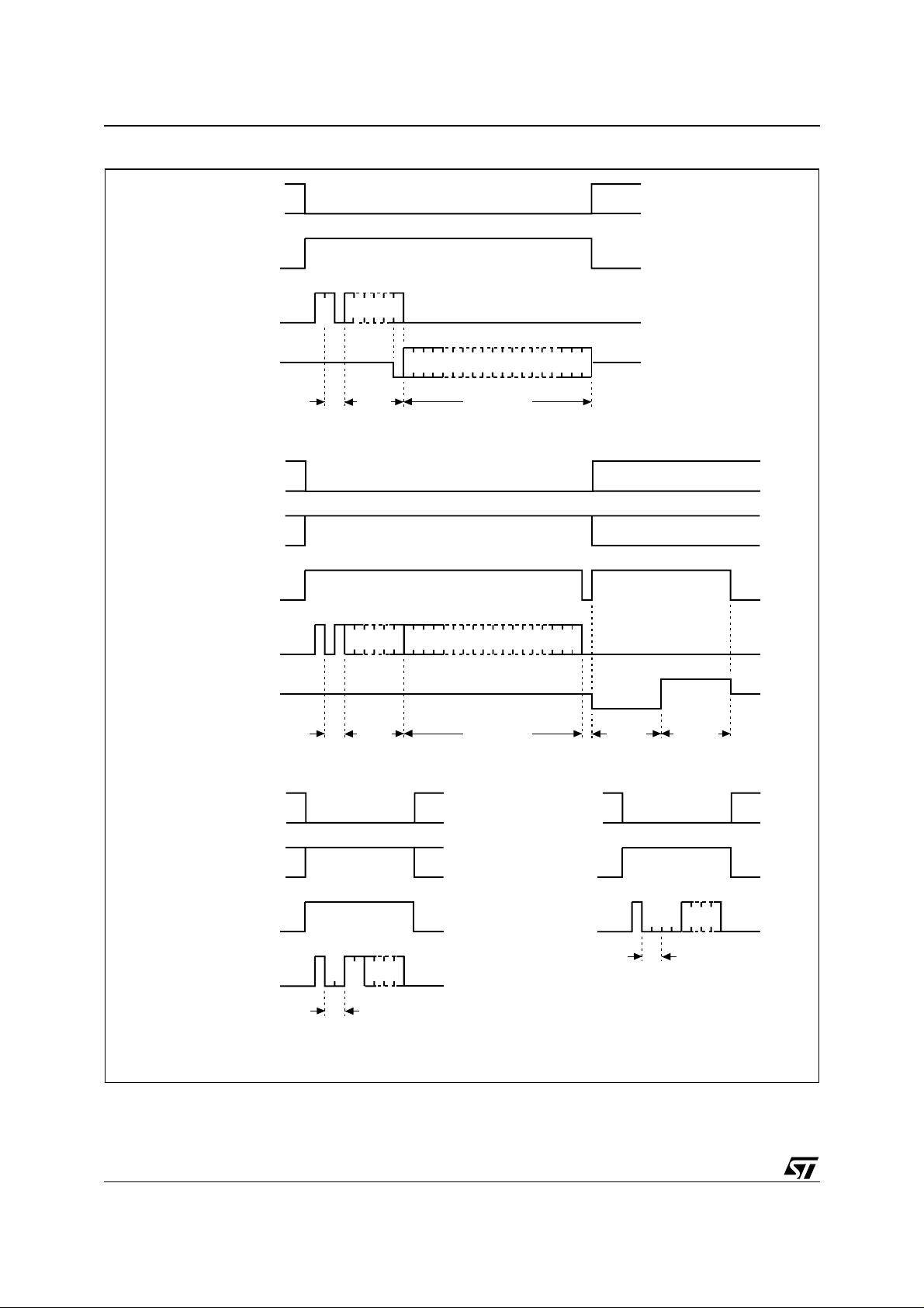
Figure 4. READ, WRITE, WEN and WDS Sequences
PREREAD
S
WRITE
D
Q
PRE
W
S
D
Q
1 1 0 An A0
ADDR
OP
CODE
1 0An A0
ADDR
OP
CODE
Qn Q0
DATA OUT
Dn D01
DATA IN
CHECK
STATUS
BUSY READY
WRITE
ENABLE
Note: For the meanings of An, Xn, Qn and Dn, see Table 2. and Table 3..
PRE
W
S
D
1
0XnX0
101
OP
CODE
8/34
WRITE
DISABLE
PRE
S
D
1
0XnX0
0 00
OP
CODE
AI00889D

M93S66, M93S56, M93S46
Read
The Read Data from Memory (READ) instruction
outputs serial data on Serial Data Output (Q).
When the instruction is received, the op-code and
address are decoded, and the data from the memory is transferred to an output shift register. A dummy 0 bit is output first, followed by the 16-bit word,
with the most significant bit first. Output data
changes are triggered b y the rising edge of Se rial
Clock (C). The M93Sx6 automatically incremen ts
the internal address register and clocks out the
next byte (or word) as long as the Chip Select Input (S) is held High. In this case, the dummy 0 bit
is not output between bytes (or words) and a continuous stream of data can be read.
Write Enable and Write Disable
The Write Enable (WEN) instruction enables the
future execution of write instructions, and the Write
Disable (WDS) instruction disables it. When power
is first app lied, the M93 S x 6 in i tializes itse lf so that
write instructions are disabled. After an Write Enable (WEN) instruction has been executed, writing
remains enabled until an Write Disable (WDS) instruction is executed, or until V
falls below the
CC
power-on reset threshold voltage . To protect the
memory contents from accidental corruption, it is
advisable to issue the Write Disable (WDS) instruction after every write cycle. The Read Data
from Memory (READ) instruction is not affected by
the Write Enable (WEN) or Write Disable (WDS)
instructions.
Write
The Write Data to Memory (WRITE) instruction is
composed of the Start bit plus the op-code followed by the address and the 16 data bits to be
written.
Write Enable (W) must be held High before and
during the instruction. Input addres s and data, on
Serial Data Input (D) are sampled on the rising
edge of Serial Clock (C).
After the last data bit has been sampled, the C hip
Select Input (S) must be taken Low before the next
rising edge of Serial Clock (C). If Chip Select Input
(S) is brought Low before or after this specific time
frame, the self-timed programming cycle will not
be started, and the addressed location will not be
programmed.
While the M93Sx6 is performing a write cycle, but
after a delay (t
) before the status information
SLSH
becomes available, Chip S elect Input (S) can be
driven High to monitor the status of the write cycle:
Serial Data Output (Q) is driven Low while the
M93Sx6 is still busy, and High when the cycle is
complete, and the M93Sx6 is ready to receive a
new instruction. The M93Sx6 ignores any data on
the bus while it is busy on a wri te cycle. O nce t he
M93Sx6 is Ready, Serial Data Output (Q) is driven
High, and remains in this state until a new start bit
is decoded or the Chip Select I nput (S) is brought
Low.
Programming is internally self-timed, so the external Serial Clock (C) may be disconnected o r left
running after the start of a write cycle.
9/34
M93S66, M93S56, M93S46
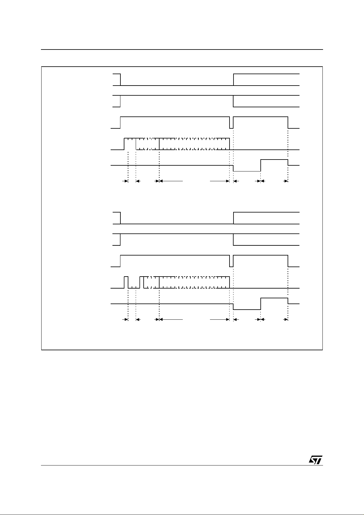
Figure 5. PA WR I TE and W R AL Sequen ce
PAGE WRITE
WRITE
ALL
PRE
W
S
D
Q
PRE
W
1 1An A0
ADDR
OP
CODE
CHECK
STATUS
Dn D01
DATA IN
BUSY READY
S
D
Q
Note: F or the mea ni ngs of An, Xn and Dn, please see Tabl e 2. and Table 3..
Page Write
A Page Write to Memory (PAWRITE) instruction
contains the first address to be written, followed by
up to 4 data words.
After the receipt of each data w ord, bits A1-A 0 of
the internal address regist er are increm ent ed, the
high order bits remaining unchanged (A7-A2 for
M93S66, M93S56; A5-A2 for M93S46). Users
must take care, in the software, to ensure that the
last word address has the same upper order address bits as the initial address transmitted to
avoid address roll-over.
01
1 0XnX0
ADDR
OP
CODE
Dn D00
DATA IN
The Page Write to Memory (PAWRITE) instruction
will not be executed if any of the 4 words addresses the protected area.
Write Enable (W) must be held High before and
during the instruction. Input addres s and data, on
Serial Data Input (D) are sampled on the rising
edge of Serial Clock (C).
After the last data bit has been sampled, the C hip
Select Input (S) must be taken Low before the next
rising edge of Serial Clock (C). If Chip Select Input
(S) is brought Low before or after this specific time
frame, the self-timed programming cycle will not
CHECK
STATUS
BUSY READY
AI00890C
10/34

M93S66, M93S56, M93S46
be started, and the addressed location will not be
programmed.
While the M93Sx6 is performing a write cycle, but
after a delay (t
) before the status information
SLSH
becomes available, Chip S elect Input (S) can be
driven High to monitor the status of the write cycle:
Serial Data Output (Q) is driven Low while the
M93Sx6 is still busy, and High when the cycle is
complete, and the M93Sx6 i s ready to receive a
new instruction. The M93Sx6 ignores any data on
the bus while it is busy on a wri te cycle. O nce t he
M93Sx6 is Ready, Serial Data Output (Q) is driven
High, and remains in this state until a new start bit
is decoded or the Chip Select I nput (S) is brought
Low.
Programming is internally self-timed, so the external Serial Clock (C) may be disconnected o r left
running after the start of a write cycle.
Writ e All
The Write All Memory with same Data (WRAL) instruction is valid only after the Protection Register
has been cleared by executing a Protection Register Clear (PRCLEAR) instruction. The Write All
Memor y with same Data (WRAL) instructi on simultaneously writes the whole memory with the same
data word given in the instruction.
Write Enable (W) must be held High before and
during the instruction. Input addres s and data, on
Serial Data Input (D) are sampled on the rising
edge of Serial Clock (C).
After the last data bit has been sampled, the C hip
Select Input (S) must be taken Low before the next
rising edge of Serial Clock (C). If Chip Select Input
(S) is brought Low before or after this specific time
frame, the self-timed programming cycle will not
be started, and the addressed location will not be
programmed.
While the M93Sx6 is performing a write cycle, but
after a delay (t
) before the status information
SLSH
becomes available, Chip S elect Input (S) can be
driven High to monitor the status of the write cycle:
Serial Data Output (Q) is driven Low while the
M93Sx6 is still busy, and High when the cycle is
complete, and the M93Sx6 is ready to receive a
new instruction. The M93Sx6 ignores any data on
the bus while it is busy on a wri te cycle. O nce t he
M93Sx6 is Ready, Serial Data Output (Q) is driven
High, and remains in this state until a new start bit
is decoded or the Chip Select I nput (S) is brought
Low.
Programming is internally self-timed, so the external Serial Clock (C) may be disconnected o r left
running after the start of a write cycle.
11/34
 Loading...