

STMicroelectronics M93C86, M93C76, M93C66, M93C56, M93C46 Technical data
16Kbit, 8Kbit, 4Kbit, 2Kbit and 1Kbit (8-bit or 16-bit wide)
FEATURES SUMMARY
M93C86, M93C76, M93C66
M93C56, M93C46
MICROWIRE® Serial Access EEPROM
■ Industry Standard MICROWIRE Bus
■ Single Supply Voltage:
– 4.5 to 5.5V for M93Cx6
– 2.5 to 5.5V for M93Cx6-W
– 1.8 to 5.5V for M93Cx6-R
■ Dual Organization: by Word (x16) or Byte (x8)
■ Programming Instructions that work on: Byte,
Word or Entire Memory
■ Self-timed Programming Cycle with Auto-
Erase: 5ms
■ Ready/Busy Signal During Programming
■ 2MHz Clock Rate
■ Sequential Read Operation
■ Enhanced ESD/Latch-Up Behavior
■ More than 1 Million Erase/Write Cycles
■ More than 40 Year Data Retention
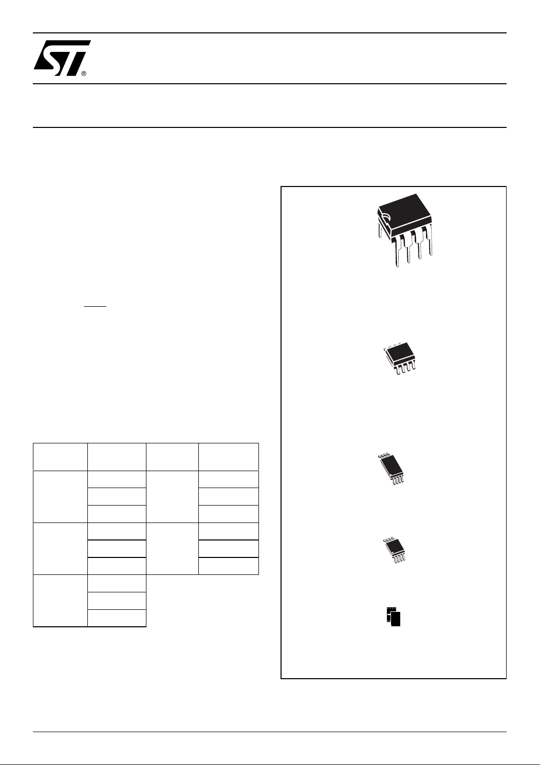
■ Packages
– ECOPACK® (RoHS compliant)
Table 1. Product List
Reference
M93C86
M93C76
M93C66
Part
Number
M93C86
M93C86-W M93C56-W
M93C86-R M93C56-R
M93C76
M93C76-W M93C46-W
M93C76-R M93C46-R
M93C66
M93C66-W
M93C66-R
Reference
M93C56
M93C46
Part
Number
M93C56
M93C46
Figure 1. Packages
8
1
PDIP8 (BN)
8
1
SO8 (MN)
150 mil width
TSSOP8 (DW)
169 mil width
TSSOP8 (DS)
3x3mm² body size (MSOP)
UFDFPN8 (MB)
2x3mm² (MLP)
1/31October 2005

M93C86, M93C76, M93C66, M93C56, M93C46
TABLE OF CONTENTS
FEATURES SUMMARY . . . . . . . . . . . . . . . . . . . . . . . . . . . . . . . . . . . . . . . . . . . . . . . . . . . . . . . . . . . . . 1
Table 1. Product List . . . . . . . . . . . . . . . . . . . . . . . . . . . . . . . . . . . . . . . . . . . . . . . . . . . . . . . . . . . . 1
Figure 1. Packages. . . . . . . . . . . . . . . . . . . . . . . . . . . . . . . . . . . . . . . . . . . . . . . . . . . . . . . . . . . . . . 1
Figure 2. Logic Diagram . . . . . . . . . . . . . . . . . . . . . . . . . . . . . . . . . . . . . . . . . . . . . . . . . . . . . . . . . . 4
Table 2. Signal Names . . . . . . . . . . . . . . . . . . . . . . . . . . . . . . . . . . . . . . . . . . . . . . . . . . . . . . . . . . 4
Table 3. Memory Size versus Organization. . . . . . . . . . . . . . . . . . . . . . . . . . . . . . . . . . . . . . . . . . . 4
Table 4. Instruction Set for the M93Cx6 . . . . . . . . . . . . . . . . . . . . . . . . . . . . . . . . . . . . . . . . . . . . .4
Figure 3. DIP, SO, TSSOP and MLP Connections (Top View). . . . . . . . . . . . . . . . . . . . . . . . . . . . . 5
MEMORY ORGANIZATION . . . . . . . . . . . . . . . . . . . . . . . . . . . . . . . . . . . . . . . . . . . . . . . . . . . . . . . . . . 6
INTERNAL DEVICE RESET . . . . . . . . . . . . . . . . . . . . . . . . . . . . . . . . . . . . . . . . . . . . . . . . . . . . . . . . . . 6
ACTIVE POWER AND STANDBY POWER MODES . . . . . . . . . . . . . . . . . . . . . . . . . . . . . . . . . . . . . . . 6
INSTRUCTIONS . . . . . . . . . . . . . . . . . . . . . . . . . . . . . . . . . . . . . . . . . . . . . . . . . . . . . . . . . . . . . . . . . . . 7
Table 5. Instruction Set for the M93C46 . . . . . . . . . . . . . . . . . . . . . . . . . . . . . . . . . . . . . . . . . . . . .7
Table 6. Instruction Set for the M93C56 and M93C66 . . . . . . . . . . . . . . . . . . . . . . . . . . . . . . . . . . 8
Table 7. Instruction Set for the M93C76 and M93C86 . . . . . . . . . . . . . . . . . . . . . . . . . . . . . . . . . . 8
Read . . . . . . . . . . . . . . . . . . . . . . . . . . . . . . . . . . . . . . . . . . . . . . . . . . . . . . . . . . . . . . . . . . . . . . . . . 9
Erase/Write Enable and Disable. . . . . . . . . . . . . . . . . . . . . . . . . . . . . . . . . . . . . . . . . . . . . . . . . . . 9
Figure 4. READ, WRITE, EWEN, EWDS Sequences. . . . . . . . . . . . . . . . . . . . . . . . . . . . . . . . . . . . 9
Erase. . . . . . . . . . . . . . . . . . . . . . . . . . . . . . . . . . . . . . . . . . . . . . . . . . . . . . . . . . . . . . . . . . . . . . . . 10
Write . . . . . . . . . . . . . . . . . . . . . . . . . . . . . . . . . . . . . . . . . . . . . . . . . . . . . . . . . . . . . . . . . . . . . . . . 10
Figure 5. ERASE, ERAL Sequences . . . . . . . . . . . . . . . . . . . . . . . . . . . . . . . . . . . . . . . . . . . . . . . 10
Erase All . . . . . . . . . . . . . . . . . . . . . . . . . . . . . . . . . . . . . . . . . . . . . . . . . . . . . . . . . . . . . . . . . . . . . 11
Write All . . . . . . . . . . . . . . . . . . . . . . . . . . . . . . . . . . . . . . . . . . . . . . . . . . . . . . . . . . . . . . . . . . . . . 11
Figure 6. WRAL Sequence . . . . . . . . . . . . . . . . . . . . . . . . . . . . . . . . . . . . . . . . . . . . . . . . . . . . . . . 11
READY/BUSY STATUS . . . . . . . . . . . . . . . . . . . . . . . . . . . . . . . . . . . . . . . . . . . . . . . . . . . . . . . . . . . . 12
INITIAL DELIVERY STATE. . . . . . . . . . . . . . . . . . . . . . . . . . . . . . . . . . . . . . . . . . . . . . . . . . . . . . . . . . 12
COMMON I/O OPERATION . . . . . . . . . . . . . . . . . . . . . . . . . . . . . . . . . . . . . . . . . . . . . . . . . . . . . . . . . 12
CLOCK PULSE COUNTER . . . . . . . . . . . . . . . . . . . . . . . . . . . . . . . . . . . . . . . . . . . . . . . . . . . . . . . . . 12
Figure 7. Write Sequence with One Clock Glitch . . . . . . . . . . . . . . . . . . . . . . . . . . . . . . . . . . . . . . 12
MAXIMUM RATING. . . . . . . . . . . . . . . . . . . . . . . . . . . . . . . . . . . . . . . . . . . . . . . . . . . . . . . . . . . . . . . . 13
Table 8. Absolute Maximum Ratings. . . . . . . . . . . . . . . . . . . . . . . . . . . . . . . . . . . . . . . . . . . . . . . 13
DC AND AC PARAMETERS. . . . . . . . . . . . . . . . . . . . . . . . . . . . . . . . . . . . . . . . . . . . . . . . . . . . . . . . . 14
Table 9. Operating Conditions (M93Cx6) . . . . . . . . . . . . . . . . . . . . . . . . . . . . . . . . . . . . . . . . . . . 14
Table 10. Operating Conditions (M93Cx6-W) . . . . . . . . . . . . . . . . . . . . . . . . . . . . . . . . . . . . . . . . . 14
Table 11. Operating Conditions (M93Cx6-R) . . . . . . . . . . . . . . . . . . . . . . . . . . . . . . . . . . . . . . . . . 14
2/31

M93C86, M93C76, M93C66, M93C56, M93C46
Table 12. AC Measurement Conditions (M93Cx6) . . . . . . . . . . . . . . . . . . . . . . . . . . . . . . . . . . . . . 15
Table 13. AC Measurement Conditions (M93Cx6-W and M93Cx6-R) . . . . . . . . . . . . . . . . . . . . . . 15
Figure 8. AC Testing Input Output Waveforms. . . . . . . . . . . . . . . . . . . . . . . . . . . . . . . . . . . . . . . . 15
Table 14. Capacitance. . . . . . . . . . . . . . . . . . . . . . . . . . . . . . . . . . . . . . . . . . . . . . . . . . . . . . . . . . . 15
Table 15. DC Characteristics (M93Cx6, Device Grade 6). . . . . . . . . . . . . . . . . . . . . . . . . . . . . . . . 16
Table 16. DC Characteristics (M93Cx6, Device Grade 7 or 3) . . . . . . . . . . . . . . . . . . . . . . . . . . . . 16
Table 17. DC Characteristics (M93Cx6-W, Device Grade 6) . . . . . . . . . . . . . . . . . . . . . . . . . . . . . 17
Table 18. DC Characteristics (M93Cx6-W, Device Grade 7 or 3) . . . . . . . . . . . . . . . . . . . . . . . . . . 18
Table 19. DC Characteristics (M93Cx6-R) . . . . . . . . . . . . . . . . . . . . . . . . . . . . . . . . . . . . . . . . . . . 18
Table 20. AC Characteristics (M93Cx6, Device Grade 6, 7 or 3) . . . . . . . . . . . . . . . . . . . . . . . . . . 19
Table 21. AC Characteristics (M93Cx6-W, Device Grade 6). . . . . . . . . . . . . . . . . . . . . . . . . . . . . . 20
Table 22. AC Characteristics (M93Cx6-W, Device Grade 7 or 3) . . . . . . . . . . . . . . . . . . . . . . . . . . 21
Table 23. AC Characteristics (M93Cx6-R) . . . . . . . . . . . . . . . . . . . . . . . . . . . . . . . . . . . . . . . . . . . 22
Figure 9. Synchronous Timing (Start and Op-Code Input) . . . . . . . . . . . . . . . . . . . . . . . . . . . . . . . 23
Figure 10.Synchronous Timing (Read or Write) . . . . . . . . . . . . . . . . . . . . . . . . . . . . . . . . . . . . . . . 23
Figure 11.Synchronous Timing (Read or Write) . . . . . . . . . . . . . . . . . . . . . . . . . . . . . . . . . . . . . . . 23
PACKAGE MECHANICAL . . . . . . . . . . . . . . . . . . . . . . . . . . . . . . . . . . . . . . . . . . . . . . . . . . . . . . . . . . 24
Figure 12.PDIP8 – 8 pin Plastic DIP, 0.25mm lead frame, Package Outline . . . . . . . . . . . . . . . . . 24
Table 24. PDIP8 – 8 pin Plastic DIP, 0.25mm lead frame, Package Mechanical Data . . . . . . . . . . 24
Figure 13.SO8 narrow – 8 lead Plastic Small Outline, 150 mils body width, Package Outline . . . . 25
Table 25. SO8 narrow – 8 lead Plastic Small Outline, 150 mils body width, Package Data . . . . . . 25
Figure 14.UFDFPN8 (MLP8) 8-lead Ultra thin Fine pitch Dual Flat Package No lead 2x3mm²,
Outline . . . . . . . . . . . . . . . . . . . . . . . . . . . . . . . . . . . . . . . . . . . . . . . . . . . . . . . . . . . . . . . 26
Table 26. UFDFPN8 (MLP8) 8-lead Ultra thin Fine pitch Dual Flat Package No lead 2x3mm²,
Data. . . . . . . . . . . . . . . . . . . . . . . . . . . . . . . . . . . . . . . . . . . . . . . . . . . . . . . . . . . . . . . . . 26
Figure 15.TSSOP8 3x3mm² – 8 lead Thin Shrink Small Outline, 3x3mm² body size, Package
Outline . . . . . . . . . . . . . . . . . . . . . . . . . . . . . . . . . . . . . . . . . . . . . . . . . . . . . . . . . . . . . . . 27
Table 27. TSSOP8 3x3mm² – 8 lead Thin Shrink Small Outline, 3x3mm² body size,
Mechanical Data . . . . . . . . . . . . . . . . . . . . . . . . . . . . . . . . . . . . . . . . . . . . . . . . . . . . . . . 27
Figure 16.TSSOP8 – 8 lead Thin Shrink Small Outline, Package Outline . . . . . . . . . . . . . . . . . . . 28
Table 28. TSSOP8 – 8 lead Thin Shrink Small Outline, Package Mechanical Data . . . . . . . . . . . . 28
PART NUMBERING . . . . . . . . . . . . . . . . . . . . . . . . . . . . . . . . . . . . . . . . . . . . . . . . . . . . . . . . . . . . . . . 29
Table 29. Ordering Information Scheme . . . . . . . . . . . . . . . . . . . . . . . . . . . . . . . . . . . . . . . . . . . . . 29
REVISION HISTORY. . . . . . . . . . . . . . . . . . . . . . . . . . . . . . . . . . . . . . . . . . . . . . . . . . . . . . . . . . . . . . . 31
Table 30. Document Revision History . . . . . . . . . . . . . . . . . . . . . . . . . . . . . . . . . . . . . . . . . . . . . . . 31
3/31
M93C86, M93C76, M93C66, M93C56, M93C46
SUMMARY DESCRIPTION
These electrically erasa ble pr ogram mable memory (EEPROM) devices are accessed through a Serial Data Input (D) and Serial Data Output (Q)
using the MICROWIRE bus protocol.
In order to meet environme ntal requirements, ST
offers these devices in ECOPACK® packages.
ECOPACK® packages are Lea d-free and RoHS
compliant.
ECOPACK is an ST trademark. ECOPACK specifications are available at:
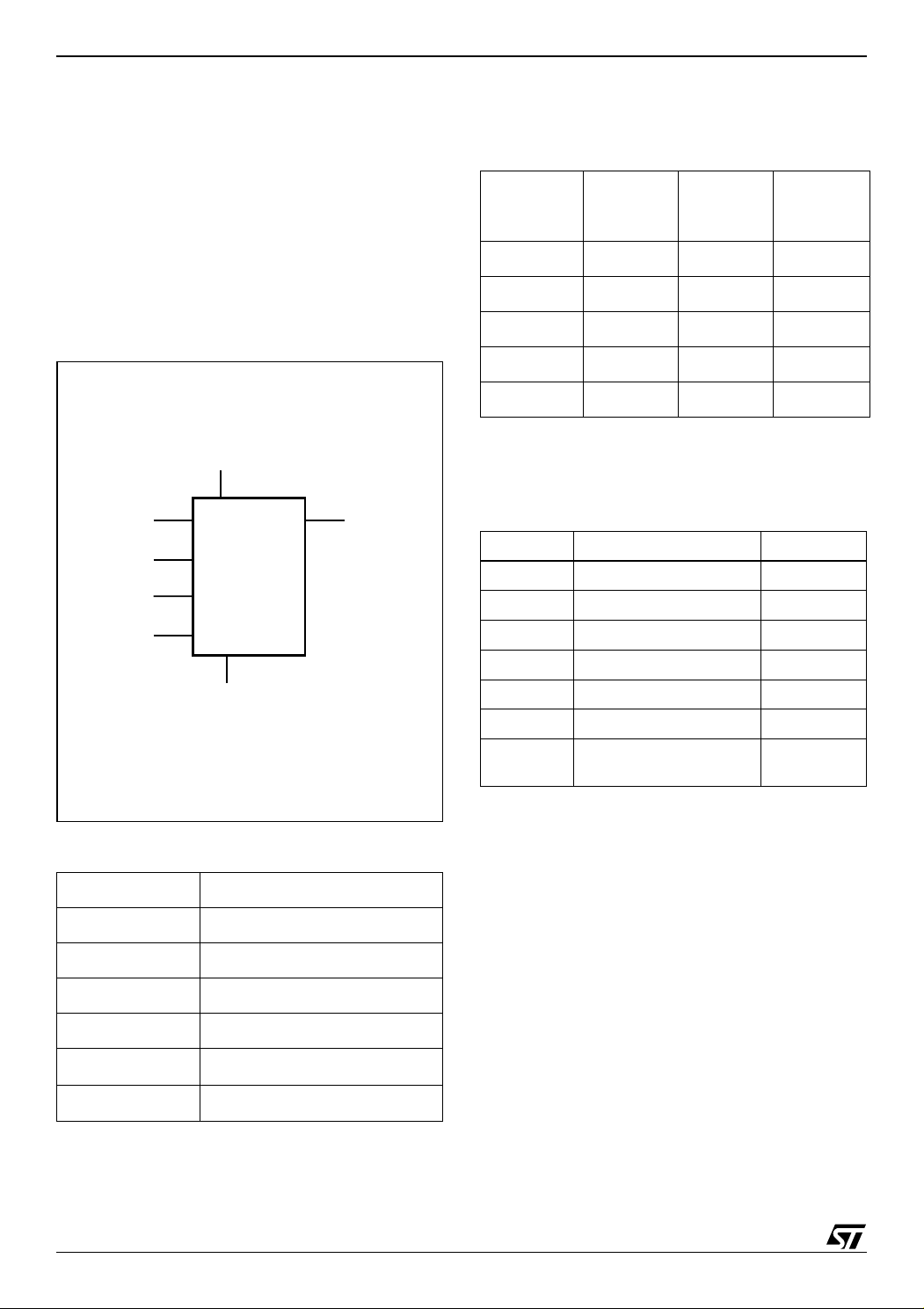
Figure 2. Logic Diagram
D
C
S
ORG
V
CC
M93Cx6
V
SS
www.st.com
.
Q
AI01928
lect (ORG). The bit, byte and word sizes of the
memories are as shown in Table 3.
Table 3. Memory Size versus Organization
Device
M93C86 16384 2048 1024
M93C76 8192 1024 512
M93C66 4096 512 256
M93C56 2048 256 128
M93C46 1024 128 64
Number
of Bits
Number
of 8-bit
Bytes
Number
of 16-bit
Words
The M93Cx6 is access ed by a set of inst ruction s,
as summarized in Table 4 ., and in more detail in
Table 5. to Table 7.).
Table 4. Instruction Set for the M93Cx6
Instruction Description Data
READ Read Data from Memory Byte or Word
WRITE Write Data to Memory Byte or Word
EWEN Erase/Write Enable
EWDS Erase/Write Disable
ERASE Erase Byte or Word Byte or Word
ERAL Erase All Memory
WRAL
Write All Memory
with same Data
Table 2. Signal Names
S Chip Select Input
D Serial Data Input
Q Serial Data Output
C Serial Clock
ORG Organisation Select
V
CC
V
SS
Supply Voltage
Ground
The memory array organization may be divided
into either bytes (x8) or words (x16) which may be
selected by a sig nal applied on Or ganization Se-
4/31
A Read Data from Memory (READ) instruction
loads the address of the first byte or word to be
read in an internal address register. The data at
this address is then cloc ked out serially. The address register is automatically incremented after
the data is output and, if Chip S elect Input (S) is
held High, the M93Cx6 can output a sequential
stream of data bytes or words. In this way, the
memory can be read as a data stream fr om eight
to 16384 bits long (in the case of the M93C86), or
continuously (the address counter automatically
rolls over to 00h when the highest address is
reached).
Programming is inte rnally self- timed (the external
clock signal on Serial Clock (C) may be stopped or
left running after the start of a Write cycle) and
does not require an Erase cycle pr ior to the Write
instruction. The Write instruction writes 8 or 16 bits
at a time into one o f the byte or word lo cations of
the M93Cx6. After the start of the programming cycle, a Busy/Ready signal is available on Serial
M93C86, M93C76, M93C66, M93C56, M93C46
Data Output (Q) wh en Chip Select I nput (S) is driven High.
An internal Power-on Data Protection mechanism
in the M93Cx6 inhibits the device when the supply
is too low.
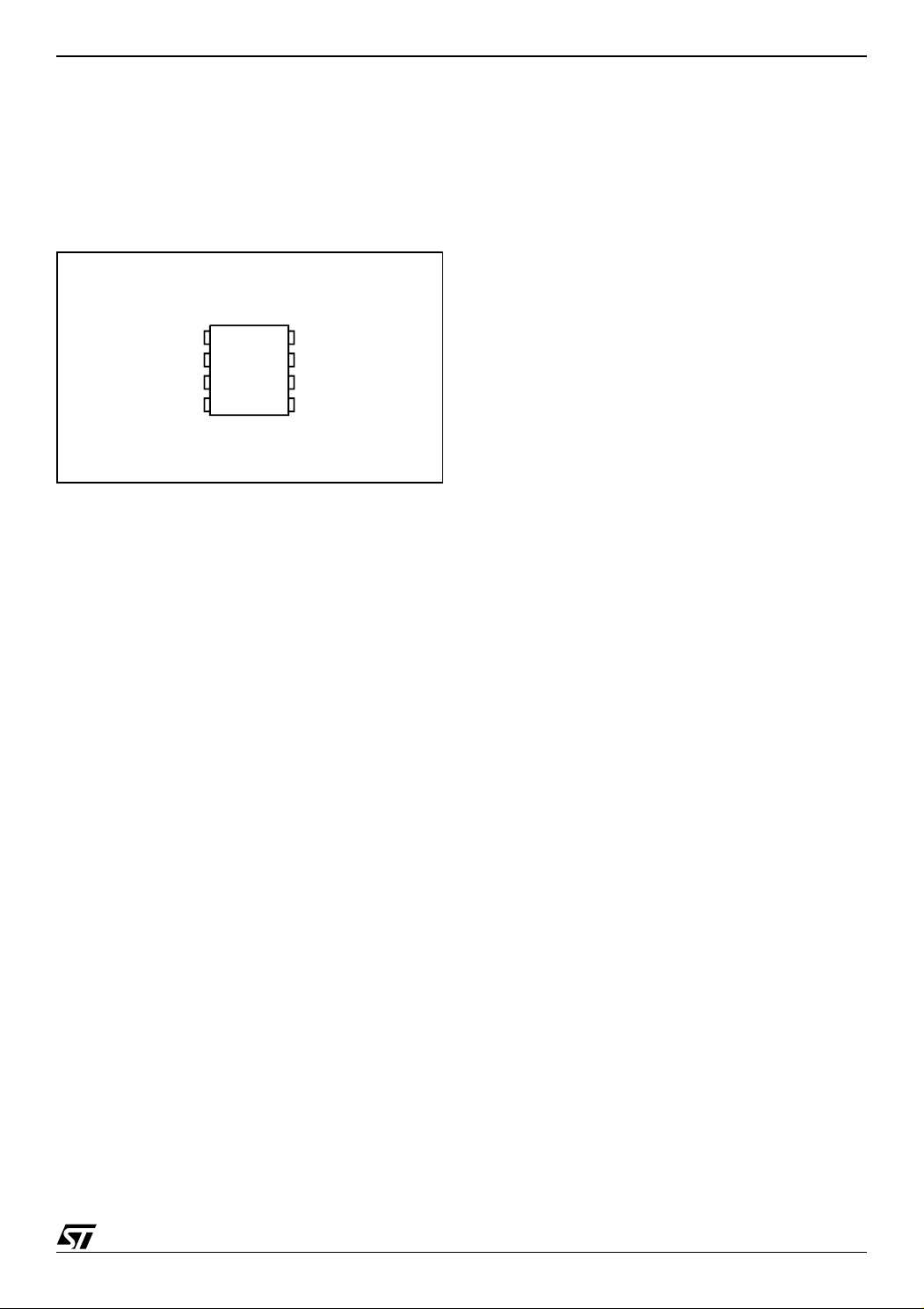
Figure 3. DIP, SO, TSSOP and MLP Connections (Top View)
M93Cx6
SV
1
2
D
3
Q
4
Note: 1. See PACKAGE MECHANICAL section for package di-
mensions, and how to identify pin-1.
2. DU = Don’t Use.
8
7
6
5
AI01929B
CC
DUC
ORG
V
SS
The DU (Don’t Use) pin does not contribute to the
normal operation of the dev ice. It is reserved for
use by STMicroelectronics during test sequences.
The pin may be left unconn ected or may be con nected to V
is recommended for the lowest stand-by pow-
V
SS
or VSS. Direct connection of DU to
CC
er consumption.
5/31

M93C86, M93C76, M93C66, M93C56, M93C46
MEMORY ORGANIZATION
The M93Cx6 memory is organized either as bytes
(x8) or as words (x16). If Organization Select
(ORG) is left unconnected (or connected to V
CC
the x16 organization is selected; w hen Organiza tion Select (ORG) i s connected to Ground (V
SS
is in stand-by mo de, Organization Select (ORG)
should be set either to V
power consumption. Any voltage between V
)
and VCC applied to Organization Select (ORG)
may increase the stand-by current.
)
the x8 organization is selected. When the M93Cx6
INTERNAL DEVICE RESET
In order to prevent inadvertent Write operations
during Power-up, a Power On Reset (POR) circuit
is included.
At Power-up and Power-down, the device must
not
be selected (that is, the Chip Sel ect Input (S)
must be driven Low) until the supply voltage
reaches the operating v oltage V
(as defined in
CC
Tables 9, 10 and 11).
During Power-up (phase during whic h V
er than V
min but increases continuously), the
CC
device will not respond to any instruction until V
is low-
CC
CC
has reached the Power On Rese t threshold voltage (this threshold is lower than the minimum V
CC
operating voltage defined in DC AND AC PARAM-
ETERS). Once V
old, the device is reset.
Prior to selecting the memory and issuing instruc-
tions to it, a valid and stab le V
applied. This voltage must remain stable and valid
until the end of the transmissi on of the instruc tion
and, for a Write instruction, until the completion of
the internal write cycle (t
During Power-down (phase during which V
creases continuously), as soon as V
the normal operating voltag e below the Po wer On
Reset threshold voltage, the device stops responding to any instruction sent to it.
ACTIVE POWER AND STANDBY POWER MODES
or VCC for minimum
SS
has passed the POR thresh -
CC
voltage must be
CC
).
W
drops from
CC
CC
SS
de-
When Chip Select (S) is High, the device is selected and in the Active Power mode. It consumes
I
, as specified in Tables 15, 16, 17, 18 and 19.
CC
When Chip Select (S) is Low, the device is deselected.
If no Erase/Write cycle is i n progress when Chip
Select goes Low, the device enters the Sta ndby
Power mode, and the power consumption drops to
I
.
CC1
For the M93Cx6 devices (5V range) the POR
threshold voltage is ar ound 3V. For the M93Cx6W (3V range) and M93Cx6-R (2V range) the POR
threshold voltage is around 1.5V.
6/31

INSTRUCTIONS
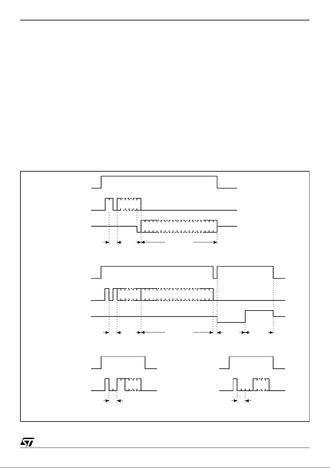
M93C86, M93C76, M93C66, M93C56, M93C46
The instruction set of the M93Cx6 devices contains seven instruc tions, as summar ized in Table
5. to Table 7.. Each instruction consists of the fol-
lowing parts, as shown in Figure 4.:
■ Each instruction is preceded by a rising edge
on Chip Select Input (S) with Serial Clock (C)
being held Low.
■ A start bit, which is the first ‘1’ read on Serial
Data Input (D) during the rising edge of Serial
Clock (C).
■ Two op-code bits, read on Serial Data Input
(D) during the rising edge of Serial Clock (C).
(Some instructions also use the first two bits of
the address to define the op-code).
■ The address bits of the byte or word that is to
be accessed. For the M93C46, the address is
made up of 6 bits for the x16 organization or 7
bits for the x8 organization (see Table 5.). For
the M93C56 and M93C66, the address is
made up of 8 bits for the x16 organization or 9
bits for the x8 organization (see Table 6.). For
the M93C76 and M93C86, the address is
made up of 10 bits for the x16 organization or
11 bits for the x8 organization (see Table 7.).
The M93Cx6 devices are fabricated in CMOS
technology and are th erefore able to run as slow
as 0 Hz (static input signals) or as fast as the maximum ratings specified in Table 20. to Table 23..
Table 5. Instruction Set for the M93C46
x8 Origination (ORG = 0) x16 Origination (ORG = 1)
Instruc
tion
READ
WRITE
EWEN Erase/Write Enable 1 00 11X XXXX 10 11 XXXX 9
EWDS Erase/Write Disable 1 00 00X XXXX 10 00 XXXX 9
ERASE Erase Byte or Word 1 11 A6-A0 10 A5-A0 9
ERAL Erase All Memory 1 00 10X XXXX 10 10 XXXX 9
WRAL
Note: 1. X = Don't Care bit.
Description
Read Data from
Memory
Write Data to
Memory
Write All Memory
with same Data
Start
Op-
bit
Code
1 10 A6-A0 Q7-Q0 A5-A0 Q15-Q0
1 01 A6-A0 D7-D0 18 A5-A0 D15-D0 25
1 00 01X XXXX D7-D0 18 01 XXXX D15-D0 25
Address
(1)
Data
Required
Clock
Cycles
Address
(1)
Data
Required
Cycles
Clock
7/31

M93C86, M93C76, M93C66, M93C56, M93C46
Table 6. Instruction Set for the M93C56 and M93C66
x8 Origination (ORG = 0) x16 Origination (ORG = 1)
Instruction Description
READ
WRITE
Read Data from
Memory
Write Data to
Memory
Start
EWEN Erase/Write Enable 1 00
EWDS Erase/Write Disable 1 00
ERASE Erase Byte or Word 1 11 A8-A0 12 A7-A0 11
ERAL Erase All Me mo ry 1 00
WRAL
Note: 1. X = Don't Care bit.
Write All Memory
with same Data
2. Address bit A8 is not decoded by the M93C56.
3. Address bit A7 is not decoded by the M93C56.
bit
Op-
Code
Address
(1,2)
Data
Required
Clock
Cycles
Address
(1,3)
Data
Required
Clock
Cycles
1 10 A8-A0 Q7-Q0 A7-A0 Q15-Q0
1 01 A8-A0 D7-D0 20 A7-A0 D15-D0 27
100
1 1XXX
XXXX
0 0XXX
XXXX
1 0XXX
XXXX
0 1XXX
XXXX
D7-D0 20 01XX XXXX D15-D0 27
12 11XX XXXX 11
12 00XX XXXX 11
12 10XX XXXX 11
Table 7. Instruction Set for the M93C76 and M93C86
x8 Origination (ORG = 0) x16 Origination (ORG = 1)
Instruction Description
READ
WRITE
Read Data from
Memory
Write Data to
Memory
Start
EWEN Erase/Write Enable 1 00
EWDS Erase/Write Disable 1 00
ERASE Erase Byte or Word 1 11 A10-A0 14 A9-A0 13
ERAL Erase All Me mo ry 1 00
WRAL
Note: 1. X = Don't Care bit.
Write All Memory
with same Data
2. Address bit A10 is not decoded by the M93C76.
3. Address bit A9 is not decoded by the M93C76.
bit
Op-
Code
Address
(1,2)
Data
Required
Clock
Cycles
Address
(1,3)
Data
Required
Clock
Cycles
1 10 A10-A0 Q7-Q0 A9-A0 Q15-Q0
1 01 A10-A0 D7-D0 22 A9-A0 D15-D0 29
100
11X XXXX
XXXX
00X XXXX
XXXX
10X XXXX
XXXX
01X XXXX
XXXX
14
14
14
D7-D0 22
11 XXXX
XXXX
00 XXXX
XXXX
10 XXXX
XXXX
01 XXXX
XXXX
D15-D0 29
13
13
13
8/31
M93C86, M93C76, M93C66, M93C56, M93C46
Read
The Read Data from Memory (READ) instruction
outputs data on Serial Data Output (Q). Wh en the
instruction is receive d, the op-code and address
are decoded, and the data from the memory is
transferred to an output shift register. A dummy 0
bit is output first, fol lowed by the 8-b it byte or 16bit word, with the most significant bi t first. Output
data changes are trigg ered by the rising edge of
Serial Clock (C). The M93Cx6 automatically increments the internal address register and clocks out
the next byte (or word) a s long as th e Chi p Se le ct
Input (S) is held High. In this case, the dummy 0 bit
is
not
output between bytes (or words) and a con-
tinuous stream of data can be read.
Figure 4. READ, WRITE, EWEN, EWDS Sequences
READ
S
D
1 1 0 An A0
Erase/Write Enable and Disable
The Erase/Write Enable (EWEN) instruction enables the future execution of erase or write instructions, and the Erase/Write Disable (EWDS)
instruction disables it. When power is first applied,
the M93Cx6 initializes itself so that erase and write
instructions are disabled. After an Erase/Write Enable (EWEN) instruction has been executed, erasing and writing remains enabled until an Erase/
Write Disable (EWDS) instruction is executed, or
until V
falls below the po wer -on r eset thr es ho ld
CC
voltage. To protect the me mory co ntents fr om accidental corruption, it is advisable to issue the
Erase/Write Disab le (EWDS) instruction after every write cycle. The Read Data from Memory
(READ) instruction is not affected by the Erase/
Write Enable (EWEN) or Erase/Write Disable
(EWDS) instructions.
Q
ADDR
OP
CODE
SWRITE
D
Q
SERASE
WRITE
ENABLE
D
Note: For the meanings of An, Xn, Qn and Dn, see Table 5., Table 6. and Table 7..
1 0An A0
ADDR
OP
CODE
1
0XnX0
101
OP
CODE
Qn Q0
DATA OUT
Dn D01
DATA IN
WRITE
DISABLE
CHECK
STATUS
BUSY READY
SERASE
1 0XnX0D
0 00
OP
CODE
AI00878C
9/31

M93C86, M93C76, M93C66, M93C56, M93C46
Erase
The Erase Byte or Word (ERASE) instruction sets
the bits of the addressed memory byte (or word) to
1. Once the address has b een corr ectly dec oded,
the falling edge of the Chi p Select Inpu t (S) st arts
the self-timed Era se cycle. Th e completion of the
cycle can be detected by monitoring the Ready/
Busy
line, as described in the READY/BUSY STA-
TUS section.
Write
For the Write Data to Memory (WRITE) instruction,
8 or 16 data bits follow th e op-code and addres s
bits. These form the byte or word that is to be written. As with the other bits, Seria l Data Inpu t (D ) is
sampled on the rising edge of Serial Clock (C).
Figure 5. ERASE, ERAL Sequences
SERASE
1 1D
1
An A0
After the last data bit has been sa mpl ed,
the Chip
Select Input (S) must be taken Low before the next
rising edge of Serial Clock (C).
If Chip Select Input
(S) is brought Low before or after this specific time
frame, the self-timed programming cycle will not
be started, and the addressed l ocation will not be
programmed. The completi on of the cycle ca n be
detected by monitoring the Ready/Busy
line, as
described later in this document.
Once the Write cyc le has been star ted, it is int er-
nally self-timed (the external clock signal on Serial
Clock (C) may be stopped o r left r un nin g aft er the
start of a Write cycle). The cycle is automatically
preceded by an Eras e cycle, so it is un necessar y
to execute an explicit erase instruction before a
Write Data to Memory (WRITE) instruction.
CHECK
STATUS
Q
ADDR
OP
CODE
ALL
Note: For the meanings of An and Xn, please see Ta ble 5., Table 6. and Table 7..
SERASE
1 0D
1
0 0
Xn X0
Q
ADDR
OP
CODE
BUSY READY
CHECK
STATUS
BUSY READY
AI00879B
10/31
 Loading...