

Page 1
16Kbit, 8Kbit, 4Kbit, 2Kbit and 1Kbit (8-bit or 16-bit wide)
FEATURES SUMMARY
M93C86, M93C76, M93C66
M93C56, M93C46
MICROWIRE® Serial Access EEPROM
■ Industry Standard MICROWIRE Bus
■ Single Supply Voltage:
– 4.5 to 5.5V for M93Cx6
– 2.5 to 5.5V for M93Cx6-W
– 1.8 to 5.5V for M93Cx6-R
■ Dual Organization: by Word (x16) or Byte (x8)
■ Programming Instructions that work on: Byte,
Word or Entire Memory
■ Self-timed Programming Cycle with Auto-
Erase: 5ms
■ Ready/Busy Signal During Programming
■ 2MHz Clock Rate
■ Sequential Read Operation
■ Enhanced ESD/Latch-Up Behavior
■ More than 1 Million Erase/Write Cycles
■ More than 40 Year Data Retention
■ Packages
– ECOPACK® (RoHS compliant)
Table 1. Product List
Reference
M93C86
M93C76
M93C66
Part
Number
M93C86
M93C86-W M93C56-W
M93C86-R M93C56-R
M93C76
M93C76-W M93C46-W
M93C76-R M93C46-R
M93C66
M93C66-W
M93C66-R
Reference
M93C56
M93C46
Part
Number
M93C56
M93C46
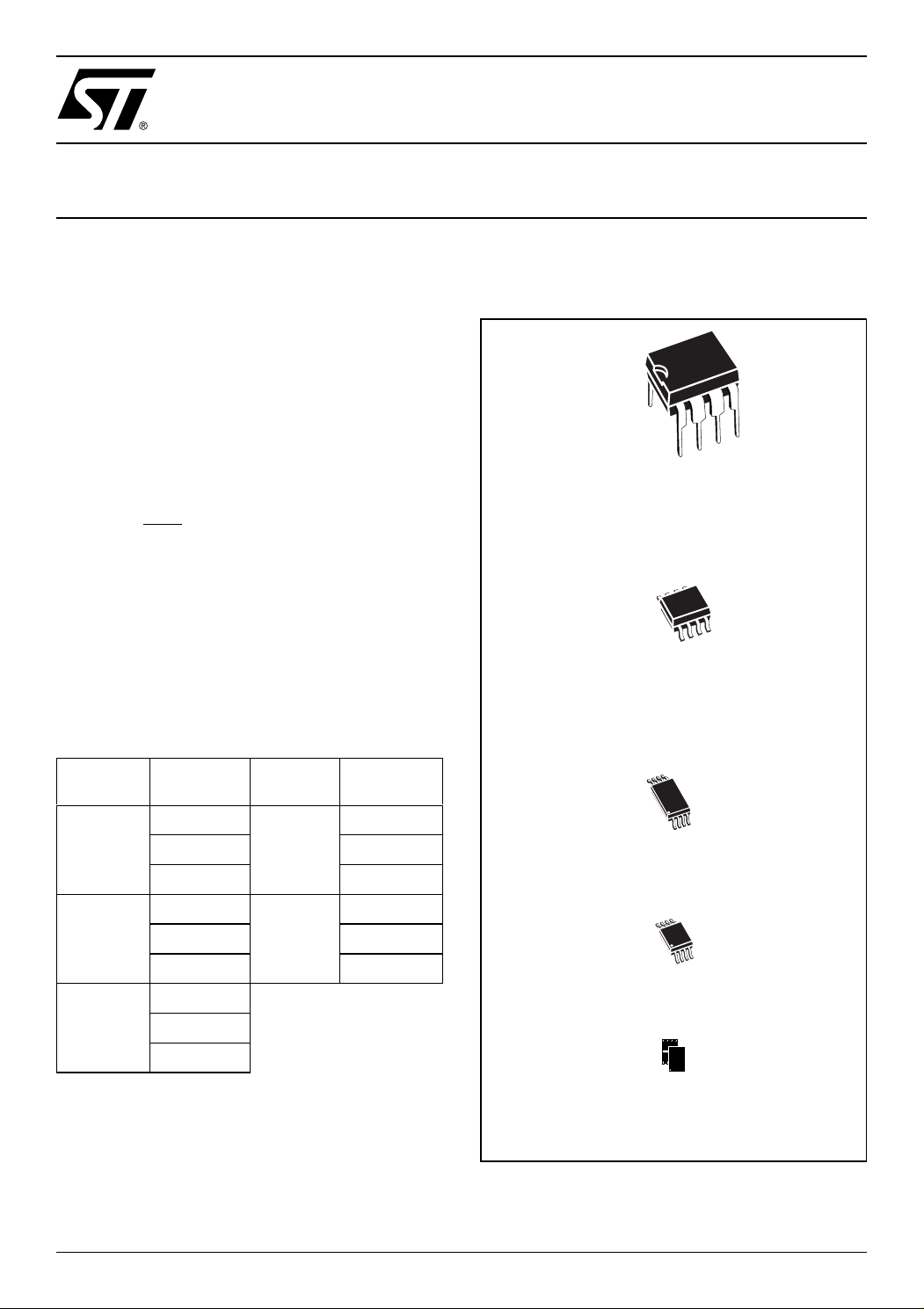
Figure 1. Packages
8
1
PDIP8 (BN)
8
1
SO8 (MN)
150 mil width
TSSOP8 (DW)
169 mil width
TSSOP8 (DS)
3x3mm² body size (MSOP)
UFDFPN8 (MB)
2x3mm² (MLP)
1/31October 2005
Page 2

M93C86, M93C76, M93C66, M93C56, M93C46
TABLE OF CONTENTS
FEATURES SUMMARY . . . . . . . . . . . . . . . . . . . . . . . . . . . . . . . . . . . . . . . . . . . . . . . . . . . . . . . . . . . . . 1
Table 1. Product List . . . . . . . . . . . . . . . . . . . . . . . . . . . . . . . . . . . . . . . . . . . . . . . . . . . . . . . . . . . . 1
Figure 1. Packages. . . . . . . . . . . . . . . . . . . . . . . . . . . . . . . . . . . . . . . . . . . . . . . . . . . . . . . . . . . . . . 1
Figure 2. Logic Diagram . . . . . . . . . . . . . . . . . . . . . . . . . . . . . . . . . . . . . . . . . . . . . . . . . . . . . . . . . . 4
Table 2. Signal Names . . . . . . . . . . . . . . . . . . . . . . . . . . . . . . . . . . . . . . . . . . . . . . . . . . . . . . . . . . 4
Table 3. Memory Size versus Organization. . . . . . . . . . . . . . . . . . . . . . . . . . . . . . . . . . . . . . . . . . . 4
Table 4. Instruction Set for the M93Cx6 . . . . . . . . . . . . . . . . . . . . . . . . . . . . . . . . . . . . . . . . . . . . .4
Figure 3. DIP, SO, TSSOP and MLP Connections (Top View). . . . . . . . . . . . . . . . . . . . . . . . . . . . . 5
MEMORY ORGANIZATION . . . . . . . . . . . . . . . . . . . . . . . . . . . . . . . . . . . . . . . . . . . . . . . . . . . . . . . . . . 6
INTERNAL DEVICE RESET . . . . . . . . . . . . . . . . . . . . . . . . . . . . . . . . . . . . . . . . . . . . . . . . . . . . . . . . . . 6
ACTIVE POWER AND STANDBY POWER MODES . . . . . . . . . . . . . . . . . . . . . . . . . . . . . . . . . . . . . . . 6
INSTRUCTIONS . . . . . . . . . . . . . . . . . . . . . . . . . . . . . . . . . . . . . . . . . . . . . . . . . . . . . . . . . . . . . . . . . . . 7
Table 5. Instruction Set for the M93C46 . . . . . . . . . . . . . . . . . . . . . . . . . . . . . . . . . . . . . . . . . . . . .7
Table 6. Instruction Set for the M93C56 and M93C66 . . . . . . . . . . . . . . . . . . . . . . . . . . . . . . . . . . 8
Table 7. Instruction Set for the M93C76 and M93C86 . . . . . . . . . . . . . . . . . . . . . . . . . . . . . . . . . . 8
Read . . . . . . . . . . . . . . . . . . . . . . . . . . . . . . . . . . . . . . . . . . . . . . . . . . . . . . . . . . . . . . . . . . . . . . . . . 9
Erase/Write Enable and Disable. . . . . . . . . . . . . . . . . . . . . . . . . . . . . . . . . . . . . . . . . . . . . . . . . . . 9
Figure 4. READ, WRITE, EWEN, EWDS Sequences. . . . . . . . . . . . . . . . . . . . . . . . . . . . . . . . . . . . 9
Erase. . . . . . . . . . . . . . . . . . . . . . . . . . . . . . . . . . . . . . . . . . . . . . . . . . . . . . . . . . . . . . . . . . . . . . . . 10
Write . . . . . . . . . . . . . . . . . . . . . . . . . . . . . . . . . . . . . . . . . . . . . . . . . . . . . . . . . . . . . . . . . . . . . . . . 10
Figure 5. ERASE, ERAL Sequences . . . . . . . . . . . . . . . . . . . . . . . . . . . . . . . . . . . . . . . . . . . . . . . 10
Erase All . . . . . . . . . . . . . . . . . . . . . . . . . . . . . . . . . . . . . . . . . . . . . . . . . . . . . . . . . . . . . . . . . . . . . 11
Write All . . . . . . . . . . . . . . . . . . . . . . . . . . . . . . . . . . . . . . . . . . . . . . . . . . . . . . . . . . . . . . . . . . . . . 11
Figure 6. WRAL Sequence . . . . . . . . . . . . . . . . . . . . . . . . . . . . . . . . . . . . . . . . . . . . . . . . . . . . . . . 11
READY/BUSY STATUS . . . . . . . . . . . . . . . . . . . . . . . . . . . . . . . . . . . . . . . . . . . . . . . . . . . . . . . . . . . . 12
INITIAL DELIVERY STATE. . . . . . . . . . . . . . . . . . . . . . . . . . . . . . . . . . . . . . . . . . . . . . . . . . . . . . . . . . 12
COMMON I/O OPERATION . . . . . . . . . . . . . . . . . . . . . . . . . . . . . . . . . . . . . . . . . . . . . . . . . . . . . . . . . 12
CLOCK PULSE COUNTER . . . . . . . . . . . . . . . . . . . . . . . . . . . . . . . . . . . . . . . . . . . . . . . . . . . . . . . . . 12
Figure 7. Write Sequence with One Clock Glitch . . . . . . . . . . . . . . . . . . . . . . . . . . . . . . . . . . . . . . 12
MAXIMUM RATING. . . . . . . . . . . . . . . . . . . . . . . . . . . . . . . . . . . . . . . . . . . . . . . . . . . . . . . . . . . . . . . . 13
Table 8. Absolute Maximum Ratings. . . . . . . . . . . . . . . . . . . . . . . . . . . . . . . . . . . . . . . . . . . . . . . 13
DC AND AC PARAMETERS. . . . . . . . . . . . . . . . . . . . . . . . . . . . . . . . . . . . . . . . . . . . . . . . . . . . . . . . . 14
Table 9. Operating Conditions (M93Cx6) . . . . . . . . . . . . . . . . . . . . . . . . . . . . . . . . . . . . . . . . . . . 14
Table 10. Operating Conditions (M93Cx6-W) . . . . . . . . . . . . . . . . . . . . . . . . . . . . . . . . . . . . . . . . . 14
Table 11. Operating Conditions (M93Cx6-R) . . . . . . . . . . . . . . . . . . . . . . . . . . . . . . . . . . . . . . . . . 14
2/31
Page 3

M93C86, M93C76, M93C66, M93C56, M93C46
Table 12. AC Measurement Conditions (M93Cx6) . . . . . . . . . . . . . . . . . . . . . . . . . . . . . . . . . . . . . 15
Table 13. AC Measurement Conditions (M93Cx6-W and M93Cx6-R) . . . . . . . . . . . . . . . . . . . . . . 15
Figure 8. AC Testing Input Output Waveforms. . . . . . . . . . . . . . . . . . . . . . . . . . . . . . . . . . . . . . . . 15
Table 14. Capacitance. . . . . . . . . . . . . . . . . . . . . . . . . . . . . . . . . . . . . . . . . . . . . . . . . . . . . . . . . . . 15
Table 15. DC Characteristics (M93Cx6, Device Grade 6). . . . . . . . . . . . . . . . . . . . . . . . . . . . . . . . 16
Table 16. DC Characteristics (M93Cx6, Device Grade 7 or 3) . . . . . . . . . . . . . . . . . . . . . . . . . . . . 16
Table 17. DC Characteristics (M93Cx6-W, Device Grade 6) . . . . . . . . . . . . . . . . . . . . . . . . . . . . . 17
Table 18. DC Characteristics (M93Cx6-W, Device Grade 7 or 3) . . . . . . . . . . . . . . . . . . . . . . . . . . 18
Table 19. DC Characteristics (M93Cx6-R) . . . . . . . . . . . . . . . . . . . . . . . . . . . . . . . . . . . . . . . . . . . 18
Table 20. AC Characteristics (M93Cx6, Device Grade 6, 7 or 3) . . . . . . . . . . . . . . . . . . . . . . . . . . 19
Table 21. AC Characteristics (M93Cx6-W, Device Grade 6). . . . . . . . . . . . . . . . . . . . . . . . . . . . . . 20
Table 22. AC Characteristics (M93Cx6-W, Device Grade 7 or 3) . . . . . . . . . . . . . . . . . . . . . . . . . . 21
Table 23. AC Characteristics (M93Cx6-R) . . . . . . . . . . . . . . . . . . . . . . . . . . . . . . . . . . . . . . . . . . . 22
Figure 9. Synchronous Timing (Start and Op-Code Input) . . . . . . . . . . . . . . . . . . . . . . . . . . . . . . . 23
Figure 10.Synchronous Timing (Read or Write) . . . . . . . . . . . . . . . . . . . . . . . . . . . . . . . . . . . . . . . 23
Figure 11.Synchronous Timing (Read or Write) . . . . . . . . . . . . . . . . . . . . . . . . . . . . . . . . . . . . . . . 23
PACKAGE MECHANICAL . . . . . . . . . . . . . . . . . . . . . . . . . . . . . . . . . . . . . . . . . . . . . . . . . . . . . . . . . . 24
Figure 12.PDIP8 – 8 pin Plastic DIP, 0.25mm lead frame, Package Outline . . . . . . . . . . . . . . . . . 24
Table 24. PDIP8 – 8 pin Plastic DIP, 0.25mm lead frame, Package Mechanical Data . . . . . . . . . . 24
Figure 13.SO8 narrow – 8 lead Plastic Small Outline, 150 mils body width, Package Outline . . . . 25
Table 25. SO8 narrow – 8 lead Plastic Small Outline, 150 mils body width, Package Data . . . . . . 25
Figure 14.UFDFPN8 (MLP8) 8-lead Ultra thin Fine pitch Dual Flat Package No lead 2x3mm²,
Outline . . . . . . . . . . . . . . . . . . . . . . . . . . . . . . . . . . . . . . . . . . . . . . . . . . . . . . . . . . . . . . . 26
Table 26. UFDFPN8 (MLP8) 8-lead Ultra thin Fine pitch Dual Flat Package No lead 2x3mm²,
Data. . . . . . . . . . . . . . . . . . . . . . . . . . . . . . . . . . . . . . . . . . . . . . . . . . . . . . . . . . . . . . . . . 26
Figure 15.TSSOP8 3x3mm² – 8 lead Thin Shrink Small Outline, 3x3mm² body size, Package
Outline . . . . . . . . . . . . . . . . . . . . . . . . . . . . . . . . . . . . . . . . . . . . . . . . . . . . . . . . . . . . . . . 27
Table 27. TSSOP8 3x3mm² – 8 lead Thin Shrink Small Outline, 3x3mm² body size,
Mechanical Data . . . . . . . . . . . . . . . . . . . . . . . . . . . . . . . . . . . . . . . . . . . . . . . . . . . . . . . 27
Figure 16.TSSOP8 – 8 lead Thin Shrink Small Outline, Package Outline . . . . . . . . . . . . . . . . . . . 28
Table 28. TSSOP8 – 8 lead Thin Shrink Small Outline, Package Mechanical Data . . . . . . . . . . . . 28
PART NUMBERING . . . . . . . . . . . . . . . . . . . . . . . . . . . . . . . . . . . . . . . . . . . . . . . . . . . . . . . . . . . . . . . 29
Table 29. Ordering Information Scheme . . . . . . . . . . . . . . . . . . . . . . . . . . . . . . . . . . . . . . . . . . . . . 29
REVISION HISTORY. . . . . . . . . . . . . . . . . . . . . . . . . . . . . . . . . . . . . . . . . . . . . . . . . . . . . . . . . . . . . . . 31
Table 30. Document Revision History . . . . . . . . . . . . . . . . . . . . . . . . . . . . . . . . . . . . . . . . . . . . . . . 31
3/31
Page 4
M93C86, M93C76, M93C66, M93C56, M93C46
SUMMARY DESCRIPTION
These electrically erasa ble pr ogram mable memory (EEPROM) devices are accessed through a Serial Data Input (D) and Serial Data Output (Q)
using the MICROWIRE bus protocol.
In order to meet environme ntal requirements, ST
offers these devices in ECOPACK® packages.
ECOPACK® packages are Lea d-free and RoHS
compliant.
ECOPACK is an ST trademark. ECOPACK specifications are available at:
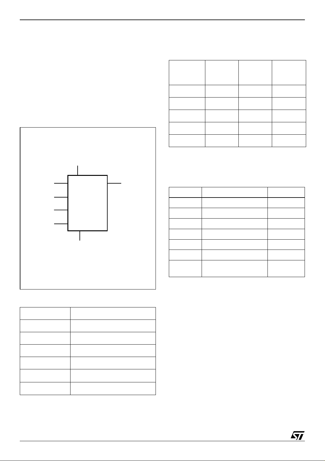
Figure 2. Logic Diagram
D
C
S
ORG
V
CC
M93Cx6
V
SS
www.st.com
.
Q
AI01928
lect (ORG). The bit, byte and word sizes of the
memories are as shown in Table 3.
Table 3. Memory Size versus Organization
Device
M93C86 16384 2048 1024
M93C76 8192 1024 512
M93C66 4096 512 256
M93C56 2048 256 128
M93C46 1024 128 64
Number
of Bits
Number
of 8-bit
Bytes
Number
of 16-bit
Words
The M93Cx6 is access ed by a set of inst ruction s,
as summarized in Table 4 ., and in more detail in
Table 5. to Table 7.).
Table 4. Instruction Set for the M93Cx6
Instruction Description Data
READ Read Data from Memory Byte or Word
WRITE Write Data to Memory Byte or Word
EWEN Erase/Write Enable
EWDS Erase/Write Disable
ERASE Erase Byte or Word Byte or Word
ERAL Erase All Memory
WRAL
Write All Memory
with same Data
Table 2. Signal Names
S Chip Select Input
D Serial Data Input
Q Serial Data Output
C Serial Clock
ORG Organisation Select
V
CC
V
SS
Supply Voltage
Ground
The memory array organization may be divided
into either bytes (x8) or words (x16) which may be
selected by a sig nal applied on Or ganization Se-
4/31
A Read Data from Memory (READ) instruction
loads the address of the first byte or word to be
read in an internal address register. The data at
this address is then cloc ked out serially. The address register is automatically incremented after
the data is output and, if Chip S elect Input (S) is
held High, the M93Cx6 can output a sequential
stream of data bytes or words. In this way, the
memory can be read as a data stream fr om eight
to 16384 bits long (in the case of the M93C86), or
continuously (the address counter automatically
rolls over to 00h when the highest address is
reached).
Programming is inte rnally self- timed (the external
clock signal on Serial Clock (C) may be stopped or
left running after the start of a Write cycle) and
does not require an Erase cycle pr ior to the Write
instruction. The Write instruction writes 8 or 16 bits
at a time into one o f the byte or word lo cations of
the M93Cx6. After the start of the programming cycle, a Busy/Ready signal is available on Serial
Page 5
M93C86, M93C76, M93C66, M93C56, M93C46
Data Output (Q) wh en Chip Select I nput (S) is driven High.
An internal Power-on Data Protection mechanism
in the M93Cx6 inhibits the device when the supply
is too low.
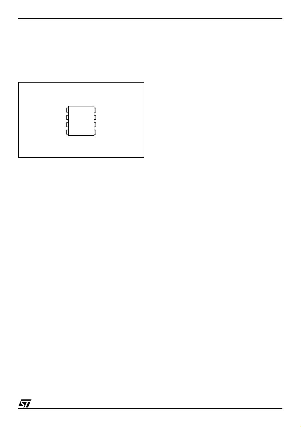
Figure 3. DIP, SO, TSSOP and MLP Connections (Top View)
M93Cx6
SV
1
2
D
3
Q
4
Note: 1. See PACKAGE MECHANICAL section for package di-
mensions, and how to identify pin-1.
2. DU = Don’t Use.
8
7
6
5
AI01929B
CC
DUC
ORG
V
SS
The DU (Don’t Use) pin does not contribute to the
normal operation of the dev ice. It is reserved for
use by STMicroelectronics during test sequences.
The pin may be left unconn ected or may be con nected to V
is recommended for the lowest stand-by pow-
V
SS
or VSS. Direct connection of DU to
CC
er consumption.
5/31
Page 6

M93C86, M93C76, M93C66, M93C56, M93C46
MEMORY ORGANIZATION
The M93Cx6 memory is organized either as bytes
(x8) or as words (x16). If Organization Select
(ORG) is left unconnected (or connected to V
CC
the x16 organization is selected; w hen Organiza tion Select (ORG) i s connected to Ground (V
SS
is in stand-by mo de, Organization Select (ORG)
should be set either to V
power consumption. Any voltage between V
)
and VCC applied to Organization Select (ORG)
may increase the stand-by current.
)
the x8 organization is selected. When the M93Cx6
INTERNAL DEVICE RESET
In order to prevent inadvertent Write operations
during Power-up, a Power On Reset (POR) circuit
is included.
At Power-up and Power-down, the device must
not
be selected (that is, the Chip Sel ect Input (S)
must be driven Low) until the supply voltage
reaches the operating v oltage V
(as defined in
CC
Tables 9, 10 and 11).
During Power-up (phase during whic h V
er than V
min but increases continuously), the
CC
device will not respond to any instruction until V
is low-
CC
CC
has reached the Power On Rese t threshold voltage (this threshold is lower than the minimum V
CC
operating voltage defined in DC AND AC PARAM-
ETERS). Once V
old, the device is reset.
Prior to selecting the memory and issuing instruc-
tions to it, a valid and stab le V
applied. This voltage must remain stable and valid
until the end of the transmissi on of the instruc tion
and, for a Write instruction, until the completion of
the internal write cycle (t
During Power-down (phase during which V
creases continuously), as soon as V
the normal operating voltag e below the Po wer On
Reset threshold voltage, the device stops responding to any instruction sent to it.
ACTIVE POWER AND STANDBY POWER MODES
or VCC for minimum
SS
has passed the POR thresh -
CC
voltage must be
CC
).
W
drops from
CC
CC
SS
de-
When Chip Select (S) is High, the device is selected and in the Active Power mode. It consumes
I
, as specified in Tables 15, 16, 17, 18 and 19.
CC
When Chip Select (S) is Low, the device is deselected.
If no Erase/Write cycle is i n progress when Chip
Select goes Low, the device enters the Sta ndby
Power mode, and the power consumption drops to
I
.
CC1
For the M93Cx6 devices (5V range) the POR
threshold voltage is ar ound 3V. For the M93Cx6W (3V range) and M93Cx6-R (2V range) the POR
threshold voltage is around 1.5V.
6/31
Page 7

INSTRUCTIONS
M93C86, M93C76, M93C66, M93C56, M93C46
The instruction set of the M93Cx6 devices contains seven instruc tions, as summar ized in Table
5. to Table 7.. Each instruction consists of the fol-
lowing parts, as shown in Figure 4.:
■ Each instruction is preceded by a rising edge
on Chip Select Input (S) with Serial Clock (C)
being held Low.
■ A start bit, which is the first ‘1’ read on Serial
Data Input (D) during the rising edge of Serial
Clock (C).
■ Two op-code bits, read on Serial Data Input
(D) during the rising edge of Serial Clock (C).
(Some instructions also use the first two bits of
the address to define the op-code).
■ The address bits of the byte or word that is to
be accessed. For the M93C46, the address is
made up of 6 bits for the x16 organization or 7
bits for the x8 organization (see Table 5.). For
the M93C56 and M93C66, the address is
made up of 8 bits for the x16 organization or 9
bits for the x8 organization (see Table 6.). For
the M93C76 and M93C86, the address is
made up of 10 bits for the x16 organization or
11 bits for the x8 organization (see Table 7.).
The M93Cx6 devices are fabricated in CMOS
technology and are th erefore able to run as slow
as 0 Hz (static input signals) or as fast as the maximum ratings specified in Table 20. to Table 23..
Table 5. Instruction Set for the M93C46
x8 Origination (ORG = 0) x16 Origination (ORG = 1)
Instruc
tion
READ
WRITE
EWEN Erase/Write Enable 1 00 11X XXXX 10 11 XXXX 9
EWDS Erase/Write Disable 1 00 00X XXXX 10 00 XXXX 9
ERASE Erase Byte or Word 1 11 A6-A0 10 A5-A0 9
ERAL Erase All Memory 1 00 10X XXXX 10 10 XXXX 9
WRAL
Note: 1. X = Don't Care bit.
Description
Read Data from
Memory
Write Data to
Memory
Write All Memory
with same Data
Start
Op-
bit
Code
1 10 A6-A0 Q7-Q0 A5-A0 Q15-Q0
1 01 A6-A0 D7-D0 18 A5-A0 D15-D0 25
1 00 01X XXXX D7-D0 18 01 XXXX D15-D0 25
Address
(1)
Data
Required
Clock
Cycles
Address
(1)
Data
Required
Cycles
Clock
7/31
Page 8

M93C86, M93C76, M93C66, M93C56, M93C46
Table 6. Instruction Set for the M93C56 and M93C66
x8 Origination (ORG = 0) x16 Origination (ORG = 1)
Instruction Description
READ
WRITE
Read Data from
Memory
Write Data to
Memory
Start
EWEN Erase/Write Enable 1 00
EWDS Erase/Write Disable 1 00
ERASE Erase Byte or Word 1 11 A8-A0 12 A7-A0 11
ERAL Erase All Me mo ry 1 00
WRAL
Note: 1. X = Don't Care bit.
Write All Memory
with same Data
2. Address bit A8 is not decoded by the M93C56.
3. Address bit A7 is not decoded by the M93C56.
bit
Op-
Code
Address
(1,2)
Data
Required
Clock
Cycles
Address
(1,3)
Data
Required
Clock
Cycles
1 10 A8-A0 Q7-Q0 A7-A0 Q15-Q0
1 01 A8-A0 D7-D0 20 A7-A0 D15-D0 27
100
1 1XXX
XXXX
0 0XXX
XXXX
1 0XXX
XXXX
0 1XXX
XXXX
D7-D0 20 01XX XXXX D15-D0 27
12 11XX XXXX 11
12 00XX XXXX 11
12 10XX XXXX 11
Table 7. Instruction Set for the M93C76 and M93C86
x8 Origination (ORG = 0) x16 Origination (ORG = 1)
Instruction Description
READ
WRITE
Read Data from
Memory
Write Data to
Memory
Start
EWEN Erase/Write Enable 1 00
EWDS Erase/Write Disable 1 00
ERASE Erase Byte or Word 1 11 A10-A0 14 A9-A0 13
ERAL Erase All Me mo ry 1 00
WRAL
Note: 1. X = Don't Care bit.
Write All Memory
with same Data
2. Address bit A10 is not decoded by the M93C76.
3. Address bit A9 is not decoded by the M93C76.
bit
Op-
Code
Address
(1,2)
Data
Required
Clock
Cycles
Address
(1,3)
Data
Required
Clock
Cycles
1 10 A10-A0 Q7-Q0 A9-A0 Q15-Q0
1 01 A10-A0 D7-D0 22 A9-A0 D15-D0 29
100
11X XXXX
XXXX
00X XXXX
XXXX
10X XXXX
XXXX
01X XXXX
XXXX
14
14
14
D7-D0 22
11 XXXX
XXXX
00 XXXX
XXXX
10 XXXX
XXXX
01 XXXX
XXXX
D15-D0 29
13
13
13
8/31
Page 9
M93C86, M93C76, M93C66, M93C56, M93C46
Read
The Read Data from Memory (READ) instruction
outputs data on Serial Data Output (Q). Wh en the
instruction is receive d, the op-code and address
are decoded, and the data from the memory is
transferred to an output shift register. A dummy 0
bit is output first, fol lowed by the 8-b it byte or 16bit word, with the most significant bi t first. Output
data changes are trigg ered by the rising edge of
Serial Clock (C). The M93Cx6 automatically increments the internal address register and clocks out
the next byte (or word) a s long as th e Chi p Se le ct
Input (S) is held High. In this case, the dummy 0 bit
is
not
output between bytes (or words) and a con-
tinuous stream of data can be read.
Figure 4. READ, WRITE, EWEN, EWDS Sequences
READ
S
D
1 1 0 An A0
Erase/Write Enable and Disable
The Erase/Write Enable (EWEN) instruction enables the future execution of erase or write instructions, and the Erase/Write Disable (EWDS)
instruction disables it. When power is first applied,
the M93Cx6 initializes itself so that erase and write
instructions are disabled. After an Erase/Write Enable (EWEN) instruction has been executed, erasing and writing remains enabled until an Erase/
Write Disable (EWDS) instruction is executed, or
until V
falls below the po wer -on r eset thr es ho ld
CC
voltage. To protect the me mory co ntents fr om accidental corruption, it is advisable to issue the
Erase/Write Disab le (EWDS) instruction after every write cycle. The Read Data from Memory
(READ) instruction is not affected by the Erase/
Write Enable (EWEN) or Erase/Write Disable
(EWDS) instructions.
Q
ADDR
OP
CODE
SWRITE
D
Q
SERASE
WRITE
ENABLE
D
Note: For the meanings of An, Xn, Qn and Dn, see Table 5., Table 6. and Table 7..
1 0An A0
ADDR
OP
CODE
1
0XnX0
101
OP
CODE
Qn Q0
DATA OUT
Dn D01
DATA IN
WRITE
DISABLE
CHECK
STATUS
BUSY READY
SERASE
1 0XnX0D
0 00
OP
CODE
AI00878C
9/31
Page 10

M93C86, M93C76, M93C66, M93C56, M93C46
Erase
The Erase Byte or Word (ERASE) instruction sets
the bits of the addressed memory byte (or word) to
1. Once the address has b een corr ectly dec oded,
the falling edge of the Chi p Select Inpu t (S) st arts
the self-timed Era se cycle. Th e completion of the
cycle can be detected by monitoring the Ready/
Busy
line, as described in the READY/BUSY STA-
TUS section.
Write
For the Write Data to Memory (WRITE) instruction,
8 or 16 data bits follow th e op-code and addres s
bits. These form the byte or word that is to be written. As with the other bits, Seria l Data Inpu t (D ) is
sampled on the rising edge of Serial Clock (C).
Figure 5. ERASE, ERAL Sequences
SERASE
1 1D
1
An A0
After the last data bit has been sa mpl ed,
the Chip
Select Input (S) must be taken Low before the next
rising edge of Serial Clock (C).
If Chip Select Input
(S) is brought Low before or after this specific time
frame, the self-timed programming cycle will not
be started, and the addressed l ocation will not be
programmed. The completi on of the cycle ca n be
detected by monitoring the Ready/Busy
line, as
described later in this document.
Once the Write cyc le has been star ted, it is int er-
nally self-timed (the external clock signal on Serial
Clock (C) may be stopped o r left r un nin g aft er the
start of a Write cycle). The cycle is automatically
preceded by an Eras e cycle, so it is un necessar y
to execute an explicit erase instruction before a
Write Data to Memory (WRITE) instruction.
CHECK
STATUS
Q
ADDR
OP
CODE
ALL
Note: For the meanings of An and Xn, please see Ta ble 5., Table 6. and Table 7..
SERASE
1 0D
1
0 0
Xn X0
Q
ADDR
OP
CODE
BUSY READY
CHECK
STATUS
BUSY READY
AI00879B
10/31
Page 11

M93C86, M93C76, M93C66, M93C56, M93C46
Erase All
The Erase All Memory (ERAL) instruction erases
the whole memory (al l memory bits a re set to 1).
The format of the instruction require s that a dummy address be provided. T he Erase cycle i s conducted in the same way as the Erase instruction
(ERASE). The completion of the cycle can be detected by monitoring the Rea dy/Busy
line, as de-
scribed in the READY/BUSY STATUS section.
Write All
As with the Erase All Memory (ERAL) instruction,
the format of the Write All Memory with same Data
(WRAL) instruction requires that a dummy address be provid ed. A s with the Write D ata to Me mory (WRITE) instruction, the format of the Write All
Memory with same Data (WRAL) instruction requires that an 8-bit data byte, or 16-bi t d ata wor d,
be provided. This value is written to all the addresses of the memory dev ice. The completio n of
the cycle can be detected by monitoring the
Ready/Busy
Figure 6. WRAL Sequence
ALL
Note: For the meanings of Xn and Dn, please see Table 5., Table 6. and Table 7..
SWRITE
D
Q
1
0 00 1 Xn X0
OP
CODE
ADDR
Dn D0
DATA IN
line, as described next.
CHECK
STATUS
BUSY READY
AI00880C
11/31
Page 12

M93C86, M93C76, M93C66, M93C56, M93C46
READY/BUSY STATUS
While the Write or E rase cycle is underway, for a
WRITE, ERASE, WRAL or ERAL instruction, the
Busy signal (Q=0) is returned whenever Chip Select Input (S) is driven High. (Please note, though,
that there is an initial delay, of t
, before this
SLSH
status information becomes available). In this
state, the M93Cx6 ignores any data on the bus.
INITIAL DELIVERY STATE
The device is delivered with all bits in the memory
array set to 1 (each byte contains FFh).
COMMON I/O OPERATION
Serial Data Output (Q) and Serial Data Input (D )
can be connected to geth er , thr ou gh a c urre nt l im iting resistor, to form a common, single-wire data
bus. Some precautions must be taken when operating the memory in t his way, m ostly to pre vent a
short circuit current from flowing when the last address bit (A0) clashes with the first data bit on Serial Data Output (Q). Please see the application
note
AN394
for details.
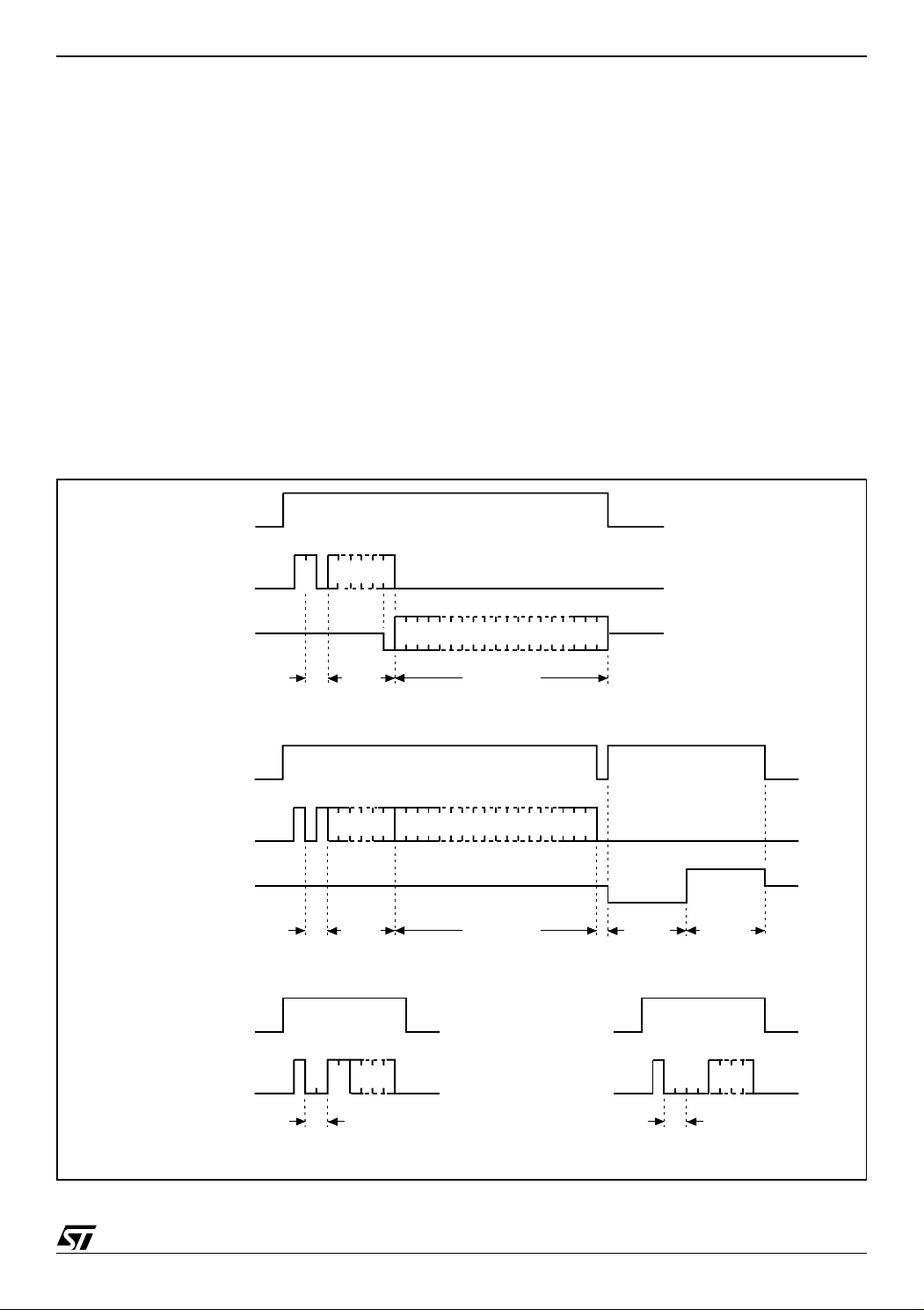
CLOCK PULSE COUNTER
In a noisy environment, the nu mber of pulses received on Serial Clock (C) may be greater than the
number delivered by the master (the microcontroller). This can lead to a misalignment of the instruction of one or more bits (as shown in Figure 7.) and
When the Write cycle is c ompleted, an d Chip Select Input (S) is driven High, the Ready signal
(Q=1) indicates that the M93Cx6 is rea dy to receive the next instructio n. Serial Data Output (Q)
remains set to 1 until the Ch ip Select Input (S) is
brought Low or until a new start bit is decoded.
may lead to the writing of erroneous data at an erroneous address.
To combat this proble m, the M93Cx6 has an onchip counter that counts the clock pulses from the
start bit until the falling edge of the Chip Select Input (S). If the number o f clock pulses rec eived is
not the number expected, the WRITE, ERASE,
ERAL or WRAL instruction is aborted, and the
contents of the memory are not modified.
The number of clock cycles expected for each instruction, and for each member of the M93Cx6
family, are summarized in Table 5. to Table 7.. For
example, a Write Data to Memory (WRITE) instruction on the M93C5 6 (or M9 3C66 ) ex pec ts 20
clock cycles (for the x8 organization) from the start
bit to the falling edge of Chip Select Input (S). That
is:
1 Start bit
+ 2 Op-code bits
+ 9 Address bits
+ 8 Data bits
Figure 7. Write Sequence with One C lock Glitch
S
C
D
An
START
WRITE
12/31
An-1
Glitch
An-2
ADDRESS AND DATA
ARE SHIFTED BY ONE BIT
D0"1""0"
AI01395
Page 13

MAXIMUM RATING
M93C86, M93C76, M93C66, M93C56, M93C46
Stressing the device above the ra ting l isted in the
Absolute Maximum Ratin gs table ma y cause permanent damage to the device. Thes e are stress
ratings only and operation of the device at these or
any other conditions abo ve those indica ted in the
plied. Exposu re to Abso lute Max imum Rati ng conditions for extended periods may affect device
reliability. Refer also to the STMicroelectronics
SURE Program and o ther relevant quality documents.
Operating sections of this specification is not im-
Table 8. Absolute Maximum Ratings
Symbol Parameter Min. Max. Unit
T
Ambient Operating Temperature –40 130 °C
A
T
T
LEAD
V
V
V
V
Note: 1. T
Storage Temperature –65 150 °C
STG
PDIP-Specific Lead Temperature during Soldering
Output range (Q = VOH or Hi-Z)
OUT
Input range –0.50
IN
Supply Voltage –0.50 6.5 V
CC
ESD
Electrostatic Discharge Voltage (Human Body model)
max must
LEAD
2. JEDEC Std JESD22-A114A (C1=100 pF, R1=1500 Ω, R2=500 Ω).
not
be applied for more than 10s.
(2)
–0.50
–4000 4000 V
V
260
CC
V
CC
(1)
+0.5
+1
°C
V
V
13/31
Page 14

M93C86, M93C76, M93C66, M93C56, M93C46
DC AND AC PARAMETERS
This section summ arizes the operati ng and measurement conditions , and the D C an d AC charac teristics of the device. The parameters in th e DC
and AC Characteristic tables that follow are derived from tests performed under the Measure-
ment Conditions summarized in the relevant
tables. Designers sho uld c heck tha t th e operating
conditions in thei r circui t match the measur ement
conditions when relying on the quoted parameters.
Table 9. Operating Conditions (M93Cx6)
Symbol Parameter Min. Max. Unit
V
CC
T
A
Supply Voltage 4.5 5.5 V
Ambient Operating Temperature (Device Grade 6) –40 85 °C
Ambient Operating Temperature (Device Grade 7) –40 105 °C
Ambient Operating Temperature (Device Grade 3) –40 125 °C
Table 10. Operating Conditions (M93Cx6-W)
Symbol Parameter Min. Max. Unit
V
CC
T
A
Supply Voltage 2.5 5.5 V
Ambient Operating Temperature (Device Grade 6) –40 85 °C
Ambient Operating Temperature (Device Grade 7) –40 105 °C
Ambient Operating Temperature (Device Grade 3) –40 125 °C
Table 11. Operating Conditions (M93Cx6-R)
Symbol Parameter Min. Max. Unit
V
CC
T
A
Supply Voltage 1.8 5.5 V
Ambient Operating Temperature (Device Grade 6) –40 85 °C
14/31
Page 15

M93C86, M93C76, M93C66, M93C56, M93C46
Table 12. AC Measurement Conditions (M93Cx6)
Symbol Parameter Min. Max. Unit
C
L
Load Capacitance 100 pF
Input Rise and Fall Times 50 ns
Input Pulse Voltages 0.4 V to 2.4 V V
Input Timing Reference Voltages 1.0 V and 2.0 V V
Output Timing Reference Voltages 0.8 V and 2.0 V V
Note: 1. Output Hi-Z is defined as the point where data out is no longer driven.
Table 13. AC Measurement Conditions (M93Cx6-W and M93Cx6-R)
Symbol Parameter Min. Max. Unit
C
L
Load Capacitance 100 pF
Input Rise and Fall Times 50 ns
0.2V
0.3V
0.3V
to 0.8V
CC
to 0.7V
CC
to 0.7V
CC
CC
CC
CC
Input Pulse Voltages
Input Timing Reference Voltages
Output Timing Reference Voltages
Note: 1. Output Hi-Z is defined as the point where data out is no longer driven.
Figure 8. AC Testing Input Output Waveforms
V
V
V
M93CXX
2V
1V
M93CXX-W & M93CXX-R
2.0V
0.8V
0.7V
0.3V
AI02553
CC
CC
0.8V
0.2V
2.4V
0.4V
INPUT OUTPUT
CC
CC
Table 14. Capacitance
Symbol Parameter Test Condition Min Max Unit
C
OUT
C
IN
Note: Sampled only, not 100% tested, at TA=25°C and a frequency of 1MHz.
Output
Capacitance
Input
Capacitance
V
OUT
V
IN
= 0V
= 0V
5pF
5pF
15/31
Page 16

M93C86, M93C76, M93C66, M93C56, M93C46
Table 15. DC Characteristics (M93Cx6, Device Grade 6)
Symbol Parameter Test Condition Min. Max. Unit
I
I
Input Leakage Current
LI
Output Leakage Current
LO
0V ≤ V
0V ≤ V
≤ V
IN
≤ VCC, Q in Hi-Z
OUT
CC
±2.5 µA
±2.5 µA
I
V
I
V
V
V
CC
CC1
Supply Current
Supply Current (Stand-by)
Input Low Voltage
IL
Input High Voltage
IH
Output Low Voltage
OL
Output High Voltage
OH
V
= 5V, S = VIH, f = 2 MHz, Q = open
CC
V
= 5V, S = VSS, C = VSS,
CC
ORG = V
V
CC
V
CC
V
= 5V, IOL = 2.1mA
CC
V
= 5V, IOH = –400µA
CC
or V
SS
CC
= 5V ± 10%
= 5V ± 10%
2 mA
15 µA
–0.45 0.8 V
2
VCC + 1
0.4 V
2.4 V
Table 16. DC Characteristics (M93Cx6, Device Grade 7 or 3)
Symbol Parameter Test Condition Min. Max. Unit
I
V
I
I
V
V
V
I
LI
LO
CC
CC1
OL
OH
Input Leakage Current
Output Leakage Current
Supply Current
Supply Current (Stand-by)
Input Low Voltage
IL
Input High Voltage
IH
Output Low Voltage
Output High Voltage
0V ≤ V
0V ≤ V
V
= 5V, S = VIH, f = 2 MHz, , Q = open
CC
V
= 5V, S = VSS, C = VSS,
CC
ORG = VSS or V
V
V
V
= 5V, IOL = 2.1mA
CC
V
= 5V, IOH = –400µA
CC
≤ V
IN
≤ VCC, Q in Hi-Z
OUT
= 5V ± 10%
CC
= 5V ± 10%
CC
CC
CC
±2.5 µA
±2.5 µA
2 mA
15 µA
–0.45 0.8 V
2
VCC + 1
0.4 V
2.4 V
V
V
16/31
Page 17

M93C86, M93C76, M93C66, M93C56, M93C46
Table 17. DC Characteristics (M93Cx6-W, Device Grade 6)
Symbol Parameter Test Condition Min. Max. Unit
I
V
I
I
V
V
V
I
LI
LO
CC
CC1
OL
OH
Input Leakage Current
Output Leakage Current
= 5V, S = VIH, f = 2 MHz, Q = open
V
Supply Current (CMOS
Inputs)
Supply Current (Stand-by)
Input Low Voltage (D, C, S) –0.45
IL
Input High Voltage (D, C, S)
IH
CC
= 2.5V, S = VIH, f = 2 MHz, Q = open
V
CC
V
Output Low Voltage (Q)
Output High Voltage (Q)
0V ≤ V
0V ≤ V
= 2.5V, S = VSS, C = VSS,
CC
ORG = V
V
= 5V, IOL = 2.1mA
CC
= 2.5V, IOL = 100µA
V
CC
= 5V, IOH = –400µA
V
CC
= 2.5V, IOH = –100µA VCC–0.2
V
CC
≤ V
IN
≤ VCC, Q in Hi-Z
OUT
or V
SS
CC
CC
±2.5 µA
±2.5 µA
2 mA
1 mA
5 µA
0.2 V
CC
0.7 V
CC
VCC + 1
0.4 V
0.2 V
2.4 V
V
V
V
17/31
Page 18

M93C86, M93C76, M93C66, M93C56, M93C46
Table 18. DC Characteristics (M93Cx6-W, Device Grade 7 or 3)
Symbol Parameter Test Condition
I
I
LO
I
CC
I
CC1
V
V
V
V
Note: 1. New product: identified by Process Identifica tion letter W or G or S.
Input Leakage Current
LI
Output Leakage Current
= 5V, S = VIH, f = 2 MHz, Q = open
V
Supply Current (CMOS
Inputs)
Supply Current (Stand-by)
Input Low Voltage (D, C, S) –0.45
IL
Input High Voltage (D, C, S)
IH
Output Low Voltage (Q)
OL
Output High Voltage (Q)
OH
CC
= 2.5V, S = VIH, f = 2 MHz, Q = open
V
CC
V
0V ≤ V
0V ≤ V
= 2.5V, S = VSS, C = VSS,
CC
ORG = VSS or V
V
= 5V, IOL = 2.1mA
CC
= 2.5V, IOL = 100µA
V
CC
= 5V, IOH = –400µA
V
CC
= 2.5V, IOH = –100µA VCC–0.2
V
CC
≤ V
IN
≤ VCC, Q in Hi-Z
OUT
CC
CC
Min.
(1)
Max.
(1)
Unit
±2.5 µA
±2.5 µA
2 mA
1 mA
5 µA
0.7 V
CC
0.2 V
VCC + 1
CC
V
V
0.4 V
0.2 V
2.4 V
V
Table 19. DC Characteristics (M93Cx6-R)
Symbol Parameter Test Condition
I
I
LO
I
CC
I
CC1
V
V
V
V
Note: 1. This product is under development. For more information, please contact your nearest ST sales of fice.
Input Leakage Current
LI
Output Leakage Current
= 5V, S = VIH, f = 2 MHz, Q = open
V
Supply Current (CMOS
Inputs)
Supply Current (Stand-by)
Input Low Voltage (D, C, S) –0.45
IL
Input High Voltage (D, C, S)
IH
Output Low Voltage (Q)
OL
Output High Voltage (Q)
OH
CC
= 1.8V, S = VIH, f = 1 MHz, Q = open
V
CC
V
0V ≤ V
0V ≤ V
= 1.8V, S = VSS, C = VSS,
CC
ORG = V
V
= 1.8V, IOL = 100µA
CC
V
= 1.8V, IOH = –100µA VCC–0.2
CC
≤ V
IN
≤ VCC, Q in Hi-Z
OUT
or V
SS
CC
CC
Min.
0.8 V
(1)
Max.
(1)
Unit
±2.5 µA
±2.5 µA
2 mA
1 mA
2 µA
CC
0.2 V
VCC + 1
CC
V
V
0.2 V
V
18/31
Page 19

M93C86, M93C76, M93C66, M93C56, M93C46
Table 20. AC Characteristics (M93Cx6, Device Grade 6, 7 or 3)
Test conditions specified in Table 12. and Table 9.
Symbol Alt. Parameter Min. Max. Unit
f
C
t
SLCH
t
SHCH
(2)
t
SLSH
(1)
t
CHCL
(1)
t
CLCH
t
DVCH
t
CHDX
t
CLSH
t
CLSL
t
SHQV
t
SLQZ
t
CHQL
t
CHQV
t
W
Note: 1. t
CHCL
2. Chip Select Input (S) must be brought Low for a minimum of t
f
SK
Clock Frequency D.C. 2 MHz
Chip Select Low to Clock High 50 ns
+ t
CLCH
t
CSS
t
CS
t
SKH
t
SKL
t
DIS
t
DIH
t
SKS
t
CSH
t
SV
t
DF
t
PD0
t
PD1
t
WP
≥ 1 / fC.
Chip Select Set-up Time
M93C46, M93C56, M93C66
Chip Select Set-up time
M93C76, M93C86
Chip Select Low to Chip Select High 200 ns
Clock High Time 200 ns
Clock Low Time 200 ns
Data In Set-up Time 50 ns
Data In Hold Time 50 ns
Clock Set-up Time (relative to S) 50 ns
Chip Select Hold Time 0 ns
Chip Select to Ready/Busy Status 200 ns
Chip Select Low to Output Hi-Z 100 ns
Delay to Output Low 200 ns
Delay to Output Valid 200 ns
Erase/Write Cycle time 5 ms
between consecutive instruction cycles.
SLSH
50 ns
50 ns
19/31
Page 20

M93C86, M93C76, M93C66, M93C56, M93C46
Table 21. AC Characteristics (M93Cx6-W, Device Grade 6)
Test conditions specified in Table 13. and Table 10.
Symbol Alt. Parameter Min. Max. Unit
f
C
t
SLCH
t
SHCH
(2)
t
SLSH
(1)
t
CHCL
(1)
t
CLCH
t
DVCH
t
CHDX
t
CLSH
t
CLSL
t
SHQV
t
SLQZ
t
CHQL
t
CHQV
t
W
Note: 1. t
CHCL
2. Chip Select Input (S) must be brought Low for a minimum of t
f
SK
Clock Frequency D.C. 2 MHz
Chip Select Low to Clock High 50 ns
+ t
CLCH
t
CSS
t
CS
t
SKH
t
SKL
t
DIS
t
DIH
t
SKS
t
CSH
t
SV
t
DF
t
PD0
t
PD1
t
WP
≥ 1 / fC.
Chip Select Set-up Time 50 ns
Chip Select Low to Chip Select High 200 ns
Clock High Time 200 ns
Clock Low Time 200 ns
Data In Set-up Time 50 ns
Data In Hold Time 50 ns
Clock Set-up Time (relative to S) 50 ns
Chip Select Hold Time 0 ns
Chip Select to Ready/Busy Status 200 ns
Chip Select Low to Output Hi-Z 100 ns
Delay to Output Low 200 ns
Delay to Output Valid 200 ns
Erase/Write Cycle time 5 ms
between consecutive instruction cycles.
SLSH
20/31
Page 21

M93C86, M93C76, M93C66, M93C56, M93C46
Table 22. AC Characteristics (M93Cx6-W, Device Grade 7 or 3)
Test conditions specified in Table 13. and Table 10.
Symbol Alt. Parameter Min. Max. Unit
f
C
t
SLCH
t
SHCH
(2)
t
SLSH
(1)
t
CHCL
(1)
t
CLCH
t
DVCH
t
CHDX
t
CLSH
t
CLSL
t
SHQV
t
SLQZ
t
CHQL
t
CHQV
t
W
Note: 1. t
CHCL
2. Chip Select Input (S) must be brought Low for a minimum of t
f
SK
Clock Frequency D.C. 2 MHz
Chip Select Low to Clock High 50 ns
+ t
CLCH
t
CSS
t
CS
t
SKH
t
SKL
t
DIS
t
DIH
t
SKS
t
CSH
t
SV
t
DF
t
PD0
t
PD1
t
WP
≥ 1 / fC.
Chip Select Set-up Time 50 ns
Chip Select Low to Chip Select High 200 ns
Clock High Time 200 ns
Clock Low Time 200 ns
Data In Set-up Time 50 ns
Data In Hold Time 50 ns
Clock Set-up Time (relative to S) 50 ns
Chip Select Hold Time 0 ns
Chip Select to Ready/Busy Status 200 ns
Chip Select Low to Output Hi-Z 100 ns
Delay to Output Low 200 ns
Delay to Output Valid 200 ns
Erase/Write Cycle time 5 ms
between consecutive instruction cycles.
SLSH
21/31
Page 22

M93C86, M93C76, M93C66, M93C56, M93C46
Table 23. AC Characteristics (M93Cx6-R)
Test conditions specified in Table 13. and Table 11.
Symbol Alt. Parameter
f
C
t
SLCH
t
SHCH
(2)
t
SLSH
(1)
t
CHCL
(1)
t
CLCH
t
DVCH
t
CHDX
t
CLSH
t
CLSL
t
SHQV
t
SLQZ
t
CHQL
t
CHQV
t
W
Note: 1. t
CHCL
2. Chip Select Input (S) must be brought Low for a minimum of t
3. This product is under development. For more information, please contact your nearest ST sales off i ce.
f
SK
Clock Frequency D.C. 1 MHz
Chip Select Low to Clock High 250 ns
+ t
CLCH
t
CSS
t
CS
t
SKH
t
SKL
t
DIS
t
DIH
t
SKS
t
CSH
t
SV
t
DF
t
PD0
t
PD1
t
WP
≥ 1 / fC.
Chip Select Set-up Time 50 ns
Chip Select Low to Chip Select High 250 ns
Clock High Time 250 ns
Clock Low Time 250 ns
Data In Set-up Time 100 n s
Data In Hold Time 100 n s
Clock Set-up Time (relative to S) 100 ns
Chip Select Hold Time 0 ns
Chip Select to Ready/Busy Status 400 ns
Chip Select Low to Output Hi-Z 200 ns
Delay to Output Low 400 ns
Delay to Output Valid 400 ns
Erase/Write Cycle time 10 ms
between consecutive instruction cycles.
SLSH
Min.
(3)
Max.
(3)
Unit
22/31
Page 23

M93C86, M93C76, M93C66, M93C56, M93C46
Figure 9. Synchronous Timing (Start and Op-Code Input)
tCLSH tCHCL
C
tSHCH
S
tDVCH
D
START
Figure 10. Synchronous Timing (Read or Write)
C
S
tDVCH
A0
Hi-Z
An
tCHQL
D
Q
tCLCH
OP CODE OP CODE
OP CODE INPUTSTART
tCHQVtCHDX
Q15/Q7 Q0
tCHDX
AI01428
tCLSL
tSLSH
tSLQZ
ADDRESS INPUT
Figure 11. Synchronous Timing (Read or Write)
C
S
tDVCH
D
Q
An
Hi-Z
ADDRESS/DATA INPUT
A0/D0
tSLCH
tCLSL
tSLSHtCHDX
DATA OUTPUT
tSHQV
tW
WRITE CYCLE
tSLQZ
BUSY
AI00820C
READY
AI01429
23/31
Page 24

M93C86, M93C76, M93C66, M93C56, M93C46
PACKAGE MECHANICAL
Figure 12. PDIP8 – 8 pin Plastic DIP, 0.25mm lead frame, Package Outline
b2
A2
A1AL
be
D
8
E1
1
Note: Drawing is not to scale.
E
c
eA
eB
PDIP-B
Table 24. PDIP8 – 8 pin Plastic DIP, 0.25mm lead frame, Package Mechanical Data
Symbol
Typ. Min. Max. Typ. Min. Max.
A5.330.210
A1 0.38 0.015
A2 3.30 2.92 4.95 0.130 0.115 0.195
b 0.46 0.36 0.56 0.018 0.014 0.022
b2 1.52 1.14 1.78 0.060 0.045 0.070
c 0.25 0.20 0.36 0.010 0.008 0.014
D 9.27 9.02 10.16 0.365 0.355 0.400
E 7.87 7.62 8.26 0.310 0.300 0.325
E1 6.35 6.10 7.11 0.250 0.240 0.280
e 2.54 – – 0.100 – –
eA 7.62 – – 0.300 – –
eB 10.92 0.430
L 3.30 2.92 3.81 0.130 0.115 0.150
millimeters inches
24/31
Page 25

M93C86, M93C76, M93C66, M93C56, M93C46
Figure 13. SO8 narrow – 8 lead Plastic Small Outline, 150 mils body width, Package Outline
h x 45˚
A2
B
e
D
8
1
Note: Drawing is not to scale.
A
ddd
E
H
C
LA1 α
SO-A
Table 25. SO8 narrow – 8 lead Plastic Small Outline, 150 mils body width, Package Data
Symbol
Typ Min Max Typ Min Max
A 1.35 1.75 0.053 0.069
A1 0.10 0.25 0.004 0.010
A2 1.10 1.65 0.043 0.065
B 0.33 0.51 0.013 0.020
C 0.19 0.25 0.007 0.010
D 4.80 5.00 0.189 0.197
ddd 0.10 0.004
E 3.80 4.00 0.150 0.157
e 1.27 – – 0.050 – –
H 5.80 6.20 0.228 0.244
h 0.25 0.50 0.010 0.020
L 0.40 0.90 0.016 0.035
α 0° 8° 0° 8°
N (pin number) 8 8
millimeters inches
25/31
Page 26

M93C86, M93C76, M93C66, M93C56, M93C46
Figure 14. UFDFPN8 (MLP8) 8-lead Ultra thin Fine pitch Dual Flat Package No lead 2x3mm²,
Outline
e
D
b
L3
E
A
ddd
A1
Note: 1. Drawing is not to scale.
2. The central pad (the area E2 by D2 in the above illustration) is pulled, internally, to V
any other voltage or signal line on the PCB, for example during the soldering proc ess.
D2
SS
L1
E2
L
UFDFPN-01
. It must not be allowed to be connected to
Table 26. UFDFPN8 (MLP8) 8-lead Ultra thin Fine pitch Dual Flat Package No lead 2x3mm²,
Data
Symbol
Typ. Min. Max. Typ. Min. Max.
A 0.55 0.50 0.60 0.022 0.020 0.024
A1 0.00 0.05 0.000 0.002
b 0.25 0.20 0.30 0.010 0.008 0.012
D 2.00 0.079
D2 1.55 1.65 0.061 0.065
ddd 0.05 0.002
E 3.00 0.118
E2 0.15 0.25 0.006 0.010
e 0.50 – – 0.020 – –
L 0.45 0.40 0.50 0.018 0.016 0.020
L1 0.15 0.006
L3 0.30 0.012
N (pin number) 8 8
millimeters inches
26/31
Page 27

M93C86, M93C76, M93C66, M93C56, M93C46
Figure 15. TSSOP8 3x3mm² – 8 lead Thin Shrink Small Outline, 3x3mm² body size, Package
Outline
D
8
1
CP
Note: Drawing is not to scale.
5
EE1
4
A2A
A1
eb
L
L1
TSSOP8BM
c
α
Table 27. TSSOP8 3x3mm² – 8 lead Thin Shrink Small Outline, 3x3mm² body size,
Mechanical Data
Symbol
Typ. Min. Max. Typ. Min. Max.
A 1.100 0.0433
A1 0.050 0.150 0.0020 0.0059
A2 0.850 0.750 0.950 0.0335 0.0295 0.0374
b 0.250 0.400 0.0098 0.0157
c 0.130 0.230 0.0051 0.0091
D 3.000 2.900 3.100 0.1181 0.1142 0.1220
E 4.900 4.650 5.150 0.1929 0.1831 0.2028
E1 3.000 2.900 3.100 0.1181 0.1142 0.1220
e 0.650 – – 0.0256 – –
CP 0.100 0.0039
L 0.550 0.400 0.700 0.0217 0.0157 0.0276
L1 0.950 0.0374
α 0° 6° 0° 6°
N (pin number) 8 8
millimeters inches
27/31
Page 28

M93C86, M93C76, M93C66, M93C56, M93C46
Figure 16. TSSOP8 – 8 lead Thin Shrink Small Outline, Package Outline
D
8
1
CP
Note: Drawing is not to scale.
5
EE1
4
α
A2A
A1
eb
L
L1
TSSOP8AM
Table 28. TSSOP8 – 8 lead Thin Shrink Small Outline, Package Mechanical Data
Symbol
Typ. Min. Max. Typ. Min. Max.
A 1.200 0.0472
A1 0.050 0.150 0.0020 0.0059
A2 1.000 0.800 1.050 0.0394 0.0315 0.0413
b 0.190 0.300 0.0075 0.0118
c 0.090 0.200 0.0035 0.0079
CP 0.100 0.0039
D 3.000 2.900 3.100 0.1181 0.1142 0.1220
e 0.650 – – 0.0256 – –
E 6.400 6.200 6.600 0.2520 0.2441 0.2598
E1 4.400 4.300 4.500 0.1732 0.1693 0.1772
L 0.600 0.450 0.750 0.0236 0.0177 0.0295
L1 1.000 0.0394
α 0° 8° 0° 8°
N (pin number) 8 8
millimeters inches
c
28/31
Page 29

M93C86, M93C76, M93C66, M93C56, M93C46
PART NUMBERING
Table 29. Ordering Information Scheme
Example: M93C86 – W MN 6 T P /S
Device Type
M93 = MICROWIRE serial access EEPROM
Device Function
86 = 16 Kbit (2048 x 8)
76 = 8 Kbit (1024 x 8)
66 = 4 Kbit (512 x 8)
56 = 2 Kbit (256 x 8)
46 = 1 Kbit (128 x 8)
Operating Voltage
blank = V
W = V
R = V
Package
BN = PDIP8
MN = SO8 (150 mil width)
MB = UDFDFPN8 (MLP8)
DW = TSSOP8 (169 mil width)
DS = TSSOP8 (3x3mm body size)
= 4.5 to 5.5V
CC
= 2.5 to 5.5V
CC
= 1.8 to 5.5V
CC
Device Grade
6 = Industrial temperature range, –40 to 85 °C.
Device tested with standard test flow
7 = Device tested with High Reliability Certified Flow
Automotive temperature range (–40 to 105 °C)
3 = Device tested with High Reliability Certified Flow
Automotive temperature range (–40 to 125 °C)
Packing
blank = Standard Packing
T = Tape and Reel Packing
Plating Technology
blank = Standard SnPb plating
P or G = ECOPACK® (RoHS compliant)
Process
/W or /S = F6SP36%
Note: 1. ST strongly recommends the use of the Automotive G rade devices for us e in an automot ive env ironmen t. The High Reliabi lity Cer-
(2)
tified Flow (HRCF) is described in the quality note QNEE9801. Please ask your nearest ST sales office for a copy.
2. Used only for Device Grade 3.
For a list of available options (speed, package,
etc.) or for further information on any aspect of this
device, please conta ct yo ur nearest ST Sal es Office.
(1)
(1)
.
.
The category of second-Level Interconnect is
marked on the package and on the inner box label,
in compliance with JEDEC Standard JESD97. The
maximum ratings related to soldering conditions
are also marked on the inner box label.
29/31
Page 30

M93C86, M93C76, M93C66, M93C56, M93C46
REVISION HISTORY
Table 30. Document Revision History
Date Rev. Description of Revision
Document reformatted, and reworded, using the new template. Temperature range 1 removed.
04-Feb-2003 2.0
26-Mar-2003 2.1
04-Apr-2003 2.2
23-May-2003 2.3 Standby current corrected for -R range
27-May-2003 2.4 Turned-die option re-instated in Ordering Information Scheme
25-Nov-2003 3.0
30-Mar-2004 4.0
16-Aug-2004 5.0
27-Oct-2005 6.0
TSSOP8 (3x3mm) package added. New products, identified by the process letter W, added,
with fc(max) increased to 1MHz for -R voltage range, and to 2MHz for all other ranges (and
corresponding parameters adjusted)
Value of standby current (max) corrected in DC characteristics tables for -W and -R ranges
and VIN separated from VIO in the Absolute Maximum Ratings table
V
OUT
V alu es c orr ect ed i n AC characteristic s ta b les f o r - W ra ng e (t
Process Identification Letter W
Table of contents, and Pb-free options added. Temperature range 7 added. V
to –0.45V.
MLP package added. Absolute Maximum Ratings for V
(min) and VCC(min) changed.
IO
Soldering tempe ratu re infor ma tio n cla r ifi ed for RoHS com plia nt devices. Device grade
information clarified. Process identification letter “G” information added
M93C06 removed. Device grade information further clarified. Process identification letter “S”
information added. Turned-die package option removed. Product list summary added.
current product/new product distinction removed. I
CC
and I
removed from tables 15, 16 and 17 and AC characteristics for current product removed from
Tables 20 and 21. Clock rate added to FEATURES SUMMARY.
“Q = open” added to I
(2)
Process
added to Table 29., Ordering Information Scheme. POWER ON DATA
Test conditions in DC Characteristics Tables 15, 16, 17, 18 and 19.
CC
PROTECTION section removed, replaced by INTERNAL DEVICE RESET and ACTIVE
POWER AND STANDBY POWER MODES. INITIAL DELIVERY STATE added.
SO8N and TSSOP8 packages updated. PDIP-specific T
LEAD
Maximum Ratings.
, t
, t
SLSH
DVCH
values for current product
CC1
) for de vi ces wit h
CLSL
(min) improved
IL
added to Table 8., Absolute
30/31
Page 31

M93C86, M93C76, M93C66, M93C56, M93C46
Information furnished is be lieved to be a ccur ate and reli able. Howe ver, STMicroele ctronic s assu mes no r esponsib ilit y for th e consequences
of use of such information nor for any infrin gement of patent s or other rights of third parties which ma y result from it s use. No license is granted
by implication or otherwi se under any patent or patent rights of STMicroelectronics. Specifications mentioned in this publication are subject
to change without not ice. This pub licat ion su persed es and repl aces all in format ion previou sly su pplie d. STMicroele c tronic s prod ucts ar e no t
authorized for use as critical compone nts in life support devices or systems witho ut express written approval of STMicroelectronics.
The ST logo is a registered trademark of STMicroelectronics.
All other names are the property of their respective owners
© 2005 STMicroelectronics - All rights reserved
Australia - Belgium - Brazil - Canada - China - Czech Republic - Finland - France - Germany - Hong Kong - India - Israel - It aly - Japan -
Malaysia - Malta - Morocco - Singapore - Spain - Sweden - Switzerland - United Kingdom - United States of America
STMicroelectronics group of companies
www.st.com
31/31
 Loading...