

STMicroelectronics M74HC4017 Technical data
M74HC4017
DECADE COUNTER/DIVIDER
■ HIGH SPEED :
t
= 21 ns (TYP.) at VCC = 6V
PD
■ LOW POWER DISSIPATION:
I
=4µA(MAX.) at TA=25°C
CC
■ HIGH NOISE IMMUNITY:
V
= V
NIH
■ SYMMETRICAL OUTPUT IMPEDANCE:
|I
| = IOL = 4mA (MIN)
OH
■ BALANCED PROPAGATION DELAYS:
t
≅ t
PLH
■ WIDE OPERATING VOLTAGE RANGE:
V
(OPR) = 2V to 6V
CC
■ PIN AND FUNCTION COMPATIBLE WITH
= 28 % VCC (MIN.)
NIL
PHL
74 SERIES 4017
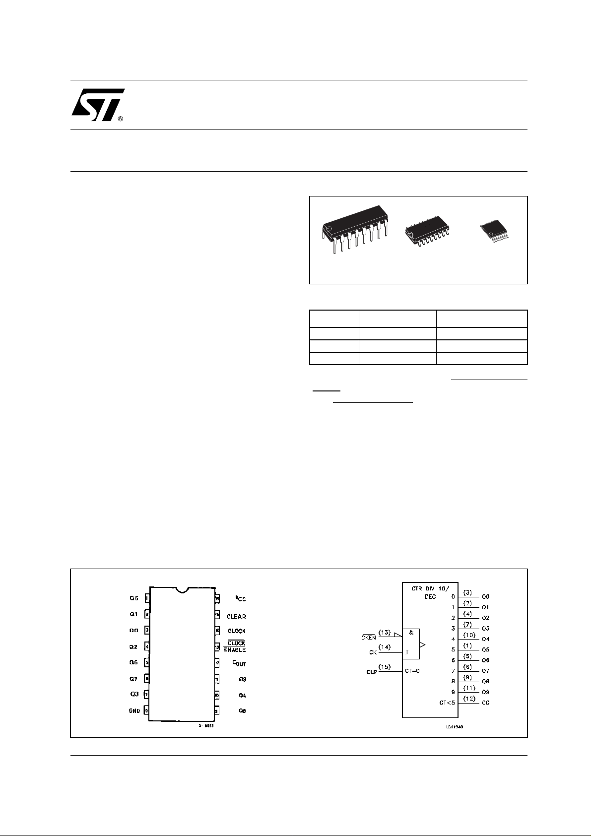
DESCRIPTION
The M74HC4017 is an high speed CMOS
DECADE COUNTER/DIVIDER fabricated with
silicon gate C
2
MOS technology.
The M74HC4017 is a 5-stage Johnson counter
with 10 decoded outputs. Each of the decoded
outputs is normally low and sequentially goes high
on the low to high transition of the clock input.
Each output stays high fo r one clock period of t he
10 clock period cycle. The CARRY output goes
low to high after OUTP UT 10 goes low, and can
TSSOPDIP SOP
ORDER CODES
PACKAGE TUBE T & R
DIP M74HC4017B1R
SOP M74HC4017M1R M74HC4017RM13TR
TSSOP M74HC4017TTR
be used in conjunction with the CL OCK ENAB LE
(CKEN)to cascade several stages.
The CLOCK ENABLE
input disables counting
when in the high st ate. A CLEAR (CLR) input is
also provided which when taken high sets all the
decoded outputs low.
All inputs are equipped with protection circuits
against static discharge and transient excess
voltage.
PIN CONNECTION AND IEC LOGIC SYMBOLS
1/12August 2001
M74HC4017
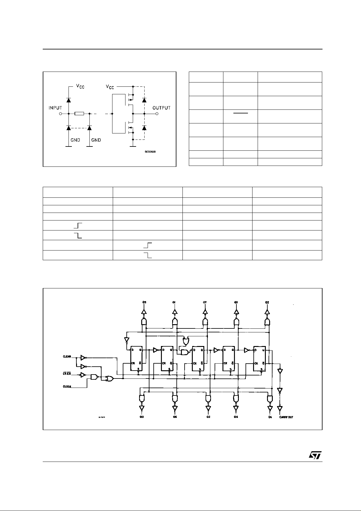
INPUT AND OUTPUT EQUIVALENT CIRCUIT PIN DESCRIPTION
PIN No SYMBOL NAME AND FUNCTION
TRUTH TABLE
CLOCK CLOCK ENABLE CLEAR DECODED OUTPUT(H)
XXHQO
LXLQn
XHLQn
HLQn
H L Qn + 1
X : Don’t Care
Qn : No Ch ange
3, 2, 4, 7, 10,
1, 5, 6, 9, 11
12
13 CKEN
14 CLOCK
15 CL EAR
8 GND Ground (0V)
16 Vcc Positive Supply Voltage
L L Qn + 1
LLQn
Q0 to Q9 Decoded Outputs
C
OUT
Carry Output
(Active LOW)
Clock Enable Input
(Active LOW)
Clock Input (LOW to
HIGH, Edge Triggered)
Master Reset Inputs
(Active HIGH)
LOGIC DIAGRAM
This log i c diagram has not be used to esti m ate propagation delays
2/12
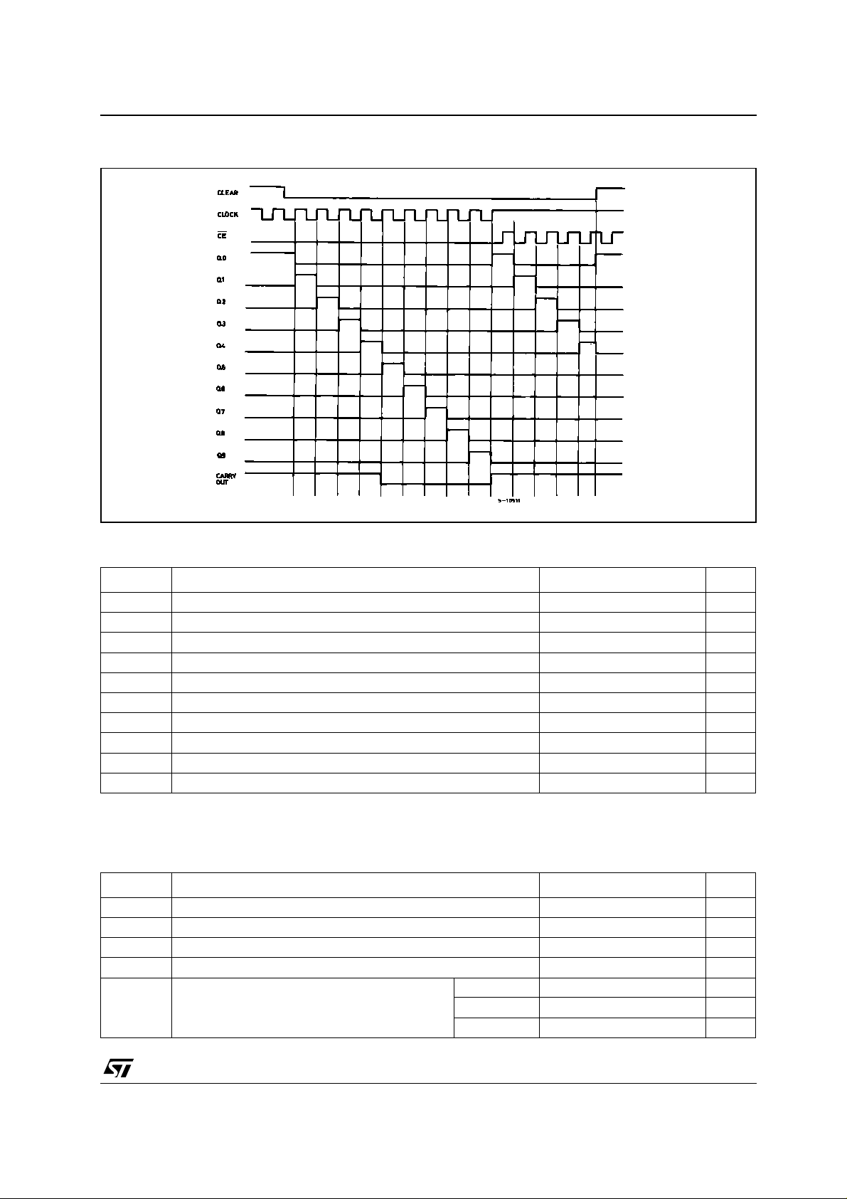
TIMING DIAGRAM
M74HC4017
ABSOLUTE MAXIMUM RATINGS
Symbol Parameter Value Unit
V
V
V
I
I
OK
I
I
or I
CC
P
T
T
Absolute Maximum Ratings are those values beyond which damage to the device may occur. Functional operation under these conditions is
not implied
(*) 500mW at 65
Supply Voltage
CC
DC Input Voltage -0.5 to VCC + 0.5
I
DC Output Voltage -0.5 to VCC + 0.5
O
DC Input Diode Current
IK
DC Output Diode Current
DC Output Current
O
DC VCC or Ground Current
GND
Power Dissipation
D
Storage Temperature
stg
Lead Temperature (10 sec)
L
°C; derate to 300mW by 10mW/°C from 65°C to 85°C
-0.5 to +7 V
V
V
± 20 mA
± 20 mA
± 25 mA
± 50 mA
500(*) mW
-65 to +150 °C
300 °C
RECOMMENDED OPERATING CONDITIONS
Symbol Parameter Value Unit
V
V
V
T
t
r
Supply Voltage
CC
Input Voltage 0 to V
I
Output Voltage 0 to V
O
Operating Temperature
op
Input Rise and Fall Time VCC = 2.0V
, t
f
V
V
CC
CC
= 4.5V
= 6.0V
2 to 6 V
CC
CC
-55 to 125 °C
0 to 1000 ns
0 to 500 ns
0 to 400 ns
V
V
3/12
M74HC4017
DC SPECIFICATIONS
Symbol Parameter
V
V
V
V
I
High Level Input
IH
Voltage
Low Level Input
IL
Voltage
High Level Output
OH
Voltage
Low Level Output
OL
Voltage
I
Input Leakage
I
Current
Quiescent Supply
CC
Current
Test Condition Value
V
(V)
CC
= 25°C
A
Min. Typ. Max. Min. Max. Min. Max.
-40 to 85°C -55 to 125°C
T
2.0 1.5 1.5 1.5
6.0 4.2 4.2 4.2
2.0 0.5 0.5 0.5
6.0 1.8 1.8 1.8
2.0
4.5
6.0
4.5
6.0
2.0
4.5
6.0
4.5
6.0
6.0
6.0
IO=-20 µA
I
=-20 µA
O
I
=-20 µA
O
I
=-4.0 mA
O
I
=-5.2 mA
O
IO=20 µA
I
=20 µA
O
I
=20 µA
O
I
=4.0 mA
O
I
=5.2 mA
O
= VCC or GND
V
I
= VCC or GND
V
I
1.9 2.0 1.9 1.9
4.4 4.5 4.4 4.4
5.9 6.0 5.9 5.9
4.18 4.31 4.13 4.10
5.68 5.8 5.63 5.60
0.0 0.1 0.1 0.1
0.0 0.1 0.1 0.1
0.0 0.1 0.1 0.1
0.17 0.26 0.33 0.40
0.18 0.26 0.33 0.40
± 0.1 ± 1 ± 1 µA
44080µA
Unit
V4.5 3.15 3.15 3.15
V4.5 1.35 1.35 1.35
V
V
4/12
 Loading...