

STMicroelectronics M74HC139 Technical data
M74HC139
DUAL 2 TO 4 DECODER/DEMULTIPLEXER
■ HIGH SPEED:
t
= 13ns (TYP.) at VCC = 6V
PD
■ LOW POWER DISSIPATION:
I
= 4µA(MAX.) at TA=25°C
CC
■ HIGH NOISE IMMUNITY:
V
= V
NIH
■ SYMMETRICAL OUTPUT IMPEDANCE:
|I
| = IOL = 4mA (MIN)
OH
■ BALANCED PROPAGATION DELAYS:
t
≅ t
PLH
■ WIDE OPERATING VOLTAGE RANGE:
V
(OPR) = 2V to 6V
CC
■ PIN AND FUNCTION COMPATIBLE WITH
= 28 % VCC (MIN.)
NIL
PHL
74 SERIES 139
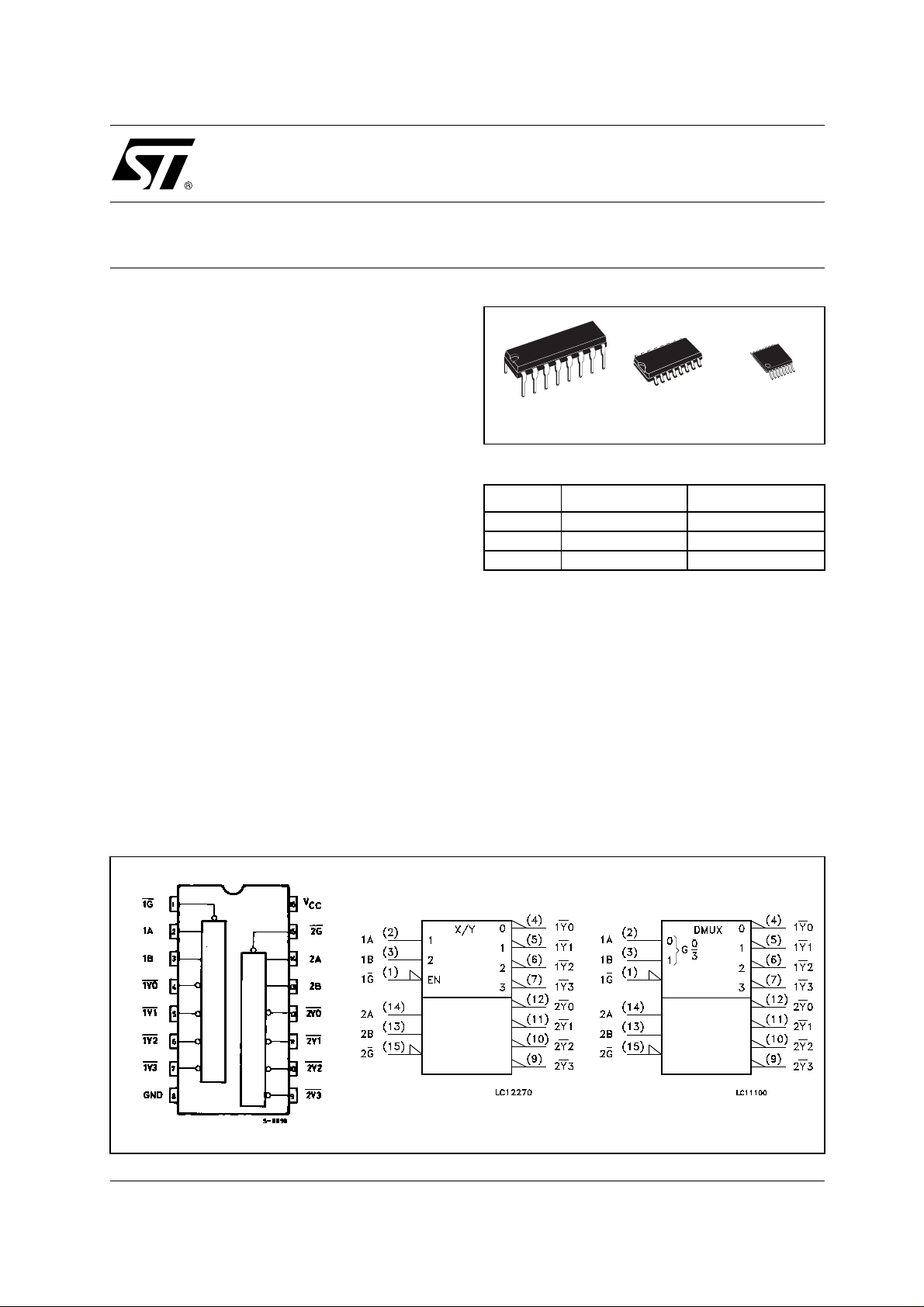
DESCRIPTION
The M74HC139 is an high speed CMOS QUAD
2-INPUT NAND GATE fabricated with silicon gate
2
C
MOS technology.
The active low enable input can be used for gating
or as a data input for demultiplexing applications.
TSSOPDIP SOP
ORDER CODES
PACKAGE TUBE T & R
DIP M74HC139B1R
SOP M74HC139M1R M74HC139RM13TR
TSSOP M74HC139TTR
While the enable input is held high, all four outputs
are high independently of the other inputs.
All inputs are equipped with protection circuits
against static discharge and transient excess
voltage.
PIN CONNECTION AND IEC LOGIC SYMBOLS
1/9July 2001
M74HC139
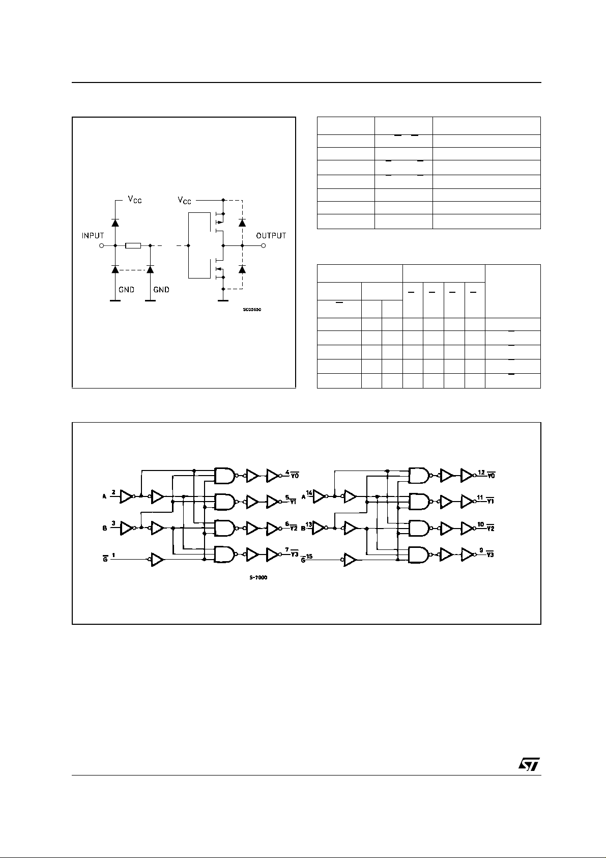
INPUT AND OUTPUT EQUIVALENT CIRCUIT PIN DESCRIPTION
PIN No SYMBOL NAME AND FUNCTION
1, 15 1G
2, 3 1A, 1B Address Inputs
4, 5, 6, 7
12, 11, 10, 9
14, 13 2A, 2B Address Inputs
8 GND Ground (0V)
16
TRUTH TABLE
INPUTS OUTPUTS
ENABLE SELECT
G BA
H X X H H H H NONE
L LLLHHH
LLHHLHH
LHLHHLH
L HHHHHL
, 2G Enable Inputs
TO 1Y
1Y
0
TO 2Y
2Y
0
V
CC
Y
Outputs
3
Outputs
3
Positive Supply Voltage
0Y1Y2Y3
SELECTED
OUTPUT
Y
0
Y
1
Y
2
Y
3
LOGIC DIAGRAM
This log i c diagram has not be used to est i m at e propagation delays
2/9
M74HC139
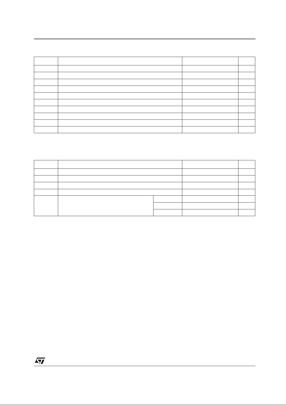
ABSOLUTE MAXIMUM RATINGS
Symbol Parameter Value Unit
V
V
V
I
I
OK
I
I
or I
CC
P
T
T
Absolute Maximum Ratings are those values beyond which damage to the device may occur. Functional operation under these conditions is
not implied
(*) 500mW at 65
RECOMMENDED OPERATING CONDITIONS
Symbol Parameter Value Unit
V
V
V
T
t
r
Supply Voltage
CC
DC Input Voltage -0.5 to VCC + 0.5
I
DC Output Voltage -0.5 to VCC + 0.5
O
DC Input Diode Current
IK
DC Output Diode Current
DC Output Current
O
DC VCC or Ground Current
GND
Power Dissipation
D
Storage Temperature
stg
Lead Temperature (10 sec)
L
°C; derate to 300mW by 10mW/°C from 65°C to 85°C
Supply Voltage
CC
Input Voltage 0 to V
I
Output Voltage 0 to V
O
Operating Temperature
op
Input Rise and Fall Time VCC = 2.0V
, t
f
V
V
CC
CC
= 4.5V
= 6.0V
-0.5 to +7 V
V
V
± 20 mA
± 20 mA
± 25 mA
± 50 mA
500(*) mW
-65 to +150 °C
300 °C
2 to 6 V
CC
CC
V
V
-55 to 125 °C
0 to 1000 ns
0 to 500 ns
0 to 400 ns
3/9
 Loading...