

M5450
M5451
LED DISPLAY DRIVERS
FEATURES SUMMARY
■ M5450 34 OUTPUTS/15mA SINK
■ M5451 35 OUTPUTS/15mA SINK
■ CURRENT GENERATOR OUTPUTS (NO
EXTERNAL RESISTORS REQUIRED)
■
CONTINUOUS BRIGHTNESS CONTROL
■ SERIAL DATA INPUT
■ ENABLE (ON M5450)
■ WIDE SUPPLY VOLTAGE OPERATION
■ TTL COMPATIBILITY
Application Examples:
■ MICROPROCESSOR DISPLAYS
■ INDUSTRIAL CONTROL INDICATOR
■ RELAY DRIVER
■ INSTRUMENTATION READOUTS
DESCRIPTION
The M5450 and M5451 are monolithic MOS integrated circuits produced with an N-channel silicon
gate technology. They are available in 40-pin dual
in-line plastic packages.
A single pin controls the LED display brightness by
setting a reference current through a variable resistor connected to V
or to a separate supply of
DD
13.2V maximum.
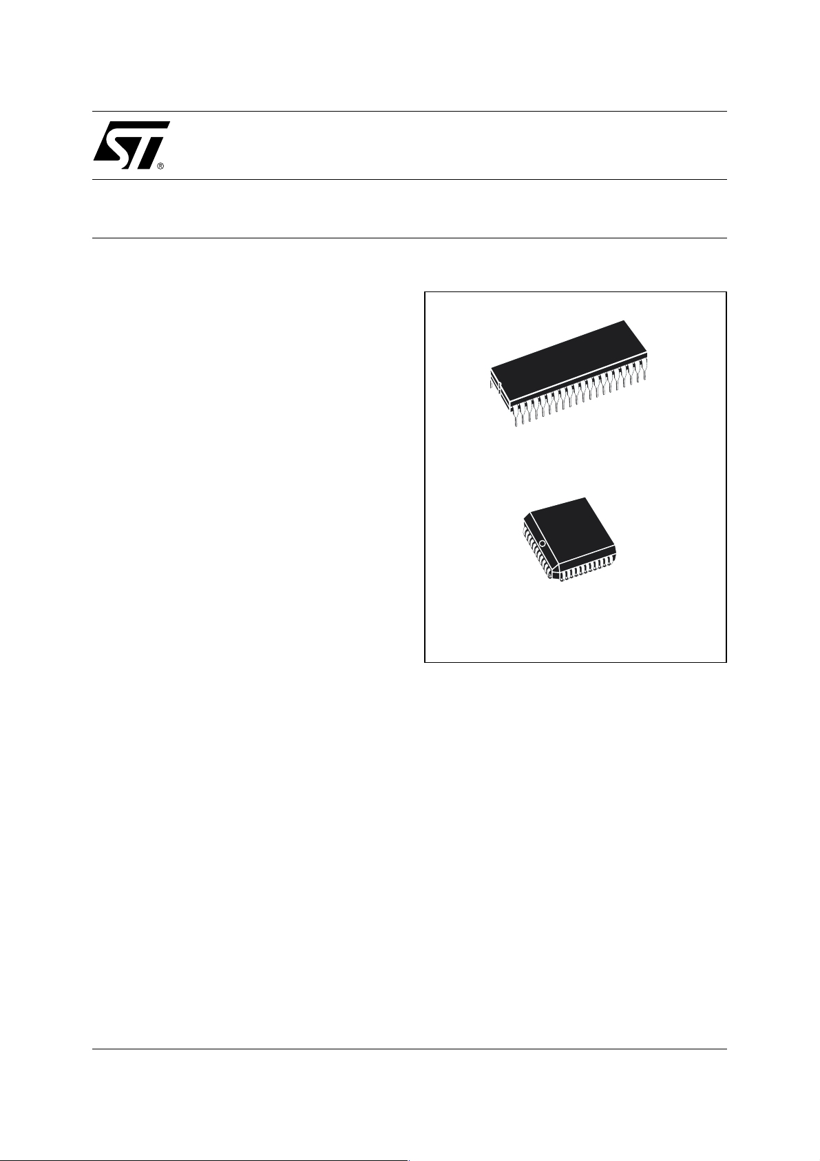
Figure 1. Packages
40
1
PDIP40
(Plastic Package)
PLCC44
(Plastic Chip Carrier)
REV. 2
1/12April 2004

M5450, M5451
Figure 2. Pin Connection
1
V
OUTPUT BIT 9
OUTPUT BIT 8
OUTPUT BIT 7
OUTPUT BIT 6
OUTPUT BIT 5
OUTPUT BIT 4
OUTPUT BIT 3
OUTPUT BIT 2
OUTPUT BIT 1
SS
2
3
4
5
6
7
8
9
10
11
12
13
14
15
16
17
18
19
20
DD
OUTPUT BIT 17
OUTPUT BIT 16
OUTPUT BIT 15
OUTPUT BIT 14
OUTPUT BIT 13
OUTPUT BIT 12
OUTPUT BIT 11
OUTPUT BIT 10
BRIGHTNESS CONTROL
Figure 3. Block Diagram
BRIGTHNESS
40
39
38
37
36
35
34
33
32
31
30
29
28
27
26
25
24
23
22
21
CONTROL
100kΩ
OUTPUT BIT 18
OUTPUT BIT 19
OUTPUT BIT 20
OUTPUT BIT 21
OUTPUT BIT 22
OUTPUT BIT 23
OUTPUT BIT 24
OUTPUT BIT 25
OUTPUT BIT 26
OUTPUT BIT 27
OUTPUT BIT 28
OUTPUT BIT 29
OUTPUT BIT 30
OUTPUT BIT 31
OUTPUT BIT 32
OUTPUT BIT 33
OUTPUT BIT 34
DATA ENABLE FOR M5450
OUTPUT BIT 35 FOR M5451
DATA IN
CLOCK INV
19
V
DD
OUTPUT
BIT 34
20 24
OUTPUT BIT 13
OUTPUT BIT 12
OUTPUT BIT 11
OUTPUT BIT 10
OUTPUT BIT 9
OUTPUT BIT 8
OUTPUT BIT 7
OUTPUT BIT 6
OUTPUT BIT 5
OUTPUT BIT 4
7
8
9
10
11
12
N.C.
13
14
15
16
17 29
OUTPUT
BIT 1
18
35 OUTPUT BUFFERS
OUTPUT BIT 14
6
18
OUTPUT BIT 3
SS
OUTPUT BIT 15
OUTPUT BIT 16
OUTPUT BIT 17
OUTPUT BIT 18
V
N.C
12345
44
192021222324252627
DD
N.C
V
CLOCK IN
OUTPUT BIT 2
OUTPUT BIT 1
BRIGHTNESS CONTROL
OUTPUT BIT 22
OUTPUT BIT 19
OUTPUT BIT 20
OUTPUT BIT 21
40
41
42
43
39
38
37
36
35
34
33
32
31
30
28
DATA IN
OUTPUT BIT 33
OUTPUT BIT 34
OUTPUT BIT 35
OUTPUT BIT 23
OUTPUT BIT 24
OUTPUT BIT 25
OUTPUT BIT 26
OUTPUT BIT 27
N.C.
OUTPUT BIT 28
OUTPUT BIT 29
OUTPUT BIT 30
OUTPUT BIT 31
OUTPUT BIT 32
2/12
DATA ENABLE (M5450)
OUTPUT35 (5451)
SERIAL
DATA
CLOCK
35 LATCHES
LOAD
23
22
21
35-BIT SHIFT REGISTER
RESET
1
M5450, M5451
Table 1. Absolute Maximum Ratings
Symbol Parameter Value Unit
V
DD
V
I
V
O(off)
I
O
P
TOT
T
j
T
OP
T
STG
Note: Stresses above those listed under "Absolute Maximum Ratings" may causes permanent damage to the device. This is a stress rating
only and functional operation of the device at these or any other conditions above those indicated in the operational sections of this
specification is not implied. Exposure to absolute maximum rating conditions for extended periods may affect device reliability.
FUNCTIONAL DESCRIPTION
Both the M5450 and the M5451 are specially designed to operate 4 or 5-digit alphanumeric displays with minimal interface with the display and
the data source. Serial data transfer from the data
source to the display driver is accomplished with 2
signals, serial data and clock. Using a format of a
leading "1" followed by the 35 data bits allows data
transfer without an additional load signal. The 35
data bits are latched after the 36th bit is complete,
thus providing non-multiplexed, direct drive to the
display.
Outputs change only if the serial data bits differ
from the previous time.
Display brightness is determined by control of the
output current LED displays.
A 1nF capacitor should be connected to brightness control, pin 19, to prevent possible oscillations.
A block diagram is shown in Figure 3. For the
M5450 a DATA ENABLE
35th output. The DATA ENABLE
option for the M5450.
The output current is typically 20 times greater
than the current into pin 19, which is set by an external variable resistor. There is an internal limiting
resistor of 400W nominal value.
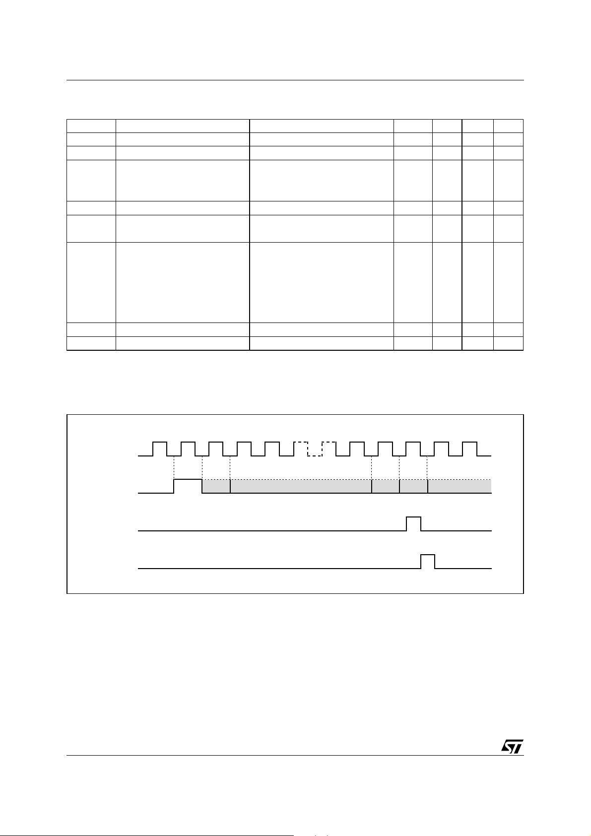
Figure 4 shows the input data format. A start bit of
logical "1" precedes the 35 bits of data. At the 36th
clock a LOAD signal is generated synchronously
with the high state of the clock, which loads the 35
bits of the shift registers into the latches.
At the low state of the clock a RESET signal is
generated which clears all the shift registers for
the next set of data. The shift registers are static
Supply Voltage – 0.3 to 15 V
Input Voltage – 0.3 to 15 V
Off State Output Voltage 15 V
Output Sink Current 40 mA
Total Package Power Dissipation at 25°C 1 W
Total Package Power Dissipation at 85°C 560 mW
Junction Temperature 150 °C
Operating Temperature Range – 25 to 85 °C
Storage Temperature Range – 65 to 150 °C
master-slave configurations. There is no clear for
the master portion of the first shift register, thus allowing continuous operation.
There must be a complete set of 36 clocks or the
shift registers will not clear.
When power is first applied to the chip an internal
power ON reset signal is generated which resets
all registers and all latches. The START bit and the
first clock return the chip to its normal operation.
Bit 1 is the first bit following the start bit and it will
appear on Pin 18. A logical "1" at the input will turn
on the appropriate LED.
Figure 5 shows the timing relationship between
Data, Clock and DATA ENABLE
.
A max clock frequency of 0.5MHz is assumed. For
applications where a lesser number of outputs are
used, it is possible to either increase the current
per output or operate the part at higher than 1V
.
V
is used instead of the
input is a metal
OUT
The following equation can be used for calculations.
= [(V
T
j
7mA)] (124°C/W) + T
OUT
) (I
) (No. of segments) + (VDD ×
LED
amb
where :
T
= junction temperature (150°C max)
j
= the voltage at the LED driver outputs
V
OUT
= the LED current
I
LED
124°C/W = thermal coefficient of the package
T
= ambient temperature
amb
The above equation was used to plot Figure 6, Figure 7 and Figure 8.
3/12
M5450, M5451
Table 2. Static Electrical Characteristics
within operating range, VDD = 4.75V to 13.2V, VSS = 0V, unless otherwise specified)
(T
amb
Symbol Parameter Test Conditions Min. Typ. Max. Unit
V
DD
I
DD
V
I
V
V
O(off)
I
f
clock
I
Note: 1. Output matching is calculated as the percent variation from I
2. With a fixed resistor on the brightness input some variation in brightness will occur from one device to another.
3. Absolute maximum for each output should be limited to 40mA.
4. The VO voltage should be regulated by the user. See Figure 7 and Figure 8 for allowable VO versus IO operation.
Supply Voltage 4.75 13.2 V
V
Supply Current
Input Voltage Logical "0" Level ± 10µA Input Bias - 0.3 0.8 V
I
Logical "1" Level
Brightness Input Current (note 2) 0 0.75 mA
B
Brightness Input Voltage (pin 19)
B
= 13.2V
DD
4.75 ≤ V
V
DD
Input Current = 750µA, T
DD
≤ 5.25
2.2
> 5.25 VDD - 2 V
amb
= 25°C
34.3V
Off State Out. Voltage 13.2 V
Out. Sink Current (note 3)
O
V
Segment OFF
Segment ON
= 3V
O
V
= 1V (note 4)
O
Brightness In. = 0µA010µA
Brightness In. = 100µ 2 274mA
Brightness In. = 750µA121525mA
Input Clock Frequency 0 0.5 MHz
Output Matching (note 1) ± 20 %
O
+ I
MIN
/2.
MAX
7mA
V
DD
DD
10 µA
V
V
Figure 4. Input Data Format
1
CLOCK
START
DATA
LOAD
(INTERNAL)
RESET
(INTERNAL)
BIT 1
BIT 34
36
BIT 35
4/12
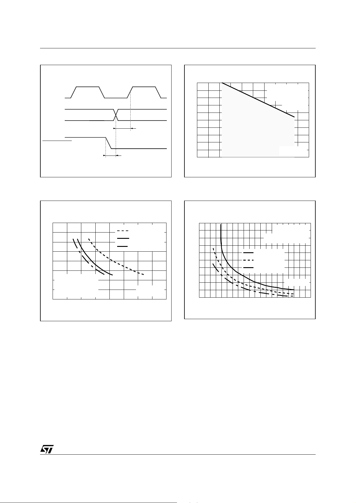
Figure 5. Figure 6.
P (W)
tot
1.0
CLOCK
DATA
0.8
0.6
M5450, M5451
15mA/segment
34 segments
V = 1V
O
300ns (min.)
DATA ENABLE
100ns (min.)
0.4
0.2
0
Figure 7. Figure 8.
I0 (mA)
105
85
65
3.2
2.8
2.4
2.0
VO (V)
20 segments
30 segments
34 segments
1.6
1.2
0.8
T
amb
0.4
Tj = 150˚C (max.) ˚
= 85˚C
I
LED
(mA)
45
25
5
4
8121620240
28 32
0
SAFE OPERATING
AREA
T
amb
20 40 60 80 100
T
= 85˚C
amb
I
O (max.)
= 40mA
VO = 1V
= 1.5V
V
O
= 2V
V
O
N˚ Segm.
48
12 16
20 24 28 32
(˚C)
36
40
5/12

M5450, M5451
TYPICAL APPLICATIONS
Figure 9. Basic Electronically Tuned Radio Or Tv System
AM
FM
34 SEGMENTS
M5450
DISPLAY
DRIVER
KEYBOARD
ELECTRONIC
CONTROLLER
DETEC. ETC.
Figure 10. Duplexing 8 Digits With One M5450
V
DD
V
LED
.
916 2840 3239 2431
.
.
TUNING
STATION
....
PLL
SYNTHESIZER
V
LED
V
DD
.
6/12
CLOCK IN
DATA IN
211822
BRIGHTNESS
CONTROL
M5450
19
1 23
17
20
V
DD

POWER DISSIPATION OF THE IC
The power dissipation of the IC can be limited using different configurations.
Figure 11- In the application R must be chosen
taking into account the worst operating conditions.
Figure 11.
+V
C
R
I
D
V
D
V
OUT
M5450, M5451
The total power dissipation of the IC depends, in a
first approximation, only on the number of segments activated.
Figure 12.
+V
C
R is determined by the maximum number of segments activated
VCV
– V
------------------------------------------- ---------------------=
R
DMAX
N
MAXLD
–
OMIN
The worst case condition for the device is when
roughly half of the maximum number of segments
are activated.
It must be checked that the total power dissipation
does not exceed the absolute maximum ratings of
the device.
In critical cases more resistors can be used in conjunction with groups of segments.
In this case the current variation in the single resistor is reduced and P
limited.
tot
Figure 12 - In this configuration the drop on the serial connected diodes is quite stable if the diodes
are properly chosen.
Figure 13 - In this configuration V
+ VD is con-
OUT
stant. The total power dissipation of the IC depends only on the number of segments activated.
Figure 13.
+V
C
V
+V
OUT
D
7/12

M5450, M5451
PART NUMBERING
Table 3. Order Codes
Part Number Package Temperature Range
M5450B7/M5451B7 PDIP40 -25 to 85 °C
M5451Q PLCC44 -25 to 85 °C
8/12

PACKAGE MECHANICAL
Table 4. PDIP40 - Mechanical Data
millimeters inches
Symbol
Typ Min Max Typ Min Max
a1 0.63 0.025
b 0.45 0.018
b1 0.23 0.31 0.009 0.012
b2 1.27 0.050
D 52.58 2.070
E 15.2 16.68 0.598 0.657
e 2.54 0.100
e3 48.26 1.900
F 14.1 0.555
i 4.445 0.175
L 3.3 0.130
M5450, M5451
Figure 14. PDIP40 - Package Dimensions
b
b2
e3
D
40
120
a1
I
L
b1
e
E
21
F
Note: Drawing is not to scale
9/12

M5450, M5451
Table 5. PLCC44 - Mechanical Data
Symbol
Typ Min Max Typ Min Max
A 17.4 17.65 0.685 0.695
B 16.51 16.65 0.650 0.656
C 3.65 3.7 0.144 0.146
D 4.2 4.57 0.165 0.180
d1 2.59 2.74 0.102 0.108
d2 0.68 0.027
E 14.99 16 0.590 0.630
e 1.27 0.050
e3 12.7 0.500
F 0.46 0.018
F1 0.71 0.028
G 0.101 0.004
M 1.16 0.046
M1 1.14 0.045
millimeters inches
Figure 15. PLCC44 - Package Dimensions
B
M1
21
A
M1
6
7
17
18
C
M
3944
38
FeF1
e3
E
29
28
M
d2
d1
G
(Seating Plane Coplanarity)
D
Note: Drawing is not to scale.
10/12

REVISION HISTORY
Table 6. Revision History
Date Revision Description of Changes
September-1993 1 First Issue
14-Mar-2004 2 Stylesheet update. No content change.
M5450, M5451
11/12

M5450, M5451
Information furnished is believed to be accurate and reliable. However, STMicroelectronics assumes no responsibility for the consequences
of use of such information nor for any infringement of patents or other rights of third parties which may result from its use. No license is granted
by implication or otherwise under any patent or patent rights of STMicroelectronics. Specifications mentioned in this publication are subject
to change without notice. This publication supersedes and replaces all information previously supplied. STMicroelectronics products are not
authorized for use as critical components in life support devices or systems without express written approval of STMicroelectronics.
The ST logo is a registered trademark of STMicroelectronics.
All other names are the property of their respective owners
© 2004 STMicroelectronics - All rights reserved
STMicroelectronics GROUP OF COMPANIES
Australia - Belgium - Brazil - Canada - China - Czech Republic - Finland - France - Germany - Hong Kong - India - Israel - Italy - Japan -
Malaysia - Malta - Morocco - Singapore - Spain - Sweden - Switzerland - United Kingdom - United States
www.st.com
12/12
 Loading...