

Page 1
FEAT URES SUMMARY
■ DROP-IN REPLACEMENT FOR PC
COMPUTER CLOCK/CALENDAR
■ COUNTS SECONDS, MINUTES, HOURS,
DAYS, DAY OF THE WEE K, DA TE, MO NTH,
and YEAR WITH LEAP YEAR
COMPENSATION
■ INTERFACED WITH SOFTWARE AS 128
RAM LOCATIONS:
– 14 Bytes of Clock and Control Registers
– 114 Bytes of General Purpose RAM
■ SELECTABLE BUS TIMING (Intel/Motorola)
■ THREE INTERRUPTS ARE SEPARATELY
SOFTWARE-MASKABL E and TESTABLE
– Time-of-Day Alarm (Once/Second to
Once/Day)
– Periodic Rates from 122µs to 500ms
– End-of-Clock Update Cycle
■ PROGRAMMABLE SQUA RE WAVE
OUTPUT
■ 10 YEARS OF DATA RETENTION AND
CLOCK OPERATION IN THE ABSENCE O F
POWER
■ SELF-CONTAINED BATTERY AND
CRYSTAL IN THE CAPHAT DIP PACKAG E
■ PACKAGING INCLUDES A 28-LEAD SOIC
and SNAPHAT
separately)
■ SOIC PACKAGE PROVIDES DIRECT
CONNECTION FOR A SNAPHAT TOP
CONTAINS THE BATTERY AND CRYSTAL
■ PIN AND FUNCTION COMPATIBLE WITH
bq3285/7A and DS12887
®
TOP (to be ordered
M48T86
5.0V PC Real-Ti me Clock
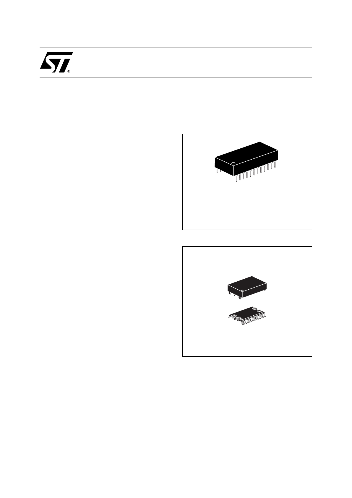
Figure 1. 24-pin PCDIP, CAPHAT™ Package
24
1
PCDIP24 (PC)
Battery/Crystal
CAPHAT
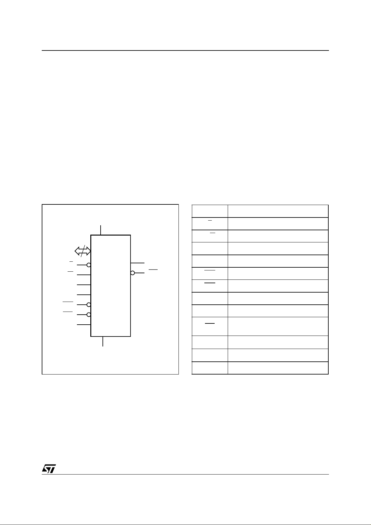
Figure 2. 28-pi n S O I C Package
SNAPHAT (SH)
Battery/Crystal
28
1
SOH28 (MH)
1/29April 2004
Page 2

M48T86
TABLE OF CONTENTS
FEATURES SUMMARY . . . . . . . . . . . . . . . . . . . . . . . . . . . . . . . . . . . . . . . . . . . . . . . . . . . . . . . . . . . . . 1
Figure 1. 24-pin PCDIP, CAPHAT™ Package . . . . . . . . . . . . . . . . . . . . . . . . . . . . . . . . . . . . . . . . . 1
Figure 2. 28-pin SOIC Package . . . . . . . . . . . . . . . . . . . . . . . . . . . . . . . . . . . . . . . . . . . . . . . . . . . . 1
SUMMARY DESCRIPTION. . . . . . . . . . . . . . . . . . . . . . . . . . . . . . . . . . . . . . . . . . . . . . . . . . . . . . . . . . . 5
Figure 3. Logic Diagram . . . . . . . . . . . . . . . . . . . . . . . . . . . . . . . . . . . . . . . . . . . . . . . . . . . . . . . . . . 5
Table 1. Signal Names . . . . . . . . . . . . . . . . . . . . . . . . . . . . . . . . . . . . . . . . . . . . . . . . . . . . . . . . . . 5
Figure 4. 24-pin DIP Connections. . . . . . . . . . . . . . . . . . . . . . . . . . . . . . . . . . . . . . . . . . . . . . . . . . . 6
Figure 5. 28-pin SOIC Connections . . . . . . . . . . . . . . . . . . . . . . . . . . . . . . . . . . . . . . . . . . . . . . . . . 6
Figure 6. Block Diagram . . . . . . . . . . . . . . . . . . . . . . . . . . . . . . . . . . . . . . . . . . . . . . . . . . . . . . . . . . 6
OPERATION . . . . . . . . . . . . . . . . . . . . . . . . . . . . . . . . . . . . . . . . . . . . . . . . . . . . . . . . . . . . . . . . . . . . . . 7
Signal Description. . . . . . . . . . . . . . . . . . . . . . . . . . . . . . . . . . . . . . . . . . . . . . . . . . . . . . . . . . . . . . 7
V
, VSS.. . . . . . . . . . . . . . . . . . . . . . . . . . . . . . . . . . . . . . . . . . . . . . . . . . . . . . . . . . . . . . . . . . . . . . 7
CC
SQW (Square Wave Output). . . . . . . . . . . . . . . . . . . . . . . . . . . . . . . . . . . . . . . . . . . . . . . . . . . . . . . 7
AD0-AD7 (Multiplexed Bi-Directional Address/Data Bus). . . . . . . . . . . . . . . . . . . . . . . . . . . . . . . . . 7
AS (Address Strobe Input). . . . . . . . . . . . . . . . . . . . . . . . . . . . . . . . . . . . . . . . . . . . . . . . . . . . . . . . . 7
MOT (Mode Select). . . . . . . . . . . . . . . . . . . . . . . . . . . . . . . . . . . . . . . . . . . . . . . . . . . . . . . . . . . . . . 7
DS (Data Strobe Input).. . . . . . . . . . . . . . . . . . . . . . . . . . . . . . . . . . . . . . . . . . . . . . . . . . . . . . . . . . . 7
E
(Chip Enable Input). . . . . . . . . . . . . . . . . . . . . . . . . . . . . . . . . . . . . . . . . . . . . . . . . . . . . . . . . . . . . 8
IRQ
(Interrupt Request Output). . . . . . . . . . . . . . . . . . . . . . . . . . . . . . . . . . . . . . . . . . . . . . . . . . . . . 8
RST
(Reset Input).. . . . . . . . . . . . . . . . . . . . . . . . . . . . . . . . . . . . . . . . . . . . . . . . . . . . . . . . . . . . . . . 8
RCL
(RAM Clear). . . . . . . . . . . . . . . . . . . . . . . . . . . . . . . . . . . . . . . . . . . . . . . . . . . . . . . . . . . . . . . . 8
R/W
(READ/WRITE Input). . . . . . . . . . . . . . . . . . . . . . . . . . . . . . . . . . . . . . . . . . . . . . . . . . . . . . . . . 8
Non-Volatile RAM . . . . . . . . . . . . . . . . . . . . . . . . . . . . . . . . . . . . . . . . . . . . . . . . . . . . . . . . . . . . . . 8
Figure 7. Intel Bus READ AC Waveform . . . . . . . . . . . . . . . . . . . . . . . . . . . . . . . . . . . . . . . . . . . . . 8
Figure 8. Intel Bus WRITE Mode AC Waveform. . . . . . . . . . . . . . . . . . . . . . . . . . . . . . . . . . . . . . . .9
Figure 9. M oto rola Bus READ/WRITE Mode AC Waveforms. . . . . . . . . . . . . . . . . . . . . . . . . . . . . . 9
Table 2. AC Characteristics. . . . . . . . . . . . . . . . . . . . . . . . . . . . . . . . . . . . . . . . . . . . . . . . . . . . . . 10
CLOCK OPERATIONS . . . . . . . . . . . . . . . . . . . . . . . . . . . . . . . . . . . . . . . . . . . . . . . . . . . . . . . . . . . . . 11
Address Map . . . . . . . . . . . . . . . . . . . . . . . . . . . . . . . . . . . . . . . . . . . . . . . . . . . . . . . . . . . . . . . . . 11
Time, Calendar, and Alarm Locations. . . . . . . . . . . . . . . . . . . . . . . . . . . . . . . . . . . . . . . . . . . . . 11
Figure 10.Address Map. . . . . . . . . . . . . . . . . . . . . . . . . . . . . . . . . . . . . . . . . . . . . . . . . . . . . . . . . . 11
Table 3. Ti me , Calendar, and Alarm Formats . . . . . . . . . . . . . . . . . . . . . . . . . . . . . . . . . . . . . . . . 12
Interrupts . . . . . . . . . . . . . . . . . . . . . . . . . . . . . . . . . . . . . . . . . . . . . . . . . . . . . . . . . . . . . . . . . . . . 12
Periodic Interrupt. . . . . . . . . . . . . . . . . . . . . . . . . . . . . . . . . . . . . . . . . . . . . . . . . . . . . . . . . . . . . . 13
Alarm Interrupt. . . . . . . . . . . . . . . . . . . . . . . . . . . . . . . . . . . . . . . . . . . . . . . . . . . . . . . . . . . . . . . . 13
Update Cycle Interrupt . . . . . . . . . . . . . . . . . . . . . . . . . . . . . . . . . . . . . . . . . . . . . . . . . . . . . . . . . 13
Oscillator Control Bits . . . . . . . . . . . . . . . . . . . . . . . . . . . . . . . . . . . . . . . . . . . . . . . . . . . . . . . . . 1 3
Update Cycle . . . . . . . . . . . . . . . . . . . . . . . . . . . . . . . . . . . . . . . . . . . . . . . . . . . . . . . . . . . . . . . . . 13
Square Wave Output Se lection . . . . . . . . . . . . . . . . . . . . . . . . . . . . . . . . . . . . . . . . . . . . . . . . . .14
Table 4. S quare Wave Frequency/Periodic Interrupt Rate . . . . . . . . . . . . . . . . . . . . . . . . . . . . . . 14
2/29
Page 3

M48T86
Register A. . . . . . . . . . . . . . . . . . . . . . . . . . . . . . . . . . . . . . . . . . . . . . . . . . . . . . . . . . . . . . . . . . . . 15
UIP. Update in Progress . . . . . . . . . . . . . . . . . . . . . . . . . . . . . . . . . . . . . . . . . . . . . . . . . . . . . . . . . 15
OSC0, OSC1, OSC2. Oscillator Control . . . . . . . . . . . . . . . . . . . . . . . . . . . . . . . . . . . . . . . . . . . . . 15
RS3, RS2, RS1, RS0. . . . . . . . . . . . . . . . . . . . . . . . . . . . . . . . . . . . . . . . . . . . . . . . . . . . . . . . . . . . 15
Table 5. REGISTER A MSB . . . . . . . . . . . . . . . . . . . . . . . . . . . . . . . . . . . . . . . . . . . . . . . . . . . . . 15
Figure 11.Update Period Timing and UIP . . . . . . . . . . . . . . . . . . . . . . . . . . . . . . . . . . . . . . . . . . . . 15
Register B. . . . . . . . . . . . . . . . . . . . . . . . . . . . . . . . . . . . . . . . . . . . . . . . . . . . . . . . . . . . . . . . . . . . 16
SET . . . . . . . . . . . . . . . . . . . . . . . . . . . . . . . . . . . . . . . . . . . . . . . . . . . . . . . . . . . . . . . . . . . . . . . . . 16
PIE: Periodic Interrupt Enable. . . . . . . . . . . . . . . . . . . . . . . . . . . . . . . . . . . . . . . . . . . . . . . . . . . . . 1 6
AIE: Alarm Interrupt Enable. . . . . . . . . . . . . . . . . . . . . . . . . . . . . . . . . . . . . . . . . . . . . . . . . . . . . . . 16
UIE: Update Ended Interrupt Enable. . . . . . . . . . . . . . . . . . . . . . . . . . . . . . . . . . . . . . . . . . . . . . . .16
SQWE: Square Wave Enable . . . . . . . . . . . . . . . . . . . . . . . . . . . . . . . . . . . . . . . . . . . . . . . . . . . . . 16
DM: Data Mode. . . . . . . . . . . . . . . . . . . . . . . . . . . . . . . . . . . . . . . . . . . . . . . . . . . . . . . . . . . . . . . .16
24/12 . . . . . . . . . . . . . . . . . . . . . . . . . . . . . . . . . . . . . . . . . . . . . . . . . . . . . . . . . . . . . . . . . . . . . . . . 16
DSE. Daylight Savings Enable . . . . . . . . . . . . . . . . . . . . . . . . . . . . . . . . . . . . . . . . . . . . . . . . . . .16
Table 6. REGISTER B MSB . . . . . . . . . . . . . . . . . . . . . . . . . . . . . . . . . . . . . . . . . . . . . . . . . . . . . 16
Figure 12.Update-ended/Periodic Interrupt Relationship . . . . . . . . . . . . . . . . . . . . . . . . . . . . . . . . 17
Register C. . . . . . . . . . . . . . . . . . . . . . . . . . . . . . . . . . . . . . . . . . . . . . . . . . . . . . . . . . . . . . . . . . . . 18
IRQF: Interrupt Request Flag . . . . . . . . . . . . . . . . . . . . . . . . . . . . . . . . . . . . . . . . . . . . . . . . . . . . . 18
PF: Periodic Interrupt Flag. . . . . . . . . . . . . . . . . . . . . . . . . . . . . . . . . . . . . . . . . . . . . . . . . . . . . . . . 18
AF: Alarm Flag. . . . . . . . . . . . . . . . . . . . . . . . . . . . . . . . . . . . . . . . . . . . . . . . . . . . . . . . . . . . . . . . . 18
UF: Update Ended Interrupt Flag . . . . . . . . . . . . . . . . . . . . . . . . . . . . . . . . . . . . . . . . . . . . . . . . . . 18
BIT 0 through 3: Unused Bits . . . . . . . . . . . . . . . . . . . . . . . . . . . . . . . . . . . . . . . . . . . . . . . . . . . . . 1 8
Register D. . . . . . . . . . . . . . . . . . . . . . . . . . . . . . . . . . . . . . . . . . . . . . . . . . . . . . . . . . . . . . . . . . . . 18
VRT: Valid Ram And Time . . . . . . . . . . . . . . . . . . . . . . . . . . . . . . . . . . . . . . . . . . . . . . . . . . . . . . . 18
BIT 0 through 6: Unused Bits . . . . . . . . . . . . . . . . . . . . . . . . . . . . . . . . . . . . . . . . . . . . . . . . . . . . . 1 8
Table 7. REGISTER C MSB . . . . . . . . . . . . . . . . . . . . . . . . . . . . . . . . . . . . . . . . . . . . . . . . . . . . . 18
Table 8. REGISTER D MSB . . . . . . . . . . . . . . . . . . . . . . . . . . . . . . . . . . . . . . . . . . . . . . . . . . . . . 18
V
Noise And Negative Going Transients. . . . . . . . . . . . . . . . . . . . . . . . . . . . . . . . . . . . . . . . . 19
CC
Figure 13.Supply Voltage Protection. . . . . . . . . . . . . . . . . . . . . . . . . . . . . . . . . . . . . . . . . . . . . . . . 19
MAXIMUM RATING. . . . . . . . . . . . . . . . . . . . . . . . . . . . . . . . . . . . . . . . . . . . . . . . . . . . . . . . . . . . . . . . 20
Table 9. Absolute Maximum Ratings. . . . . . . . . . . . . . . . . . . . . . . . . . . . . . . . . . . . . . . . . . . . . . . 20
DC AND AC PARAMETERS. . . . . . . . . . . . . . . . . . . . . . . . . . . . . . . . . . . . . . . . . . . . . . . . . . . . . . . . . 21
Table 10.Operating and AC Measurement Conditions . . . . . . . . . . . . . . . . . . . . . . . . . . . . . . . . . . 21
Figure 14.AC Testing Load Circuit (No IRQ). . . . . . . . . . . . . . . . . . . . . . . . . . . . . . . . . . . . . . . . . . 21
Figure 15.AC Testing Load Circuit (with IRQ). . . . . . . . . . . . . . . . . . . . . . . . . . . . . . . . . . . . . . . . . 21
Table 11.Capacitance. . . . . . . . . . . . . . . . . . . . . . . . . . . . . . . . . . . . . . . . . . . . . . . . . . . . . . . . . . . 21
Table 12.DC Characteristics . . . . . . . . . . . . . . . . . . . . . . . . . . . . . . . . . . . . . . . . . . . . . . . . . . . . . . 22
Figure 16.Power Down/Up Mode AC Waveforms. . . . . . . . . . . . . . . . . . . . . . . . . . . . . . . . . . . . . . 22
Table 13.Power Down/Up Mode AC Characteristics . . . . . . . . . . . . . . . . . . . . . . . . . . . . . . . . . . . 22
Table 14. Power Down/Up Trip Points DC Characteristics. . . . . . . . . . . . . . . . . . . . . . . . . . . . . 22
PACKAGE MECHANICAL INFORMATION . . . . . . . . . . . . . . . . . . . . . . . . . . . . . . . . . . . . . . . . . . . . . 23
Figure 17.PCDIP24 – 24-pin Plastic DIP, battery CAPHAT, Package Outline . . . . . . . . . . . . . . . . 23
3/29
Page 4

M48T86
Table 15. PCDIP24 – 24-pin Plastic DIP, battery CAPHAT, Package Mechanical Data. . . . . . . . . 23
Figure 18.SOH28 – 28-lead Plastic Small Outline, 4-socket SNAPHAT, Package Outline. . . . . . . 24
Table 16. SOH28 – 28-lead Plastic Small Outline, 4-socket battery SNAPHAT, Pack. Mech. Data24
Figure 19.SH – 4-pin SNAPHAT Housing for 48mAh Battery & Crystal, Package Outline . . . . . . . 25
Table 17. SH – 4-pin SNAPHAT Housing for 48mAh Battery & Crystal, Package Mech. Data. . . . 25
Figure 20.SH – 4-pin SNAPHAT Housing for 120mAh Battery & Crystal, Package Outline . . . . . . 26
Table 18. SH – 4-pin SNAPHAT Housing for 120mAh Battery & Crystal, Package Mech. Data. . . 26
PART NUMBERING . . . . . . . . . . . . . . . . . . . . . . . . . . . . . . . . . . . . . . . . . . . . . . . . . . . . . . . . . . . . . . . 27
Table 19.Ordering Information Scheme . . . . . . . . . . . . . . . . . . . . . . . . . . . . . . . . . . . . . . . . . . . . . 27
Table 20.SNAPHAT Battery Table . . . . . . . . . . . . . . . . . . . . . . . . . . . . . . . . . . . . . . . . . . . . . . . . .27
REVISION HISTORY. . . . . . . . . . . . . . . . . . . . . . . . . . . . . . . . . . . . . . . . . . . . . . . . . . . . . . . . . . . . . . . 28
Table 21.Document Revision History. . . . . . . . . . . . . . . . . . . . . . . . . . . . . . . . . . . . . . . . . . . . . . . 28
4/29
Page 5
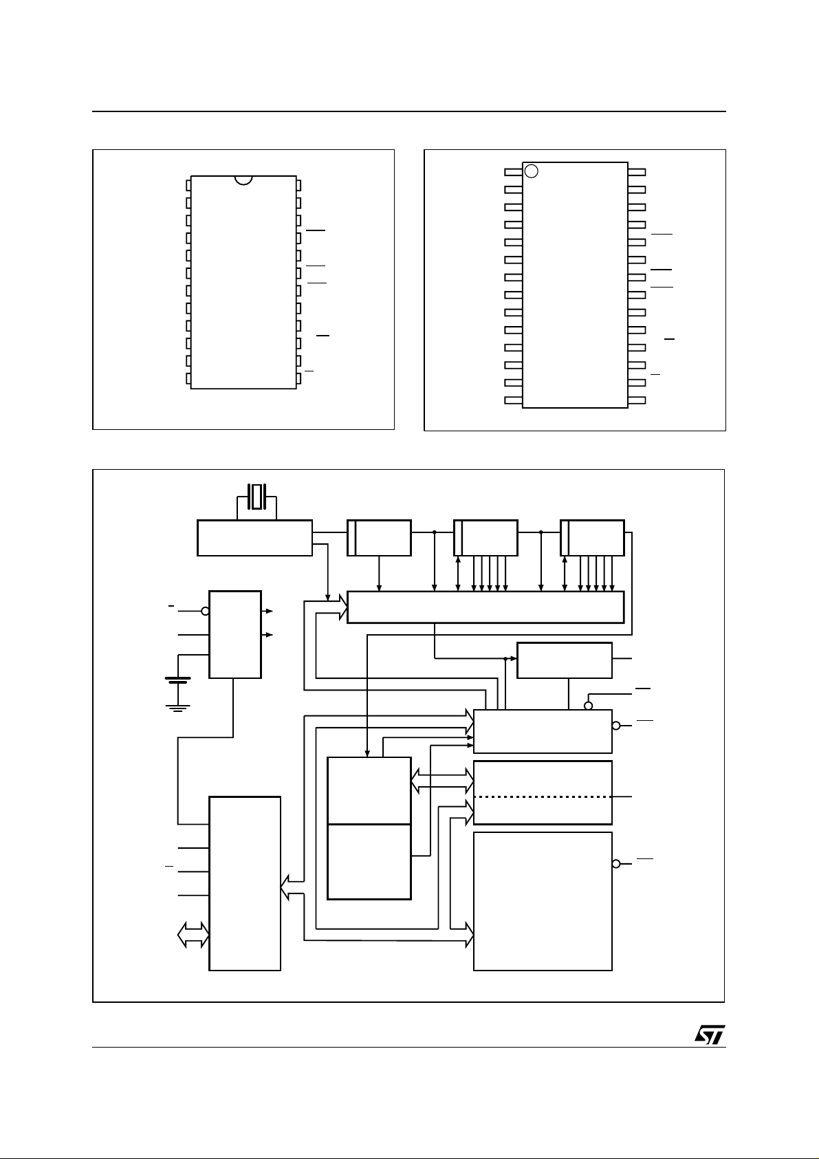
SUMMARY DESCRIPTIO N
The M48T86 is an industry standard Real Time
Clock (RTC). The M48T86 is com posed of a lithium energy source, quartz crystal, write protection
circuitry, and a 128-byte RAM array. This provides
the user with a complete subsystem packaged in
either a 24-pin DIP CAPHAT™ or 28-pin
SNAPHAT
®
SOIC. Functions available to the user
include a non-volatile time-of-day clock, alarm interrupts, a one-hundred-year clock with programmable interrupts, square wave output, and 128
bytes of non-volatile static RAM.
The 24-pin, 600mil DIP CAPHAT houses the
M48T86 silicon with a quartz crystal and a long-life
lithium button cell in a single package.
The 28-pin, 330mil SOIC provides sockets with
gold plated contacts at bot h ends for direct connection to a separate SNAPHAT
®
housing con-
Figure 3. Logic Diagram Table 1. Signal Names
V
CC
taining the battery and crystal. The unique design
allows the SNAPHAT battery package to be
mounted on top of the SOIC package after the
completion of the surface mount process.
Insertion of the SNAPHAT housing after reflow
prevents potential battery and crystal damage due
to the high temperatures required for device surface-mounting. The SNAPHAT ho using is keyed
to prevent reverse insertion.
The SOIC and battery packages are shipped separately in plastic anti-static tubes or in Tape & Reel
form.
For the 28-lead SOIC, the battery/crystal package
part number is “M4T28-BR12SH” (see Table
20., page 27).
AD0-AD7 Multiplexed Address/Data Bus
E
Chip Enable Input
M48T86
AD0-AD7
R/W
DS
AS
RST
RCL
MOT
8
E
M48T86
V
SS
SQW
IRQ
AI01640
R/W
DS Data Strobe Input
AS Address Strobe Input
RST
RCL
MOT Bus Type Select Input
SQW Square Wave Output
IRQ
V
CC
V
SS
NC Not Connected Internally
WRITE Enable Input
Reset Input
RAM Clear Input
Interrupt Request Output
(Open Drain)
Supply Voltage
Ground
5/29
Page 6
M48T86
Figure 4. 24-pi n D I P Connections Figure 5. 28-pi n S O I C C onnections
1
MOT V
2
NC
3
NC
4
AD0
5
AD1
6
AD2
AD3
AD4
AD5
AD6
7
8
9
10
M48T86
11
12 13
V
SS
Figure 6. Block Diagram
24
23
22
21
20
19
18
17
16
15
14
AI01641
CC
SQW
NC
RCL
NC
IRQ
RST
DS
NC
R/W
ASAD7
E
1
MOT V
NC
NC
AD0
AD1
AD2
AD3
AD4
AD5
AD6
2
3
4
5
6
7
8
9
10
11
M48T86
12
V
SS
V
SS
13
14
28
27
26
25
24
23
22
21
20
19
18
17
16
15
AI01642
NCNC
CC
SQW
NC
RCL
NC
IRQ
RST
DS
NC
R/W
ASAD7
E
NC
V
CC
V
BAT
DS
R/W
AS
AD0-AD7
OSCILLATOR
E
POWER
SWITCH
AND
WRITE
PROTECT
BUS
INTERFACE
V
CC
POK
/ 8 / 64 / 64
PERIODIC INTERRUPT/SQUARE WAVE SELECTOR
SQUARE WAVE
OUTPUT
REGISTERS A,B,C,D
CLOCK/
CALENDAR
UPDATE
BCD/BINARY
INCREMENT
CLOCK CALENDAR,
AND ALARM RAM
STORAGE
REGISTERS
(114 BYTES)
SQW
IRQ
RST
DOUBLE
BUFFERED
RCL
6/29
AI01643
Page 7

OPERATION
Automatic deselection of the device ensures the
CC
fall
CC
to sta-
data integrity is not compromised s hould V
below specified Power-fail Deselect Voltage
) levels (see Figure 16., page 22). The auto-
(V
PFD
matic deselection of the device remains in effect
upon power up for a period of 200ms (max ) after
rises above V
V
CC
, provided that the Real
PFD
Time Clock is running and the count-down chain is
not reset. This allows sufficient time for V
bilize and gives the s ystem clock a wake-up period
so that a valid system rese t can be established.
The block diagram in Figure 6., page 6 shows the
pin connections and the major internal functions of
the M48T86.
Signal Description
, VSS. DC power is provided to the device on
V
CC
these pins.The M48T86 uses a 5V V
CC
.
SQW (Square Wave Output). During normal operation (e.g., valid V
), the SQW pin can output a
CC
signal from one of 13 taps. The freque ncy of the
SQW pin can be changed by programming Register A as shown in Table 4., page 14. The SQW signal can be turned on a nd off using the SQWE Bit
(Register B; Bit 3). The SQW signal is not available when V
is less than V
CC
PFD
.
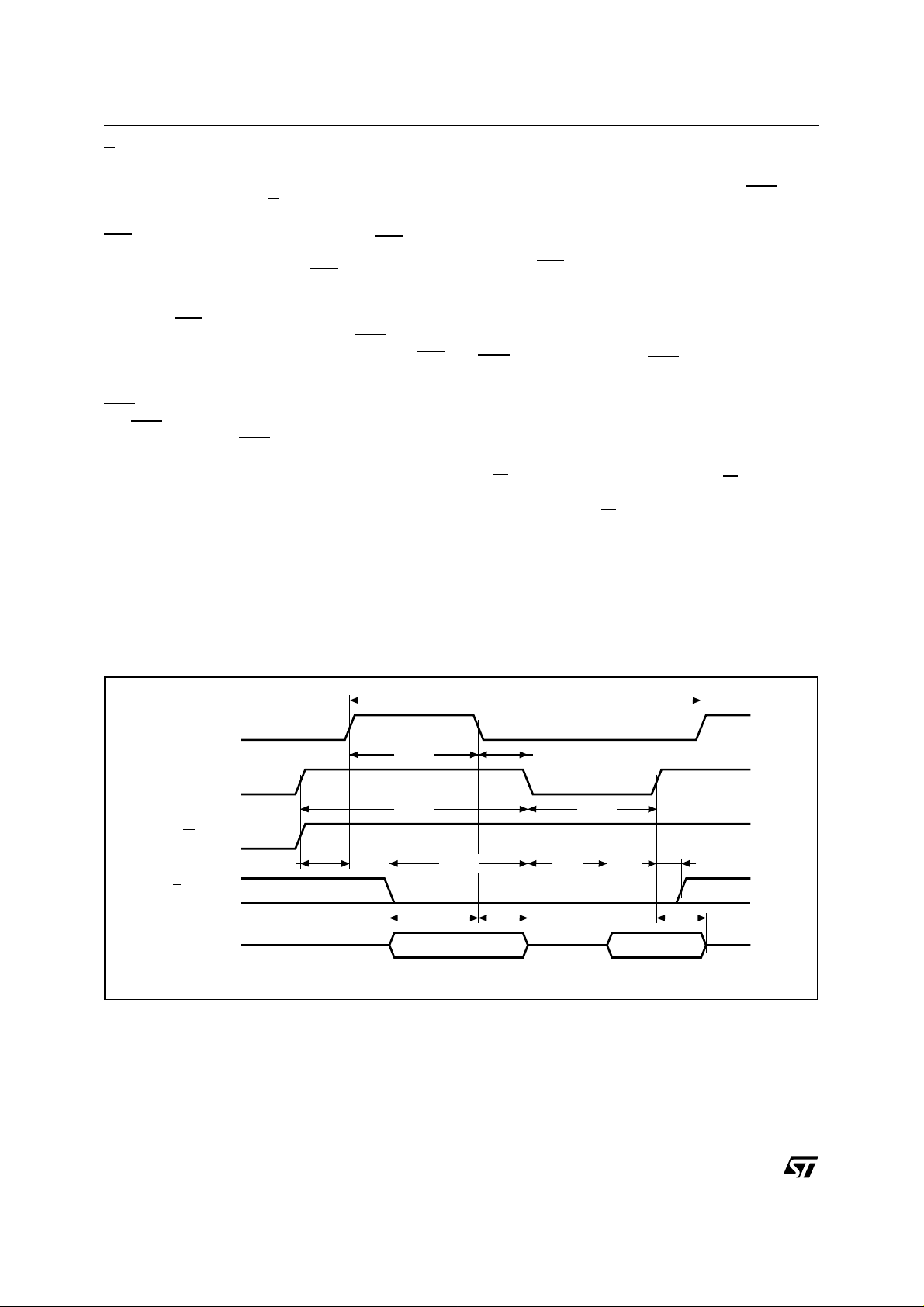
AD0-AD7 (Multiplexed Bi-Directional Address/ Data Bus). The M48T86 provides a multiplexed
bus in which address an d data information s hare
the same signal path. The bus cycle consists of
two stages; first the address is latched, followed by
the data. Address/Data multiplexing does not slow
M48T86
the access time of the M48T86, because the bus
change from address to data occurs during the internal RAM access time. Addre sses must be valid
prior to the falling edge of AS (see Figure
7., page 8), at which time the M48T86 la tches the
address present on AD 0-AD7. Valid W RITE data
must be present and held stable during the l atter
portion of the R/W
a READ cycle, the M4 8T86 output s 8 bits of data
during the latter portion of the DS pulse. The
READ cycle is terminated and the bus returns to a
high impedance state upon a high transition on R/
.
W AS (Address Strobe Inpu t). A positive going
pulse on the Address Strobe (AS) input serves to
demultiplex the bus. The falling edge of AS causes
the address present on AD0-AD7 to be latched
within the M48T86.
MOT (Mode Select). The MOT pin offers the flexibility to choose between two bus types (s ee Fig-
ure 9., page 9). When connected to V
bus timing is selected. When conne cted to V
left disconnected, Intel bus timing is selected. The
pin has an internal pull-down resistance of approximately 20KΩ.
DS (Data Strobe Input). The DS pin is also referred to as READ (RD). A f alling edge transition on the Data Strobe (DS) inpu t enables the ou tput during a a READ cycle. This is very similar to an Output Enable (G es.
pulse (see Figure 8., page 9). In
, Motorola
CC
SS
or
) signal on other memory devic-
7/29
Page 8
M48T86
E (Chip Enable Input). The Chip Enable pin
must be asserted low for a bus cycle in the
M48T86 to be accessed. Bus cycles which take
place without asserting E
will latch the addresses
present, but no data access will occur.
(Interrupt Request Output) . The IRQ pin is
IRQ
an open drain output that can be used as an interrupt input to a processor. The IRQ
output remains
low as long as the status bi t causing the i nterrupt
is present and the corresponding interrupt-enable
bit is set. IRQ
whenever Register C is read. The RST
returns to a high impedance state
pin can
also be used to clear pending interrupts. The IRQ
bus is an open drain output so it requires an external pull-up resistor to V
RST
(Reset Input). The M48T86 is reset when
the R ST
input is p ulled low. Wit h a vali d VCC ap-
plied and a low on RST
.
CC
, the following event s oc-
cur:
1. Periodic Interrupt Enable (PIE) Bit is cleared to
a zero (Register B; Bit 6);
2. Alarm Interrupt Enable (AIE) Bit is cleared to a
zero (Register B; Bit 5);
3. Update Ended Interrupt Request (UF) Bit is
cleared to a zero (Register C; Bit 4);
4. Interrupt Request (IRQF) Bit is cleared to a
zero (Register C Bit 7);
5. Periodic Interrupt Flag (PF) Bit is cleared to a
zero (Register C; Bit 6);
6. The device is not accessible until RST
is re-
turned high;
7. Alarm Interrupt Flag (AF) Bit is cleared to a
zero (Register C; Bit 5);
8. The IRQ
pin is in the high impedance state
9. Square Wave Output Enable (SQWE) Bit is
cleared to zero (Register B; Bit 3); and
10. Update Ended Interrupt Enable (UIE) is
cleared to a zero (Register B; Bit 4).
(RAM Clear). The RCL pin is used to c lear
RCL
all 114 storage bytes, excluding clock and control
registers, of the array to FF (hex) value. T he array
will be cleared when the RCL
pin is held low for at
least 100ms with the osc illator running. Usage of
this pin does not affect battery load. This function
is applicable only when V
(READ/WRITE Input). T he R/W pin is us ed
R/W
is applie d.
CC
to latch data into the M 48T86 and provides f unctionality si mi lar to W
in other memory systems.
Non-Volatile RAM
The 114 general-purpose non-volatile RAM bytes
are not dedicated to any special function within the
M48T86. They can be used by t he proces sor program as non-volatile me mory a nd are fully accessible during the update cycle.
Figure 7. Intel Bus READ AC Waveform
AS
DS
R/W
tDAS tCS tOD tCH
E
AD0-AD7
tCYC
tASDtASW
tDSL tDSH
tAS tAH tDHR
AI01647
8/29
Page 9
Figu r e 8 . Intel Bus WRIT E Mode AC Waveform
AS
M48T86
tCYC
tDAS
DS
tDSL tDSH
R/W
tCS
E
tAS tAH
AD0-AD7
Figure 9. Motorola Bus READ/WRITE Mode AC Waveforms
AS
tDAS
DS
tASDtASW
tCYC
tASDtASW
tCH
tDW
tDHW
AI01648
R/W
E
AD0-AD7
(Write)
AD0-AD7
(Read)
tDSL
tRWS
tCS
tAH
tAS tDHW
tAS tOD
tAH
tDSH
tRWH
tCH
tDW
tDHR
AI01649
9/29
Page 10

M48T86
Table 2. AC Characteristics
Symbol
t
CYC
t
DSL
t
DSH
t
RWH
t
RWS
t
CS
t
CH
t
DHR
t
DHW
t
AS
t
AH
t
DAS
t
ASW
t
ASD
t
OD
t
DW
t
BUC
(2)
t
PI
t
UC
Note: 1. Valid for Ambient Op erating Temp erature: TA = 0 to 70°C; VCC = 4.5 to 5.5V (except where noted).
2. See Table 4., page 14.
Cycle Time 160 ns
Pulse Width, Data Strobe Low or R/W High 80 ns
Pulse Width, Data Strobe High or R/W Low 55 ns
R/W Hold Time 0 ns
R/W Setup Time 10 ns
Chip Select Setup Time 5 ns
Chip Select Hold Time 0 ns
READ Data Hold Time 0 25 ns
WRITE Data Hold Time 0 ns
Address Setup Time 20 ns
Address Hold Time 5 ns
Delay Time, Data Strobe to Address Strobe Rise 10 ns
Pulse Width Address Strobe High 30 ns
Delay Time, Address Strobe to Data Strobe Rise 35 ns
Output Data Delay Time from Data Strobe Rise 50 ns
WRITE Setup Time 30 ns
Delay Time before Update Cycle 244 µs
Periodic Interrupt Time interval – – –
Time of Update Cycle 1 µs
Parameter
(1)
Min Typ Max
M48T86
Unit
10/29
Page 11

CLOCK OPERATIONS
Address Map
The address map of the M48T86 is shown in Figure 10. It consists of 114 bytes of user RAM, 10
bytes of RAM that contain the RTC time, calendar
and alarm data, and 4 bytes which are used for
control and status. All bytes can be read or written
to except for the following:
1. Registers C & D are “Read only.”
2. Bit 7 of Register A is “Read only.”
The contents of the four Registers A, B, C, and D
are described in the “Registers” section.
Time, Calendar, and Ala rm Locations
The time and calendar information is obtained by
reading the appropriate memory bytes. Th e time,
calendar, and alarm regist ers are set or initialized
by writing the appropriate RAM bytes. The contents of the time, calendar, and alarm bytes can be
either Binary or Binary-Coded Decimal (BCD) format. Before writing the internal time, calendar, and
alarm register, the SET Bit (Register B; Bit 7)
should be written to a logic '1.' This will prevent updates from occurring while access is being attempted. In addition to writing the time, calenda r,
and alarm registers in a selected format (binary or
BCD), the Data Mode (DM) Bit (Register B; Bit 2),
must be set to the appropriate logic level ('1' signi-
M48T86
fies binary data; '0' signifies Binary Coded Decimal
(BCD data). All time, calendar, and alarm bytes
must use the same data mode. The SET Bit
should be cleared after the Data Mode Bit has
been written to allow the Real Time Clock to update the time and calendar bytes. Once initialized,
the Real Time Clock makes all updates in the selected mode. The da ta mode cann ot be changed
without reinitializing the ten data bytes. Table
3., page 12 shows the bi nary and BCD formats of
the time, calendar, and alarm locations. The 24/12
Bit (Register B; Bit 1) cannot be changed without
reinitializing the hour locations. When the 12-hour
format is selected, a logic '1' in the high order bit of
the hours byte represents PM. The time, calendar,
and alarm bytes are always acc essible because
they are double-buffered. Once per second the ten
bytes are advanced by one second and checked
for an alarm condition. If a READ of the time and
calendar data occurs during an update, a problem
exists where data such as seconds, minutes, or
hours may not correlate. However, the probability
of reading incorrect time and calendar data is low.
Methods of avoiding possible incorrect time and
calendar READs are reviewed later in this text.
Figure 10. Address Map
0
14
BYTES
114
BYTES
127
CLOCK AND CONTROL
STATUS REGISTERS
13
14
STORAGE REGISTERS
00
0D
0E
7F
0
1
SECONDS ALARM
2
3
MINUTES ALARM
4
5
6
7
DATE OF MONTH
8
9
10
11
12
13
SECONDS
MINUTES
HOURS
HOURS ALARM
DAY OF WEEK
MONTH
YEAR
REGISTER A
REGISTER B
REGISTER C
REGISTER D
BCD OR
BINARY
FORMAT
AI01650
11/29
Page 12

M48T86
Table 3. Time, Calendar, and Alarm Formats
Address RTC Bytes
Decimal Binary BCD
0 Seconds 0-59 00-3B 00-59
1 Seconds Alarm 0-59 00-3B 00-59
2 Minutes 0-59 00-3B 00-59
3 Minutes Alarm 0-59 00-3B 00-59
Hours, 12-hrs 1-12
4
Hours, 24-hrs 0-23 00-17 00-23
Range
01-0C AM
81-8C PM
01-12 AM
81-92 PM
5
Hours Alarm, 12-hrs 1-12
Hours Alarm, 24-hrs 0-23 00-17 00-23
6 Day of Week (1 = Sun) 1-7 01-07 01-07
7 Day of Month 1-31 01-1F 01-31
8 Month 1-12 01-0C 01-12
9 Year 0-99 00-63 00-99
01-0C AM
81-8C PM
Interrupts
The RTC plus RAM includes three separate, fully
automatic sources of interrupt (alarm, periodic, update-in-progress) available to a processor. The
alarm interrupt can be programmed to occur at
rates from once per second t o once per d ay. The
periodic interrupt can be selected from rates of
500ms to 122µ s. The update-ended interrupt c an
be used to indicate that an update cycle has completed.
The processor program can select which interrupts, if any, are going to be used. Th ree bits in
Register B enable the interrupts. Writing a logic '1'
to an interrupt-enable bit (Register B; Bit 6 = PI E;
Bit 5 = AIE; Bit 4 = UIE) permits an interrupt to be
initialized when the event occurs. A '0' in an interrupt-enable bit prohibits the IRQ
pin from being asserted from that interrupt con dition. If an i nterrupt
flag is already set when an interrupt is enabled,
is immediately set at an active level, although
IRQ
the interrupt initiating the event may have occurred
much earlier. As a result, there are cases where
the program should clear such earlier initiated interrupts before first enabling new interrupts.
When an interrupt event occurs, the related flag bi t
(Register C; Bit 6 = PF; Bit 5 = AF; Bit 4 = UF) is
set to a logic '1.' These flag bits are set ind ependent of the state of the corresponding enable bit in
Register B and can be used in a polling mode without enabling the correspon ding enable bits. The
interrupt flag bits are status bits which software
can interrogate as necessary.
When a flag is set, an in dication is given to software that an interrupt event has occurred since the
flag bit was last read; however, care should be taken when using the flag bits as all are cleared each
time Register C is read. Double la tchin g is i ncluded with Register C so that bits which are set remain stable throughout the READ cycle. All bits
which are set high are cleared when read. Any
new interrupts which are pending during the READ
cycle are held until after the cycle is completed.
One, two, or three bits can be set when reading
Register C. Each utilized flag b it should be examined when read to ensure that no interrupts are
lost.
The second flag bit usage method is with fu lly enabled interrupts. When an interrupt flag bit is set
and the corresponding enable bit is also set, the
pin is asserted low. IRQ is asserted as long as
IRQ
at least one of the three interrupt sources has its
flag and enable bits both set. The IR QF Bit (Register C; Bit 7) is a '1' whenever the IRQ
driven low. Determination that the RTC ini tiated an
interrupt is accomplished by reading Register C. A
logic '1' in the IRQF Bit indicates that one or more
interrupts have been initiated by the M48T86. The
act of reading Register C clears all active flag bits
and the IRQF Bit.
01-12 AM
81-92 PM
pin is being
12/29
Page 13

Periodic Inte rrup t
The periodic interrupt will cause the IRQ
pin to go
to an active state from once every 500ms to once
every 122µs. This function is separate from the
alarm interrupt which can be output from once per
second to once per day. The periodic interrupt rate
is selected using the same Reg ister A bits which
select the square wave frequency (see Table
4., page 14). Changing the Register A bits affects
both the square wave frequency and the periodic
interrupt output. However, each function has a
separate enable bit in Register B. The periodic interrupt is enabled by the PIE Bit (Register B; Bit 6).
The periodic interrupt can be used with software
counters to measure inputs, create output intervals, or await the next needed software function.
Alarm Interrupt
The alarm interrupt provides the system processor
with an interrupt when a match is made between
the RTC's hours, minutes, and seconds bytes and
the corresponding alarm bytes.
The three alarm bytes can be used in two ways.
First, when the alarm time is written in the appropriate hours, minutes, and seconds alarm locations, the alarm interrupt is initiated at the specified
time each day if the Alarm Interrupt Enable Bit
(Register B; Bit 5) is high. The second use is to insert a “Don't care” state in one or more of the three
alarm bytes. The “Don't care” code is any hexadecimal value from C0 to FF. The two most significant bits of each byte set the “Don't care”
condition when at logic '1.' An alarm will be generated each hour when the “Don't c are” is are set in
the hours byte. Similarly, an alarm is generated
every minute with “Don't care” codes in the hour
and minute alarm bytes. The “Don't care” codes in
all three alarm bytes create an interrupt every second.
Update Cycle Interrupt
After each update cycle, the Updat e Cycle Ended
Flag Bit (UF) (Register C; Bit 4) is set to a '1.' If the
Update Interrupt Enable Bit (UIE) (Register B; Bit
4) is set to a '1,' and the SET Bit (Register B; Bit 7)
is a '0,' then an interrupt request is ge nerated at
the end of each update cycle.
Oscillator Control Bits
When the M48T86 is shipped f rom the f actory the
internal oscillator is turned off. This feature prevents the lithium energy cell from being discharged until it is installed in a system. A pattern of
M48T86
“010” in Bits 4-6 of Register A will turn the oscillator
on and enable the countdow n chain. A pattern of
“11X” will turn the oscillator on, but holds the
countdown chain of the oscillator in reset. All other
combinations of Bits 4-6 keep the oscillator off.
Update Cycle
The M48T86 executes an up date cycle once per
second regardless of the SET Bit (Reg ister B; Bit
7). When the SET Bit is asserted, the user copy of
the double buffered time, calendar, and alarm
bytes is frozen and will not update as the time increments. However, the time countdown chain
continues to update the internal copy of the buffer.
This feature allows accurate time to be maintained, independent of reading and writing the
time, calendar, and alarm buffers. This also guarantees that the time and calendar in formation will
be consistent. The update cycle also compares
each alarm byte with the corresponding time byte
and issues an alarm if a m atch or if a “Don't c are”
code is present in all three positions.
There are three methods of accessing the real
time clo ck tha t wil l avo id a ny po ssib ilit y of obta ining inconsistent time and calendar data. The first
method uses the update-ended interrupt. If enabled, an interrupt occurs after every update cycle
which indicates that over 999ms are available to
read valid time and date information. If this interrupt is used, the IRQF Bit (Register C; Bit 7) should
be cleared before leaving the interrupt routine.
A second method uses the Update-In-Progress
(UIP) Bit (Register A; Bit 7) to determine if the update cycle is in progress. The UIP Bit will pulse
once per second. After the UIP Bit goes high, the
update transfer occurs 244µs later. If a low is read
on the UIP Bit, the user has at least 244µs before
the time/calendar data will be changed. Therefore,
the user should avoid interrupt service routines
that would cause the time needed to read valid
time/calendar data to exceed 244µs.
The third method uses a periodic interrupt to determine if an update cycle is in progress. The UIP Bit
is set high between the setting of the PF Bit (Register C; Bit 6). Periodic interrupts that occur at a
rate greater than t
formation to be reached at each occurrence of the
periodic interrupt.The READs should be completed within 1/(t
PL/2
read during the update cycle.
allow valid time and date in-
BUC
+ t
) to ensure that data is not
BUC
13/29
Page 14

M48T86
Square Wave Output Selec tion
Thirteen of the 15 divider taps are made available
to a 1-of-15 selector, as sho wn in the block diagram of Figure 6., page 6. The purpose of selecting a divider tap is to generate a square wave
output signal on the SQW pin. The RS3-RS0 bits
in Register A establish the square wave output frequency. These frequencies are listed in Table
Table 4. Square Wave Frequency/Pe riodi c Interrup t Ra te
Register A Bits Square Wave Periodic Interrupt
RS3 RS2 RS1 RS0 Frequency Units Period Units
0000None None
0 0 0 1 256 Hz 3.90625 ms
0 0 1 0 128 Hz 7.8125 ms
0 0 1 1 8.192 kHz 122.070 us
0 1 0 0 4.096 kHz 244.141 us
0 1 0 1 2.048 kHz 488.281 us
0 1 1 0 1.024 kHz 976.5625 us
4., page 14. The SQW frequency selection shares
the 1-of-15 selector with the periodic interrupt generator. Once the frequency is selecte d, the ou tput
of the SQW pin can be turned on and off under
program control with the Square Wave Enabled
(SQWE) Bit.
0 1 1 1 512 Hz 1.953125 ms
1 0 0 0 256 Hz 3.90625 ms
1 0 0 1 128 Hz 7.8125 ms
1 0 1 0 64 Hz 15.625 ms
1 0 1 1 32 Hz 31.25 ms
1 1 0 0 16 Hz 62.5 ms
11018Hz125ms
11104Hz250ms
11112Hz500ms
14/29
Page 15
Register A
UIP. Update in Progress. The Update in
Progress (UIP) Bit is a status flag that can be monitored. When the UIP Bit is '1,' the update transfer
will soon occur (see Figure 11). When UIP is a '0,'
the update transfer will not occur for at least
244µs. The time, calendar, and alarm information
in RAM is fully availa ble for acce ss whe n the U IP
Bit is '0.' The UIP Bit is “Read only” and is not a ffected by RST
. Writing the SET Bit in Register B to
a '1' inhibits any update transfer and clears the UIP
Status Bit.
OSC0, OSC1, OSC2. Oscillator Control. These
three bits are used to control the oscillator and reset the countdown chain. A pattern of “010” enables operation by turning on the oscillator and
enabling the divider chain. A pattern of 11X turns
the oscillator on, but keeps t he frequency d ivider
disabled. When “010” is written, the first update
begins after 500ms.
RS3, RS2, RS1, RS0. These four rate-selection
bits select one of the 1 3 taps on the 15-stage divider or disable the divider output. The tap sel ected may be used to generate an output square
wave (SQW pin) and/or a periodic interrupt. The
user may do one of the following:
1. Enable the interrupt with the PIE Bit;
or
2. Enable the SQW output with the SQWE Bit;
or
3. Enable both at the same time and same rate;
or
4. Enable neither.
Table 4., p age 14 lists the periodic interrupt rates
and the square wave frequencies that may be chosen with the RS Bits. These four READ/WRITE
bits are not affected by RST
.
Table 5. REGISTER A MSB
BIT7 BIT6 BIT5 BIT4 BIT3 BIT2 BIT1 BIT0
UIP OSC2 OSC1 OSC0 RS3 RS2 RS1 RS0
M48T86
Figure 11. Upd a te Pe rio d Ti m in g and UIP
UIP
UPDATE PERIOD (1sec)
tBUC tUC
AI01651
15/29
Page 16

M48T86
Register B
SET. When the SE T Bit i s a '0, ' the update trans-
fer functions normally by advancing the counts
once per second. When the SET Bit is written to a
'1,' any update transfer is inhibited and the program may initialize the time and calendar bytes
without an update occurring. READ cycles can be
executed in a similar manner. SET is a READ/
WRITE bit which is not modified by RST
functions of the M48T86.
PIE: Perio dic Interrupt Enable. The Periodic Interrupt Enable Bit (PIE) is a READ/WRITE bit
which allows the Periodic Interrupt Flag (PF) Bit in
Register C to cause the IRQ
pin to be driven low
(see Figure 12., page 17 for the relationship be-
tween PIE and UIE). When the PIE Bit is set to '1,'
periodic interrupts are generated by driving the
pin low at a rate specified by the RS3-RS0
IRQ
bits of Register A. A '0' in the PIE Bit blocks the
output from being driven by a periodic inter-
IRQ
rupt, but the Periodic Flag (PF) Bit is still set at the
periodic rate. PIE is not modified by any internal
M48T86 functions, but is cleared to '0' on RST
AIE: Alarm Interrupt Enable. The Alarm Interrupt Enable (AIE) Bit is a READ/WRITE bit which,
when set to a '1,' permits the Alarm Flag (AF) Bit in
Register C to assert IRQ
. An alarm interrupt occurs for each second that the three time bytes
equal the three alarm bytes including a “Don't
care” alarm code of binary 1XXXXXXX. When the
AIE Bit is set to '0,' the AF Bit does not initiate the
signal. The RST pin clears AIE to '0.' The in-
IRQ
ternal functions of the M48T86 do not affect the
AIE Bit.
or internal
.
UIE: Update Ended Interrupt Enable. The Update Ended Interrupt Enable (UIE) Bit is a READ/
WRITE bit which enables the Update End Flag
(UF) Bit in Register C to assert IRQ
low on the RST
pin or the SET Bit going high
. A trans ition
clears the UIE Bit.
SQWE: Square Wave Enable. When the Square
Wave Enable (SQWE) Bit is s et to a '1,' a square
wave signal is driven out on the SQW pin. The frequency is determined by the rate-selection bits
RS3-RS0. When the SQWE Bit is set to '0,' the
SQW pin is held low. The SQWE Bit is cleared by
the RST
pin. SQWE is a READ/WRITE bit.
DM: Data Mode. The Data Mode (DM) Bit indicates whether time and calendar information are in
binary or BCD format. The DM Bit is set by the program to the appropriate format and can be read as
required. This bit is not modified by internal function or RST
. A '1' in DM signifies binary data and a
'0' specifies Binary Coded Decimal (BCD) data.
24/12
The 24/12 Control Bit establishes the format of the
hours byte. A '1' indicates the 24-hour mode and a
'0' indicates the 12-hour m ode. This bit is RE AD/
WRITE and is not affected by internal functions or
.
RST
DSE. Daylight Savings Enable
The Daylight Savings Enable (DSE) Bit is a READ/
WRITE bit which enables two special updates
when set to a '1.' On the first Sunda y in April, the
time increments from 1:59:59AM to 3:00:00 A M.
On the last Sunday in October, when the time
reaches 1:59:59 AM, it changes to 1:00:00 AM.
These special updates do not occur when the DSE
Bit is a '0.' This bit is not affected by internal functions or RST
.
Table 6. REGISTER B MSB
BIT7 BIT6 BIT5 BIT4 BIT3 BIT2 BIT1 BIT0
SET PIE AIE UIE SQWE DM 24/12 DSE
16/29
Page 17

Figure 12. Update-ended/Periodic Interrupt Relationship
UPDATE PERIOD (1sec)
UIP
M48T86
PF
UF
tPI
tPI tPI
tBUC tUC
AI01652B
17/29
Page 18

M48T86
Register C
IRQF: Interrupt Request Flag. The Interrupt Re-
quest Flag (IRQF) Bit is s et to a '1' when one or
more of the following are true:
PF = PIE = 1
AF = AIE = 1
UF = UIE = 1
(e.g., IRQF = PF*PIE+AF*AIE+UF*UIE)
PF: Periodic Interrupt Flag. The Periodic Inter-
rupt Flag (PF) is a “Read only” bit which is set to a
'1' when an edge is detected on the selected tap of
the divider chain. The RS3-RS0 bits establish the
periodic rate. PF is set to a '1' independent of the
state of the PIE Bit. Th e IRQ
will set th e IRQF Bit. Th e PF Bit is clea red by a
or a software READ of Register C.
RST
AF: Alarm Flag. A '1 ' in the AF (Alarm Interrupt
Flag) Bit indicates that the current time has
matched the alarm time. If the AIE Bit is also a '1,'
the I RQ
IRQF Bit. A RST
pin will go low and a '1' will appear in the
or a READ of Register C will clear
AF.
signal is active and
UF: Update Ended Interrupt Flag. The Update
Ended Interrupt Flag (UF) Bit is set after each update cycle. When the UIE Bit is set to a '1,' the '1'
in the UF Bit causes the IRQF Bit to be a '1.' This
will assert t he IRQ
Register C or a RST
pin. UF is cleared by reading
.
BIT 0 throug h 3: Unused Bits. Bit 3 through Bit
0 are unused. These bits always read '0' and cannot be written.
Register D
VRT: Valid Ram A nd Time. T he Valid RAM and
Time (VRT) Bit is set to the '1' s tate by STMicroelectronics prior to shipment. This bit is not writable and should always be a '1' when read. If a '0'
is ever present, an exhausted internal lithium cell
is indicated and both the contents of the RTC data
and RAM data are questionable. This bit is unaffected by RST
.
BIT 0 throug h 6: Unused Bits. The remaining
bits of Register D are not usable. They cannot be
written and when read, they will always read '0.'
Table 7. REGISTER C MSB
BIT7 BIT6 BIT5 BIT4 BIT3 BIT2 BIT1 BIT0
IRQFPFAFUF0000
Table 8. REGISTER D MSB
BIT7 BIT6 BIT5 BIT4 BIT3 BIT2 BIT1 BIT0
VRT0000000
18/29
Page 19

M48T86
VCC Noise And Negative Going Transients
transients, including those produced by output
I
CC
switching, can produce voltage fluctuations, resulting in spikes on the V
bus. These transients
CC
can be reduced if capacitors are used to store energy which stabilizes the V
bus. The energy
CC
stored in the bypass capacitors will be released as
low going spikes are generated or energy will be
absorbed when overshoots occur. A ceramic bypass capacitor value of 0.1µF (as shown in Figure
13) is recommended in order to provide the need-
ed filtering.
In addition to transients that are caused by normal
SRAM operation, power cycling can generate negative voltage spikes on V
below V
by as much as one volt. These negative
SS
that drive it to values
CC
spikes can cause data corruption in the SRAM
while in battery backup mode. To protect from
these voltage spikes, it is recommended to connect a schottky diode from V
connected to V
, anode to VSS). Schottky diode
CC
to VSS (cathode
CC
1N5817 is recommended for through hole and
MBRS120T3 is recommended for surface mount.
Figure 13. Supply Voltage Protection
V
CC
V
CC
0.1µF DEVICE
V
SS
AI02169
19/29
Page 20

M48T86
MAXIMUM RA T ING
Stressing the device above the rating listed in the
“Absolute Maximum Ratings” table may cause
permanent damage to the device. These are
stress ratings only and operation of the device at
these or any other conditions above those indicated in the Operating sections of this specification is
Table 9. Absolute Maximum Ratings
Symbol Parameter Value Unit
T
A
T
STG
(1,2,3)
T
SLD
V
IO
V
CC
P
D
Note: 1. For DIP package: Soldering temperature not to exceed 260°C for 10 seconds (total thermal budget not to exceed 150°C for longer
than 30 seconds).
2. For S O package, standard (SnPb) lead finish: Reflow at peak t em perature of 225°C (tota l thermal budg et not to exceed 180°C for
between 90 to 15 0 s e c o nds).
3. For S O package , Lead-free (Pb-free) lead finish: Reflow at peak tempera tu re of 260°C (total thermal budget not to exceed 245°C
for greater than 30 seconds).
CAUTION: Nega tive undershoot s below –0.3V are not allowed on any pin whil e i n the Battery Ba ck -up mode.
CAUTION: Do NOT wave s ol d er SOIC to av oid damag i n g S NA PHAT socket s.
Ambient Operating Temperature 0 to 70 °C
Storage Temperature (VCC Off, Oscillator Off)
Lead Solder Temperature for 10 seconds 260 °C
Input or Output Voltages –0.3 to 7.0 V
Supply Voltage –0.3 to 7.0 V
Power Dissipation 1 W
not implied. Exposure to Absol ute Max imum Ra ting conditions for extended periods may affect device reliability. Refer also to the
STMicroelectronics SURE Program and other relevant quality documents.
–40 to 85 °C
20/29
Page 21
DC AND AC PARAMETERS
This section summarizes the operating and measurement conditions, as well as the DC and AC
characteristics of the device. The parameters in
the following DC and AC Characteristic tables are
derived from tests performed under the Meas ure-
Table 10. Operating and AC Measurement Conditions
Parameter M48T86 Unit
ment Conditions listed in t he relevant tables. Designers should check that the operating conditions
in their projects match the measurement conditions when using the quoted parameters.
M48T86
Supply Voltage (V
Ambient Operating Temperature (T
Load Capacitance (C
CC
)
)
A
)
L
4.5 to 5.5 V
0 to 70 °C
100 pF
Input Rise and Fall Times ≤ 5ns
Input Pulse Voltages 0 to 3 V
Input and Output Timing Ref. Voltages 1.5 V
Note: O utput Hi-Z is def i ned as the poin t where data is no l onger driven.
Figure 14. AC Te st i ng Load Circuit (No IRQ ) Figure 15. AC Testing Load Circuit (with IRQ)
FOR ALL
OUTPUTS
EXCEPT IRQ
510Ω
5V
960Ω
IRQ
50pF
5V
1.15kΩ
130pF
AI01644
Table 11. Capacitance
Symbol
C
IN
C
IO
Note: 1. Effec tive capacitance measured with powe r supply at 5V; sam pl ed only, not 100% tested.
2. At 25°C, f = 1MHz.
3. Outputs deselect ed.
Input Capacitance 7 pF
(3)
Input / Output Capacitance 5 pF
Parameter
(1,2)
Min Max Unit
AI01645
21/29
Page 22

M48T86
Table 12. DC Characteristics
IN
≤ V
≤ V
CC
CC
(1)
Min Max Unit
2.4 V
Symbol Parameter
I
LI
I
LO
I
CC
V
V
Input Leakage Current
(2)
Output Leakage Current
Supply Current Outputs open 15 mA
Input Low Voltage –0.3 0.8 V
IL
Input High Voltage 2.2
IH
Output Low Voltage
V
OL
V
OH
Note: 1. Valid for Ambient Op erating Temp erature: TA = 0 to 70°C; VCC = 4.5 to 5.5V (except where noted).
2. Outputs deselect ed.
Output Low Voltage (IRQ
Output High Voltage
)
Test Condition
0V ≤ V
0V ≤ V
OUT
= 4mA
I
OL
= 0.5mA
I
OL
I
= –1mA
OH
Figure 16. Power Down/Up Mode AC Waveforms
V
CC
4.5V
V
PFD
VSO
±1 µA
±1 µA
V
+ 0.3
CC
0.4 V
0.4 V
V
tF tR
E
Table 13. Power Down/Up Mode AC Characteristics
Symbol
(2)
t
F
t
R
t
rec
Note: 1. Valid for Ambient Op erating Temp erature: TA = 0 to 70°C; VCC = 4.5 to 5.5V (except where noted).
2. V
VCC Fall Time
VCC Rise Time
V
to E High
PFD
fall time of less than tF may res ul t in desel e c tion/w ri te prot ection no t occurr i n g until 200µs after VCC passes V
CC
Parameter
(1)
Min Max Unit
300 µs
100 µs
20 200 ms
Table 14. Power Down/Up Trip Points DC Characteristics
Symbol
V
PFD
V
SO
(3)
t
DR
Note: 1. Valid for Ambient Op erating Temp erature: TA = 0 to 70°C; VCC = 4.5 to 5.5V (except where noted).
2. All voltages referenced to V
3. At 25°C, V
Power-fail Deselect Voltage 4.0 4.35 V
Battery Back-up Switchover Voltage 3.0 V
Expected Data Retention Time 10 YEARS
= 0V.
CC
Parameter
.
SS
(1,2)
Min Typ Max Unit
trec
AI01646
PFD
.
22/29
Page 23

PACKAG E MECHANICA L INFORMATION
Figure 17. PCDIP24 – 24-pin Plastic DIP, battery CAPHAT, Package Outline
A2
M48T86
B1 B
A1AL
e1
C
eA
e3
D
N
E
1
Note: D rawing is not to scale.
PCDIP
Table 15. PCDIP24 – 24-pin Plastic DIP, battery CAPHAT, Package Mechanical Data
Symb
Typ Min Max Typ Min Max
A 8.89 9.65 0.3500 0.3799
A1 0.38 0.76 0.0150 0.0299
A2 8.36 8.89 0.3291 0.3500
B 0.38 053 0.0150 0.0209
mm inches
B1 1.14 1.78 0.0449 0.0701
C 0.20 0.31 0.0079 0.0122
D 34.29 34.80 1.3500 1.3701
E 17.83 18.34 0.7020 0.7220
e1 2.29 2.79 0.0902 0.1098
e3 25.15 30.73 0.9902 1.2098
eA 15.24 16.00 0.6000 0.6299
L 3.05 3.81 0.1201 0.1500
N24 24
23/29
Page 24

M48T86
Figure 18. SOH28 – 28-lead Plastic Small Outline, 4-socket SNAPHAT, Package Outli ne
A2
A
C
Be
eB
CP
D
N
E
H
LA1 α
1
SOH-A
Note: D rawing is not to scale.
Table 16. SOH28 – 28-lead Plastic Small Outline, 4-socket battery SNAPHAT, Pack. Mech. Data
Symb
Typ Min Max Typ Min Max
mm inches
A 3.05 0.1201
A1 0.05 0.36 0.0020 0.0142
A2 2.34 2.69 0.0921 0.1059
B 0.36 0.51 0.0142 0.0201
C 0.15 0.32 0.0059 0.0126
D 17.71 18.49 0.6972 0.7280
E 8.23 8.89 0.3240 0.3500
e1.27– –0.0500– –
eB 3.20 3.61 0.1260 0.1421
H 11.51 12.70 0.4531 0.5000
L 0.41 1.27 0.0161 0.0500
α 0° 8° 0° 8°
N 28 28
CP 0.10 0.0039
24/29
Page 25

Figure 19. SH – 4-pin SNAPHAT Ho u sing for 48mAh Battery & Cr ystal, Package Outline
M48T86
eA
D
A1
A
B
eB
A3
L
E
SH
Note: D rawing is not to scale.
Table 17. SH – 4-pin SNAPHAT Housing for 48mAh Battery & Cry st al, Pack age Mech. Data
Symb
Typ Min Max Typ Min Max
mm inches
A2
A 9.78 0.3850
A1 6.73 7.24 0.2650 0.2850
A2 6.48 6.99 0.2551 0.2752
A3 0.38 0.0150
B 0.46 0.56 0.0181 0.0220
D 21.21 21.84 0.8350 0.8598
E 14.22 14.99 0.5598 0.5902
eA 15.55 15.95 0.6122 0.6280
eB 3.20 3.61 0.1260 0.1421
L 2.03 2.29 0.0799 0.0902
25/29
Page 26

M48T86
Figure 20. SH – 4-pin SNAPHAT Housing for 120mAh Battery & Crystal, Package Outline
eA
D
A1
A
B
eB
A3
L
E
SHTK-A
Note: D rawing is not to scale.
Table 18. SH – 4-pin SNAPHAT Housing for 120mAh Battery & Crystal, Package Mech. Data
Symb
Typ Min Max Typ Min Max
mm inches
A2
A 10.54 0.415
A1 8.00 8.51 0.315 .0335
A2 7.24 8.00 0.285 0.315
A3 0.38 0.015
B 0.46 0.56 0.018 0.022
D 21.21 21.84 0.835 0.860
E 17.27 18.03 0.680 .0710
eA 15.55 15.95 0.612 0.628
eB 3.20 3.61 0.126 0.142
L 2.03 2.29 0.080 0.090
26/29
Page 27

M48T86
PART NUMBERING
Table 19. Ordering Information Scheme
Example: M48T 86 MH 1 E
Device Type
M48T
Supply Voltage and Write Protect Voltage
86 = V
Package
PC = PCDIP24
MH
Temperature Rang e
1 = 0 to 70°C
= 4.5 to 5.5V; V
CC
(1)
= SOH28
= 4.2 to 4.5V
PFD
Shipping Method
For SOH28:
blank = Tubes (Not for New Design - Use E)
E = Lead-free Package (ECO PACK
F = Lead-free Package (ECO PACK
®
), Tubes
®
), Tape & Reel
TR = Tape & Reel (Not for New Design - Use F)
For PCDIP28:
blank = Tubes
Note: 1. The SOI C package (SOH28) requires the S NA P HAT® battery/cry stal package which is ordered separately unde r the part number
“M4T28- BR 12SH” in plasti c tube or “M4T28-BR12SH T R” in Tape & Reel form (see Tabl e 20).
Caution: Do not place the SNAPHAT battery package “M4TXX-BR12SH” in conductive foam as it will drain the lithium button-cell battery.
For other options, or for more information on any aspect of this device, please contact the ST Sales Office
nearest you.
Table 20. SNAPHAT Battery Table
Part Number Description Package
M4T28-BR12SH Lithium Battery (48mAh) SNAPHAT SH
M4T32-BR12SH Lithium Battery (120mAh) SNAPHAT SH
27/29
Page 28

M48T86
REVISION HISTORY
Table 21. Document Revision History
Date Rev. # Revision Details
March 1999 1.0 First Issue
04-May-00 1.1 Page layou t changed
31-Jul-01 2.0 Reformatted; temp/voltage info. added to tables (Table 12, 2, 13, 14)
20-May-02 2.1 Modify reflow time and temperature footnotes (Table 9)
01-Apr-03 3.0 v2.2 template applied; test condition updated (Table 14)
02-Apr-04 4.0 Reformatted; update Lead-free package information (Table 9, 19)
28/29
Page 29

M48T86
Information furnished is believed to be accurate and reliable. However, STMicroelectronics a ssumes no responsibility fo r the c onsequences
of use of such information nor for any infringement of patents or other rights of third parties which may result from its use. No license is granted
by implication or otherwise under any patent or patent rights of STMicroelectronics. Specifications mentioned in this publication are subject
to change without notice. This publication supersedes and replaces all information previously supplied. STMicroelectronics products are not
authori zed for use as criti cal component s in life support devices or sys tems without ex press written approval of STMicroelect ronics.
The ST logo is a registered trademark of STMi croelectronics.
All other na m es are the property of their respective ow ners.
© 2004 STMi croelectroni cs - All rights reserved
Australi a - B elgium - Braz i l - Canada - China - Czech Republ i c - Finland - France - Germany -
Hong Kong - India - Israel - It al y - Japan - Malays i a - Malta - Morocco - Singapor e -
STMicroelectroni cs GROUP OF COMPANIES
Spain - Sweden - Switzerland - United Kingdom - United States
www.st.com
29/29
 Loading...