

STMicroelectronics M48T58, M48T58Y User Manual
5.0V, 64 Kbit (8 Kb x8) TIMEKEEPER® SRAM
FEAT URES SUMMARY
■ INTEGRATED, ULT RA LOW POWER SRAM,
REAL TIME CLOCK, POWER-FAIL
CONTROL CIRCUIT AND BATTERY
■ BYTEWIDE™ RAM-LIKE CLOCK ACCESS
■ BCD CODED YEAR, MONTH, DAY, DATE,
HOURS, MINUTES, AND SECONDS
■ FREQUENCY TEST OUTPUT FOR REAL
TIME CLOCK
■ AUTOMATIC POWER-FAIL CHIP
DESELECT AND WRITE PROTECT ION
■ WRITE PROTECT VOLTAGES
= Power-fail Deselect Voltage):
(V
PFD
– M48T58: V
4.5V ≤ V
– M48T58Y: V
4.2V ≤ V
■ SELF-CONTAINED BATTERY and
CRYSTAL IN THE CAPHAT™ DIP
PACKAGE
■ PACKAGING INCLUDES A 28-LEAD SOIC
AND SNAPHAT
separately)
■ SOIC PACKAGE PROVIDES DIRECT
CONNECTION FOR A SNAPHAT HOUSING
CONTAINING THE BATTERY AND
CRYSTAL
■ PIN AND FUNCTION COMPATIBLE WITH
JEDEC STANDARD 8 Kb x8 SRAMs
= 4.75 to 5.5V
CC
≤ 4.75V
PFD
= 4.5 to 5.5V
CC
≤ 4.5V
PFD
®
TOP (to be ordered
M48T58
M48T58Y
Figure 1. 28-pin PCDIP, CAPHAT™ Package
28
1
PCDIP28 (PC)
Battery/Crystal
CAPHAT
Figure 2. 28-pi n S O I C Package
SNAPHAT (SH)
Battery/Crystal
28
1
SOH28 (MH)
1/27April 2004

M48T58, M48T58Y
TABLE OF CONTENTS
FEATURES SUMMARY . . . . . . . . . . . . . . . . . . . . . . . . . . . . . . . . . . . . . . . . . . . . . . . . . . . . . . . . . . . . . 1
Figure 1. 28-pin PCDIP, CAPHAT™ Package . . . . . . . . . . . . . . . . . . . . . . . . . . . . . . . . . . . . . . . . . 1
Figure 2. 28-pin SOIC Package . . . . . . . . . . . . . . . . . . . . . . . . . . . . . . . . . . . . . . . . . . . . . . . . . . . . 1
SUMMARY DESCRIPTION. . . . . . . . . . . . . . . . . . . . . . . . . . . . . . . . . . . . . . . . . . . . . . . . . . . . . . . . . . . 4
Figure 3. Logic Diagram . . . . . . . . . . . . . . . . . . . . . . . . . . . . . . . . . . . . . . . . . . . . . . . . . . . . . . . . . . 4
Table 1. Signal Names . . . . . . . . . . . . . . . . . . . . . . . . . . . . . . . . . . . . . . . . . . . . . . . . . . . . . . . . . . 4
Figure 4. DIP Connections . . . . . . . . . . . . . . . . . . . . . . . . . . . . . . . . . . . . . . . . . . . . . . . . . . . . . . . . 5
Figure 5. SOIC Connections. . . . . . . . . . . . . . . . . . . . . . . . . . . . . . . . . . . . . . . . . . . . . . . . . . . . . . . 5
Figure 6. Block Diagram . . . . . . . . . . . . . . . . . . . . . . . . . . . . . . . . . . . . . . . . . . . . . . . . . . . . . . . . . . 5
OPERATION MODES . . . . . . . . . . . . . . . . . . . . . . . . . . . . . . . . . . . . . . . . . . . . . . . . . . . . . . . . . . . . . . . 6
Table 2. Operating Modes. . . . . . . . . . . . . . . . . . . . . . . . . . . . . . . . . . . . . . . . . . . . . . . . . . . . . . . . 6
READ Mode . . . . . . . . . . . . . . . . . . . . . . . . . . . . . . . . . . . . . . . . . . . . . . . . . . . . . . . . . . . . . . . . . . . 7
Figure 7. READ Mode AC Waveforms . . . . . . . . . . . . . . . . . . . . . . . . . . . . . . . . . . . . . . . . . . . . . . . 7
Table 3. RE A D Mode AC Charac teristics . . . . . . . . . . . . . . . . . . . . . . . . . . . . . . . . . . . . . . . . . . . . 8
WRITE Mode. . . . . . . . . . . . . . . . . . . . . . . . . . . . . . . . . . . . . . . . . . . . . . . . . . . . . . . . . . . . . . . . . . . 9
Figure 8. WRITE Enable Controlled, WRITE AC Waveform. . . . . . . . . . . . . . . . . . . . . . . . . . . . . . . 9
Figure 9. Chip Enable Controlled, WRITE AC Waveforms. . . . . . . . . . . . . . . . . . . . . . . . . . . . . . . 10
Table 4. WRITE Mode AC Characteristics . . . . . . . . . . . . . . . . . . . . . . . . . . . . . . . . . . . . . . . . . . 11
Data Retention Mode. . . . . . . . . . . . . . . . . . . . . . . . . . . . . . . . . . . . . . . . . . . . . . . . . . . . . . . . . . . 12
CLOCK OPERATIONS . . . . . . . . . . . . . . . . . . . . . . . . . . . . . . . . . . . . . . . . . . . . . . . . . . . . . . . . . . . . . 13
Reading the Clock. . . . . . . . . . . . . . . . . . . . . . . . . . . . . . . . . . . . . . . . . . . . . . . . . . . . . . . . . . . . . 13
Setting the Clock. . . . . . . . . . . . . . . . . . . . . . . . . . . . . . . . . . . . . . . . . . . . . . . . . . . . . . . . . . . . . . 13
Stopping and Starting the Oscillator. . . . . . . . . . . . . . . . . . . . . . . . . . . . . . . . . . . . . . . . . . . . . . 13
Table 5. Register Map . . . . . . . . . . . . . . . . . . . . . . . . . . . . . . . . . . . . . . . . . . . . . . . . . . . . . . . . . . 13
Calibrating the Clock. . . . . . . . . . . . . . . . . . . . . . . . . . . . . . . . . . . . . . . . . . . . . . . . . . . . . . . . . . . 14
Figure 10.Crystal Accuracy Across Temperature . . . . . . . . . . . . . . . . . . . . . . . . . . . . . . . . . . . . . . 15
Figure 11.Clock Calibration. . . . . . . . . . . . . . . . . . . . . . . . . . . . . . . . . . . . . . . . . . . . . . . . . . . . . . . 15
Battery Low Flag . . . . . . . . . . . . . . . . . . . . . . . . . . . . . . . . . . . . . . . . . . . . . . . . . . . . . . . . . . . . . . 16
Century Bit. . . . . . . . . . . . . . . . . . . . . . . . . . . . . . . . . . . . . . . . . . . . . . . . . . . . . . . . . . . . . . . . . . . 16
V
Noise And Negative Going Transients. . . . . . . . . . . . . . . . . . . . . . . . . . . . . . . . . . . . . . . . . 16
CC
Figure 12.Supply Voltage Protection. . . . . . . . . . . . . . . . . . . . . . . . . . . . . . . . . . . . . . . . . . . . . . . . 16
MAXIMUM RATING. . . . . . . . . . . . . . . . . . . . . . . . . . . . . . . . . . . . . . . . . . . . . . . . . . . . . . . . . . . . . . . . 17
Table 6. Absolute Maximum Ratings. . . . . . . . . . . . . . . . . . . . . . . . . . . . . . . . . . . . . . . . . . . . . . . 17
DC AND AC PARAMETERS. . . . . . . . . . . . . . . . . . . . . . . . . . . . . . . . . . . . . . . . . . . . . . . . . . . . . . . . . 18
Table 7. Operating and AC Measurement Conditions. . . . . . . . . . . . . . . . . . . . . . . . . . . . . . . . . . 18
Figure 13.AC Measurement Load Circuit . . . . . . . . . . . . . . . . . . . . . . . . . . . . . . . . . . . . . . . . . . . . 18
Table 8. Capacitance . . . . . . . . . . . . . . . . . . . . . . . . . . . . . . . . . . . . . . . . . . . . . . . . . . . . . . . . . . . 1 8
Table 9. DC Characteristics. . . . . . . . . . . . . . . . . . . . . . . . . . . . . . . . . . . . . . . . . . . . . . . . . . . . . . 19
2/27

M48T58, M48T58Y
Figure 14.Power Down/Up Mode AC Waveforms. . . . . . . . . . . . . . . . . . . . . . . . . . . . . . . . . . . . . . 20
Table 10.Power Down/Up AC Characteristics . . . . . . . . . . . . . . . . . . . . . . . . . . . . . . . . . . . . . . . . 20
Table 11.Power Down/Up Trip Points DC Characteristics . . . . . . . . . . . . . . . . . . . . . . . . . . . . . . . 20
PACKAGE MECHANICAL INFORMATION . . . . . . . . . . . . . . . . . . . . . . . . . . . . . . . . . . . . . . . . . . . . . 21
Figure 15.PCDIP28 – 28-pin Plastic DIP, battery CAPHAT, Package Outline . . . . . . . . . . . . . . . . 21
Table 12. PCDIP28 – 28-pin Plastic DIP, battery CAPHAT, Package Mechanical Data. . . . . . . . . 21
Figure 16.SOH28 – 28-lead Plastic Small Outline, 4-socket battery SNAPHAT, Package Outline. 22
Table 13. SOH28 – 28-lead Plastic Small Outline, 4-socket battery SNAPHAT, Pack. Mech. Data22
Figure 17.SH – 4-pin SNAPHAT Housing for 48mAh Battery & Crystal, Package Outline . . . . . . . 23
Table 14. SH – 4-pin SNAPHAT Housing for 48mAh Battery & Crystal, Package Mech. Data. . . . 23
Figure 18.SH – 4-pin SNAPHAT Housing for 120mAh Battery & Crystal, Package Outline . . . . . . 24
Table 15. SH – 4-pin SNAPHAT Housing for 120mAh Battery & Crystal, Package Mech. Data. . . 24
PART NUMBERING . . . . . . . . . . . . . . . . . . . . . . . . . . . . . . . . . . . . . . . . . . . . . . . . . . . . . . . . . . . . . . . 25
Table 16.Ordering Information Scheme . . . . . . . . . . . . . . . . . . . . . . . . . . . . . . . . . . . . . . . . . . . . . 25
Table 17.SNAPHAT Battery Table . . . . . . . . . . . . . . . . . . . . . . . . . . . . . . . . . . . . . . . . . . . . . . . . . 25
REVISION HISTORY. . . . . . . . . . . . . . . . . . . . . . . . . . . . . . . . . . . . . . . . . . . . . . . . . . . . . . . . . . . . . . . 26
Table 18.Document Revision History. . . . . . . . . . . . . . . . . . . . . . . . . . . . . . . . . . . . . . . . . . . . . . . 26
3/27
M48T58, M48T58Y
SUMMARY DESCRIPTIO N
The M48T58/Y TIMEKEEPER® RAM is a 8Kb x 8
non-volatile static RAM and real time clock. The
monolithic chip is available in two special packages to provide a highly integrated battery backed-up
memory and real time clock solution.
The M48T58/Y is a non-volatile pin and function
equivalent to any JEDEC standard 8Kb x 8 SRAM.
It also easily fits into many ROM, EPROM, and
EEPROM sockets, providing the non-volatility of
PROMs without any requirement for special
WRITE timing or limitations on the number of
WRITEs that can be performed.
The 28-pin, 600mil DIP CAPHAT™ houses the
M48T58/Y silicon with a quartz crystal and a long
life lithium button cell in a single package.
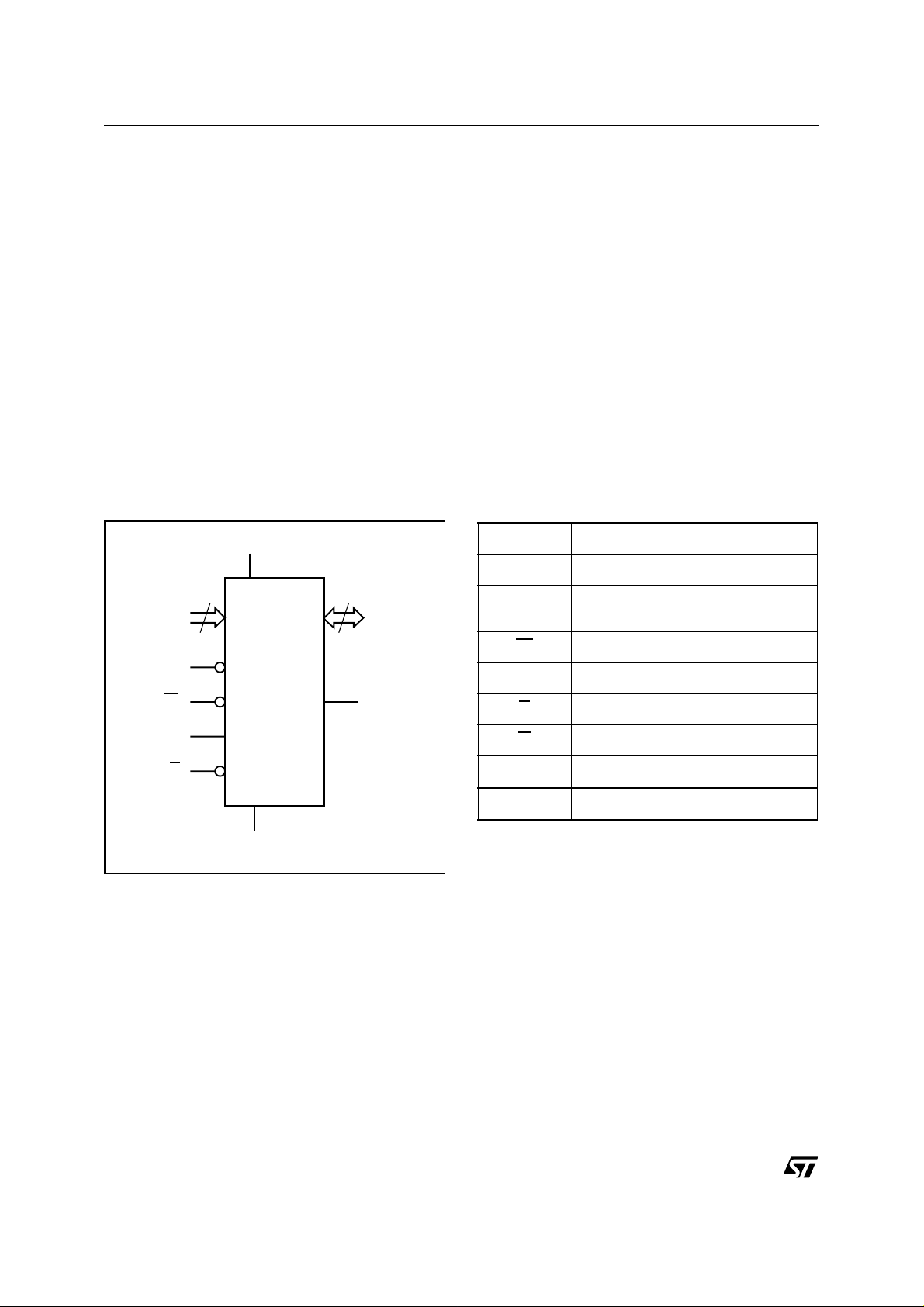
Figure 3. Logic Diagram Table 1. Signal Names
The 28-pin, 330mil SOIC provides sockets with
gold plated contacts at bot h ends for direct connection to a separate SNAPHAT
taining the battery and crystal. The unique design
allows the SNAPHAT battery package to be
mounted on top of the SOIC package after the
completion of the surface mount process. Insertion of the SNAPHAT housing after reflow prevents potential battery and c rystal dam age due to
the high temperatures required for device surfacemounting. The SNAPHAT housing is keyed to prevent reverse insertion. The SOIC and battery/crystal packages are shipped separately in plastic antistatic tubes or in Tape & Reel form.
For the 28-lead SOIC, the battery/crystal package
(e.g., SNAPHAT) part number is “M4T28BR12SH” (see Table 17., page 25).
®
housing con-
V
CC
13
A0-A12
W
E1 FT
E2
G
M48T58
M48T58Y
V
SS
8
DQ0-DQ7
AI01374B
A0-A12 Address Inputs
DQ0-DQ7 Data Inputs / Outputs
FT
E1
E2 Chip Enable 2
G
W
V
CC
V
SS
Frequency Test Output (Open
Drain)
Chip Enable 1
Output Enable
WRITE Enable
Supply Voltage
Ground
4/27
M48T58, M48T58Y
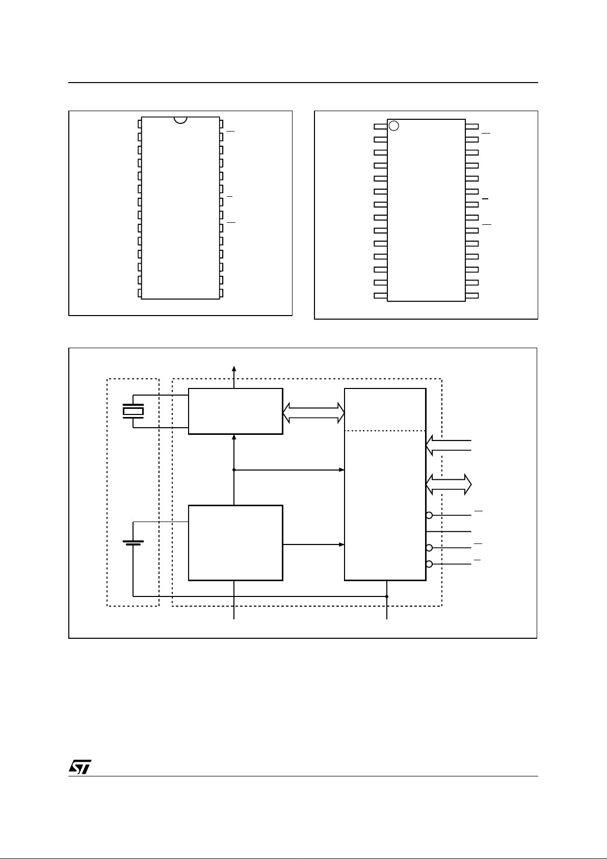
Figure 4. DIP C on ne ctions Figure 5. SOI C Co nn e ct io ns
1
FT V
2
A12
3
A7
4
A6
5
A5
A4
6
A3
7
M48T58
8
A2
A1
A0
DQ0
M48T58Y
9
10
11
12
DQ2
13
14
SS
Figure 6. Block Diagram
28
27
26
25
24
23
22
21
20
19
18
17
16
15
AI01375B
CC
W
E2
A8
A9
A11
G
A10
E1
DQ7
DQ6
DQ5DQ1
DQ4
DQ3V
FT
FT V
A12
A7
A6
A5
A4
A3
A2
A1
A0
DQ0
1
2
3
4
5
6
7
8
9
10
11
M48T58Y
12
DQ2
SS
13
14
AI01376B
28
27
26
25
24
23
22
21
20
19
18
17
16
15
CC
W
E2
A8
A9
A11
G
A10
E1
DQ7
DQ6
DQ5DQ1
DQ4
DQ3V
32,768 Hz
CRYSTAL
LITHIUM
CELL
OSCILLATOR AND
CLOCK CHAIN
VOLTAGE SENSE
AND
SWITCHING
CIRCUITRY
V
CC
POWER
V
PFD
8 x 8 BiPORT
SRAM ARRAY
8184 x 8
SRAM ARRAY
V
SS
A0-A12
DQ0-DQ7
E1
E2
W
G
AI01377C
5/27
M48T58, M48T58Y
OPERATION MODES
As Figure 6., page 5 shows, the static memory array and the quartz controlled clock oscillator of the
M48T58/Y are integr ated on one silicon c hip. T he
two circuits are interconnected at the up per eight
memory locations to provide user accessible
BYTEWIDE™ clock information in t he bytes with
addresses 1FF8h-1FFFh. The clock locations
contain the century, year, month, date, day, hour,
minute, and second in 24 hour BCD format (except
for the century). Corrections for 28, 29 (l eap year valid until 2100), 30, and 31 day months are made
automatically. Byte 1FF8h is the clock control register. This byte controls user access to the clock
information and also stores the clock calibration
setting.
The eight clock bytes are not the actual clock
counters themselves; they are memory locations
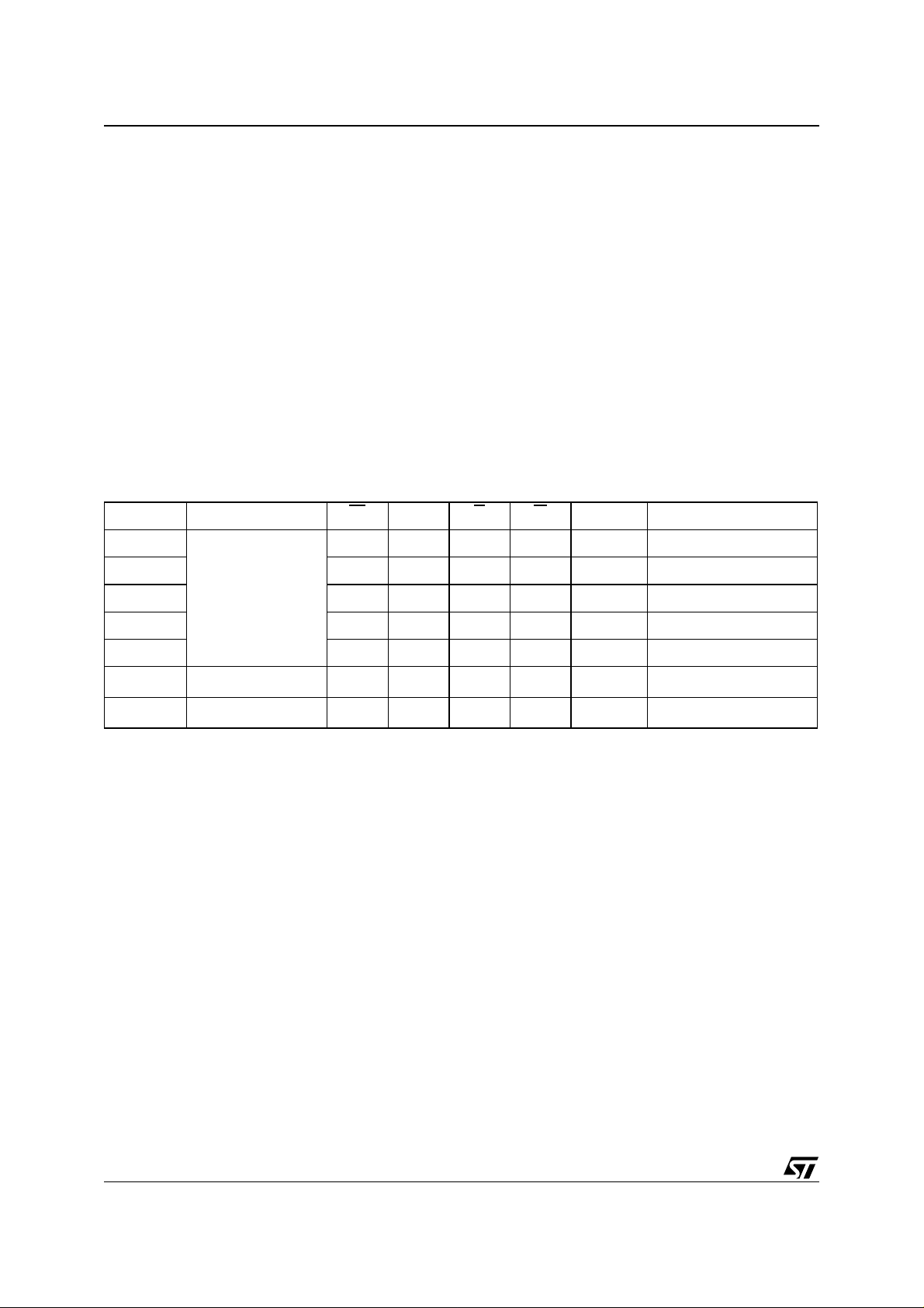
Table 2. Operating Modes
Mode
Deselect
Deselect X
WRITE
READ
READ
Deselect
Deselect
Note: X = VIH or VIL; VSO = Battery B ack-up Switchover Voltage.
1. See Table 11., page 20 for details.
VSO to V
V
CC
4.75 to 5.5V
or
4.5 to 5.5V
(min)
PFD
(1)
≤ V
SO
E1 E2 G W DQ0-DQ7 Power
(1)
V
IH
V
IL
V
IL
V
IL
X X X X High Z CMOS Standby
X X X X High Z Battery Back-up Mode
X X X High Z Standby
V
IL
V
IH
V
IH
V
IH
consisting of BiPORT™ READ/write memory
cells. The M48T58/Y includes a clock control circuit which updates the clock bytes with current information once per second. The information can
be accessed by the user in the same manner as
any other location in the static memory array.
The M48T58/Y also has its own Pow er-fail Detect
circuit. The control circuitry constantly monitors
the single 5V supply for an out-of-tolerance condition. When V
is out of tolerance, the circuit write
CC
protects the SRAM, providing a high degree of
data security in the midst of unpredictable system
operation brought on by low V
. As VCC falls be-
CC
low the Battery Back-up Switchover Voltage
), the control circuitry connects the battery
(V
SO
which maintains data and clock operation until valid power returns.
X X High Z Standby
X
V
IL
V
IH
V
IL
V
IH
V
IH
D
IN
D
OUT
High Z Active
Active
Active
6/27
READ Mode
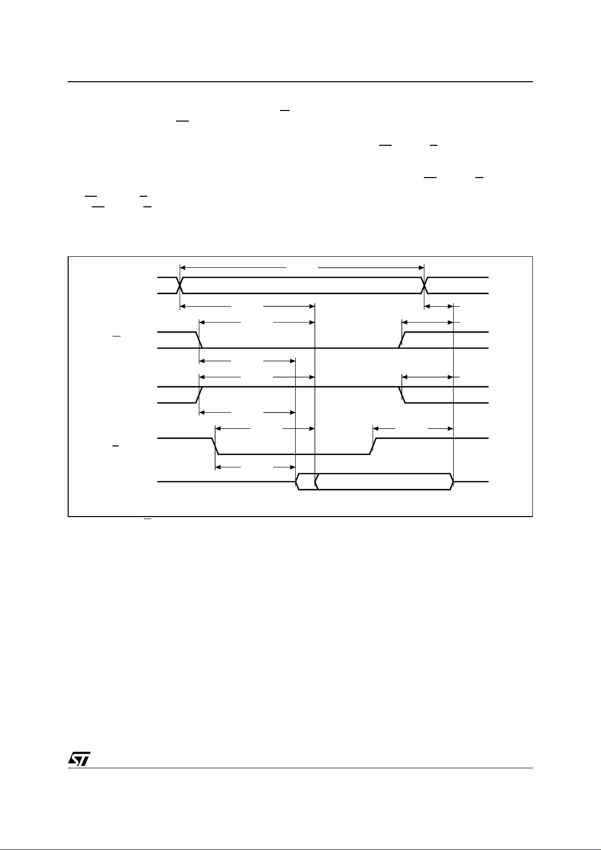
The M48T58/Y is in the READ Mode whenever W
(WRITE Enable) is high, E1 (Chip Enable 1) is low,
and E2 (Chip Enable 2) is high. The unique address specified by the 13 Address Inputs defines
which one of the 8, 192 bytes of d ata is to be accessed. Valid data will be available at the Data I/O
pins within Address Access time (t
AVQV
) after the
last address input signal is stable, providing that
, E2, and G access times are also satis fi e d .
the E1
If the E1
, E2 and G access ti mes are not met , valid
data will be available after the latter of the Chip En-
Figure 7. READ Mode AC Waveforms
M48T58, M48T58Y
able Access times (t
Enable Access time (t
E1LQV
GLQV
or t
).
The state of the eight t hree-state Da ta I/O si gnals
is controlled by E1
tivated before t
an indeterminate state until t
Inputs are changed while E1
, E2 and G. If the outputs are ac-
, the data lines will be driven to
AVQV
AVQV
, E2 and G remain active, output data will remain valid for Output Data
Hold time (t
) but will go indeterminate until the
AXQX
next Address Access.
tAVAV
) or Output
E2HQV
. If the Address
A0-A12
E1
E2
G
DQ0-DQ7
Note: W RITE Enable (W) = High.
VALID
tAVQV tAXQX
tE1LQV
tE1LQX
tE2HQV
tE2HQX
tGLQX
tGLQV
tGHQZ
VALID
tE1HQZ
tE2LQZ
AI00962
7/27
M48T58, M48T58Y
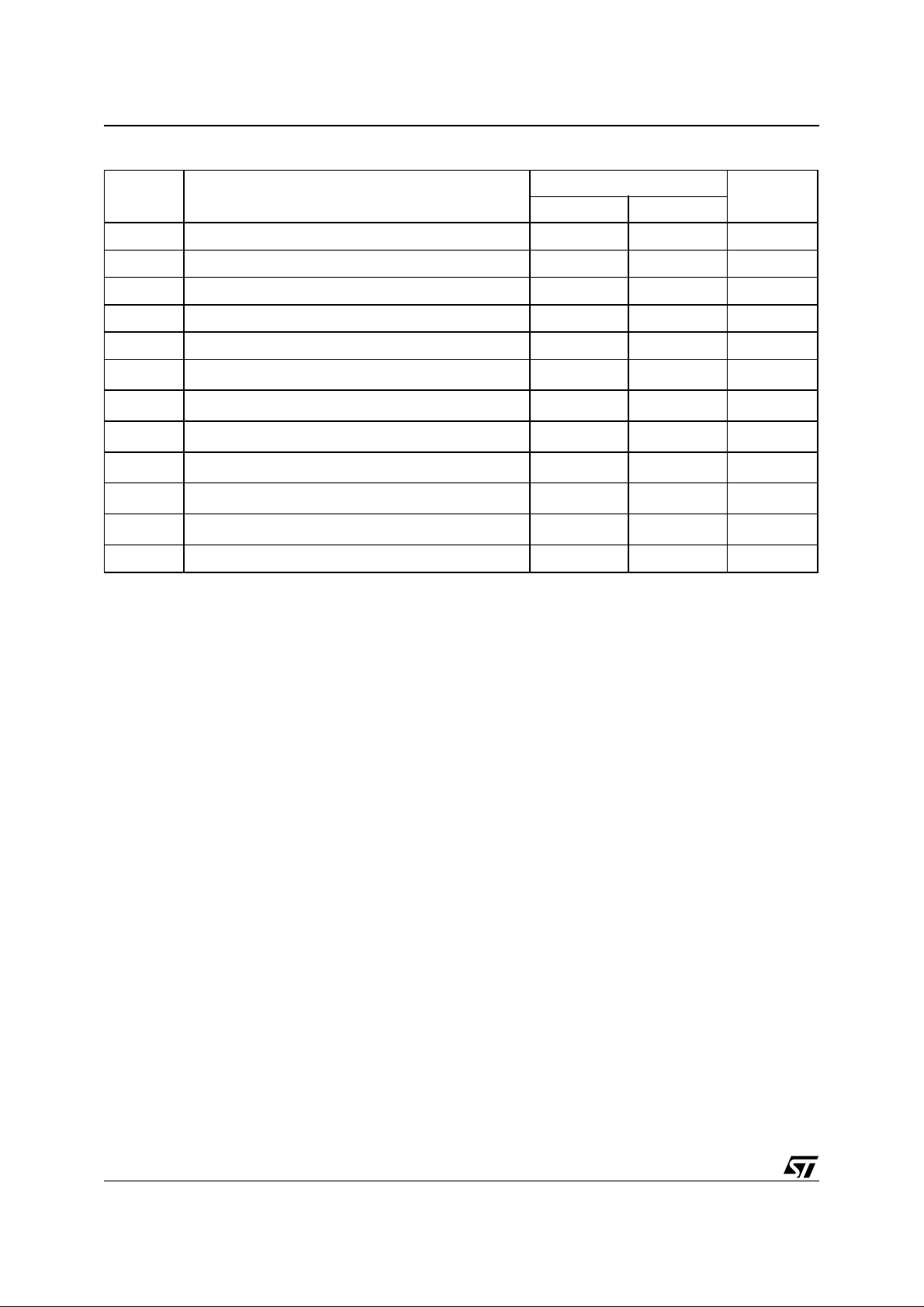
Table 3. READ Mode AC Characteristics
Symbol
t
AVAV
t
AVQV
t
E1LQV
t
E2HQV
t
GLQV
t
E1LQX
t
E2HQX
t
GLQX
t
E1HQZ
t
E2LQZ
t
GHQZ
t
AXQX
Note: 1. Valid for Ambient Op erating Temp erature: TA = 0 to 70°C; VCC = 4.75 to 5.5V or 4.5 to 5.5V (except where noted).
2. C
READ Cycle Time 70 ns
Address Valid to Output Valid 70 ns
Chip Enable 1 Low to Output Valid 70 ns
Chip Enable 2 High to Output Valid 70 ns
Output Enable Low to Output Valid 35 ns
(2)
Chip Enable 1 Low to Output Transition 5 ns
(2)
Chip Enable 2 High to Output Transition 5 ns
(2)
Output Enable Low to Output Transition 5 ns
(2)
Chip Enable 1 High to Output Hi-Z 25 ns
(2)
Chip Enable 2 Low to Output Hi-Z 25 ns
(2)
Output Enable High to Output Hi-Z 25 ns
Address Transition to Output Transition 10 ns
= 5pF.
L
Parameter
(1)
M48T58/Y
Min Max
Unit
8/27
WRITE Mode
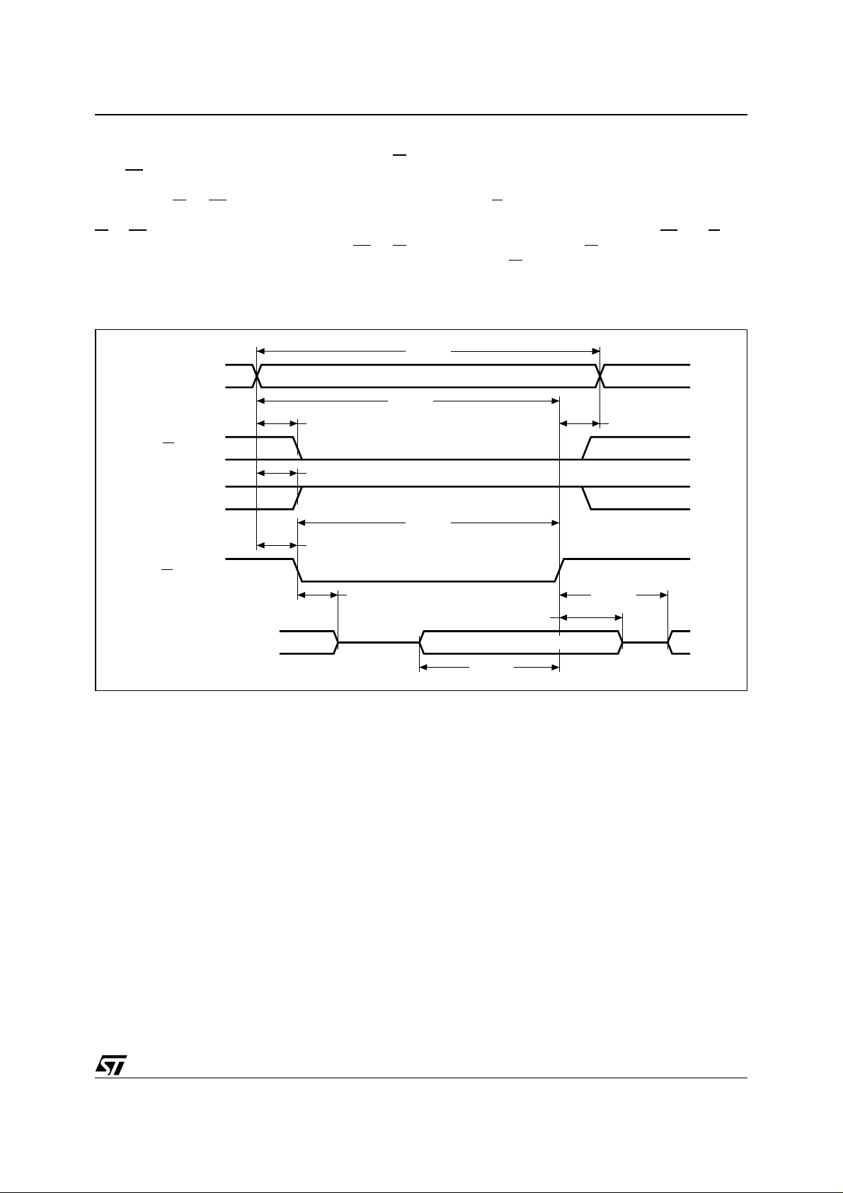
The M48T58/Y is in the WRITE Mode whenever W
and E1 are low and E2 is high. The start of a
WRITE is referenced from the latter occurring falling edge of W
or E1, or the rising edge of E2. A
WRITE is terminated by the earlier rising edge of
or E1, or the falling edge of E 2. The addr ess es
W
must be held valid throughout the cycle. E1
must return high or E2 low for a minimum of t
or t
from Chip Enabl e or t
E2LAX
from WRITE
WHAX
or W
E1HAX
Enable prior to the initiation of another READ or
WRITE cycle. Data -i n must be valid t
the end of WRITE and remain valid for t
terward. G
cles to avoid bus contention; although, if the output
bus has been activated by a low on E1
a high on E2, a low o n W
t
WLQZ
Figure 8. WRITE Enable Controlled, WRITE AC Waveform
tAVAV
M48T58, M48T58Y
DVWH
should be kept high during WRITE cy-
will disable the o utputs
after W falls.
prior to
af-
WHDX
and G and
A0-A12
E1
E2
W
DQ0-DQ7
tAVE1L
tAVE2H
tAVWL
tWLQZ
VALID
tAVWH
tWLWH
tDVWH
tWHAX
tWHQX
tWHDX
DATA INPUT
AI00963
9/27
 Loading...