

Page 1
5.0 OR 3.0V, 512 bit (6 4 x 8) SERIAL
FEATURES SUMMARY
■ 5.0 OR 3.0V OPERATING VO LTA G E
■ SERIAL INTERFACE SU PPO R TS I
(400 KHz)
■ NVRAM SUPERVISOR FOR EXTERNAL
LPSRAM
■ OPTIMIZED FOR MINIMAL INTERCONNECT
TO MCU
■ 2.5 TO 5.5V OSCILLATOR OPERATING
VOLTAGE
■ AUTOMATIC SWITCH-OVER and DESELECT
CIRCUITRY
■ CHOICE OF POWER-FAIL DESELECT
VOLTAGES
– M41ST85Y : V
4.20V ≤ V
– M41ST85W: V
2.55V ≤ V
■ 1.25V REFERENCE (for PFI/PFO)
■ COUNTERS FOR TENTHS/HUNDREDTHS
PFD
PFD
= 4.5 to 5.5V;
CC
≤ 4.50V
= 2.7 to 3.6V;
CC
≤ 2.70V
OF SECONDS, SECONDS, MINUTES,
HOURS, DAY, DATE , MONTH, YEAR, and
CENTURY
■ 44 BYTES OF GENERAL PURPOSE RAM
■ PROGRAMMABLE ALARM and INTE RRUPT
FUNCTION (VALID EVEN DURING BATTERY
BACK-UP MODE)
■ WATCHDOG T IME R
■ MICROPROCESSOR POWER-ON RESET
■ BATTERY LOW FLAG
■ POWER-DOWN TIMESTAMP (HT BIT)
■ ULTRA-LOW BATT ERY SU PPL Y C URRE N T
OF 500nA (MAX)
2
C BUS
M41ST85Y
M41ST85W
RTC and NVRAM SUPERVISOR
■ PACKAGING INCLUD ES A 28-LEAD SOIC and
SNAPHAT
■ SOIC SNAPHAT PACKAGE PROVIDES
DIRECT CONNECTION FOR A SNAPHAT
TOP WHICH CONTAINS THE BATTERY and
CRYSTAL
■ SOIC EMBEDDED CR YSTAL P ACKAG E (M X)
OPTION
Figure 1. 28-pi n S O I C Package
Figure 2. 28-pin (300mil) SOIC Package
®
TOP (to be Ordered Separately)
SNAPHAT (SH)
Battery & Crystal
28
1
SOH28 (MH)
EMBEDDED Cryst al
SOX28 (MX)
Rev. 4.0
1/33May 2003
Page 2

M41ST85Y, M41ST85W
TABLE OF CONTENTS
SUMMARY DESCRIPTION. . . . . . . . . . . . . . . . . . . . . . . . . . . . . . . . . . . . . . . . . . . . . . . . . . . . . . . . . . . 4
Figure 3. Logic Diagram . . . . . . . . . . . . . . . . . . . . . . . . . . . . . . . . . . . . . . . . . . . . . . . . . . . . . . . . . . 5
Table 1. Signal Names . . . . . . . . . . . . . . . . . . . . . . . . . . . . . . . . . . . . . . . . . . . . . . . . . . . . . . . . . . . 5
Figure 4. 28-pin SOIC Connections. . . . . . . . . . . . . . . . . . . . . . . . . . . . . . . . . . . . . . . . . . . . . . . . . . 5
Figure 6. Block Diagram . . . . . . . . . . . . . . . . . . . . . . . . . . . . . . . . . . . . . . . . . . . . . . . . . . . . . . . . . . 6
Figure 7. Hardware Hookup . . . . . . . . . . . . . . . . . . . . . . . . . . . . . . . . . . . . . . . . . . . . . . . . . . . . . . . 7
MAXIMUM RATING. . . . . . . . . . . . . . . . . . . . . . . . . . . . . . . . . . . . . . . . . . . . . . . . . . . . . . . . . . . . . . . . . 7
Table 2. Absolute Maximum Ratings. . . . . . . . . . . . . . . . . . . . . . . . . . . . . . . . . . . . . . . . . . . . . . . . . 7
DC and AC PARAMETERS . . . . . . . . . . . . . . . . . . . . . . . . . . . . . . . . . . . . . . . . . . . . . . . . . . . . . . . . . . 8
Table 3. DC and AC Measurement Conditions . . . . . . . . . . . . . . . . . . . . . . . . . . . . . . . . . . . . . . . . . 8
Figure 8. AC Testing Input/Output Waveforms . . . . . . . . . . . . . . . . . . . . . . . . . . . . . . . . . . . . . . . . . 8
Table 4. Capacitance. . . . . . . . . . . . . . . . . . . . . . . . . . . . . . . . . . . . . . . . . . . . . . . . . . . . . . . . . . . . . 8
Table 5. DC Characteristics. . . . . . . . . . . . . . . . . . . . . . . . . . . . . . . . . . . . . . . . . . . . . . . . . . . . . . . . 9
OPERATING MODES . . . . . . . . . . . . . . . . . . . . . . . . . . . . . . . . . . . . . . . . . . . . . . . . . . . . . . . . . . . . . . 10
2-Wire Bus Characteristics . . . . . . . . . . . . . . . . . . . . . . . . . . . . . . . . . . . . . . . . . . . . . . . . . . . . . . 10
Figure 9. Serial Bus Data Transfer Sequence. . . . . . . . . . . . . . . . . . . . . . . . . . . . . . . . . . . . . . . . .11
Figure 11. WRITE Cycle Timing: RTC & External SRAM Control Signals . . . . . . . . . . . . . . . . . . . 12
Figure 12. Bus Timing Requirements Sequence. . . . . . . . . . . . . . . . . . . . . . . . . . . . . . . . . . . . . . . 12
Table 6. AC Characteristics. . . . . . . . . . . . . . . . . . . . . . . . . . . . . . . . . . . . . . . . . . . . . . . . . . . . . . . 12
READ Mode . . . . . . . . . . . . . . . . . . . . . . . . . . . . . . . . . . . . . . . . . . . . . . . . . . . . . . . . . . . . . . . . . . 13
Figure 13. Slave Address Location . . . . . . . . . . . . . . . . . . . . . . . . . . . . . . . . . . . . . . . . . . . . . . . . . 13
Figure 14. READ Mode Sequence . . . . . . . . . . . . . . . . . . . . . . . . . . . . . . . . . . . . . . . . . . . . . . . . . 13
Figure 15. Alternate READ Mode Sequence. . . . . . . . . . . . . . . . . . . . . . . . . . . . . . . . . . . . . . . . . . 14
WRITE Mode. . . . . . . . . . . . . . . . . . . . . . . . . . . . . . . . . . . . . . . . . . . . . . . . . . . . . . . . . . . . . . . . . . 14
Figure 16. WRITE Mode Sequence . . . . . . . . . . . . . . . . . . . . . . . . . . . . . . . . . . . . . . . . . . . . . . . . . 14
Data Retention Mode. . . . . . . . . . . . . . . . . . . . . . . . . . . . . . . . . . . . . . . . . . . . . . . . . . . . . . . . . . . 15
Figure 17. Power Down/Up Mode AC Waveforms . . . . . . . . . . . . . . . . . . . . . . . . . . . . . . . . . . . . . 16
Table 7. Power Down/Up AC Characteristics . . . . . . . . . . . . . . . . . . . . . . . . . . . . . . . . . . . . . . . . . 16
CLOCK OPERATION . . . . . . . . . . . . . . . . . . . . . . . . . . . . . . . . . . . . . . . . . . . . . . . . . . . . . . . . . . . . . . 17
TIMEKEEPER® Registers. . . . . . . . . . . . . . . . . . . . . . . . . . . . . . . . . . . . . . . . . . . . . . . . . . . . . . . 17
Table 8. TIMEKEEPER® Register Map . . . . . . . . . . . . . . . . . . . . . . . . . . . . . . . . . . . . . . . . . . . . . 18
Calibrating the Clock. . . . . . . . . . . . . . . . . . . . . . . . . . . . . . . . . . . . . . . . . . . . . . . . . . . . . . . . . . . 1 9
Setting Alarm Clock Registers. . . . . . . . . . . . . . . . . . . . . . . . . . . . . . . . . . . . . . . . . . . . . . . . . . . 19
Figure 18. Alarm Interrupt Reset Waveform . . . . . . . . . . . . . . . . . . . . . . . . . . . . . . . . . . . . . . . . . . 20
Table 9. Alarm Repeat Modes. . . . . . . . . . . . . . . . . . . . . . . . . . . . . . . . . . . . . . . . . . . . . . . . . . . . . 20
Figure 19. Back-Up Mode Alarm Waveform . . . . . . . . . . . . . . . . . . . . . . . . . . . . . . . . . . . . . . . . . . 21
2/33
Page 3

M41ST85Y, M41ST85W
Watchdog Timer . . . . . . . . . . . . . . . . . . . . . . . . . . . . . . . . . . . . . . . . . . . . . . . . . . . . . . . . . . . . . . 21
Square Wave Outp ut . . . . . . . . . . . . . . . . . . . . . . . . . . . . . . . . . . . . . . . . . . . . . . . . . . . . . . . . . . . 22
Table 10. Square Wave Output Frequency . . . . . . . . . . . . . . . . . . . . . . . . . . . . . . . . . . . . . . . . . . . 22
Power-on Reset . . . . . . . . . . . . . . . . . . . . . . . . . . . . . . . . . . . . . . . . . . . . . . . . . . . . . . . . . . . . . . . 23
Reset Inputs (RSTIN1 & RSTIN2) . . . . . . . . . . . . . . . . . . . . . . . . . . . . . . . . . . . . . . . . . . . . . . . . . 23
Figure 20. RSTIN1 & RSTIN2 Timing Waveforms . . . . . . . . . . . . . . . . . . . . . . . . . . . . . . . . . . . . . 23
Table 11. Reset AC Characteristics . . . . . . . . . . . . . . . . . . . . . . . . . . . . . . . . . . . . . . . . . . . . . . . . 2 3
Power-fail INPUT/OUTPUT . . . . . . . . . . . . . . . . . . . . . . . . . . . . . . . . . . . . . . . . . . . . . . . . . . . . . . 24
Century Bit. . . . . . . . . . . . . . . . . . . . . . . . . . . . . . . . . . . . . . . . . . . . . . . . . . . . . . . . . . . . . . . . . . . 24
Output Driver Pin. . . . . . . . . . . . . . . . . . . . . . . . . . . . . . . . . . . . . . . . . . . . . . . . . . . . . . . . . . . . . . 24
Battery Low Warning. . . . . . . . . . . . . . . . . . . . . . . . . . . . . . . . . . . . . . . . . . . . . . . . . . . . . . . . . . . 24
t
Bit . . . . . . . . . . . . . . . . . . . . . . . . . . . . . . . . . . . . . . . . . . . . . . . . . . . . . . . . . . . . . . . . . . . . . . 24
REC
Initial Power-on Defaults. . . . . . . . . . . . . . . . . . . . . . . . . . . . . . . . . . . . . . . . . . . . . . . . . . . . . . . . 24
Table 12. t
Table 13. Default Values. . . . . . . . . . . . . . . . . . . . . . . . . . . . . . . . . . . . . . . . . . . . . . . . . . . . . . . . . 25
Figure 21. Crystal Accuracy Across Temperature. . . . . . . . . . . . . . . . . . . . . . . . . . . . . . . . . . . . . . 26
Figure 22. Calibration Waveform. . . . . . . . . . . . . . . . . . . . . . . . . . . . . . . . . . . . . . . . . . . . . . . . . . . 26
Definitions . . . . . . . . . . . . . . . . . . . . . . . . . . . . . . . . . . . . . . . . . . . . . . . . . . . . . . . . 25
REC
PART NUMBERING . . . . . . . . . . . . . . . . . . . . . . . . . . . . . . . . . . . . . . . . . . . . . . . . . . . . . . . . . . . . . . . 27
Table 15. SNAPHAT Battery Table . . . . . . . . . . . . . . . . . . . . . . . . . . . . . . . . . . . . . . . . . . . . . . . . .27
PACKAGE MECHANICAL INFORMATION . . . . . . . . . . . . . . . . . . . . . . . . . . . . . . . . . . . . . . . . . . . . . 28
REVISION HISTORY . . . . . . . . . . . . . . . . . . . . . . . . . . . . . . . . . . . . . . . . . . . . . . . . . . . . . . . . . . . . . . . 32
3/33
Page 4

M41ST85Y, M41ST85W
SUMMARY DESCRIPTION
®
The M41ST85Y/W Serial TIMEKEEPER
/Controller SRAM is a low power 512-bit, static CMOS
SRAM organized as 64 words by 8 bi ts. A built-in
32.768 kHz oscilla tor (external crystal controlled)
and 8 bytes of the SRAM (see Table 8, page 18)
are used for the c lock/calendar function and are
configured in binary coded decimal (BCD) format.
An additional 12 bytes of RAM provide status/control of Alarm, Watchdog and Sq uare Wave functions. Addresses and data are transferred serially
via a two line, bi-directional I
2
C interface. The
built-in address register is incremented automatically after each WRITE or READ data byte . The
M41ST85Y/W has a built-in power sense circuit
which detects power failures and automatically
switches to the battery supply when a power f ailure occurs. The energy needed to sustain the
SRAM and clock operations can be supplied by a
small lithium button-cell supply when a power failure occurs.
Functions available to the user inc lude a non-volatile, time-of-day clock/calendar, Alarm interrupts,
Watchdog Timer and programmable Square
Wave output. Other features include a Power-On
Reset as well as two addi tional debounced inputs
(RSTIN1
output Reset (RST
and RSTIN2) which can also generate an
). The eight clock address locations contain the century, year, month, date, day,
hour, minute, second and tenths/hundredt hs of a
second in 24 hour BCD format. Corrections for 28,
29 (leap year - valid until year 2100), 30 and 31
day months are made automatically.
The M41ST85Y/W is supplied in a 28-lead SOIC
SNAPHAT
®
package (which integrates b oth crystal and battery in a single SNAP HA T top) or a 28pin, 300mil SOIC package (MX) which includes an
embedded 32kHz crystal.
The 28-pin, 330mil SOIC provides sockets with
gold plated contacts at both ends for direct connection to a separate SNAPHAT housing cont aining the battery and crystal. The unique design
allows the SNAPHAT battery/crystal package to
be mounted on top of the S OIC pack age after t he
completion of the surface mount process.
Insertion of the SNAPHAT housing after reflow
prevents potential battery and crystal damage due
to the high temperatures required for device surface-mounting. The SNAPHAT housing is also
keyed to prevent reverse insertion.
The SOIC and battery/crystal packages are
shipped separately in plastic anti-static tubes or in
Tape & Reel form. For the 2 8-lead SOIC, t he ba ttery/crystal package (e.g., SNAPHAT) part number is “M4TXX-BR12SH” (see Table 15, page 27).
Caution: Do not place the SNAPHAT battery/crystal top in conductive foam, as this will drain the lithium button-cell battery.
The 300mil, embedded crystal SOIC requires only
a user-supplied battery to provide non-volatile operation.
4/33
Page 5
M41ST85Y, M41ST85W
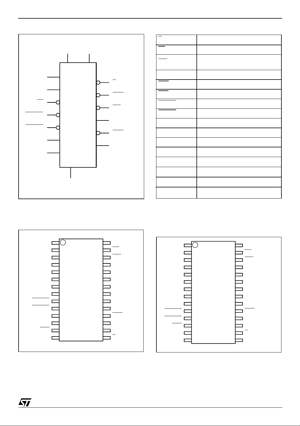
Figure 3. Logic Diagram
(1)
V
V
CC
SCL
SDA
EX
M41ST85Y
RSTIN1
M41ST85W
RSTIN2
WDI
PFI
V
Note: 1. For 28-pin , 300mil emb edded crystal SOIC only.
SS
BAT
E
CON
RST
IRQ/FT/OUT
SQW
PFO
V
OUT
AI03658
Table 1. Signal Names
E
CON
EX External Chip Enable
/FT/OUT
IRQ
PFI Power Fail Input
PFO
RST
RSTIN1
RSTIN2
SCL Serial Clock Input
SDA Serial Data Input/Output
SQW Square Wave Output
WDI Watchdog Input
V
CC
V
OUT
V
SS
(1)
V
BAT
Note: 1. For 28-pin , 300mil emb edded crystal SOIC only.
Conditioned Chip Enable Output
Interrupt/Frequency T est/Out Output
(Open Drain)
Power Fail Output
Reset Output (Open Drain)
Reset 1 Input
Reset 2 Input
Supply Voltage
Voltage Output
Ground
Battery Supply Voltage
Figure 4. 28-pin SOIC Connections Figure 5. 28-pin, 300mil SOIC (MX)
Connections
SQW V
NC
NC
NC
NC
NC
NC
WDI
RSTIN1
RSTIN2
NC
1
2
3
4
5
6
7
M41ST85Y
M41ST85W
8
9
10
11
12
PFO
V
SS
13
14
28
27
26
25
24
23
22
21
20
19
18
17
16
15
AI03659
CC
EX
IRQ/FT/OUT
V
OUT
NC
NC
PFI
NC
SCL
NC
RST
NCNC
SDA
E
CON
NC V
NC
NC
NC
NC
NC
NC
SQW
WDI
RSTIN1
RSTIN2
PFO
NC
V
SS
1
2
3
4
5
6
7
M41ST85Y
M41ST85W
8
9
10
11
12
13
14
28
27
26
25
24
23
22
21
20
19
18
17
16
15
EX
IRQ/FT/OUT
V
V
PFI
SCL
NC
NC
RST
NC
SDA
E
V
CC
OUT
SS
CON
BAT
AI06370c
5/33
Page 6
M41ST85Y, M41ST85W
Figure 6. Block Diagram
SDA
SCL
(2)
Crystal
I2C
INTERFACE
32KHz
OSCILLA T OR
REAL TIME CLOCK
CALENDAR
44 BYTES
USER RAM
RTC w/ALARM
& CALIBRATION
WATCHDOG
SQUARE W AVE
AFE
WDS
IRQ/FT/OUT
SQW
(1)
WDI
V
CC
V
BA T
VBL= 2.5V
V
SO
V
PFD
RSTIN1
RSTIN2
EX
PFI
1.25V
(Internal)
Note: 1. Open drain output
2. Integra ted into SOIC package for MX package opt ion.
= 2.5V
= 4.4V
(2.65V for ST85W)
COMPARE
COMPARE
COMPARE
COMP ARE
POR
BL
V
OUT
RST
E
CON
PFO
(1)
AI03932
6/33
Page 7
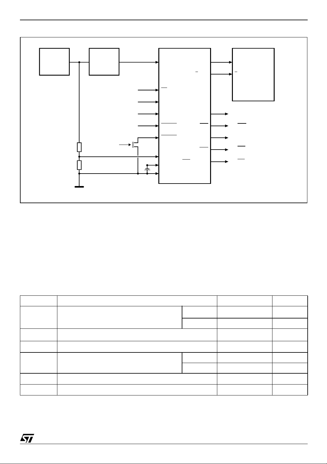
Figure 7. Hardware Hookup
M41ST85Y, M41ST85W
Unregulated
Voltage
R1
R2
Note: 1. Required for embedded crystal (MX) package only.
Regulator
V
V
IN
Pushbutton
Reset
CC
From MCU
MAXIMUM RATIN G
Stressing the device ab ove the rating listed in the
“Absolute Maximum Ratings” table may cause
permanent damage to the device. These are
stress ratings only and operation of the dev ice at
these or any other conditions above those indicated in the Operating sections of this specification is
M41ST85Y/W
V
CC
EX
SCL
WDI
RSTIN1
RSTIN2
PFI
V
BAT
V
SS
(1)
IRQ/FT/OUT
V
E
CON
SQW
OUT
SDA
RST
PFO
V
CC
E
M68Z128Y/W
or
M68Z512Y/W
To RST
To LED Display
To NMI
To INT
AI03660
not implied. Exposure to Absol ute Maxim um Ra ting conditions for extended periods may affect device reliability. Refer also to the
STMicroelectronics SURE Program and other relevant quality documents.
Table 2. Absolute Maximum Ratings
Symbol Parameter Value Unit
®
T
STG
Storage Temperature (VCC Off, Oscillator Off)
SNAPHAT
SOIC –55 to 125 °C
(1)
T
SLD
V
IO
V
CC
I
O
P
D
Note: 1. Reflow at peak temperature of 215°C to 225° C for < 60 sec onds (total thermal budg et not to exce ed 180°C for between 90 to 120
secon ds).
CAUTION: Negative und ershoots below –0.3V are not allowed on any pin while in the Bat tery Back-u p mode.
CAUTION: Do NOT wave solder SOIC to av oi d damaging SNAPHAT sockets.
Lead Solder Temperature for 10 seconds 260 °C
Input or Output Voltage
M41ST85Y –0.3 to 7 V
Supply Voltage
M41ST85W –0.3 to 4.6 V
Output Current 20 mA
Power Dissipation 1 W
–40 to 85 °C
–0.3 to V
CC
+0.3
V
7/33
Page 8
M41ST85Y, M41ST85W
DC AND AC PARAMETERS
This section summarizes the operat ing and measurement conditions, as well as the DC and AC
characteristics of the device. The parameters in
the following DC and AC Characteristic tables are
derived from tests performed under the M easure-
Table 3. DC and AC Measurement Conditions
Parameter M41ST8 5Y M41ST85W
V
Supply Voltage
CC
Ambient Operating Temperature –40 to 85°C –40 to 85°C
Load Capacitance (C
)
L
Input Rise and Fall Times ≤ 50ns ≤ 50ns
Input Pulse Voltages
Input and Output Timing Ref. Voltages
Note: Output Hi gh Z is define d as the point where data is no l onger driven.
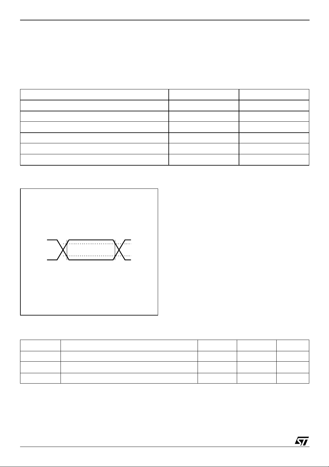
Figure 8. AC Testing Input/Output Waveforms
ment Conditions listed in the rel evant tables. Designers should check that the operating conditions
in their projects match the measurement conditions when using the quoted parameters.
4.5 to 5.5V 2.7 to 3.6V
100pF 50pF
0.2 to 0.8V
0.3 to 0.7V
CC
CC
0.2 to 0.8V
0.3 to 0.7V
CC
CC
0.8V
CC
0.2V
CC
Note: 50pF for M41ST85W.
0.7V
0.3V
AI02568
CC
CC
Table 4. Capacitance
Symbol
C
IN
(3)
C
OUT
t
LP
Note: 1. Effective capacitan ce measured wi th power supply at 5V. Sampled onl y, not 100% test ed.
2. At 25°C, f = 1MHz.
3. Outputs are deselect ed.
Input Capacitance 7 pF
Output Capacitance 10 pF
Low-pass filter input time constant (SDA and SCL) 50 ns
Parameter
(1,2)
Min Max Unit
8/33
Page 9

Table 5. DC Characteristics
Sym Parameter
Battery Current OSC
ON
(2)
I
BAT
I
I
I
Battery Current OSC
OFF
Supply Current f = 400kHz 1.4 0.75 mA
CC1
Supply Current
CC2
(Standby)
Input Leakage Current
(3)
LI
Input Leakage Current
(PFI)
Test
Condition
= 25°C,
T
A
V
= 0V,
CC
= 3V
V
BAT
SCL, SDA =
– 0.3V
V
CC
0V ≤ V
≤
IN
V
CC
M41ST85Y, M41ST85W
M41ST85Y M41ST85W
(1)
Min Typ Max Min Typ Max
400 500 400 500 nA
50 50 nA
1 0.50 mA
±1 ±1 µA
–25 2 25 –25 2 25 nA
Unit
I
LO
I
OUT1
I
OUT2
V
V
V
OHB
V
V
V
VCC – 0.3V
V
(6)
IOH = –1.0mA
I
IOL = 10mA
V
VCC = 3V(V)
0V ≤ V
BAT
OL
CC
Output Leakage
(4)
Current
(5)
V
Current (Active)
OUT
V
Current (Battery
OUT
Back-up)
V
Input High Voltage
IH
V
Input Low Voltage –0.3
IL
Battery Voltage 2.5 3.0
BAT
OH
Output High Voltage
(7)
VOH (Battery Back-up)
Output Low Voltage
OL
Output Low Voltage
(Open Drain)
Power Fail Deselect 4.20 4.40 4.50 2.55 2.60 2.70 V
PFD
(8)
PFI Input Threshold
PFI
IN
V
CC
V
OUT1
V
OUT2
– 0.3V
=
I
OUT2
–1.0µA
= 3.0mA
= 5V(Y)
>
>
≤
±1 ±1 µA
175 100 mA
100 100 µA
0.7V
CC
VCC + 0.3 0.7V
0.3V
3.5
CC
(9)
–0.3
2.5 3.0
CC
2.4 2.4 V
2.5 2.9 3.5 2.5 2.9 3.5 V
0.4 0.4 V
0.4 0.4 V
1.225 1.250 1.275 1.225 1.250 1.275 V
VCC + 0.3
0.3V
3.5
PFI Hysteresis PFI Rising 20 70 20 70 mV
V
Note: 1. Valid for A m bi ent Operat in g T em perature: TA = –40 to 85°C ; VCC = 4.5 to 5.5V or 2. 7 to 3.6V (exce pt where noted) .
Battery Back-up
SO
Switchover
2. Measured with V
3. RSTIN1
4. Outputs Dese l ected .
5. External SRAM must match RTC SUPERVISOR chip V
6. For PFO
7. Conditi oned outp ut (E
8. For IRQ
9. For rech argeable back-up, V
and RSTI N2 internally pulled-up t o VCC through 100KΩ resistor. WDI internally pulled-down to VSS through 100KΩ resistor.
and SQW pins (CMOS) .
duce batter y li fe.
/FT/OUT, RST pins (Ope n Drai n): i f pu ll ed- up to supp ly oth e r tha n VCC, this su ppl y mu st be equ al to, or l es s t han 3. 0V when
V
= 0V (durin g battery back -up mode).
CC
OUT
and E
CON
open.
CON
) can only sust ain CMOS le akage curren t in the ba tter y ba ck-u p mode . Highe r leak ag e curre nts w ill re -
(max) may be considered VCC.
BAT
specification.
CC
2.5 2.5 V
(9)
CC
V
V
V
9/33
Page 10

M41ST85Y, M41ST85W
OPERATING MODES
The M41ST85Y/W clock operates as a slave device on the serial bus. Access is obtained by implementing a start condition followed by the
correct slave address (D0h). The 64 bytes contained in the device can then be accessed sequentially in the following order:
1. Tenths/Hundredths of a Second Register
2. Seconds Register
3. Minutes Register
4. Century/Hours Register
5. Day Register
6. Date Register
7. Month Register
8. Year Register
9. Control Register
10. Watchdog Register
11 - 16. Alarm Registers
17 - 19. Reserved
20. Square Wave Register
21 - 64. User RAM
The M41ST85Y/W clock continually monitors V
for an out-of-tolerance condition. Should VCC fall
below V
, the device terminates an access in
PFD
progress and resets t he device address counter.
Inputs to the device will not be recognized at this
time to prevent erroneous dat a f rom bei ng wri tten
to the device from a an out-of-tolerance system.
When V
falls below VSO, the device a utomati-
CC
cally switches over to the battery and powers
down into an ultra low current mode of operation to
CC
conserve bat tery life. As system p ower returns an d
rises above VSO, the battery is disconnected,
V
CC
and the power supply is switched to external V
Write protection continues until V
V
(min) plus t
PFD
REC
(min).
CC
CC
reaches
For more information on Battery Storage Life refer
to Application Note AN1012.
2-Wire Bus Characteristics
The bus is intended for communication between
different ICs. It consists of two lines: a bi-directional data signal (SDA) and a clock signal (SCL).
Both the SDA and SCL lines must be connected to
a positive supply voltage via a pull-up resistor.
The following protocol has been defined:
– Data transfer may be initiated only when the bus
is not busy.
– During data transfer, the data line must remain
stable whenever the clock line is High.
– Changes in the data line, while the clock line is
High, will be interpreted as control signals.
Accordingly, the following bus conditions have
been defined:
Bus not busy. Both data and clock lines remain
High.
Start data transfer. A c hange in the st ate of the
data line, from High to Low, while the clock is High,
defines the START condition.
Stop data transfer. A change in the state of the
data line, from Low to High, while the clock is High,
defines the STOP condition.
.
10/33
Page 11

M41ST85Y, M41ST85W
Data Valid. The state of the data line represents
valid data when after a start condition, the data line
is stable for the duration of the high period of the
clock signal. The data on the line may be changed
during the Low period of the clock signal. There is
one clock pulse per bit of data.
Each data transfer is initiated with a start condition
and terminated with a stop condition. The number
of data bytes transferred between the start and
stop conditions is not limited. The information is
transmitted byte-wide and each receiver acknowledges with a ninth bit.
By definition a device that gives out a message is
called “transmitter,” the receiving device that gets
the message is called “receiver.” The device that
controls the message is called “master.” The devices that are controlled by the master are call ed
“slaves.”
Figure 9. Serial Bus Data Transfer Sequence
DATA LINE
STABLE
DATA VALID
Acknowledge. Each byte of eight bits is followed
by one Acknowledge Bit. This Acknowledge Bit is
a low level put on the bus by the receiver whereas
the master generates an extra acknowledge related clock pulse. A slave receiver which is addressed is obliged to generate an acknowledge
after the reception of each byte that has been
clocked out of the slave transmitter.
The device that acknowledges has to pull down
the SDA line during the acknowledge clock pulse
in such a way that the SDA line is a stable Low during the High period of the acknowledge related
clock pulse. Of course, setup and hold times must
be taken into account. A master receiver must signal an end of data to the slave transm itter by not
generating an acknowledge on t he last byte that
has been clocked out of the slave. In this case the
transmitter must leave the data line High to enable
the master to generate the STOP condition.
CLOCK
DATA
START
CONDITION
Figure 10. Acknowledgement Sequence
START
SCL FROM
MASTER
DATA OUTPUT
BY TRANSMITTER
DATA OUTPUT
BY RECEIVER
12 89
MSB LSB
CHANGE OF
DATA ALLOWED
STOP
CONDITION
AI00587
CLOCK PULSE FOR
ACKNOWLEDGEMENT
AI00601
11/33
Page 12

M41ST85Y, M41ST85W
Figure 11. WRITE Cycle Timing: RTC & External SRAM Control Signals
EX
tEXPD
tEXPD
E
CON
Figure 12. Bus Timing Requirements Sequence
SDA
AI03663
tHD:STA
tSU:STOtSU:STA
P
AI00589
SCL
tHD:STAtBUF
tR
SP
tHIGH
tLOW
tF
tSU:DAT
tHD:DAT
SR
Table 6. AC Characteristics
Symbol
f
SCL
t
BUF
t
EXPD
t
F
t
HD:DAT
t
HD:STA
t
HIGH
t
LOW
t
R
t
SU:DAT
t
SU:STA
t
SU:STO
Note: 1. Valid for A m bi ent Operat in g T em perature: TA = –40 to 85°C ; VCC = 4.5 to 5.5V or 2. 7 to 3.6V (exce pt where noted) .
2. Transmitter must internally provide a hold time to bridge the undefined region (300ns max) of the falling edge of SCL.
SCL Clock Frequency 0 400 kHz
Time the bus must be free before a new transmission can start 1.3 µs
EX to E
Propagation Delay
CON
SDA and SCL Fall Time 300 ns
(2)
Data Hold Time 0 µs
START Condition Hold Time
(after this period the first clock pulse is generated)
Clock High Period 600 ns
Clock Low Period 1.3 µs
SDA and SCL Rise Time 300 ns
Data Setup Time 100 ns
START Condition Setup Time
(only relevant for a repeated start condition)
STOP Condition Setup Time 600 ns
Parameter
(1)
Min Max Unit
M41ST85Y 10
M41ST85W 15
600 ns
600 ns
ns
12/33
Page 13

READ Mode
In this mode the master reads th e M41ST85Y/W
slave after setting the slave address (see Figure
13, page 13). Following the WRITE Mode Cont rol
Bit (R/W
=0) and the Acknowledge Bit, the word
address 'An' is written to the on-chip address
pointer. Next the START condition and slave address are repeated followed by the READ Mode
Control Bit (R/W
=1). At this point the master trans-
mitter becomes the master receiver.
The data byte which was add ressed will be trans-
mitted and the master receiver will send an Acknowledge Bit to the slave transmitter. The
address pointer is only i ncremented on reception
of an Acknowledge Clock. The M41ST85Y/W
slave transmitter will now place the data byte at
address An+1 on the bus, the master receiver
reads and acknowledges the new byte and the address pointer is incremented to An+2.
Figure 13. Slave Address Location
M41ST85Y, M41ST85W
This cycle of reading con secutive addresses will
continue until the mast er receiver sends a STOP
condition to the slave transmitter (see F igure 14,
page 13).
The system-to-user transfer of clock data will be
halted whenever the address being read is a clock
address (00h to 07h). The update will resum e either due to a Stop Condition or when the pointer
increments to a non-clock or RAM address.
Note: This is true both in READ Mode and WRITE
Mode.
An alternate READ Mode may also be implemented whereby the master reads the M41ST85Y/W
slave without first writing to the (volatil e) address
pointer. The first address that is read is the last
one stored in the pointer (see Figure 15, page 14).
R/W
START A
Figure 14. READ Mode Sequence
BUS ACTIVITY:
MASTER
SDA LINE
BUS ACTIVITY:
START
S
ADDRESS
R/W
ADDRESS (An)
ACK
SLAVE
DATA n+X
WORD
MSB
STOP
P
SLAVE ADDRESS
0100011
START
S
ACK
SLAVE
ADDRESS
LSB
AI00602
R/W
DATA n DATA n+1
ACK
ACK
ACK
NO ACK
AI00899
13/33
Page 14

M41ST85Y, M41ST85W
Figure 15. Al te rnat e R E A D Mo de S equence
BUS ACTIVITY:
MASTER
BUS ACTIVITY:
START
S
SLAVE
ADDRESS
R/W
DATA n DATA n+1 DATA n+X
ACK
WRITE Mode
In this mode the master transmitter transmits to
the M41ST85Y/W slave receiver. Bus protocol is
shown in Figure 16, page 14. Following the
START condition and slave address, a logic '0' (R/
=0) is placed on the bus and indicates to the ad-
W
dressed device that word address An will follow
and is to be written to the on-chip address pointer.
The data word to be written to the memory is
Figure 16. WRITE Mode S equence
BUS ACTIVITY:
MASTER
START
R/W
STOP
PSDA LINE
ACK
ACK
ACK
NO ACK
AI00895
strobed in next and the internal address pointer is
incremented to the next memory location within
the RAM on the reception of an acknowledge
clock. The M41ST85Y/W sla ve receiver will send
an acknowledge clock to the master transmitter after it has received the slave address (see Figure
13, page 13) and aga in after it has received the
word address and each data byte.
STOP
BUS ACTIVITY:
S
ADDRESS
SLAVE
WORD
ADDRESS (An)
ACK
DATA n DATA n+1 DATA n+X
ACK
ACK
ACK
PSDA LINE
ACK
AI00591
14/33
Page 15

Data Retention Mode
With valid V
applied, the M 41ST85Y /W can be
CC
accessed as described above with READ or
WRITE Cycles. Should the s upply voltage d ecay,
the M41ST85Y/W will automatically deselect,
write protecting itself (and any external SRAM)
when V
V
(min). Th is is accomplish ed by internally in-
PFD
falls between V
CC
(max) and
PFD
hibiting access to the clock registers. At this time,
the R eset pin (RS T
main active until V
) is driven active and will re-
returns to nominal levels. Ex-
CC
ternal RAM access is inhibited in a similar manner
by forcing E
0.2 volts of the V
as long as V
dition. When V
Switchover Voltage (V
from the V
to a high level. This level is within
CON
CC
CC
BAT
. E
will remain at this level
CON
remains at an out-of-tolerance con-
falls below the Battery Back-up
CC
), power input is switched
SO
pin to the SNAPHAT® battery, and
the clock registers and external SRAM are m aintained from the attached battery supply.
All outputs become high impedance. The V
OUT
pin
is capable of supplying 100 µA of current to the attached memory with less than 0.3 volts drop under
this condition. On power up, when V
returns to
CC
a nominal value, write protection continues for
by inhibiting E
t
REC
. The RST signal also re-
CON
mains active during this time (see Figure 17, page
16).
Note: Most low power SRAMs on the market to-
day can be used with the M41ST85Y /W RTC S UPERVISOR. There are, however some criteria
which should be used in making the final choice of
M41ST85Y, M41ST85W
an SRAM to use. The SRAM must be designed in
a way where the chip enable input disables all other inputs to the SRAM. This allows inputs to t he
M41ST85Y/W and SRAMs to be “Don’t Care”
once V
should also guarantee data retention down to
V
CC
be sufficient to meet the system needs with the
chip enable output propagation delays included. If
the SRAM includes a second chip enable pin (E2),
this pin should be tied to V
If data retention lifetime is a critical parameter f or
the system, it is importa nt to re view the dat a retention current specifications for the particular
SRAMs being evaluated. M ost SRAMs specify a
data retention current at 3.0 volts. Manufacturers
generally specify a typical condition for room temperature along with a worst case condition (generally at elevated temperatures). The system level
requirements will determine the choice of which
value to use. Th e data retention current value of
the SRAMs can then be added to the I
the M41ST85Y/W to determine the total current requirements for data retention. The available battery capacity for the SNAPHAT
can then be divided b y this current to determine
the amount of data retention ava ilable (see Table
15, page 27).
For a further more detailed review of lifetime calculations, please see Application Note AN1012.
falls below V
CC
(min). The SRAM
PFD
=2.0 volts. The chip enable access time must
.
OUT
value of
BAT
®
of your choice
15/33
Page 16

M41ST85Y, M41ST85W
Figure 17. Power Down/Up Mode AC Waveforms
V
CC
V
(max)
PFD
V
(min)
PFD
VSO
INPUTS
RST
OUTPUTS
E
CON
tPD
PFO
(PER CONTROL INPUT)
tF
VALID VALID
tFB
tDR
tRB
DON'T CARE
HIGH-Z
tR
tREC
RECOGNIZEDRECOGNIZED
(PER CONTROL INPUT)
AI03661
Table 7. Power Down/Up AC Characteristics
Symbol
(2)
t
F
t
FB
t
PD
t
PFD
t
R
t
RB
t
REC
Note: 1. Valid for A m bi ent Operat in g T em perature: TA = –40 to 85°C ; VCC = 4.5 to 5.5V or 2. 7 to 3.6V (exce pt where noted) .
2. V
3. V
4. Programmable (see Table 12, page 25)
V
(max) to V
PFD
(3)
V
(min) to VSS VCC Fall Time
PFD
EX at VIH before Power Down
PFI to PFO Propagation Delay 15 25 µs
V
(min) to V
PFD
VSS to V
(4)
Power up Deselect Time 40 200 ms
(max) to V
PFD
200µs after V
PFD
CC
(min) to VSS fall time of less than tFB may cause corruption of RAM data.
(min) VCC Rise Time
PFD
(min) fall time of less than tF may result in deselection/write protection not occurring until
PFD
passes V
Parameter
(min) VCC Fall Time
PFD
(max) VCC Rise Time
PFD
(min).
PFD
(1)
Min Typ Max Unit
300 µs
10 µs
0µs
10 µs
1µs
16/33
Page 17

CLOCK OPERATION
The eight byte clock register (see Table 8, page
18) is used to both set the clock and t o read the
date and time from the clock, in a binary coded
decimal format. Tenths/Hundredths of Seconds,
Seconds, Minutes, and Hours are contained within
the first four registers.
Note: A WRIT E to any c lock reg ister w ill resu lt in
the Tenths/Hundredths of Seconds bei ng reset to
“00,” and Tenths/Hundredths of Seconds cannot
be written to any value other than “00.”
Bits D6 and D7 of Clock Register 03h (Century/
Hours Register) contain the CENTURY ENABLE
Bit (CEB) and the CENTURY Bit (CB). Setting
CEB to a '1' will cause CB to toggle, either from '0'
to '1' or from '1' to '0' at the turn of the century (depending upon its initial state). If CEB is set to a '0,'
CB will not toggle. Bits D0 through D2 of Regi ster
04h contain the Day (day of week). Registers 05h,
06h, and 07h contain the Date (day of month),
Month and Years. The ninth clock register is the
Control Register (this is described in the Clock
Calibration section). Bit D7 of Register 01h contains the S TOP Bit (ST). Setting this bit to a ' 1 ' wil l
cause the oscillator to stop. If the device is expected to spend a significant amount of time on the
shelf, the oscillator may be stopped to reduce current drain. When reset to a '0' the oscillator restarts
within one second.
The eight Clock Registers may be read one byte at
a time, or in a sequential block. T he Control Register (Address location 08h) may be accessed independently. Provision has been made to assure
that a clock update does not occur while any of the
M41ST85Y, M41ST85W
eight clock addresses are being read. If a clock address is being read, an update of the clock registers will be halte d. This will pr event a trans ition of
data during the READ.
Note: When a power failure occurs, the Halt Update Bit (HT) will automatically be set to a '1.' This
will prevent the clock from updating the TIMEKEEPER
the exact time of the power-down event. Resetting
the HT Bit to a '0' will allow the clock to update the
TIMEKEEPER registers with the current time.
TIMEKEEPER
The M41ST85Y/W offers 20 internal registers
which contain Clock, Alarm, Watchdog, Flag,
Square Wave and Control data. These registers
are memory locations which contain external (user
accessible) and internal copies of the data (usually
referred to as BiPORT
external copies are in dependent of internal f unctions except that they are updated p eriodically by
the simultaneous transfer of the incremented internal copy. The internal divider (or clock) chain will
be reset upon the completion of a WRITE to any
clock address.
The system-to-user transfer of clock data will be
halted whenever the address being read is a clock
address (00h to 07h). The update will resum e either due to a Stop Condition or when the pointer
increments to a non-clock or RAM address.
TIMEKEEPER and Alarm Registers store data in
BCD. Control, Watchdog and Square Wave Registers store data in Binary Format.
®
registers, and will allow the user to read
®
Registers
™
TIMEKEEPER cel ls). The
17/33
Page 18

M41ST85Y, M41ST85W
Table 8. TIMEKEEPER® Register Map
Address
Data
D7 D6 D5 D4 D3 D2 D1 D0
00h 0.1 Seconds 0.01 Seconds Seconds 00-99
01h ST 10 Seconds Seconds Seconds 00-59
02h 0 10 Minutes Minutes Minutes 00-59
03h CEB CB 10 Hours Hours (24 Hour Format) Century/Hours 0-1/00-23
04h TR 0 0 0 0 Day of Week Day 01-7
05h 0 0 10 Date Date: Day of Month Date 01-31
06h 0 0 0 10M Month Month 01-12
07h 10 Years Year Year 00-99
08h OUT FT S Calibration Control
09h WDS BMB4 BMB3 BMB2 BMB1 BMB0 RB1 RB0 Watchdog
0Ah AFE SQWE ABE Al 10M Alarm Month Al Month 01-12
0Bh RPT4 RPT5 AI 10 Date Alarm Date Al Date 01-31
0Ch RPT3 HT AI 10 Hour Alarm Hour Al Hour 00-23
0Dh RPT2 Alarm 10 Minutes Alarm Minutes Al Min 00-59
Function/Ra nge
BCD Format
0Eh RPT1 Alarm 10 Seconds Alarm Seconds Al Sec 00-59
0Fh WDF AF 0 BL 0 0 0 0 Flags
10h 0 0 0 0 0 0 0 0 Reserved
11h 0 0 0 0 0 0 0 0 Reserved
12h 0 0 0 0 0 0 0 0 Reserved
13h RS3 RS2 RS1 RS0 0 0 0 0 SQW
Keys: S = Sign Bit
FT = Frequency Test Bit
ST = Stop Bit
0 = Must be set to zero
BL = Battery Low Flag (Rea d only)
BMB0-BMB4 = Watchdog Multiplier Bits
CEB = Century Enable Bit
CB = Centur y B i t
OUT = Output level
AFE = Alarm Flag Enable Flag
RB0-RB 1 = Watchdog Resolution Bit s
WDS = Watchdog Steering Bit
ABE = Alarm in Battery Back-Up Mode Enable Bit
RPT1-RPT5 = Alarm Repeat Mode Bit s
WDF = Watchdog flag (Read only)
AF = Alarm f l ag (Read only)
SQWE = Square Wave Enable
RS0-RS 3 = S Q W Frequency
HT = Halt Up date Bit
REC
Bit
TR = t
18/33
Page 19

Calib ratin g t h e C lock
The M41ST85Y/W is driven by a quartz controlled
oscillator with a nominal frequency of 32,768 Hz.
The devices are tested not exceed +/–35 PPM
(parts per million) oscillator frequency error at
o
C, which equates to about +/–1.53 minutes per
25
month. When the Calibration circuit is properly employed, accuracy improves to better than +1/–2
ppm at 25°C.
The oscillation rate of crystals changes with temperature (see Figure 21, page 26). Therefore, the
M41ST85Y/W design employs periodic counter
correction. The calibration circuit adds or subtracts
counts from the oscillator divider circuit at the divide by 256 stage, as shown in Figure 22, page 26.
The number of times pulses which are blanked
(subtracted, negative calibration) or split (added,
positive calibration) depends upon the value loaded into the five Calibration Bits found in the Control
Register. Adding counts speeds the clock up, subtracting counts slows the clock down.
The Calibration Bits occupy the five lower order
bits (D4-D0) in the Control Register (08h). These
bits can be set to represent any value between 0
and 31 in binary form. Bit D5 is a Sign Bit; '1' indicates positive calibration, '0' indicates negative
calibration. Calibration occurs within a 64 m inute
cycle. The first 62 m inutes i n t he c ycle m ay , onc e
per minute, have one second either shortened by
128 or lengthened by 256 oscillator cycles. If a binary '1' is loaded into the register, only the first 2
minutes in the 64 minute cycle will be modified; if
a binary 6 is loaded, t he first 12 will be affected,
and so on.
Therefore, each cal ibration step has the effect of
adding 512 or subtracting 256 oscillator cycles for
every 125,829,120 actual oscillator cycles, that is
+4.068 or –2.034 PPM of adjustm ent per calibration step in the cal ibration registe r. Ass um ing that
the oscillator is running at exactly 32,768 Hz, each
of the 31 increments in the Calibration byte would
represent +10.7 or –5.35 seconds per month
which corresponds to a total range of +5.5 or –2.75
minutes per month.
Two methods are available for ascertaining how
much calibration a given M41ST85Y/W may require.
The first involves setting the clock, letting it run for
a month and comparing it to a known accurate reference and recording deviation over a fixed period
of time. Calibration values, including the number of
seconds lost or gained in a given period, can be
found in Application Note AN934, “TIMEKEEP-
®
CALIBRATION.” This allows the designer to
ER
give the end user the ability to calibrate the clock
as the environment requires, even if the final prod-
M41ST85Y, M41ST85W
uct is packaged in a non-user serviceable enc losure. The designer could provide a simple utility
that accesses the Calibration byte.
The second approach is better suit ed to a manufacturing environment, and involves the use of the
IRQ
/FT/OUT pin. The pin will toggle at 512Hz,
when the Stop Bit (S T, D7 of 01h) is '0, ' the Frequency Test Bit (F T, D6 of 08h) is '1 ,' the Alarm
Flag Enable Bit (AFE, D7 of 0Ah) is '0, ' and the
Watchdog Steering Bit (WDS, D7 of 09h) is '1' or
the Watchdog Register (09h = 0) is reset.
Any deviation from 512 Hz i ndicates the degree
and direction of oscillator frequency shift at the test
temperature. For example, a reading of
512.010124 Hz would indicate a +20 PPM oscillator frequency error, requiring a –10 (XX001010) to
be loaded into the Calibration Byte for correction.
Note that setting or changing the Calibration Byte
does not affect the Frequency test output frequency.
The IRQ
which requires a pull-up resistor to V
operation. A 500 to10k resistor is recommended in
order to control the rise time. The FT Bit i s cleared
on power-down.
Setting Alarm Clock Registers
Address locations 0Ah-0Eh contain the alarm settings. The alarm can be configured to go off at a
prescribed time on a specific mont h, date, hour,
minute, or second, or repeat every year, month,
day, hour, minute, or second. It can al so be programmed to go off while the M41ST85Y/W is in the
battery back-up to serve as a system wake-up call.
Bits RPT5–RPT1 put the alarm in the repeat mode
of operation. Table 9, page 20 shows the possible
configurations. Codes not listed in the table default
to the once per second mode to quickly alert the
user of an incorrect alarm setting.
When the clock information matches the alarm
clock settings based on the m atch criteria d efined
by RPT5–RPT1, the AF (Alarm Flag) is set. If AFE
(Alarm Flag Enable) is also set, the alarm condition activates the IRQ
Figure 18, page 20. To disable alarm, write '0' t o
the Alarm Date Register and to RPT5–RPT1.
Note: If the address pointer is allowed to increment to the Flag Register address, an alarm condition will not cause the Interrupt/Flag to occur until
the address pointer is moved to a different address. It should also be noted that if the last address written is the “Alarm Seconds,” the address
pointer will increment to the Flag address, causing
this situation to occur.
/FT/OUT pin is an open drain output
for proper
CC
/FT/OUT pin as shown in
19/33
Page 20

M41ST85Y, M41ST85W
The IRQ/FT/OUT output is cleared by a READ to
the Flags Register. A subsequent READ of the
Flags Register is necessary to see that the value
of the Alarm Flag has been reset to '0.'
The IRQ
battery back-up mode. The IRQ
/FT/OUT pin can also be activated in the
/FT/OUT will go
low if an alarm occurs and both ABE (Alarm in Bat -
ABE and AFE Bits are reset during power-up,
therefore an alarm generated during power-up will
only set AF. The user can read the Flag Register
at system boot-up to determine if an alarm was
generated while the M41ST85Y/W wa s in the deselect mode during power-up. Figure 19, page 21
illustrates the back-up mode alarm timing.
tery Back-up Mode Enable) and A FE are set . The
Figure 18. Alarm Interrupt Reset Waveform
0Fh0Eh 10h
ACTIVE FLAG
IRQ/FT/OUT
HIGH-Z
Table 9. Alarm Repeat Modes
RPT5 RPT4 RPT3 RPT2 RPT1 Alarm Setting
11111Once per Second
11110Once per Minute
AI03664
11100Once per Hour
11000Once per Day
10000Once per Month
00000Once per Year
20/33
Page 21

Figure 19. Back-Up Mode Alarm Waveform
V
CC
V
PFD
V
SO
ABE, AFE Bits in Interrupt Register
AF bit in Flags Register
IRQ/FT/OUT
M41ST85Y, M41ST85W
tREC
HIGH-Z
Watchdog Timer
The watchdog timer can be used to detect an outof-control microprocessor. The user programs the
watchdog timer by setting the desired amount of
time-out into the Watchdog Register, address 09h.
Bits BMB4-BMB0 store a binary multiplier and the
two lower order bits RB1-RB0 select the resolution, where 00=1/16 second, 01=1/4 second, 10=1
second, and 11=4 seconds. The amount of timeout is then determ ined to be the multiplic ation of
the five-bit multiplier value with the resolution. (For
example: writing 00001110 in the Wa tchdo g Register = 3*1 or 3 seconds).
Note: The accuracy of the timer is within ± the selected resolution.
If the processor does not reset the timer within the
specified period, the M41ST85Y/W s ets the WD F
(Watchdog Flag) and generates a watchdog interrupt or a microprocessor reset.
The most significant bit of the Watchdog Register
is the Watchdog Steering Bit (WDS). When set to
a '0,' the wa tchdog will activ ate the IRQ
/FT/OUT
pin when timed-out. When WDS is set to a '1,' the
watchdog will output a negative pulse on the RS T
pin for t
. The Watchdog register, FT, AFE, ABE
REC
and SQWE Bits will reset t o a '0' at the end of a
Watchdog time-out when the WDS Bit is set to a
'1.'
HIGH-Z
AI03920
The watchdog timer can be reset by two methods:
1) a transition (high-to-low or low-to-high) c an be
applied to the Watchdog Input pin (WDI) or 2) the
microprocessor can perform a WRITE of the
Watchdog Register. The time-out period then
starts over.
Note: The WDI pin should be tied to V
SS
if not
used.
In order to perform a software reset of the watch-
dog timer, the original time-out period can be written into the Watchdog Register, effectively
restarting the cou nt-d o wn cycle.
Should the watchdog timer time-out, and the WDS
Bit is programmed to output an interrupt, a value of
00h needs to be written to the Watchdog Register
in order to clear the IRQ
/FT/OUT pin. This will also
disable the watchdog funct ion until i t is agai n programmed correctly. A READ of the Flags Register
will reset the Watchdog Flag (Bit D7; Register
0Fh).
The watchdog function is automatically disabled
upon power-up and the Watchdog Register is
cleared. If the watchdog function is set to output to
the I RQ
/FT/OUT pin and the frequency test function is activated, the watchdog function prevails
and the frequency test function is denied.
21/33
Page 22

M41ST85Y, M41ST85W
Square Wave Output
The M41ST85Y/W of fers the user a programmable square wave function which is output on the
SQW pin. RS3-RS0 bi ts located in 13h establish
the square wave output frequency. These frequencies are listed in Table 10. Once the selection
Table 10. Square Wave Output Frequency
Square Wave Bits Square Wave
RS3 RS2 RS1 RS0 Frequency Units
0 0 0 0 None –
0 0 0 1 32.768 kHz
0 0 1 0 8.192 kHz
0 0 1 1 4.096 kHz
0 1 0 0 2.048 kHz
0 1 0 1 1.024 kHz
0 1 1 0 512 Hz
0 1 1 1 256 Hz
1 0 0 0 128 Hz
100164Hz
101032Hz
101116Hz
11008Hz
11014Hz
11102Hz
11111Hz
of the SQW frequency has been c ompleted, the
SQW pin can be turned on and off under software
control with the Square Wave Enable Bit (S QWE)
located in Register 0Ah.
22/33
Page 23

M41ST85Y, M41ST85W
Power-on Reset
The M41ST85Y/W continuously monitors V
When V
the RST
power-up for t
The RST
falls to the power fail detect trip point,
CC
pulls low (open drain) and remains low on
after VCC passes V
REC
pin is an open drain output and an appro-
PFD
CC
(max).
priate pull-up resistor should be chosen to cont rol
rise time.
Figure 20. RSTIN1
RSTIN1
RSTIN2
RST
Note: With pull-up resi s tor
& RSTIN2 Timing Wa vef orm s
tRLRH1
(1)
tR1HRH tR2HRH
Reset Inputs (RSTIN1
.
The M41ST85Y/W provides two independ ent in-
& RSTIN2)
puts which can generate an output reset. The duration and function of these resets is identical to a
reset generated by a power cycle. Ta ble 11 and
Figure 20 illustrate the AC reset characteristics of
this function. Pulses shorter than t
t
will not generate a reset condition. RSTIN1
RLRH2
and RSTIN2 are each internally pull ed up to V
through a 100kΩ resistor.
tRLRH2
AI03665
RLRH1
and
CC
Table 11. Reset AC Characteristics
Symbol
(2)
t
RLRH1
(3)
t
RLRH2
(4)
t
R1HRH
(4)
t
R2HRH
Note: 1. Valid for A m bi ent Operat in g T em perature: TA = –40 to 85°C ; VCC = 4.5 to 5.5V or 2. 7 to 3.6V (exce pt where noted) .
2. Pulse width less than 50ns will result in no RESET (for noise immunity).
3. Pulse width less than 20ms will result in no RESET (for noise immunity).
4. Programmable (see Table 12, page 25).
RSTIN1 Low to RSTIN1 High 200 ns
RSTIN2 Low to RSTIN2 High 100 ms
RSTIN1 High to RST High 40 200 ms
RSTIN2 High to RST High 40 200 ms
Parameter
(1)
Min Max Unit
23/33
Page 24

M41ST85Y, M41ST85W
Power-fail INPUT/OUTPUT
The Power-Fail Input (PFI) is compared to an internal reference voltage (1.25V). If PFI is less than
the power-fail threshold (V
Output (PFO)
will go low. This function is intended
for use as an undervoltage detector to signal a failing power supply. Typically PFI is connected
through an external voltage divider (see Figure 7,
page 7) to either the unregula ted DC input (if it is
available) or the regulated output of the V
lator. The voltage divider can be set up such that
the voltage at PFI falls below V
onds before the regulated V
M41ST85Y/W or t he m icroproc essor drops below
the minimum operating voltage.
During battery back-up, the power-fail comparator
turns off and PFO
curs after V
er returns, PFO
goes (or remains) low. This oc-
drops below V
CC
is forced high, irrespective of V
for the write protect time (t
from V
(max) until the inputs are recognized. At
PFD
the end of this time, the power-fail comparator is
enabled and PFO
follows PFI. If the comparator is
unused, PFI should be connected to V
left unconnected.
Century Bit
Bits D7 and D6 of Clock Register 03h contain the
CENTURY ENABLE Bit (CEB) and the CENTURY
Bit (CB). Setting CEB to a '1' will cause CB to toggle, either from a '0' to '1' or from '1' to '0' at the turn
of the century (depending upon its initial state). If
CEB is set to a '0,' CB will not toggle.
Output Driver Pin
When the FT Bit, AFE B it and watchdog register
are not set, the IRQ
/FT/OUT pin becomes an output driver that reflects the contents of D7 of the
Control Register. In other words, when D7 (OUT
Bit) and D6 (FT Bit) of address location 08h are a
'0,' then the IRQ
Note: The IRQ
/FT/OUT p in w ill be dr iv en lo w .
/FT/OUT pin is an open drain which
requires an external pull-up resistor.
Battery Low Warning
The M41ST85Y/W auto matically perf orms bat tery
voltage monitoring upon power-up and at factoryprogrammed time intervals of approximately 24
hours. The Battery Low (BL) Bit, Bit D4 of Flags
Register 0Fh, will be asserted if the battery voltage
is found to b e less than approximately 2.5V. T he
), the Power-Fail
PFI
several millisec-
PFI
input to the
CC
(min). When pow-
PFD
), which is the time
REC
SS
regu-
CC
PFI
and PFO
BL Bit will remain asserted until completion of battery replacement and subsequent battery low
monitoring tests, either during the nex t power-up
sequence or the next scheduled 24-hour interval.
If a battery low is generated during a power-up sequence, this indicates that the battery is below approximately 2.5 volts and may not be able to
maintain data integrity in the SRAM. Data sho uld
be considered suspect an d verified as correct. A
fresh battery should be installed.
If a battery low indication is generated during the
24-hour interval check, this indicates that the battery is near end of life. However, data is not compromised due to the fact that a nominal V
CC
is
supplied. In order to insure data integrity during
subsequent periods of bat tery back-up m ode, the
battery should be replaced. The SNAPHAT top
may be replaced while V
is applied to the de-
CC
vice .
Note: This will cause the clock to lose time during
the interval the SNAPHAT battery/crystal top is
disconnected.
The M41ST85Y/W only monitors the battery when
a nominal V
is applied to the device. Thus appli-
CC
cations which require extensive durations in the
battery back-up mode should be powered-up periodically (at least once every few months) in order
for this technique to be beneficial. Additionally, if a
battery low is indicated, data integrity should be
verified upon power-up via a checksum or other
technique.
Bit
t
REC
Bit D7 of Clock Register 04h contains the t
(TR). t
the des elect time af ter V
refers to the automatic continuation of
REC
reaches V
CC
PFD
Bit
REC
. This al lows for a voltage settling time before WRITEs
may again be performed to the device after a power-down condition. The t
Bit will allow the u s er
REC
to set the length of this deselect time as defined by
Table 12, page 25.
Initial Power-on Defaults
Upon initial application of power to the device, the
following register bits are set to a '0' state: Watchdog Register, FT, AFE, ABE, SQWE, and TR. The
following bits are set to a '1' state: ST, OU T, and
HT (see Table 13, page 25).
24/33
Page 25

M41ST85Y, M41ST85W
Table 12. t
t
REC
REC
Bit (TR)
Definitions
STOP Bit (ST)
0 0 96 98 ms
0140
1 X 50 2000 µs
Note: 1. Default Set ting
Table 13. Default Values
Condition TR ST HT Out FT AFE ABE SQWE
Initial Power-up
Subsequent Power-up (with
battery back-up)
Note: 1. WDS, BMB0-BMB4, RB 0, RB1.
2. State of other contro l b its undefined .
3. UC = Unchanged
(2)
(3)
t
Time
REC
Units
Min Max
200
(1)
ms
WATCHDOG
Register
(1)
0111000 0 0
UC UC 1 UC 0 0 0 0 0
25/33
Page 26

M41ST85Y, M41ST85W
Figure 21. Crystal Accuracy Across Temp eratur e
Frequency (ppm)
20
0
–20
–40
–60
–80
–100
–120
–140
–160
0 10203040506070
∆F
F
Temperature °C
= -0.038 (T - T
ppm
2
C
T0 = 25 °C
)2 ± 10%
0
80–10–20–30–40
AI00999
Figure 22. Cal ib rat i on Waveform
NORMAL
POSITIVE
CALIBRATION
NEGATIVE
CALIBRATION
AI00594B
26/33
Page 27

M41ST85Y, M41ST85W
PART NUMBERING
Table 14. Ordering Information Scheme
Example: M41ST 85Y MH 6 TR
Device Type
M41ST
Supply Voltage and Write Protect Voltage
85Y = V
85W = V
Package
MH
MX
= 4.5 to 5.5V; 4.20V ≤ V
CC
= 2.7 to 3.6V; 2.55V ≤ V
CC
(1)
= SOH28
(2)
= SOX28
PFD
PFD
≤ 4.50V
≤ 2.70V
Temperature Rang e
6 = –40 to 85°C
Shipping Method for SOIC
blank = Tubes
TR = Tape & Reel
Note: 1. The 28-pi n S O IC package (S OH28) requires the battery/crystal pac kage (SNAP HA T®) which is ordered s eparately under the p art
number “M 4T XX-BR12SHX” in plastic tube or “M4TXX-BR12SHXTR” in T ape & Reel form.
2. The SOX28 package incl udes an embedded 32,768Hz crystal .
Caution: Do not place the S NAPHAT bat tery pac kage “M4TXX-BR12SH” in conductive foam as i t will drai n t he l ithi um but ton-ce ll bat tery.
For a list of available options (e.g., Speed, Package) or for further information on any aspect of this device,
please contact the ST Sales Office nearest to you.
Table 15. SNAPHAT Battery Table
Part Number Description Package
M4T28-BR12SH Lithium Battery (48mAh) and Crystal SNAPHAT SH
M4T32-BR12SH Lithium Battery (120mAh) and Crystal SNAPHAT SH
27/33
Page 28

M41ST85Y, M41ST85W
PACKAGE MECHANICAL INFORMATION
Figure 23. SOH28 – 28-lead Plastic Small Outline, Battery SNAPHAT, Package Outline
A2
A
C
Be
eB
CP
D
N
E
H
LA1 α
1
SOH-A
Note: Drawing is not to scale.
Table 16. SOH28 – 28-lead Plastic Small Outline, battery SNAPHAT, Package Mechanical Data
Symbol
A 3.05 0.120
A1 0.05 0.36 0.002 0.014
A2 2.34 2.69 0.092 0.106
B 0.36 0.51 0.014 0.020
C 0.15 0.32 0. 006 0.012
D 17.71 18.49 0.697 0.728
E 8.23 8.89 0.324 0.350
e 1.27 – – 0.050 – –
eB 3.20 3.61 0.126 0.142
H 11.51 12.70 0.453 0.500
L 0.41 1.27 0.016 0.050
α 0° 8° 0° 8°
N 28 28
CP 0.10 0.004
Typ Min Max Typ Min Max
millimeters inches
28/33
Page 29

M41ST85Y, M41ST85W
Figure 24. SH – 4-pin SNAPHAT Housing for 48mAh Battery & Crystal, Package Outline
A2
A3
L
eA
D
A1
A
B
eB
E
SHTK-A
Note: Drawing is not to scale.
Table 17. SH – 4-pin SN AP HAT Hous i n g for 48mA h Batt ery & Crystal, Package Mechanical Data
Symbol
A 9.78 0.3850
A1 6.73 7.24 0.2650 0.2850
A2 6.48 6.99 0.2551 0.2752
A3 0.38 0.0150
B 0.46 0.56 0.0181 0.0220
D 21.21 21.84 0.8350 0.8598
E 14.22 14.99 0.5598 0.5902
eA 15.55 15.95 0.6122 0.6280
eB 3.20 3.61 0.1260 0.1421
L 2.03 2.29 0.0799 0.0902
T yp Min Max Typ Min Max
millimeters inches
29/33
Page 30

M41ST85Y, M41ST85W
Figure 25. SH – 4-pi n SNAPHAT Housin g for 120mAh Batt ery & Crystal, Package Outline
A2
A3
L
eA
D
A1
A
B
eB
E
SHTK-A
Note: Drawing is not to scale.
Table 18. SH – 4-pin SNAPH AT Housing for 120mAh Battery & Crystal, Package Mechanical Data
Symbol
A 10.54 0.4150
A1 6.73 7.24 0.2650 0.2850
A2 6.48 6.99 0.2551 0.2752
A3 0.38 0.0150
B 0.46 0.56 0.0181 0.0220
D 21.21 21.84 0.8350 0.8598
E 14.22 14.99 0.5598 0.5902
eA 15.55 15.95 0.6122 0.6280
eB 3.20 3.61 0.1260 0.1421
L 2.03 2.29 0.0799 0.0902
T yp Min Max Typ Min Max
millimeters inches
30/33
Page 31

M41ST85Y, M41ST85W
Figure 26. SOX28 – 28-lead Plastic Small Outline, 300mils, Embedded Crystal, Package Outline
D
14
1
h x 45û
C
E
H
15
28
AA2
B
e
A1
ddd
LA1 α
SO-E
Note: Drawing is not to scale.
Table 19. SOX28 – 28-lead Plastic Small Outline, 300mils, Embedded Crystal, Package Mechanical
Symbol
A 2.44 2.69 0.096 0.106
A1 0.15 0.31 0.006 0.012
A2 2.29 2.39 0.090 0.094
B 0.41 0.51 0.016 0.020
C 0.20 0.31 0.008 0.012
D 17.91 18.01 0.705 0.709
ddd 0.10 0.004
E 7.57 7.67 0.298 0.302
e 1.27 – – 0.050 – –
H 10.16 10.52 0.400 0.414
L 0.51 0.81 0.020 0.032
α 0° 8° 0° 8°
N 28 28
T yp Min Max Typ Min Max
millimeters inches
31/33
Page 32

M41ST85Y, M41ST85W
REVISION HIST ORY
Table 20. Document Revision History
Date Rev. # Revision Details
August 2000 1.0 First issue
24-Aug-00 1.1 Block Diagram added (Figure 3)
t
12-Oct-00 1.2
18-Dec-00 2.0 Reformatted, TOC added, and PFI Input Leakage Current added (Table 5)
18-Jun-01 2.1
22-Jun-01 2.2 Note added to Clock Operation section
26-Jul-01 3.0 Change in Product Maturity
07-Aug-01 3.1 Improve text in “Setting the Alarm Clock” section
20-Aug-01 3.2
06-Sep-01 3.3
Table removed, cross references corrected
REC
Addition of t
information, table changed, one added (Tables 8, 12); changed PFI/PFO
REC
graphic (see Figure 6); change to DC and AC Characteristics, Order Information (T ables 5,
6, 14); note added to “Setting Alarm Clock Registers” section; added temp./voltage info. to
tables (Table 4, 5, 6, 6, 7); addition of Default Values (Table 13)
Change V
DC Characteristics V
values in document
PFD
BAT
changed; V
changed; PFI Hysteresis (PFI Rising) spec.
OHB
added; and Crystal Electrical Characteristics table removed (Tables 5, 6)
03-Dec-01 3.4
01-May-02 3.5
Changed READ/WRITE Mode Sequences (Figure 14, 16); change in V
5V (M41ST85Y) part only (Table 5, 14)
Change t
Definition (Table 12); modify reflow time and temperature footnote (Table 2)
REC
lower limit for
PFD
03-Jul-02 3.6 Modify DC Characteristics table footnote, Default Values (Tables 5, 13)
15-Nov-02 3.7
Added embedded crystal (MX) package option; corrected initial power-up condition (Figure
2, 3, 5, 6, 7, 26, Table 1, 13, 14, 19)
24-Jan-03 3.8 Update diagrams (Figure 6, 7, 26); update values (Table 7, 11, 12, 13, 19)
25-Feb-03 4.0 New Si changes (Table 7, 11, 12); corrected dimensions (Figure 26; Table 19)
32/33
Page 33

M41ST85Y, M41ST85W
M41ST85, M41ST85Y, M41ST85W, 41ST85, ST85, SUPERVISOR, SUPERVISOR, SUPERVISOR, SUPERVISOR, SUPERVISOR, SUPERVISOR, SUPERVISOR, SUPERVISOR, SUPERVISOR, SUPERVISOR, SUPERVISOR, SUPERVISOR, SUPERVISOR, SUPERVISOR, SUPERVISOR, SUPERVISOR, SUPERVISOR, SUPERVISOR, SUPERVISOR, Serial, Serial, Serial, Serial, Serial, Serial, Serial, Serial,
Serial, Serial, Serial, Serial, Serial, Serial, Serial, Serial, Serial, Serial, Serial, Serial, Serial, Serial, Serial, Serial, Serial, Serial, Serial, Serial, Serial, Serial, Serial, Serial, Serial, Serial, Serial, Serial, Serial, Serial,
Serial, Serial, Serial, Serial, Serial, Serial, Serial, Serial, Serial, Serial, Serial, Serial, Serial, Serial, Serial, Serial, Serial, RTC, RTC, RTC, RTC, RTC, RTC, RTC, RTC, RTC, RTC, RTC, RTC, RTC, RTC, RTC,
RTC, RTC, RTC, RTC, RTC, RTC, RTC, RTC, RTC, RTC, RTC, RTC, RTC, RTC, RTC, RTC, RTC, RTC, RTC, RTC, RTC, RTC, RTC, RTC, RTC, RTC, RT C, RTC, RTC, RTC, RT C, RTC, RTC, RTC, RTC,
RTC, RTC, RTC, RTC, RTC, RTC, RTC, RTC, RTC, RTC, RTC, RTC, RTC, RTC, RTC, RTC, RTC, RTC, RTC, RTC, Microprocessor, Microprocessor, Microprocessor, Microprocessor, Microprocessor, Microprocessor, Microprocessor, Microprocessor, Microprocessor, Microprocessor, Microprocessor, Microprocessor, Microprocessor, Microprocessor, Microprocessor, Microprocessor, Microproce ssor, Microprocessor, Micr oprocess or , Microprocessor, M icroproce ssor, Mic r oprocesso r , M i cr oprocess or , Microprocessor, Microprocessor, I2 C , I 2C , I2C, I2C, I2C, I2C, I2C, I2C, I2C, I2C, I2C, I2C, I2C, I2C, I2C, I2C, I2C, I2C,
I2C, I2C, I2C, I2C, I2C, I2C, I2C, I2C, I2C, I2C, I2C, I2C, I2C, I2C, I2C, I2C, I2C, I2C, I2C, I2C, I2C, I2C, I2C, I2C, I2C, I2C, I2C, I2C, I2C, I2C, I2C, I2C, Oscillator, Oscillator, Oscillator, Oscillator, Oscillator,
Oscillator, Oscillator, Oscillator, Oscillator, Oscillator, Oscillator, Oscillator, Oscillator, Oscillator, Oscillator, Oscillator, Oscillator, Oscillator, Oscillator, Oscillator, Oscillator, Oscillator, Oscillator, Oscillator, Oscillator, Oscillator, Oscillator, Oscillator, Oscillator, Oscillator, Oscillator, Oscillator, Oscillator, Oscillator, Oscillator, Oscillator, Oscillator, Oscillator, Oscillator, Oscillator, Crystal, Crystal, Crystal, Crystal, Crystal,
Crystal, Crystal, Crystal, Crystal, Crystal, Crystal, Crystal, Crystal, Crystal, Crystal, Crystal, Crystal, Crystal, Crystal, Crystal, Crystal, Crystal, Crystal, Crystal, Crystal, Crystal, Crystal, Crystal, Crystal, Crystal,
Crystal, Crystal, Crystal, Crystal, Crystal, Alarm, Alarm, Alarm, Alarm, Alarm, Alarm, Alarm, Alarm, Alarm, Alarm, Alarm, Alarm, Alarm, Alarm, Alarm, Alarm, Alarm, Alarm, Alarm, Alarm, Alarm, Alarm, Alarm,
Alarm, Alarm, Alarm, Alarm, Alarm, Alarm, Alarm, Alarm, Alarm, Alarm, Alarm, Alarm, Alarm, Alarm, Alarm, Alarm, Alarm, Alarm, Alarm, Alarm, Alarm, Alarm, Alarm, Alarm, Alarm , A larm, Alarm, Ala rm, A larm,
Alarm, Alarm, Alarm, Alarm, Alarm, Alarm, Alarm, Alarm, Alarm, Alarm, Alarm, Alarm, Alarm, Alarm, Alarm, Alarm, Alarm, Alarm, Alarm, Alarm, Alarm, Alarm, Alarm, Alarm, Alarm , A larm, Alarm, Ala rm, A larm,
Alarm, Alarm, Alarm, Alarm, Alarm, Alarm, Alarm, Alarm, Alarm, Alarm, Alarm, Alarm, Alarm, Alarm, Alarm, Alarm, Alarm, Alarm, Alarm, Alarm, Alarm, Alarm, Alarm, Alarm, IRQ, IRQ, IRQ, IRQ, IRQ, IRQ, IRQ,
IRQ, IRQ, IRQ, IRQ, IRQ, IRQ, IRQ, IRQ, IRQ, IRQ, IRQ, IRQ, IRQ, IRQ, IRQ, IRQ, IRQ, IRQ, IRQ, IRQ, IRQ, IRQ, IRQ, IRQ, IRQ, IRQ, IRQ, IRQ, IRQ, IRQ, IRQ, IRQ, IRQ, PFI, PFI, PFI, PFI, PFI, PFI, PFI,
PFI, PFI, PFI, PFI, PFI, PFI, PFI, PFI, PFI, PFI, PFI, PFI, PFI, PFI, PFI, PFI, PFI, PFI, PFI, PFI, PFI, PFI, PFI, PFI, PFI, PFI, PFI, PFI, PFI, PFI, PFI, PFI, PFI, PFO, PFO, PFO, PFO, PFO, PFO, PFO, PFO, PFO,
PFO, PFO, PFO, PFO, PFO, PFO, PFO, PFO, PFO, PFO, PFO, PFO, PFO, PFO, PFO, PFO, Reset, Reset, Reset, Reset, Reset, Reset, Reset, Reset, Reset, Reset, Reset, Reset, Reset, Reset, Reset, Reset,
Reset, Reset, Reset, Reset, Reset, Reset, Reset, Reset, Reset, Reset, Reset, Reset, Reset, Reset, Reset, Reset, Reset, Reset, Reset, Reset, Reset, Reset, Reset, Reset, Reset, Reset, Reset, Reset, Reset,
Reset, Reset, Reset, Reset, Reset, Reset, Reset, Reset, Reset, Reset, Reset, Reset, Reset, Reset, Reset, Reset, Reset, Reset, Reset, Reset, Reset, Reset, Reset, Reset, Reset, Reset, Reset, Reset, Reset,
Reset, Reset, Reset, Reset, Reset, Reset, Reset, Reset, Reset, Reset, Reset, Reset, Reset, Reset, Reset, Reset, Reset, Reset, Reset, Reset, Reset, Reset, Reset, Reset, Reset, Reset, Low, Low, Low, Low,
Low, Low, Low, Low, Low, Low, Low, Low, Low, Low, Low, Low, Low, Low, Low, Low, Lo w, Low, Low, Low, Low, Low, Low, Low, Low, Low, Low, Low, Low, Low, Low, Low, Low, Lo w, Low, Low, Low, Low, Low,
Low, Low, Low, Low, Low, Low, Low, Low, Low, Low, Low, Low, Low, Low, Low, Low, Lo w, Low, Low, Low, Low, Low, Low, Low, Low, Low, Low, Low, Low, Low, Low, Low, Low, Lo w, Low, Low, Low, Low, Low,
Low, Low, Low, Low, Low, Low, Low, Low, Low, Low, Low, Low, Low, Low, Low, Low, Lo w, Low, Low, Low, Low, Low, Low, Low, Low, Low, Low, Low, Low, Low, Low, Low, Low, Lo w, Low, Low, Low, Low, Low,
Low, Low, Low, Low, Low, Low, Low, Low, Low, Low, Low, Low, Low, Low, Low, Low, Lo w, Low, Low, Low, Low, Low, Low, Low, Low, Low, Low, Low, Low, Low, Low, Low, Low, Lo w, Low, Low, Low, Low, Low,
Low, Low, Low, Low, Low, Low, Low, Low, Low, Low, Low, Low, Low, Low, Low, Low, Lo w, Low, Low, Low, Low, Low, Low, Low, Low, Low, Low, Low, Low, Low, Low, Low, Low, Lo w, Low, Low, Low, Low, Low,
Low, Low, Low, Low, Low, Low, Low, Low, Low, Low, Low, Low, Low, Low, Low, Low, Lo w, Low, Low, Low, Low, Low, Low, Low, Low, Low, Low, Low, Low, Low, Low, Low, Low, Lo w, Low, Low, Low, Low, Low,
Low, Low, Low, Low, Low, Low, Low, Low, Low, Low, Low, Low, Low, Low, Low, Low, Lo w, Low, Low, Low, Low, Low, Low, Low, Low, Low, Low, Low, Low, Low, Low, Low, Low, Lo w, Low, Low, Low, Low, Low,
Low, Low, Low, Low, Low, Low, Low, Low, Low, Low, Low, Low, Low, Low, Low, Low, Lo w, Low, Low, Low, Low, Low, Low, Low, Low, Low, Low, Low, Low, Low, Low, Low, Low, Lo w, Low, Low, Low, Low, Low,
Low, Low, Low, Low, Low, Low, Low, Low, Low, Low, Low, Low, Low, Low, Low, Low, Lo w, Low, Low, Low, Low, Low, Low, Low, Low, Low, Low, Low, Low, Low, Low, Low, Low, Lo w, Low, Low, Low, Low, Low,
Low, Low, Low, Low, Low, Low, Low, Low, Low, Low, Low, Low, Low, Low, Low, Low, Lo w, Low, Low, Low, Low, Low, Low, Low, Low, Low, Low, Low, Low, Low, Low, Low, Low, Lo w, Low, Low, Low, Low, Low,
Low, Low, Low, Low, Low, Low, Low, Low, Low, Low, Low, Low, Low, Low, Low, Low, Lo w, Low, Low, Low, Low, Low, Low, Low, Low, Low, Low, Low, Low, Low, Low, Low, Low, Lo w, Low, Low, Low, Low, Low,
Low, Low, Low, Low, Low, Low, Low, Low, Low, Low, Low, Low, Low, Low, Low, Low, Lo w, Low, Low, Low, Low, Low, Low, Low, Low, Low, Low, Low, Low, Low, Low, Low, Low, Lo w, Low, Low, Low, Low, Low,
Low, Low, Low, Low, Low, Low, Low, Low, Low, Low, Low, Low, Low, Low, Low, Low, Low, Low, Low, Low, Low, Low, Low, Low, Low, Low, Low, Low, Low, Low, Low, Low, Low, Battery, Battery, Batte r y , Battery,
Battery, Battery, Battery, Battery, Battery, Battery, Battery, Battery, Battery, Battery, Battery, Battery, Battery, Battery, Battery, Battery, Battery, Battery, Battery, Battery , Battery, Batt ery, Batt ery, Batt ery, Battery ,
Battery, Battery, Battery, Battery, Battery, Battery, Battery, Battery, Battery, Battery, Battery, Battery, Battery, Battery, Battery, Battery, Battery, Battery, Battery, Battery , Battery, Batt ery, Batt ery, Batt ery, Battery ,
Battery, Battery, Battery, Battery, Battery, Battery, Battery, Battery, Battery, Battery, Battery, Switchover, Switchover, Switchover, Switchover, Switchover, Switchover, Switchover, Switchover, Switchover,
Switc hover, Switchov er, Swi t c hover, Sw itchover, Swi t c hover, Sw itchover, Bac kup, Bac ku p, Back up , Backup, Backup, Backup, Bac ku p, Backup, B ac ku p, Bac k up, Backup, Bac ku p, Backup, B ac kup, Backup, Ba ck up, Backup, Backup, Backup, Backup, Backup, Backup, Backup, Backup, Backup, Power-fail, Power-fail, Power-fail, Power-fail, Power-fail, Power-fail, Power-fail, Power-fail, Power-fail, Power-fail, Power-fail,
Power-fail, Power-fail, Power-fail, Power-fail, Comparator, Comparator, Comparator, Comparator, Comparator, Comparator, Comparator, Comparator, Comparator, Comparator, Comparator, Comparator, Comparator, Comparator, Comparator, Comparator, Comparator, Comparator, Comparator, Comparator, Comparator, Comparator, Comparator, Comparator, Comparator, Comparator, Comparator, Comparator,
Comparator, Comparator, Comparator, Comparator, Comparator, Comparator, Comparator, Comparator, Comparator, Comparator, Comparator, Comparator, SNAPHAT, SNAPHAT, SNAPHAT, SNAPHAT,
SNAPHAT, SNAPHAT, SNAPHAT, SNAPHAT, SNAPHAT, SNAPHAT, SNAPHAT, SNAPHAT, SNAPHAT, SNAPHAT, SNAPHAT, SNAPHAT, SNAPHAT, SNAPHAT, SNAPHAT, SNAPHAT, SNAPHAT,
SNAPHAT, SNAPHAT, SNAPHAT, SNAPHAT, SNAPHAT, SNAPHAT, SNAPHAT, SNAPHAT, SNAPHAT, SNAPHAT, SNAPHAT, SNAPHAT, SNAPHAT, SNAPHAT, SNAPHAT, SNAPHAT, SNAPHAT,
SNAPHAT, SNAPHAT, SOIC, SOIC, SOIC, SOIC, SOIC, SOIC, SOIC, SOIC, S OIC, SOIC, SOIC, SOIC, S OIC, SOIC , SOIC, SO IC, SOIC, SOIC, SOIC, S OIC, 5V, 5V, 5V, 5V, 5V , 5V, 5V, 5V, 5V, 5V, 5V, 5V,
5V, 5V, 5V, 5V, 5V, 5V, 5V, 5V, 5V, 5V, 5V, 5V, 5V, 5V, 5V, 5V, 5V, 5V, 5V, 5V, 5V, 5V, 5V, 5V, 5V, 5V, 5V, 5V, 5V, 5V, 5V, 5V, 5V, 3V, 3V, 3V, 3V, 3V, 3V, 3V, 3V, 3V, 3V, 3V, 3V, 3V, 3V, 3V, 3V, 3V, 3V, 3V,
3V, 3V, 3V, 3V, 3V , 3V
Information furnished is believed to be ac curate and reliable. Howev er, STMicroelec tronics assumes no responsibility for t he consequences
of use of such information nor for any infringement of patents or other rights of third parties which may result from its use. No license is granted
by implic ation or oth erwise under any patent or patent rights of STMicroelectron i cs . Specificat i ons mentioned in thi s publication are sub j ect
to change without notice. This publication supersedes and replaces all information previously supplied. STMicroelectronics products are not
authorized for use as critical comp onents in life support devices or systems wi thout express written approval of STM i croelect ronics.
The ST log o i s registered trademark of STM i croelectronics
All other names are the p roperty of the i r respectiv e owners.
© 2003 STMicroelectronics - All Rights Reserved
STMicroelectron ics GROUP OF COMPANIES
Australi a - Brazil - Canada - China - F i nl and - France - Germany - Hong Kong - India - Israel - Italy - Japan - Mal aysia -
Malta - Mor occo - Singap ore - Spain - Sw eden - Switze rl and - United K i ngdom - U.S. A .
www.st.c o m
33/33
 Loading...