

Page 1

LM217L
LM317L
LOW CURRENT
1.2 TO 37V ADJUSTABLE VOLTAGE REGULATOR
■ OUTPUT VOLTAGE RANGE: 1.2 TO 37V
■ OUTPUT CURRENT IN EXCESS OF 100 mA
■ LINE REGULATION TYP. 0.01%
■ LOAD REGULATION TYP. 0.1%
■ THERMAL OVERLOAD PROTECTION
■ SHORT CIRCUIT PROTECTION
■ OUTPUT TRANSISTOR SAFE AREA
COMPENSATION
■ FLOATING OPERATION FOR HIGH
VOLTAGE APPLICATIONS
DESCRIPTION
The LM217L/LM317L are monolithic integrated
circuit in SO-8 and TO-92 packages intended for
use as positive adjustable voltage regulators.
They are designed to supply until 100 mA of load
current with an output voltage adjustable over a
1.2 to 37V range.
The nominal output voltage is selected by means
of only a resistive divider, making the device
Figure 1: Sche m atic Diagram
TO-92 SO-8
exceptionally easy to use and eliminating the
stocking of many fixed regulators
Rev. 2
1/13March 2005
Page 2

LM217L/LM317L
Table 1: Absolute Maximum Ratings
Symbol Parameter Value Unit
V
I - VO
P
T
opr
T
stg
Figure 2: Pin Con nection (top view)
Input-Output Differential Voltage
Power Dissipation
d
Operating Junction T emperature
Range
Storage Temperature Range
40 V
Internally Limited
for LM217L -40 to 125
for LM317L 0 to 125
-55 to 150 °C
PIN 1 = ADJUST
PIN 2 = IN
BOTTOM VIEW
PIN 3 = OUT
°C
SO-8 TO-92
Table 2: Order Codes
TYPE SO-8 (TUBE) (*) TO-92 (TUBE) (#)
LM217L LM217LD LM217LZ
LM317L LM317LD LM317LZ
(*) Avai l abl e in Tape & Reel wi t h the suffix "-TR".
(#) Avail able in Tape & Reel wi th the suffix "-T R" and in Ammopak with the suffix "-AP". Please note that in these cases pins are shaped
accordi ng to Tape & Reel specifications.
Figure 3: Test Circuit
2/13
Page 3

LM217L/LM317L
Table 3: Electrical Characteristics Of LM217L (refer to th e test circuits, TJ = - 40 to 125°C,
- VO = 5 V, IO = 40 mA, unless otherwise specified).
V
I
Symbol Parameter Test Conditions Min. Typ. Max. Unit
∆V
∆V
I
∆I
V
∆V
I
O(min)
I
O(max)
SVR Supply Voltage Rejection (*) T
Line Regulation VI - VO = 3 to 40 V
O
Load Regulation VO ≤ 5 V
O
Adjustment Pin Current 50 100 µA
ADJ
Adjustment Pin Current VI - VO = 3 to 40 V IO = 5 to 100 mA
ADJ
Reference Voltage VI - VO = 3 to 40 V IO = 10 to 500 mA
REF
Output Voltage
O/VO
Temperature Stability
I
< 20 mA
L
I
= 5 to 100 mA
O
V
≥ 5 V
O
I
= 5 to 100 mA
O
P
< 625 mW
d
P
< 625 mW
d
= 25°C 0.01 0.02 %/V
T
J
0.02 0.05
= 25°C 5 15 mV
T
J
20 50
= 25°C 0.1 0.3 %
T
J
0.3 1
0.2 5 µA
1.21.251.3 V
0.7 %
Minimum Load Current VI - VO = 40 V 3.5 5 mA
Maximum Output Current VI - VO = 3 to 13 V 100 200 mA
- VO = 40 V 50
V
I
eN Output Noise Vo ltage B = 10 Hz to 10 KHzT
= 25°C
J
f = 120 Hz
= 25°C 0.003 %
J
C
= 0 65 dB
ADJ
C
= 10 µF 66 80
ADJ
(*) CADJ is connected between Adjust pin and Ground.
3/13
Page 4
LM217L/LM317L
Table 4: Electrical Characteristics Of LM317L (refer to th e test circuits, TJ = 0 to 125°C,
- VO = 5 V, IO = 40 mA, unless otherwise specified).
V
I
Symbol Parameter Test Conditions Min. Typ. Max. Unit
∆V
∆V
I
∆I
V
∆V
I
O(min)
I
O(max)
SVR Supply Voltage Rejection (*) T
Line Regulation VI - VO = 3 to 40 V
O
Load Regulation VO ≤ 5 V
O
Adjustment Pin Current 50 100 µA
ADJ
Adjustment Pin Current VI - VO = 3 to 40 V IO = 5 to 100 mA
ADJ
Reference Voltage VI - VO = 3 to 40 V IO = 5 to 100 mA
REF
Output Voltage
O/VO
Temperature Stability
I
< 20 mA
L
I
= 5 to 100 mA
O
V
≥ 5 V
O
I
= 5 to 100 mA
O
P
< 625 mW
d
P
< 625 mW
d
= 25°C 0.01 0.04 %/V
T
J
0.02 0.07
= 25°C 5 25 mV
T
J
20 70
= 25°C 0.1 0.5 %
T
J
0.3 1.5
0.2 5 µA
1.21.251.3 V
0.7 %
Minimum Load Current VI - VO = 40 V 3.5 5 mA
Maximum Output Current VI - VO = 3 to 13 V 100 200 mA
- VO = 40 V 50
V
I
eN Output Noise Vo ltage B = 10 Hz to 10 KHzT
= 25°C
J
f = 120 Hz
= 25°C 0.003 %
J
C
= 0 65 dB
ADJ
C
= 10 µF 66 80
ADJ
(*) CADJ is connected between Adjust pin and Ground.
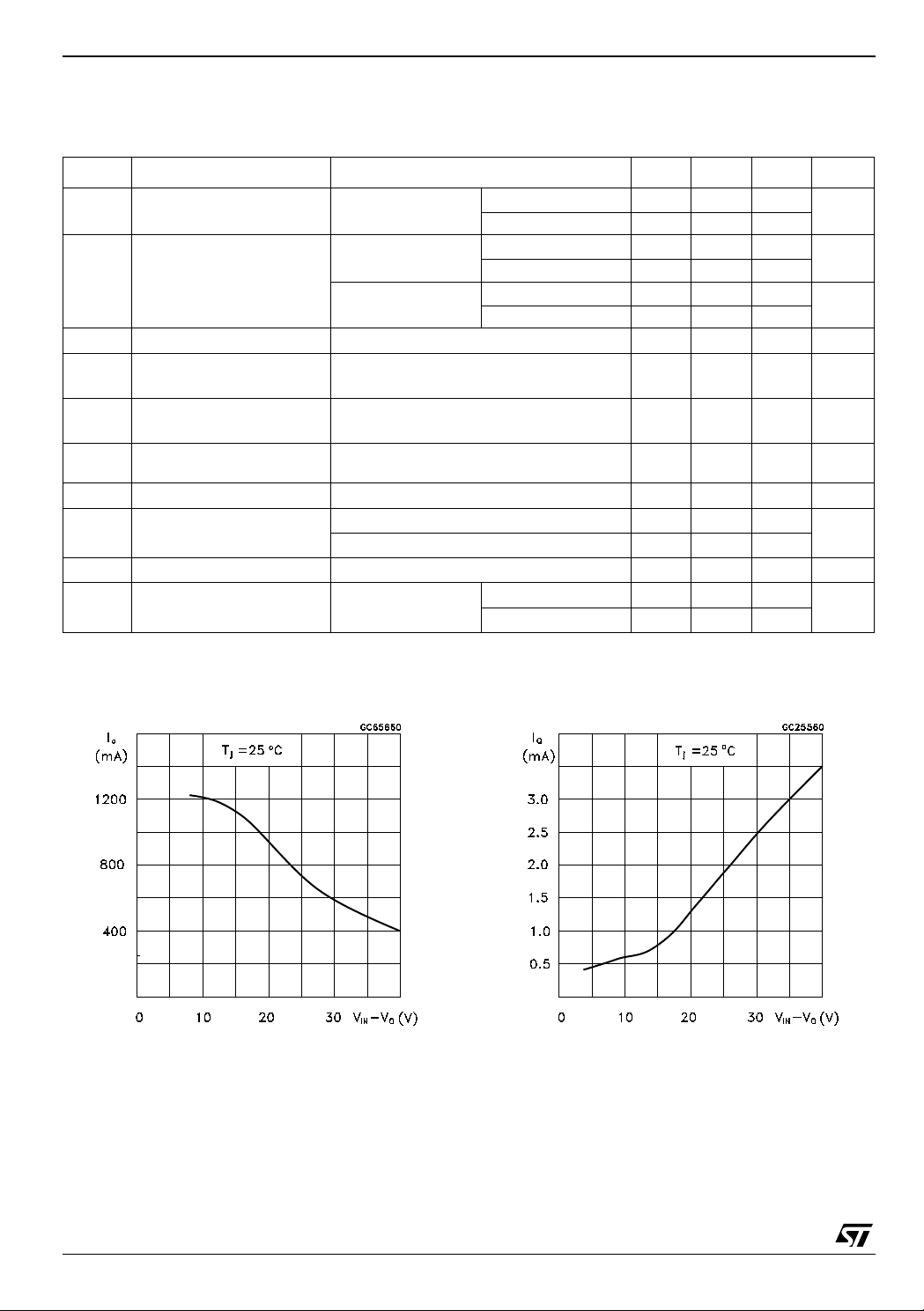
Figure 4: Current Limit
Figure 5: Minimum Operating Current
4/13
Page 5

APPLICATION INFORMATION
The LM317L provides an internal reference
voltage of 1.25V between the output and
adjustments terminals. This is used to set a
constant current flow across an external resistor
divider (see fig. 4), giving an output voltage V
V
O
= V
(1 + R2/R1) + I
REF
ADJ R2
of:
O
The device was designed to minimize the term
I
(100µA max) and to maintain it very constant
ADJ
with line and load changes. Usually, the error term
I
× R2 can be neglected. To obtain the previous
ADJ
requirement, all the regulator quiescent current is
returned to the output terminal, imposing a
minimum load current condition. If the load is
insufficient, the output voltage will rise.
Figure 6: Basic Adjustable Regulator
LM217L/LM317L
Since the LM317L is a floating regulator and
"sees" only the input-to-output differential voltage,
supplies of very high voltage with respect to
ground can be regulated as long as the maximum
input-to-output differential is not exceeded.
Furthermore, programmable regulator are easily
obtainable and, by connecting a fixed resistor
between the adjustment and output, the device
can be used as a prec ision current regulator. In
order to optim ize the load regulation, the current
set resistor R
as possible to the regulator, while the ground
terminal of R
load to provide remote ground sensing.
(see fig. 4) should be tied as close
1
should be near the ground of the
2
Figure 7: Voltage Regulator with Protection Diodes
5/13
Page 6
LM217L/LM317L
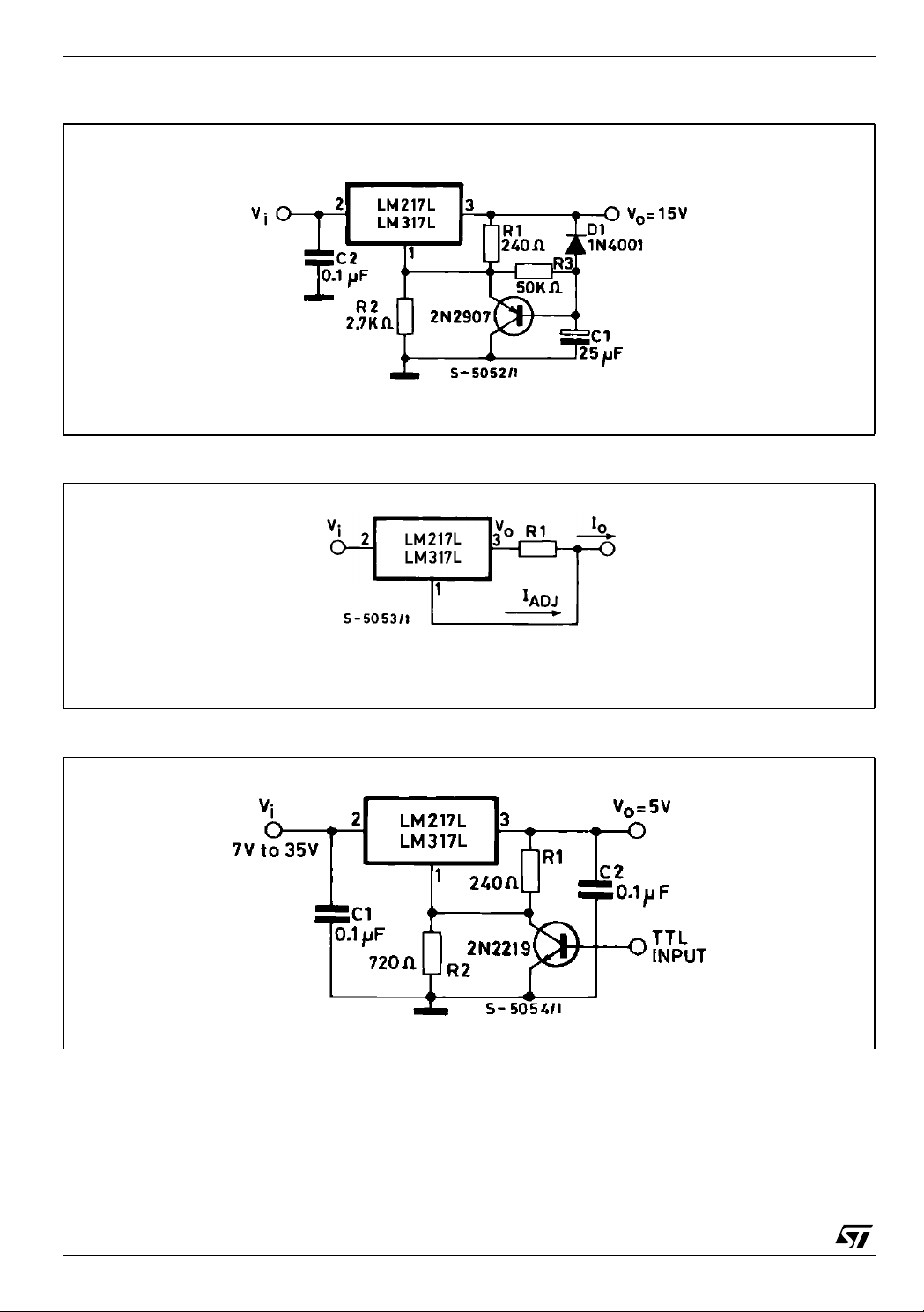
Figure 8: Slow Turn-on 15V R egulato r
Figure 9: Curr ent Regulator
V
ref
IO = + I
R
1
ADJ
1.25V
≈
R
Figure 10: 5V Ele ctronic S hut-down R egulator
1
6/13
Page 7

Figure 11: Digitally Selected Outputs
(R2 = sets maximum VO)
LM217L/LM317L
7/13
Page 8
LM217L/LM317L
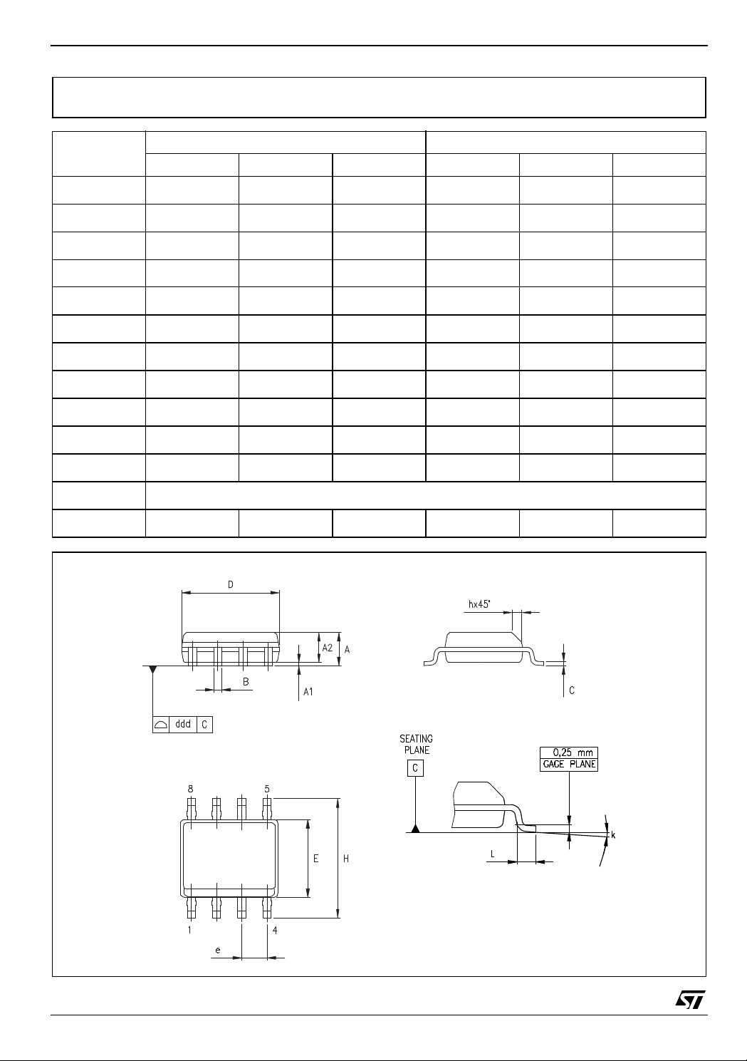
SO-8 MECHANICAL DATA
DIM.
A 1.35 1.75 0.053 0.069
A1 0.10 0.25 0.04 0.010
A2 1.10 1.65 0.043 0.065
B 0.33 0.51 0.013 0.020
C 0.19 0.25 0.007 0.010
D 4.80 5.00 0.189 0.197
E 3.80 4.00 0.150 0.157
e 1.27 0.050
H 5.80 6.20 0.228 0.244
h 0.25 0.50 0.010 0.020
L 0.40 1.27 0.016 0.050
k ˚ (max.)
ddd 0.1 0.04
MIN. TYP MAX. MIN. TYP. MAX.
mm. inch
8
8/13
0016023/C
Page 9

LM217L/LM317L
TO-92 MECHANICA DATA
mm. mils
DIM.
MIN. TYP MAX. MIN. TYP. MAX.
A 4.32 4.95 170.1 194.9
b 0.36 0.51 14.2 20.1
D 4.45 4.95 175.2 194.9
E 3.30 3.94 129.9 155.1
e 2.41 2.67 94.9 105.1
e1 1.14 1.40 44.9 55.1
L 12.7 15.49 500.0 609.8
R 2.16 2.41 85.0 94.9
S1 0.92 1.52 36.2 59.8
W 0.41 0.56 16.1 22.0
0102782/C
9/13
Page 10
LM217L/LM317L
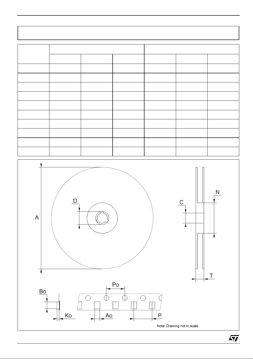
Tape & Reel SO-8 MECHANICAL DATA
mm. inch
DIM.
MIN. TYP MAX. MIN. TYP. MAX.
A 330 12.992
C 12.8 13.2 0.504 0.519
D 20.2 0.795
N 60 2.362
T 22.4 0.882
Ao 8.1 8.5 0.319 0.335
Bo 5.5 5.9 0.216 0.232
Ko 2.1 2.3 0.082 0.090
Po 3.9 4.1 0.153 0.161
P 7.9 8.1 0.311 0.319
10/13
Page 11
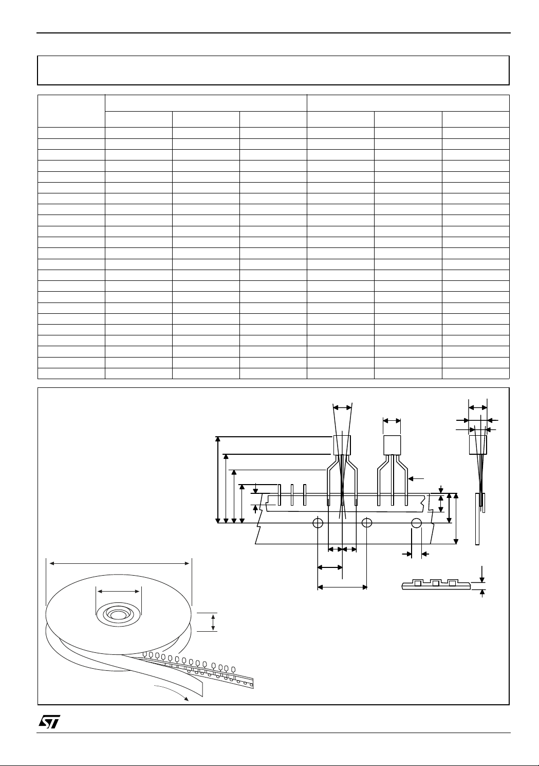
Tape & Reel for TO-92 MECHANICAL DATA
LM217L/LM317L
DIM.
MIN. TYP MAX. MIN. TYP. MAX.
mm. inch
A1 4.80 0.189
T 3.80 0.150
T1 1.60 0.063
T2 2.30 0.091
d 0.48 0.019
P0 12.5 12.9 0.492 0.508
P2 5.65 7.05 0.222 0.278
F1, F2 2.44 2.54 2.94 0.096 0.100 0.116
delta H ±2 0.079
W 17.5 18.00 19.0 0.689 0.709 0.748
W0 5.7 6.3 0.224 0.248
W1 8.5 9.25 0.335 0.364
W2 0.50 0.20
H 18.50 18.70 0.728 0.726
H0 15.50 16.50 0.610 0.650
H1 25.00 0.984
D0 3.8 4.2 0.150 0.165
t 0.90 0.035
L1 3 0.118
delta P ±1 0.039
u 50 1.968
Φ1 360 14.173
Φ2 30 1.181
H1
delta P
A1
delta H
H
H0
L
d
W2
T
T2
T1
Φ1
Φ2
Pull-out direction
l1
W
W0
W1
F1
F2
P2
P0
D0
t
u
DRAWING NOT IN SCALE
11/13
Page 12

LM217L/LM317L
Table 5: Revision History
Date R evisio n Descrip tion of Change s
16-Mar-2005 2 Add Tape & Reel for TO-92.
12/13
Page 13

LM217L/LM317L
Information furnished is believed to be accurate and reliable. However, STMicroelectronics assumes no responsibility for the consequences
of use of such information nor for any infringement of patents or other rights of third parties which may result from its use. No license is granted
by implic ati o n or ot h er wis e und er an y pat ent or pa te nt r igh ts of STMi cr oe l ect ro ni cs . Sp ec if i cat i on s ment i o ned i n th is p ub li c ati on ar e s ubj ec t
to change without notice. This publication supersedes and replaces all information previously supplied. STMicroelectr onics products are not
authorized for use as critical components in life support devices or systems without express written approval of STMicroelectronics.
The ST logo is a registered trademark of STMicroelectronics
All other names are the property of their respective owners
© 2005 STMicroelectronics - All Rights Reserved
STMicroelectronics group of companies
Australia - Belgium - Brazil - Canada - China - Czech Republic - Finland - France - Germany - Hong Kong - India - Israel - Italy - Japan -
Malaysia - Malta - Morocco - Singapore - Spain - Sweden - Switzerland - United Kingdom - United States of America
www.st.com
13/13
 Loading...