

Page 1

LM217, LM317
TO-220
TO-220FP
D²PAK
1.2 V to 37 V adjustable voltage regulators
Datasheet - production data
Description
The LM217, LM317 are monolithic integrated
circuits in TO-220, TO-220FP and D²PAK
packages intended for use as positive adjustable
voltage regulators. They are designed to supply
more than 1.5 A of load current with an output
voltage adjustable over a 1.2 to 37 V range. The
nominal output voltage is selected by means of a
resistive divider, making the device exceptionally
easy to use and eliminating the stocking of many
fixed regulators.
Features
• Output voltage range: 1.2 to 37 V
• Output current in excess of 1.5 A
• 0.1 % line and load regulation
• Floating operation for high voltages
• Complete ser ies of protecti ons: current limit ing,
thermal shutdown and SOA control
Table 1. Device summary
Order codes
TO-220 (single gauge) TO-220 (double gauge) D²PAK (tape and reel) TO-220FP
LM217T LM217T-DG LM217D2T-TR
LM317T LM317T-DG LM317D2T-TR LM317P
LM317BT
March 2014 DocID2154 Rev 19 1/25
This is information on a product in full production.
www.st.com
Page 2

Contents LM217, LM317
Contents
1 Pin configuration . . . . . . . . . . . . . . . . . . . . . . . . . . . . . . . . . . . . . . . . . . . 3
2 Maximum ratings . . . . . . . . . . . . . . . . . . . . . . . . . . . . . . . . . . . . . . . . . . . . 4
3 Diagram . . . . . . . . . . . . . . . . . . . . . . . . . . . . . . . . . . . . . . . . . . . . . . . . . . . 5
4 Electrical characteristics . . . . . . . . . . . . . . . . . . . . . . . . . . . . . . . . . . . . . 6
5 Typical characteristics . . . . . . . . . . . . . . . . . . . . . . . . . . . . . . . . . . . . . . . 9
6 Application information . . . . . . . . . . . . . . . . . . . . . . . . . . . . . . . . . . . . . 10
7 Package mechanical data . . . . . . . . . . . . . . . . . . . . . . . . . . . . . . . . . . . . 14
8 Packaging mechanical data . . . . . . . . . . . . . . . . . . . . . . . . . . . . . . . . . . 22
9 Revision history . . . . . . . . . . . . . . . . . . . . . . . . . . . . . . . . . . . . . . . . . . . 24
2/25 DocID2154 Rev 19
Page 3
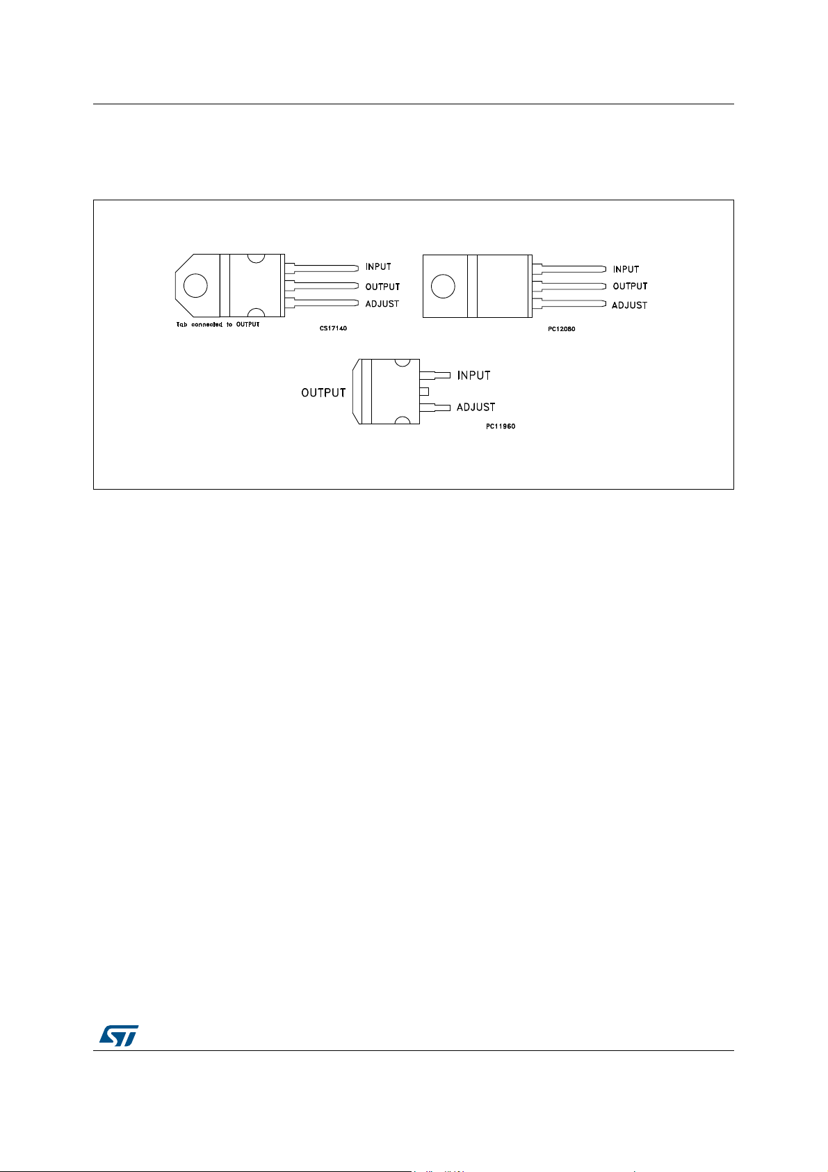
LM217, LM317 Pin configuration
72)3
72
'ð3$.
1 Pin configuration
Figure 1. Pin connections (top view)
DocID2154 Rev 19 3/25
25
Page 4
Maximum ratings LM217, LM317
2 Maximum ratings
Table 2. Absolute maximum ratings
Symbol Parameter Value Unit
- VOInput-reference differential voltage 40 V
V
I
I
Output current Internally limited A
O
LM217 - 25 to 150
°C
T
OP
Operating junction temperature for:
LM317 0 to 125
LM317B -40 to 125
T
P
STG
Power dissipation Internally limited
D
Storage temperature - 65 to 150 °C
Note: Absolute maximum ratings are those values beyond which damage to the device may occur.
Functional operation under these condition is not implied.
Table 3. Thermal data
Symbol Parameter D²PAK TO-220 TO-220FP Unit
R
R
thJC
thJA
Thermal resistance junction-case 3 5 5 °C/W
Thermal resistance junction-ambient 62.5 50 60 °C/W
4/25 DocID2154 Rev 19
Page 5
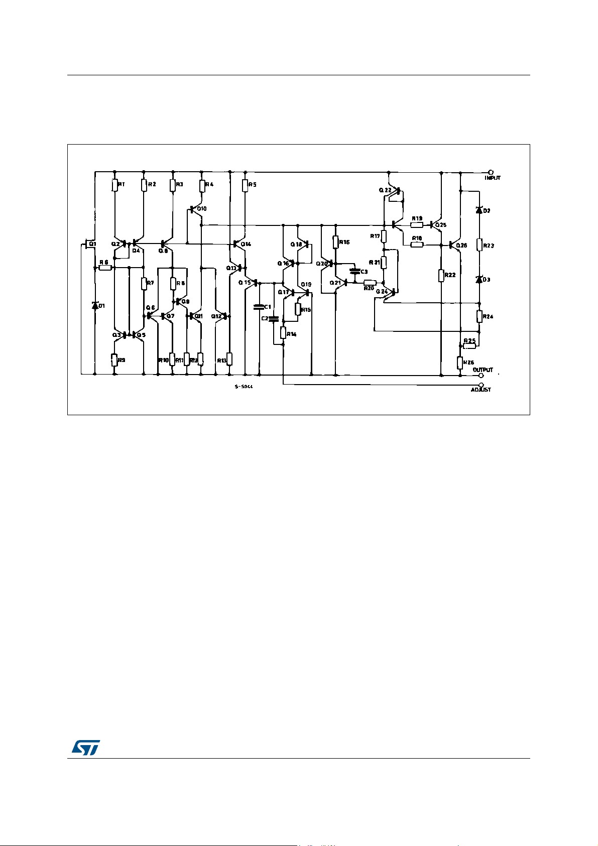
LM217, LM317 Diagram
3 Diagram
Figure 2. Schematic diagram
DocID2154 Rev 19 5/25
25
Page 6

Electrical characteristics LM217, LM317
4 Electrical characteristics
VI - VO = 5 V, IO = 500 mA, I
= 1.5 A and P
MAX
= 20 W, TJ = - 55 to 150 °C, unless
MAX
otherwise specified.
Symbol Parameter Test conditions Min. Typ. Max. Unit
ΔV
ΔV
I
ΔI
V
ΔV
I
O(min)
I
O(max)
Line regulation VI - VO = 3 to 40 V
O
Load regulation
O
Adjustment pin current 50 100 µA
ADJ
Adjustment pin current VI - VO = 2.5 to 40V IO = 10 mA to I
ADJ
Reference voltage
REF
Output voltage
O/VO
temperature stabil ity
Minimum load curre nt VI - VO = 40 V 3.5 5 mA
Maximum load current
Output noise voltage
eN
(percentage of V
SVR Supply voltage rejection
1. C
is connected between adjust pin and ground.
ADJ
Table 4. Electrical characteristics for LM217
T
= 25°C 0.01 0.02
J
≤5 V
V
O
I
= 10 mA to I
O
≥5 V,
V
O
= 10 mA to I
I
O
- VO = 2.5 to 40V IO= 10 mA to I
V
I
PD ≤ P
MAX
V
- VO ≤ 15 V, PD < P
I
- VO = 40 V, PD < P
V
I
)
O
B = 10Hz to 100kHz, T
(1)
TJ = 25°C, f = 120Hz
MAX
MAX
TJ = 25°C 5 15
TJ = 25°C 0.1 0.3
MAX
, TJ = 25°C 0.4
MAX
= 25°C 0.003 %
J
C
=0 65
ADJ
=10µF 66 80
C
ADJ
MAX
MAX
0.02 0.05
%/V
20 50
0.3 1
0.2 5 µA
1.2 1.25 1.3 V
1%
1.5 2.2
mV
%
A
dB
6/25 DocID2154 Rev 19
Page 7
LM217, LM317 Electrical characteristics
VI - VO = 5 V, IO = 500 mA, I
= 1.5 A and P
MAX
= 20 W, TJ = 0 to 125 °C, unless
MAX
otherwise specified.
Symbol Parameter Test conditions Min. Typ. Max. Unit
ΔV
ΔV
I
ΔI
V
ΔV
I
O(min)
I
O(max)
Line regulation VI - VO = 3 to 40 V
O
Load regulation
O
Adjustment pin current 50 100 µA
ADJ
Adjustment pin current
ADJ
Reference voltage
REF
(between pin 3 and pin 1)
Output voltage
O/VO
temperature stabil ity
Minimum load curre nt VI - VO = 40 V 3.5 10 mA
Maximum load current
Output noise voltage
eN
(percentage of V
SVR Supply voltage rejection
1. C
is connected between adjust pin and ground.
ADJ
Table 5. Electrical characteristics for LM317
T
= 25°C 0.01 0.04
J
V
≤ 5 V
O
= 10 mA to I
I
O
≥5 V,
V
O
I
= 10 mA to I
O
MAX
MAX
VI - VO = 2.5 to 40V,
I
= 10 mA to 500mA
O
VI - VO = 2.5 to 40V IO = 10 mA to 500mA
≤ P
P
D
MAX
V
- VO ≤ 15 V, PD < P
I
- VO = 40 V, PD < P
V
I
)
O
B = 10Hz to 100kHz, TJ = 25°C 0.003 %
(1)
TJ = 25°C, f = 120Hz
TJ = 25°C 5 25
TJ = 25°C 0.1 0.5
MAX
, TJ = 25°C 0.4
MAX
C
=0 65
ADJ
=10µF 66 80
C
ADJ
0.02 0.07
%/V
20 70
0.3 1.5
0.2 5 µA
1.2 1.25 1.3 V
1%
1.5 2.2
mV
%
A
dB
DocID2154 Rev 19 7/25
25
Page 8

Electrical characteristics LM217, LM317
VI - VO = 5 V, IO = 500 mA, I
= 1.5 A and P
MAX
= 20 W, TJ = - 40 to 125 °C, unless
MAX
otherwise specified.
Symbol Parameter Test conditions Min. Typ. Max. Unit
ΔV
ΔV
I
ΔI
V
ΔV
I
O(min)
I
O(max)
Line regulation VI - VO = 3 to 40 V
O
Load regulation
O
Adjustment pin current 50 100 µA
ADJ
Adjustment pin current
ADJ
Reference voltage
REF
(between pin 3 and pin 1)
Output voltage
O/VO
temperature stability
Minimum load cu rrent VI - VO = 40 V 3.5 10 mA
Maximum load current
Output noise voltage
eN
(percentage of V
SVR Suppl y vol tage rejection
1. C
is connected between adjust pin and ground.
ADJ
T able 6. Electrical characteristics for LM317B
T
= 25°C 0.01 0.04
J
V
≤ 5 V
O
= 10 mA to I
I
O
≥5 V,
V
O
I
= 10 mA to I
O
MAX
MAX
VI - VO = 2.5 to 40V,
I
= 10 mA to 500mA
O
VI - VO = 2.5 to 40V IO = 10 mA to 500mA
≤ P
P
D
MAX
V
- VO ≤ 15 V, PD < P
I
- VO = 40 V, PD < P
V
I
)
O
B = 10Hz to 100kHz, TJ = 25°C 0.003 %
(1)
TJ = 25°C, f = 120Hz
TJ = 25°C 5 25
TJ = 25°C 0.1 0.5
MAX
, TJ = 25°C 0.4
MAX
C
=0 65
ADJ
=10µF 66 80
C
ADJ
0.02 0.07
%/V
20 70
0.3 1.5
0.25µA
1.2 1.25 1.3 V
1%
1.5 2.2
mV
%
A
dB
8/25 DocID2154 Rev 19
Page 9

LM217, LM317 Typical characteristics
,QSXW,QSXW
2XWSXW2XWSXW
$GM$GM
5 Typical characteristics
Figure 3. Output current vs. input-output
Figure 5. Reference voltage vs. junction
differential voltage
Figure 4. Dropout voltage vs. junction
temperature
Figure 6. Basic adjustable regulator
DocID2154 Rev 19 9/25
25
Page 10

Application information LM217, LM317
**OQVUOQVU
0VUQVUVUQVU
"EKVTUEKVTU
6 Application information
The LM217, LM317 provides an internal reference voltage of 1.25 V between the output and
adjustments terminals. This is used to set a constant current flow across an external resistor
divider (see Figure 6), giving an output voltage V
V
O
= V
(1 + R2/R1) + I
REF
ADJ R2
The device was designed to minimize the term I
constant with line and load changes. Usually, the error term I
obtain the previous requirement, all the regulator quiescent current is returned to the output
terminal, imposing a minimum load current condition. If the load is insufficient, the output
voltage will rise. Since the LM217, LM317 is a floating regulator and "sees" only the input-tooutput differential voltage, supplies of very high voltage with respect to ground can be
regulated as long as the maximum input-to-output differential is not exceeded. Furthermore,
programmable regulators are easily obtainable and, by connecting a fixed resistor between
the adjust men t a n d ou t pu t , th e de vi ce ca n be us ed a s a precision cu rr e n t r e gulator. In or de r
to optimize the load regulation, the current set resistor R
close as possible to the regulator, while the ground terminal of R
of the load to provide remote ground sensing. Performance may be improved with added
capacitance as follow:
• An input bypass capacitor of 0.1 µF
• An adjustment terminal to ground 10 µF capacitor to improve the ripple rejection of
about 15 dB (C
ADJ
).
• An 1 µF tantalum (or 25 µF Aluminium electrolytic) capacitor on the output to improve
transient response. In addition to external capacitors, it is good practice to add
protection diodes, as shown in Figure 7 D1 protect the device against input short
circuit, while D2 protect against output short circuit for capacitance discharging.
of:
O
(100 µA max) and to maintain it very
ADJ
1
× R2 can be neglected. To
ADJ
(see Figure 6) should be tied as
should be near the ground
2
Figure 7. Voltage regulator with protection diodes
Note: D1 protect the device against input short circuit, while D2 protects against output short
circuit for capacitors discharging.
10/25 DocID2154 Rev 19
Page 11

LM217, LM317 Application information
**OQVUOQVU
0VUQVUVUQVU
"EKVTUEKVTU
**OQVUOQVU
0VUQVUVUQVU
"EKVTUEKVTU
**OQVUOQVU
0VUQVUVUQVU
"EKVTUEKVTU
Figure 8. Slow turn-on 15 V regulator
Figure 9. Current regulator
IO = (V
/ R1) + I
REF
= 1.25 V / R
ADJ
1
Figure 10. 5 V electronic shut-down regulator
DocID2154 Rev 19 11/25
25
Page 12

Application information LM217, LM317
**OQVUOQVU
0VUQVUVUQVU
"EKVTUEKVTU
**OQVUOQVU
0VUQVUVUQVU
"EKVTUEKVTU
Figure 11. Digitally selected outputs
(R2 sets maximum VO)
Figure 12. Battery charger (12 V)
* RS sets output impedance of charger ZO = RS (1 + R2/R1). Use of RS allows low charging rates whit fully
charged battery.
12/25 DocID2154 Rev 19
Page 13

LM217, LM317 Application information
**OQVUOQVU
0VUQVUVUQVU
"EKVTUEKVTU
* R3 sets peak current (0.6 A for 1 0).
** C1 recommended to filter out input transients.
Figure 13. Current limited 6 V charger
DocID2154 Rev 19 13/25
25
Page 14

Package mechanical data LM217, LM317
BUHY'
7 Package mechanical data
In order to meet environmental requirements, ST offers these devices in different grades of
®
ECOPACK
specifications, grade definitions and product status are available at: www.st.com.
ECOPACK
packages, depending on their level of environmental compliance. ECOPACK®
®
is an ST trademark.
Figure 14. TO-220 (single gauge) drawing
14/25 DocID2154 Rev 19
Page 15

LM217, LM317 Package mechanical data
Table 7. TO-220 (single gauge) mechanical data
mm
Dim.
Min. Typ. Max.
A 4.40 4.60
b 0.61 0.88
b1 1.14 1.70
c 0.48 0.70
D 15.25 15.75
E 10 10.40
e 2.40 2.70
e1 4.95 5.15
F 0.51 0.60
H1 6.20 6.60
J1 2.40 2.72
L13 14
L1 3.50 3.93
L20 16.40
L30 28.90
∅
P 3.75 3.85
Q 2.65 2.95
DocID2154 Rev 19 15/25
25
Page 16

Package mechanical data LM217, LM317
BW\SH$B5HYB7
Figure 15. TO-220 (dual gauge) drawing
16/25 DocID2154 Rev 19
Page 17

LM217, LM317 Package mechanical data
Table 8. TO-220 (dual gauge) mechanical data
mm
Dim.
Min. Typ. Max.
A 4.40 4.60
b 0.61 0.88
b1 1.14 1.70
c 0.48 0.70
D 15.25 15.75
D1 1.27
E 10 10.40
e 2.40 2.70
e1 4.95 5.15
F 1.23 1.32
H1 6.20 6.60
J1 2.40 2.72
L13 14
L1 3.50 3.93
L20 16.40
L30 28.90
∅
P 3.75 3.85
Q 2.65 2.95
DocID2154 Rev 19 17/25
25
Page 18

Package mechanical data LM217, LM317
7012510_Rev_K
A
B
H
Dia
L7
D
E
L6
L5
L2
L3
L4
F1
F2
F
G
G1
Figure 16. TO-220FP drawing
18/25 DocID2154 Rev 19
Page 19

LM217, LM317 Package mechanical data
T able 9. TO-220FP mechanical data
mm
Dim.
Min. Typ. Max.
A4.4 4.6
B2.5 2.7
D2.5 2.75
E 0.45 0.7
F0.75 1
F1 1.15 1.70
F2 1.15 1.70
G 4.95 5.2
G1 2.4 2.7
H10 10.4
L2 16
L3 28.6 30.6
L4 9.8 10.6
L5 2.9 3.6
L6 15.9 16.4
L7 9 9.3
Dia 3 3.2
DocID2154 Rev 19 19/25
25
Page 20

Package mechanical data LM217, LM317
0079457_T
Figure 17. D²PAK drawing
20/25 DocID2154 Rev 19
Page 21

LM217, LM317 Package mechanical data
Table 10. D²PAK mechanical data
mm
Dim.
Min. Typ. Max.
A4.40 4.60
A1 0.03 0.23
b0.70 0.93
b2 1.14 1.70
c0.45 0.60
c2 1.23 1.36
D8.95 9.35
D1 7.50
E 10 10.40
E1 8.50
e2.54
e1 4.88 5.28
H 15 15.85
J1 2.49 2.69
L2.29 2.79
L1 1.27 1.40
L2 1.30 1.75
R0.4
V2 0° 8°
DocID2154 Rev 19 21/25
25
Page 22

Packaging mechanical data LM217, LM317
P1
A0
D1
P0
F
W
E
D
B0
K0
T
User direction of feed
P2
10 pitches cumulative
tolerance on tape +/- 0.2 mm
User direction of feed
R
Bending radius
B1
For machine ref. only
including draft and
radii concentric around B0
AM08852v1
Top cover
tape
8 Packaging mechanical data
Figure 18. Tape for D²PAK
22/25 DocID2154 Rev 19
Page 23

LM217, LM317 Packaging mechanical data
A
D
B
Full radius
G measured at hub
C
N
REEL DIMENSIONS
40mm min.
Access hole
At sl ot location
T
Tape slot
in core for
tape start 25 mm min.
width
AM08851v2
Figure 19. Reel for D²PAK
Table 11. D²PAK tape and reel mechanical data
Tape Reel
mm
Dim.
Dim.
Min. Max. Min. Max.
A0 10.5 10.7 A 330
B0 15.7 15.9 B 1.5
D 1.5 1.6 C 12.8 13.2
D1 1.59 1.61 D 20.2
E 1.65 1.85 G 24.4 26.4
F 11.4 11.6 N 100
K0 4.8 5.0 T 30.4
P0 3.9 4.1
P1 11.9 12.1 Base qty 1000
P2 1.9 2.1 Bulk qty 1000
R50
T 0.25 0.35
W 23.7 24.3
mm
DocID2154 Rev 19 23/25
25
Page 24

Revision history LM217, LM317
9 Revision history
Table 12. Document revision history
Date Revision Changes
01-Sep-2004 10 Mistake V
19-Jan-2007 11
13-Jun-2007 12
D²PAK mechanical data has been updated, add footprint data and the
document has been reformatted.
Change values ΔI
= 10 mA to 500 mA on Table 5.
I
O
==> VO, tables 1, 4 and 5.
REF
and V
ADJ
REF
test condition of IO = 10 mA to I
23-Nov-2007 13 Added Table 1.
06-Feb-2008 14
02-Mar-2010 15
17-Nov-2010 16 Modified: R
Added: TO-220 mechanical data Figure 14 on page 14 and Table 6 on
page 13.
Added: notes Figure 14 on page 14, Figure 15 on page 15, Figure 16 and
Figure 17 on page 16.
value for TO-220 Table 3 on page 4.
thJC
18-Nov-2011 17 Added: order code LM317T-DG Ta bl e1 on page 1.
13-Feb-2012 18 Added: order code LM217T-DG Ta bl e1 on page 1.
The part number LM117 has been moved to a separate datasheet.
Removed TO-3 package.
Updated the description in cover page
Modified Table 1: Device summary, Table 3: Thermal data, Figure 1: Pin
12-Mar-2014 19
connections (top view) , Section 4: Electrical characteristics, Section 5: Typical
characteristics, Section 6: Application information, Section 7: Package
mechanical data.
Added Section 8: Packaging mechanical data.
Minor text changes.
MAX
==>
24/25 DocID2154 Rev 19
Page 25

LM217, LM317
Please Read Carefully:
Information in this document i s provided solely in connecti on with ST produ cts. STMicroelec troni cs NV and its subsidiari es (“ST”) res erve the
right to make changes , cor recti ons , modific ati ons or improv eme nts, t o th is doc ument, and the prod uc ts an d serv ices des crib ed he rein a t any
time, without notice.
All ST products are sold pursuant to ST’s terms and conditions of sale.
Purchasers are solely responsible for the choice, selection and use of the ST products and services described herein, and ST assumes no
liability whatsoever relating to the choice, selection or use of the ST products and services des cribed herein.
No license, express or implied, by estoppel or otherwise, to any intellectual property rights is granted under this document. If any part of this
document refers to any third party products or services it shall not be deemed a license grant by ST for the use of such third party products
or services, or any intellectual property contained therein or considered as a warranty covering the use in any manner whatsoever of such
third party products or services or any intellectual property contained therein.
UNLESS OTHERWISE SET FORTH IN ST’S TERMS AND CONDITIONS OF SALE ST DISCLAIMS ANY EXPRESS OR IMPLIED
WARRANTY WITH RESPECT TO THE USE AND/OR SALE OF ST PRODUCTS INCLUDING WITHOUT LIMITATION IMPLIED
WARRANTIES OF MERCHANTABILITY, FITNESS FOR A PARTICULAR PURPOSE (AND THEIR EQUIVALENTS UNDER THE LAWS
OF ANY JURISDICTION), OR INFRINGEMENT OF ANY PATENT, COPYRIGHT OR OTHER INTELLECTUAL PROPERTY RIGHT.
ST PRODUCTS ARE NOT DESIGNED OR AUTHORIZED FOR USE IN: (A) SAFETY CRITICAL APPLICATIONS SUCH AS LIFE
SUPPORTING, ACTIVE IMPLANTED DEVICES OR SYSTEMS WITH PRODUCT FUNCTIONAL SAFETY REQUIREMENTS; (B)
AERONAUTIC APPLICATIONS; (C) AUTOMOTIVE APPLICATIONS OR ENVIRONMENTS, AND/OR (D) AEROSPACE APPLICATIONS
OR ENVIRONMENTS. WHERE ST PRODUCTS ARE NOT DESIGNED FOR SUCH USE, THE PURCHASER SHALL USE PRODUCTS AT
PURCHASER’S SOLE RISK, EVEN IF ST HAS BEEN INFORMED IN WRITING OF SUCH USAGE, UNLESS A PRODUCT IS
EXPRESSLY DESIGNATED BY ST AS BEING INTENDED FOR “AUTOMOTIVE, AUTOMOTIVE SAFETY OR MEDICAL” INDUSTRY
DOMAINS ACCORDING TO ST PRODUCT DESIGN SPECIFICATIONS. PRODUCTS FORMALLY ESCC, QML OR JAN QUALIFIED ARE
DEEMED SUITABLE FOR USE IN AEROSPACE BY THE CORRESPONDING GOVERNMENTAL AGENCY.
Resale of ST products with prov isions differen t from the state ments and/or tec hnical featur es set forth in th is document shall immediatel y void
any warranty granted by ST for the ST product or service described herein and shall not create or extend in any manner whatsoever, any
liability of ST.
ST and the ST logo are trademark s or registered trademarks of ST in various countries.
Information in this document supers edes and replaces all information previously supplied.
The ST logo is a registered trademark of STMicroelectronics. All other names are the property of their respective owners.
© 2014 STMicroelectronics - All rights reserv ed
STMicroelectronics group of companies
Australia - Belgium - Brazil - Canada - China - Czech Republic - Finland - France - Germany - Hong Kong - India - Israel - Italy - Japan -
Malaysia - Malta - Morocco - Philippines - Si ngapore - Spain - Sweden - Switzerland - United Kingdom - United States of America
www.st.com
DocID2154 Rev 19 25/25
25
 Loading...