

Page 1

Features
■ Wide single supply voltage range or dual
supplies +2 V to +36 V or ±1 V to ±18 V
■ Very low supply current (0.4 mA) independent
of supply voltage (1 mW/comparat or at +5 V)
■ Low input bias current: 25 nA typ.
■ Low input offset current: ±5 nA typ.
■ Input common-mode voltage range includes
negative rail
■ Low output saturation voltage:
250 mV typ. (I
■ Differential input voltage range equal to the
supply voltage
■ TTL, DTL, ECL, MOS, CMOS compatible
outputs
= 4 mA)
O
LM2903
Low power dual voltage comparator
N
DIP8
(Plastic package)
D
SO-8
(Plastic micropackage)
Description
This device consists of two independent low
power voltage comparators designed specifically
to operate from a single supply over a wide range
of voltages. Oper ation from split pow er supplies is
also possible.
These comparators also have a unique
characteristic: the input common-mode voltage
range includes the negative rail even though
operated from a single power supply voltage.
P
TSSOP8
(Thin shrink small outline package)
Pin connections (top view)
February 2008 Rev 7 1/14
www.st.com
14
Page 2

Schematic diagram LM2903
1 Schematic diagram
Figure 1. Schematic diagram (1/2 LM2903)
VCC+
3.5µA 100µA 3.5µA 100µA
Non-Inverting
Input
Inverting
Input
Vo
VCC- VCC-
VCC-
2/14
Page 3

LM2903 Absolute maximum ratings and operating conditions
2 Absolute maximum ratings and operating conditions
Table 1. Absolute maximum ratings
Symbol Parameter Value Unit
V
CC
V
id
V
in
R
thja
R
thjc
T
j
T
stg
ESD
1. Short-circuits from the output to V
maximum output current is approximately 20 mA, independent of the magnitude of V
2. Short-circuits can cause excessive heating and destructive dissipation. Values are typical.
3. Human body model: A 100 pF capacitor is charged to the specified voltage, then discharged through a
1.5 kΩ resistor between two pins of the device. This is done for all couples of connected pin combinations
while the other pins are floating.
4. Machine model: A 200pF capacitor is charged to the specified voltage, then discharged directly between
two pins of the device with no external series resistor (internal resistor < 5 Ω). This is done for all couples of
connected pin combinations while the other pins are floating.
5. Charged device model: all pins and the package are charged together to the specified voltage and then
discharged directly to the ground through only one pin. This is done for all pins.
Table 2. Operating conditions
Supply voltage ±18 to 36 V
Differential input voltage ±36 V
Input voltage -0.3 to +36 V
Output short-circuit to ground
(1)
Thermal resistance junction to ambient
DIP8
SO-8
TSSOP8
Thermal resistance junction to case
(2)
DIP8
SO-8
TSSOP8
(2)
Infinite
85
125
120
41
40
37
°C/W
°C/W
Maximum junction temperature +150 °C
Storage temperature range -65 to +150 °C
Human body model (HBM)
Machine model (MM)
CDM: charged device model
CC
(3)
(4)
(5)
+
can cause excessive heating and possible destruction. The
800 V
200 V
1.5 kV
+
.
CC
Symbol Parameter Value Unit
V
T
icm
oper
Common mode input voltage range
≤ T
T
min
amb
≤ T
max
0 to V
0 to V
Operating free-air temperature range -40 to +125 °C
CC
CC
+
-1.5
+
-2
V
3/14
Page 4

Electrical characteristics LM2903
3 Electrical characteristics
Table 3. V
CC
+
= 5V, V
Symbol Parameter Min. Typ. Max. Unit
V
I
I
A
Input offset voltage
io
≤ T
T
min
Input offset current
io
≤ T
T
min
Input bias current
ib
T
≤ T
min
Large signal voltage gain
vd
= 15V, RL=15kΩ, Vo=1 to 11V
V
CC
amb
amb
amb
Supply current (all comparators)
I
V
V
I
I
sink
t
CC
id
OL
OH
res
= 5V, no load
V
CC
= 30V, no load
V
CC
Differential input voltage
Low level output voltage (Vid = -1V, I
≤ T
T
min
amb
High level output current (V
≤ T
T
min
amb
≤ T
Output sink current (Vid = -1V, Vo = 1.5V) 6 16 mA
Small signal response time
Large signal response time
rel
TTL input (V
Output signal at 50% of final value
t
Output signal at 95% of final value
1. At output switch point, VO ≈ 1.4 V, RS = 0 Ω with V
2. The direction of the input current is out of the IC due to the PNP input stage. This current is essentially constant,
3. Positive excursions of input voltage may exceed the power supply level. As long as the other voltage remains within the
4. The response time specified is for a 100 mV input step with 5 mV overdrive.
5. Maximum values are guaranteed by design and evaluation.
+
to V
–1.5 V).
CC
independent of the state of the output, so no loading charge exists on the reference of input lines.
common-mode range, the comparator will provide a proper output state. The low input voltage state must not be less than
–0.3 V (or 0.3 V below the negative power supply, if used).
-
= GND, T
CC
(1)
≤ T
max
≤ T
max
(2)
≤ T
max
≤ T
max
max
= +1.4 V, RL=5.1kΩ to V
ref
amb
(3)
CC =Vo
(4)
(RL = 5.1kΩ to V
(5)
= 25°C (unless otherwise specified)
17
550
25 250
25 200 V/mV
0.4
1
= 4mA)
sink
=30V, Vid = 1V)
+
)1.3µs
CC
+
)
CC
+
from 5 V to 30 V, and over the full input common-mode range (0 V
CC
250 400
0.1
150
400
2.5
V
700
500
15
CC
mV
nA
nA
1
+
mA
V
mV
nA
1
µA
ns
1
µs
4/14
Page 5

LM2903 Electrical characteristics
Figure 2. Supply current vs. supply voltage Figure 3. Input current vs. supply voltage
Figure 4. Output saturation voltage vs.
output current
Figure 5. Response time for various input
overdrives - negative transition
Figure 6. Response time for various input
overdrives - positive transition
5/14
Page 6
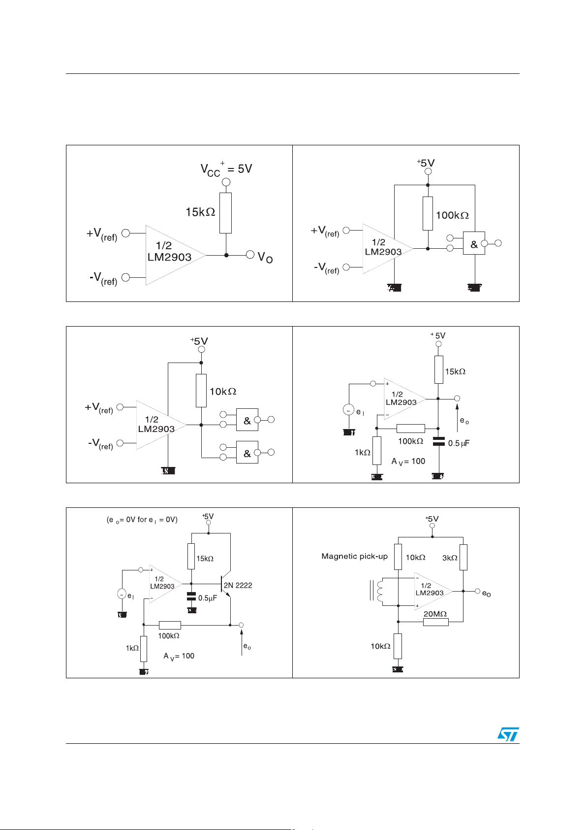
Typical application schematics LM2903
4 Typical application schematics
Figure 7. Basic comparator Figure 8. Driving CMOS
Figure 9. Driving TTL Figure 10. Low frequency op-amp
Figure 11. Low frequency op-amp Figure 12. Transducer amplifier
6/14
Page 7
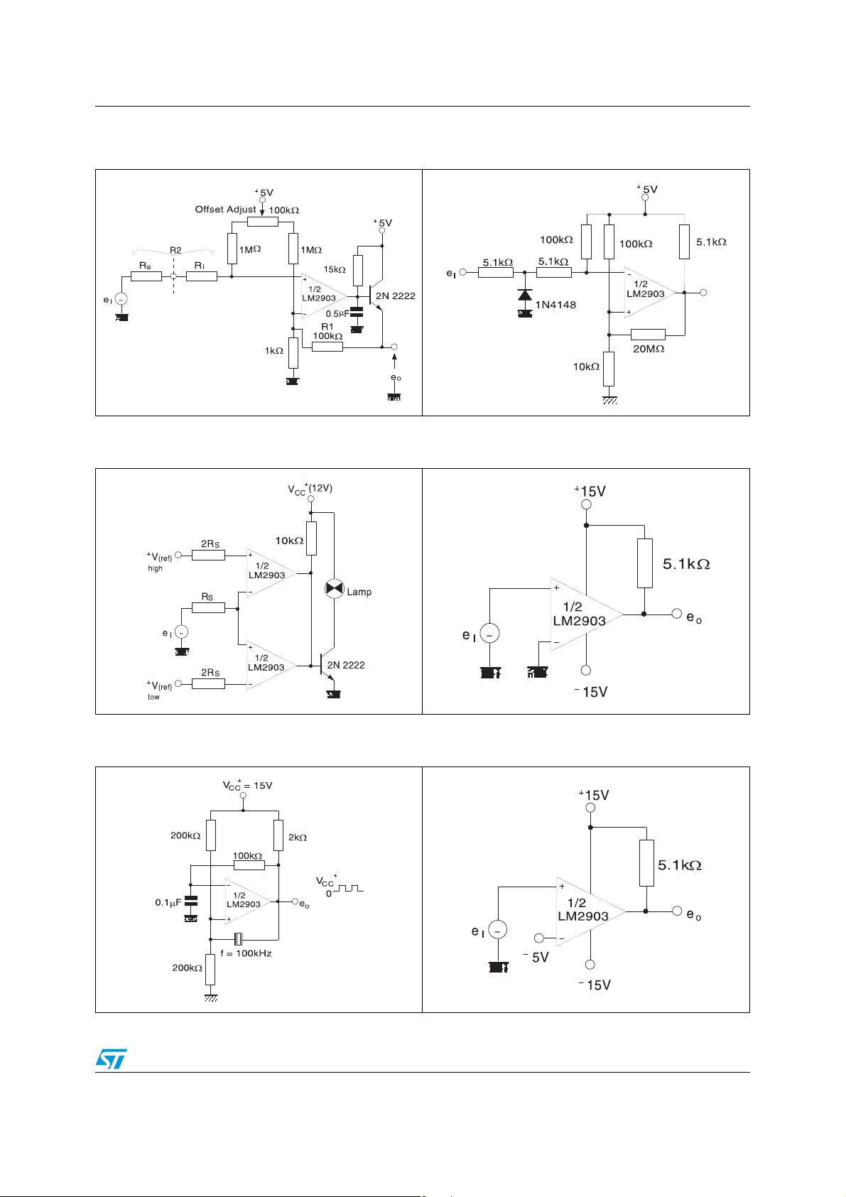
LM2903 Typical application schematics
Figure 13. Low frequency op- amp with offset
adjust
Figure 14. Zero crossing detector (single
power supply)
Figure 15. Limit comparator Figure 16. Split-supply applications - zero
crossing detector
Figure 17. Split-supply applications - crystal
controlled oscillator
Figure 18. Comparator with a negative
reference
7/14
Page 8

Typical application schematics LM2903
Figure 19. Two-decade high-frequency VCO
8/14
Page 9

LM2903 Package information
5 Package information
In order to meet environmental requirements, STMicroelectronics offers these devices in
ECOPACK
category of second level interconnect is marke d on the pa ckage and on the inner box label,
in compliance with JEDEC Standard JESD97. The maximum ratings related t o soldering
conditions are also marked on the inner box label. ECOPACK is an STMicroelectronics
trademark. ECOPACK specifications are available at: www.st.com.
®
packages. These packages have a lead-free second level interconnect. The
9/14
Page 10
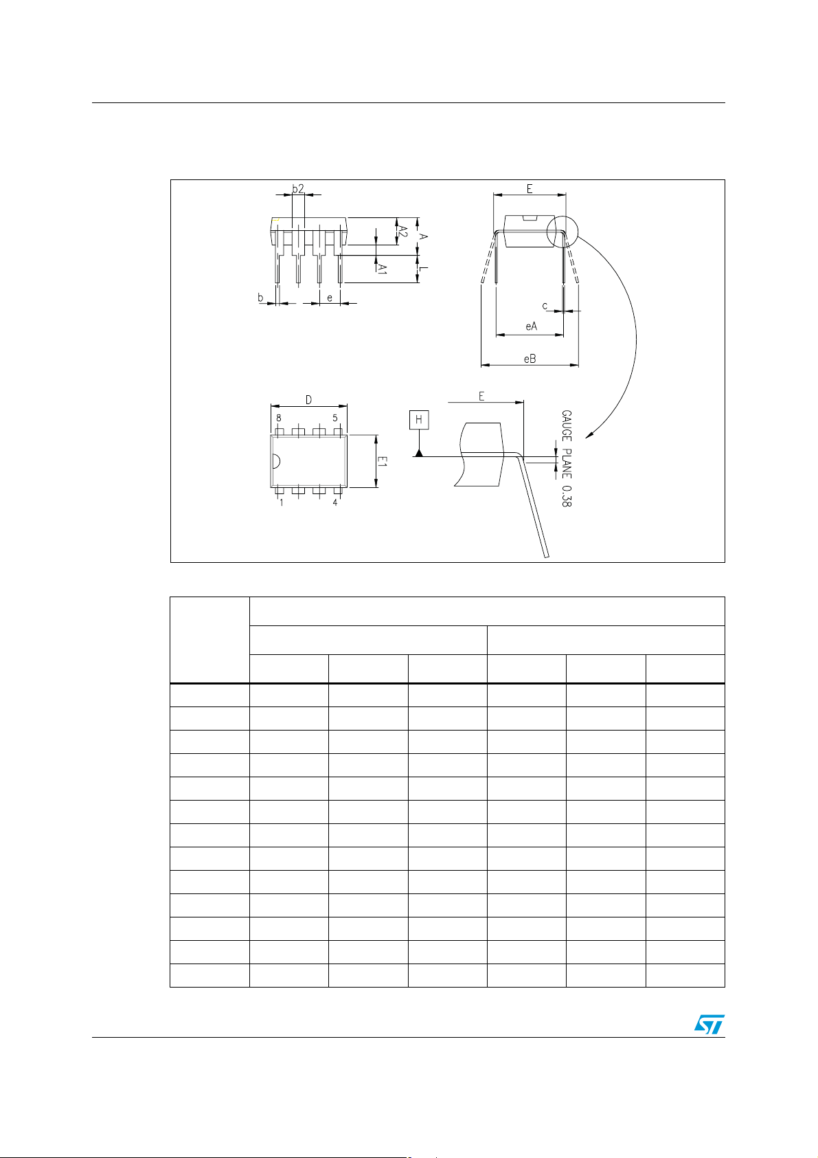
Package information LM2903
5.1 DIP8 package information
Figure 20. DIP8 package mechanical drawing
Table 4. DIP8 package mechanical data
Dimensions
Ref.
Min. Typ. Max. Min. Typ. Max.
A5.330.210
A1 0.38 0.015
A2 2.92 3.30 4.95 0.115 0.130 0.195
b 0.36 0.46 0.56 0.014 0.018 0.022
b2 1.14 1.52 1.78 0.045 0.060 0.070
c 0.20 0.25 0.36 0.008 0.010 0.014
D 9.02 9.27 10.16 0.355 0.365 0.400
E 7.62 7.87 8.26 0.300 0.310 0.325
E1 6.10 6.35 7.11 0.240 0.250 0.280
e 2.54 0.100
eA 7.62 0.300
eB 10.92 0.430
L 2.92 3.30 3.81 0.115 0.130 0.150
Millimeters Inches
10/14
Page 11

LM2903 Package information
5.2 SO-8 package information
Figure 21. SO-8 package mechanical drawing
Table 5. SO-8 package mechanical data
Dimensions
Ref.
Min. Typ. Max. Min. Typ. Max.
A1.750.069
A1 0.10 0.25 0.004 0.010
A2 1.25 0.049
b 0.28 0.48 0.011 0.019
c 0.17 0.23 0.007 0.010
D 4.80 4.90 5.00 0.189 0.193 0.197
E 5.80 6.00 6.20 0.228 0.236 0.244
E1 3.80 3.90 4.00 0.150 0.154 0.157
e 1.27 0.050
h 0.25 0.50 0.010 0.020
L 0.40 1.27 0.016 0.050
k1°8°1°8°
ccc 0.10 0.004
Millimeters Inches
11/14
Page 12

Package information LM2903
5.3 TSSOP8 package information
Figure 22. TSSOP8 package mechanical drawing
Table 6. TSSOP8 package mechanical data
Dimensions
Ref.
Min. Typ. Max. Min. Typ. Max.
A 1.2 0.047
A1 0.05 0.15 0.002 0.006
A2 0.80 1.00 1.05 0.031 0.039 0.041
b 0.19 0.30 0.007 0.012
c 0.09 0.20 0.004 0.008
D 2.90 3.00 3.10 0.114 0.118 0.122
E 6.20 6.40 6.60 0.244 0.252 0.260
E1 4.30 4.40 4.50 0.169 0.173 0.177
e 0.65 0.0256
k0°8°0°8°
L 0.45 0.60 0.75 0.018 0.024 0.030
L1 1 0.039
aaa 0.1 0.004
Millimeters Inches
12/14
Page 13

LM2903 Ordering information
6 Ordering information
Table 7. Order codes
Order code
Temperature
range
LM2903N
LM2903D/DT SO-8 Tube or tape & reel
LM2903PT TSSOP8 Tape & reel
LM2903YD
LM2903YDT
LM2903YPT
1. Qualified and characterized according to AEC Q100 and Q003 or equivalent, advanced screening
according to AEC Q001 & Q 002 or equivalent.
2. Qualification and characterization according to AEC Q100 and Q003 or equivalent, advanced screening
according to AEC Q001 & Q 002 or equivalent are on-going.
(1)
(1)
(2)
-40°C to +125°C
7 Revision history
Table 8. Document revision history
Date Re vision Changes
Package Packing Marking
DIP8 Tube LM2903N
SO-8
(Automotive grade)
TSSOP8
(Automotive grade)
Tube or tape & reel
Tape & reel
2903
2903Y
15-Jun-2003 1 Initial release.
2-May-2005 2 PPAP references inserted in the datasheet see table order code p1.
Electrical characteristics table corrected (see Table 3 on page 4).
8-Aug-2005 3
Pin connections diagram moved to cover page.
Lead-free package information added.
27-Oct-2005 4 PPAP part number added in Table 7: Order codes.
11-May-2007 5
ESD tolerance added in Table 1: Absolute maximum ratings on
page 3.
Added R
thja
and R
, and ESD CDM parameters in Table 1:
thjc
Absolute maximum ratings.
17-Jan-2008 6
Removed V
from electrical characteristics in Table 3.
icm
Reformatted package information in Section 5.
Added footnotes for automotive grade parts in Table 7: Order codes.
Corrected SO-8 package mec hanical data. Dimension E in drawing
21-Feb-2008 7
was marked H in table.
Corrected revision history (revision 6 is of January 2008, not January
2007).
13/14
Page 14

LM2903
Please Read Carefully:
Information in this document is provided solely in connection with ST products. STMicroelectronics NV and its subsidiaries (“ST”) reserve the
right to make changes, corrections, modifications or improvements, to this document, and the products and services described herein at any
time, without notice.
All ST products are sold pursuant to ST’s terms and conditions of sale.
Purchasers are solely res ponsibl e fo r the c hoic e, se lecti on an d use o f the S T prod ucts and s ervi ces d escr ibed he rein , and ST as sumes no
liability whatsoever relati ng to the choice, selection or use of the ST products and services described herein.
No license, express or implied, by estoppel or otherwise, to any intellectual property rights is granted under this document. If any part of this
document refers to any third pa rty p ro duc ts or se rv ices it sh all n ot be deem ed a lice ns e gr ant by ST fo r t he use of su ch thi r d party products
or services, or any intellectua l property c ontained the rein or consi dered as a warr anty coverin g the use in any manner whats oever of suc h
third party products or servi ces or any intellectual property contained therein.
UNLESS OTHERWISE SET FORTH IN ST’S TERMS AND CONDITIONS OF SALE ST DISCLAIMS ANY EXPRESS OR IMPLIED
WARRANTY WITH RESPECT TO THE USE AND/OR SALE OF ST PRODUCTS INCLUDING WITHOUT LIMITATION IMPLIED
WARRANTIES OF MERCHANTABILITY, FITNESS FOR A PARTICUL AR PURPOS E (AND THEIR EQUIVALE NTS UNDER THE LAWS
OF ANY JURISDICTION), OR INFRINGEMENT OF ANY PATENT, COPYRIGHT OR OTHER INTELLECTUAL PROPERTY RIGHT.
UNLESS EXPRESSLY APPROVED IN WRITING BY AN AUTHORIZED ST REPRESENTATIVE, ST PRODUCTS ARE NOT
RECOMMENDED, AUTHORIZED OR WARRANTED FOR USE IN MILITARY, AIR CRAFT, SPACE, LIFE SAVING, OR LIFE SUSTAINING
APPLICATIONS, NOR IN PRODUCTS OR SYSTEMS WHERE FAILURE OR MALFUNCTION MAY RESULT IN PERSONAL INJ URY,
DEATH, OR SEVERE PROPERTY OR ENVIRONMENTAL DAMAGE. ST PRODUCTS WHICH ARE NOT SPECIFIED AS "AUTOMOTIVE
GRADE" MAY ONLY BE USED IN AUTOMOTIVE APPLICATIONS AT USER’S OWN RISK.
Resale of ST products with provisions different from the statements and/or technical features set forth in this document shall immediately void
any warranty granted by ST fo r the ST pro duct or serv ice describe d herein and shall not cr eate or exten d in any manne r whatsoever , any
liability of ST.
ST and the ST logo are trademarks or registered trademarks of ST in various countries.
Information in this document su persedes and replaces all information previously supplied.
The ST logo is a registered trademark of STMicroelectronics. All other names are the property of their respective owners.
© 2008 STMicroelectronics - All rights reserved
STMicroelectronics group of compan ie s
Australia - Belgium - Brazil - Canada - China - Czech Republic - Finland - France - Germany - Hong Kong - India - Israel - Italy - Japan -
Malaysia - Malta - Morocco - Singapore - Spain - Sweden - Switzerland - United Kingdom - United States of America
www.st.com
14/14
 Loading...