

Page 1
ADJUSTABLE VOLTAGE REGULATO RS
■ GUARANTEED 7A PEAK OUTPUT
CURRENT
■ GUARANTEED 5A OUT PU T CURRENT
■ ADJUSTABLE OUTPUT DOWN TO 1.2V
■ LINE REGULATION TYPICALLY 0.005%/V
■ LOAD REGULATION TYPICALLY 0.1%
■ GUARANTEED THERMAL REGULATION
■ CURRENT LIMIT CONSTANT WITH
TEMPERATURE
■ STANDARD 3-LEAD TRANSISTOR
PACKAGE
DESCRIPTION
The LM138/LM238/LM 338 are adjustable
3-terminal positive voltage regulators capable of
supplying in excess of 5A over a 1.2V to 32V
output range. They are exceptionally eas y to use
and requ ire only 2 resistors to set the output
voltage. Careful circuit design has resulted i n
outstanding load and line r egulation comparable
to many commercial power supplies. The LM138
family is supplied in a standard 3-lead transistor
package.
A unique feature of the LM138 family is
time-de-pendent current limiting. Th e current limit
circuitry allows peak c urrent s of up to 12A to be
drawn from the regulator for sh ort periods of time.
LM138/LM238
LM338
THREE-TERMINAL 5 A
TO-3
This allows the LM138 to be us ed with heavy
transient loads and speeds start-up underfull-load
conditions. Under sustained loading conditions,
the current limit decreases to a safe value
protecting the regulator. Also included on the chip
are thermal overload prot ec tion and safe area
protection f or the power transistor. Overlo ad
protection remains functional even if the
adjustment pin is accidentally disconnec ted.
Normally, no capacitors are needed unless the
device is s it uated far from the input filter
capacitors in which case an input bypass is
needed. An optional output capacitor can be
added to improve transient respons e. The
adjustment terminal can be bypassed to
achieve.very high ripple rejection ratios which are
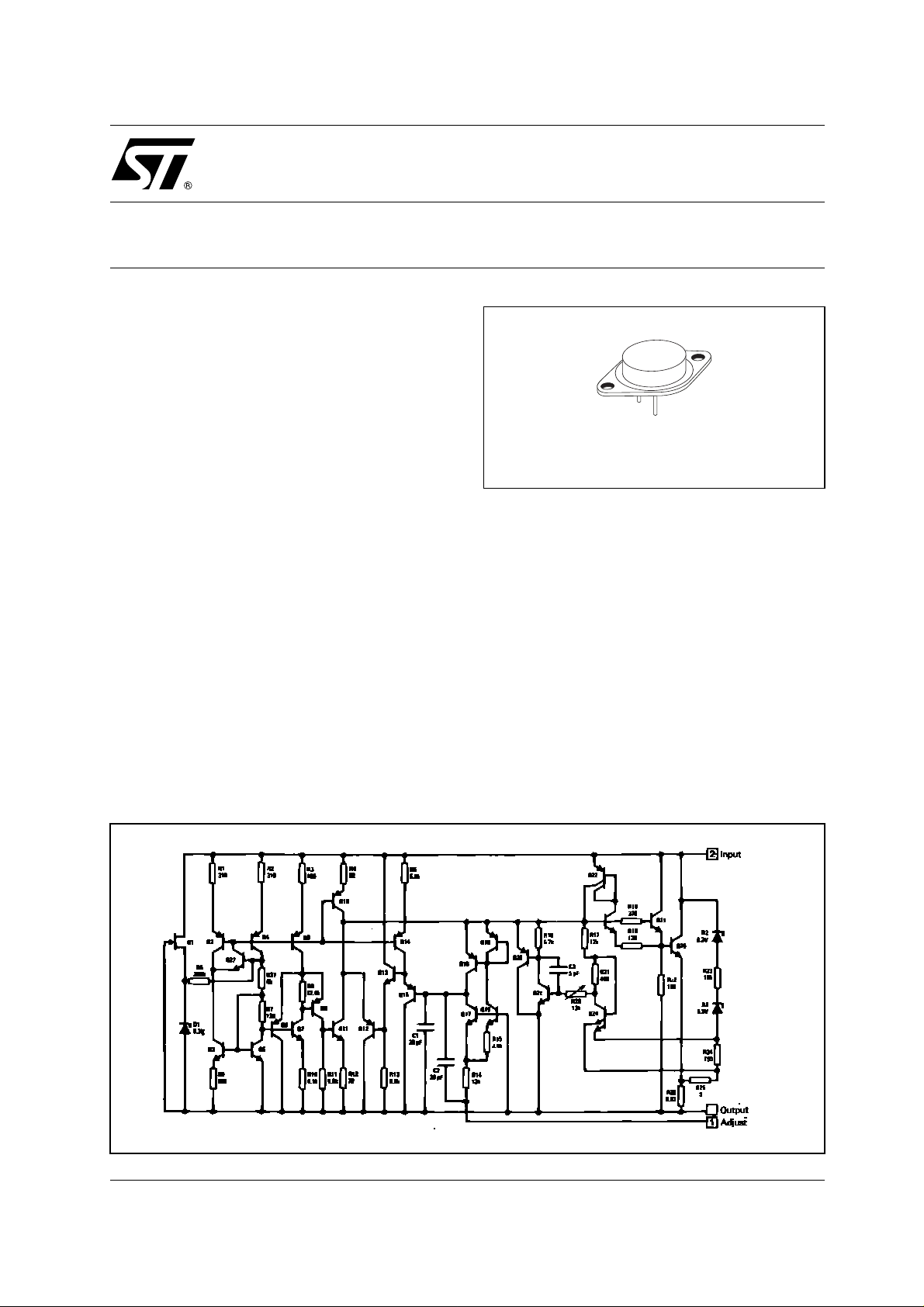
SCHEMATIC DIAGRAM
1/14April 2003
Page 2
LM138-LM238-LM338
difficult to achiev e with standard 3-terminal
regulators.
Besides replacing fixed regulators or disc rete
designs, the LM238 is useful in a wide variety of
other applications. Since the regulator i s "floating"
and sees only the input-to-outpu t differential
voltage, supplies of several hundred volts can be
regulated as long as the maximum input to input
differential is not exceeded.
The LM138/LM238/LM338 are packaged in
standard ste el TO-3 transistor packages. The
LM138 is rated for operation from -55°C to 150°C,
the LM 238 from –25°C to 150°C and the LM338
from 0°C to 125°C.
ABSOLUTE MAXIMUM RATINGS
Symbol Parameter Value Unit
V
I-VO
P
T
T
lead
T
oper
Absolute Maximum Ratings are those values beyond which damage to the device may occur. Functional operation under these condition is
not implied.
Input Output Voltage Differential
Power Dissipation
tot
Storage Temperature Range
stg
Lead Temperature (Soldering, 10 seconds)
Operating Junction Temperature Range LM138 -55 to 150
LM338 0 to 125
35 V
Internally Limited
-65 to 150 °C
300 °C
°CLM238 -25 to 125
THERMAL DATA
Symbol Parameter Value Unit
R
thj-case
R
thj-amb
Thermal Resistance Junction-case
Thermal Resistance Junction-ambient
1.4 °C/W
35 °C/W
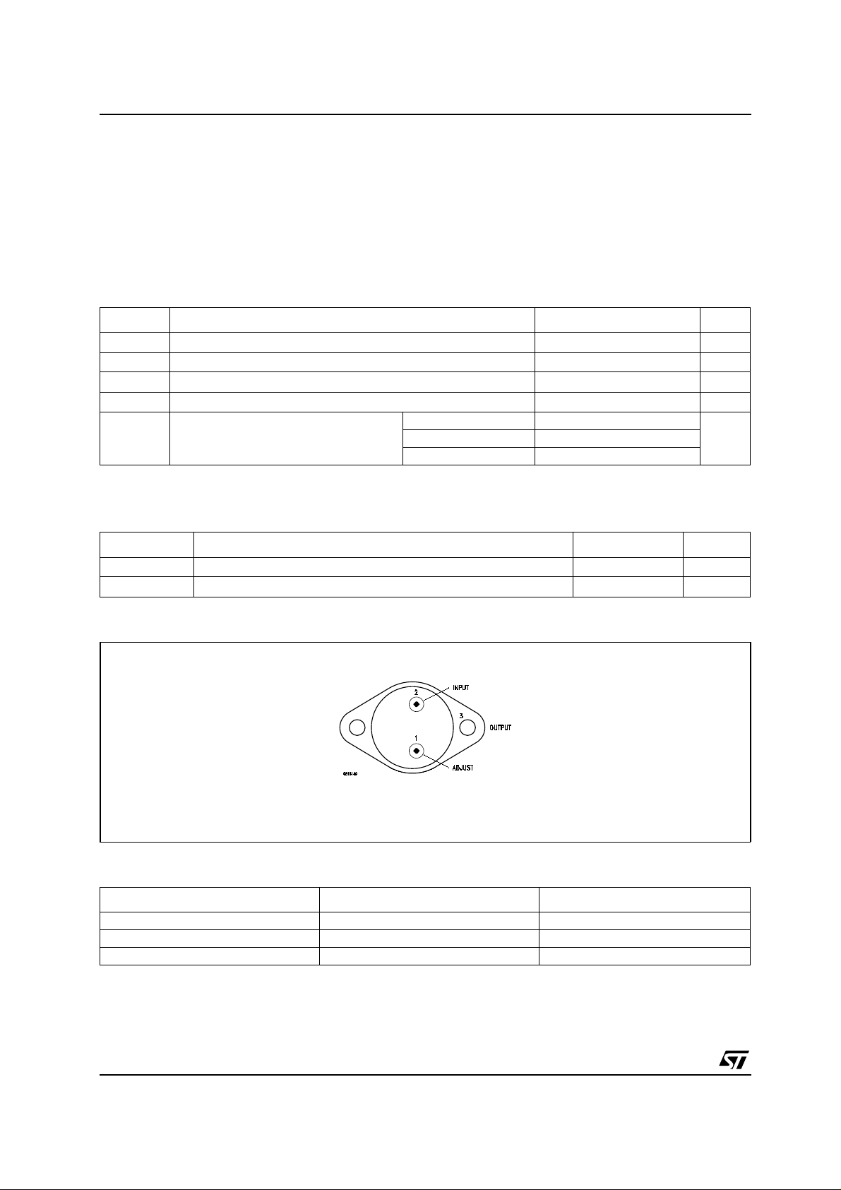
CONNECTION DIAGRAM (top view)
ORDERING CODES
TYPE TO-3 TEMPERATURE RANGE
LM138 LM138K -55°C to 150°C
LM238 LM238K -25°C to 150°C
LM338 LM338K 0°C to 125°C
TO-3
2/14
Page 3
LM138-LM238-LM338
ELECTRICAL CHARACTERISTICS OF LM138/LM238 (TJ= -55 to 150° C for LM138,
T
= -25 to 150°C for LM238, VI-VO=5V,IO= 2.5 A . Although power dissipation is internally limited, these
J
specifications apply to power dissipat ion up to 50W, unless otherwise specified).
Symbol Parameter Test Conditions Min. Typ. Max. Unit
Line Regulation (Note 1) Ta= 25°C, VI-VO= 3 to 35 V 0.005 0.01 %/V
K
VI
Load Regulation (Note 1) Ta= 25°C
K
VO
I
=10mAto5A
O
Thermal Regulation Pulse = 20 ms 0.002 0.01 %/W
I
Adjustment Pin Current 45 100 µA
adj
∆I
Adjustment Pin Current
adj
Change
Reference Voltage VI-VO= 3 to 35 V, IO=10mAto5A
V
ref
IL=10mAto5A VI-VO= 3 to 35 V 0.2 5 µA
P≤50 W
Line Regulation (Note 1) VI-VO= 3 to 35 V 0.02 0.04 %/V
K
VI
Load Regulation (Note 1) IO=10mAto5A VO≤5 V 20 30 mV
K
VO
K
Temperature Stability TJ=T
VT
I
O(min)
I
O(max)
V
Note 1: Regulation is measured at constant junction temperature. Changes in output voltage due to heating effects are taken into account
separately by thermal rejection.
Minimum Load Current VI-VO≤35 V 3.5 5 mA
Current Limit VI-VO≤10 V DC 5 8 A
RMS Output Noise
NO
(% of V
Ripple Rejection Ratio VO=10V,f=120Hz 60 dB
R
vf
Long Term Stability Ta= 125°C 0.3 1 %
K
VH
)
O
T
C
a
adj
to T
min
max
= 25°C f = 10 Hz to 10 KHz 0.003 %
=10µF 60 75
≤5V 5 15 mV
V
O
≥5 V 0.1 0.3 %
V
O
1.19 1.24 1.29 V
≥ 5 V 0.3 0.6 %
V
O
1%
0.5 ms Peak 7 12
V
=30V 1
I-VO
3/14
Page 4
LM138-LM238-LM338
ELECTRICAL CHARACTERISTICS OF LM338 (TJ= 0 to 150°C, VI-VO=5V,IO=2.5A.
Although power dissipation is internally limited, these specifications appl y to power dissipation up to 50W,
unless otherwise spec ified).
Symbol Parameter Test Conditions Min. Typ. Max. Unit
Line Regulation (Note 1) Ta= 25°C, VI-VO= 3 to 35 V 0.005 0.03 %/V
K
VI
Load Regulation (Note 1) Ta= 25°C
K
VO
I
=10mAto5A
O
Thermal Regulation Pulse = 20 ms 0.002 0.02 %/W
I
Adjustment Pin Current 45 100 µA
adj
∆I
Adjustment Pin Current
adj
Change
Reference Voltage VI-VO= 3 to 35 V, IO=10mAto5A
V
ref
IL=10mAto5A VI-VO= 3 to 35 V 0.2 5 µA
P≤50 W
Line Regulation (Note 1) VI-VO= 3 to 35 V 0.02 0.06 %/V
K
VI
Load Regulation (Note 1) IO=10mAto5A VO≤5 V 20 50 mV
K
VO
K
Temperature Stability TJ=T
VT
I
O(min)
I
O(max)
V
Note 1: Regulation is measured at constant junction temperature. Changes in output voltage due to heating effects are taken into account
separately by thermal rejection.
Minimum Load Current VI-VO≤35 V 3.5 10 mA
Current Limit VI-VO≤10 V DC 5 8 A
RMS Output Noise
NO
(% of V
Ripple Rejection Ratio VO=10V,f=120Hz 60 dB
R
vf
Long Term Stability Ta= 125°C 0.3 1 %
K
VH
)
O
T
C
a
adj
to T
min
max
= 25°C f = 10 Hz to 10 KHz 0.003 %
=10µF 60 75
≤5V 5 25 mV
V
O
≥5 V 0.1 0.5 %
V
O
1.19 1.24 1.29 V
≥ 5 V 0.3 1 %
V
O
1%
0.5 ms Peak 7 12
V
=30V 1
I-VO
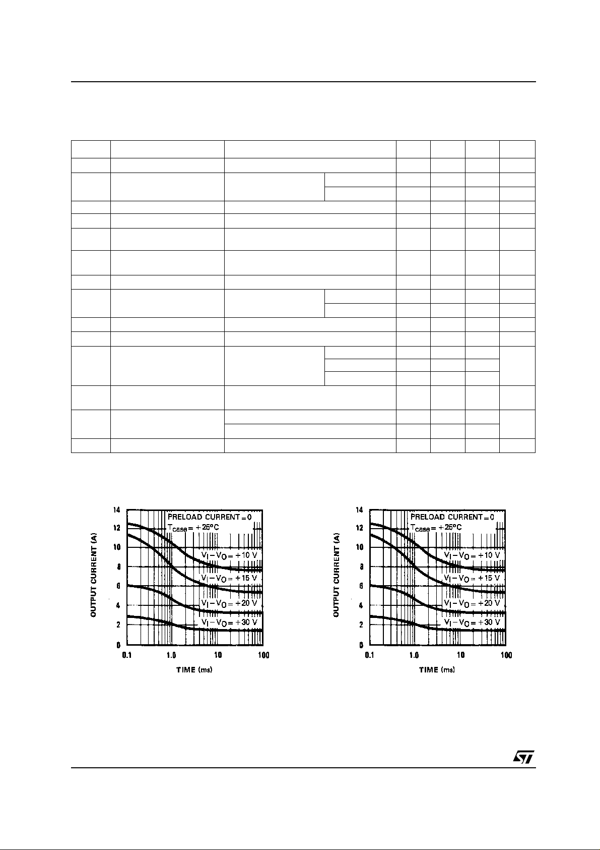
Figure1 : Current Limit Figure2 : Current Limit
4/14
Page 5
LM138-LM238-LM338
Figure3 : Current Limit
Figure4 : Load Regulation
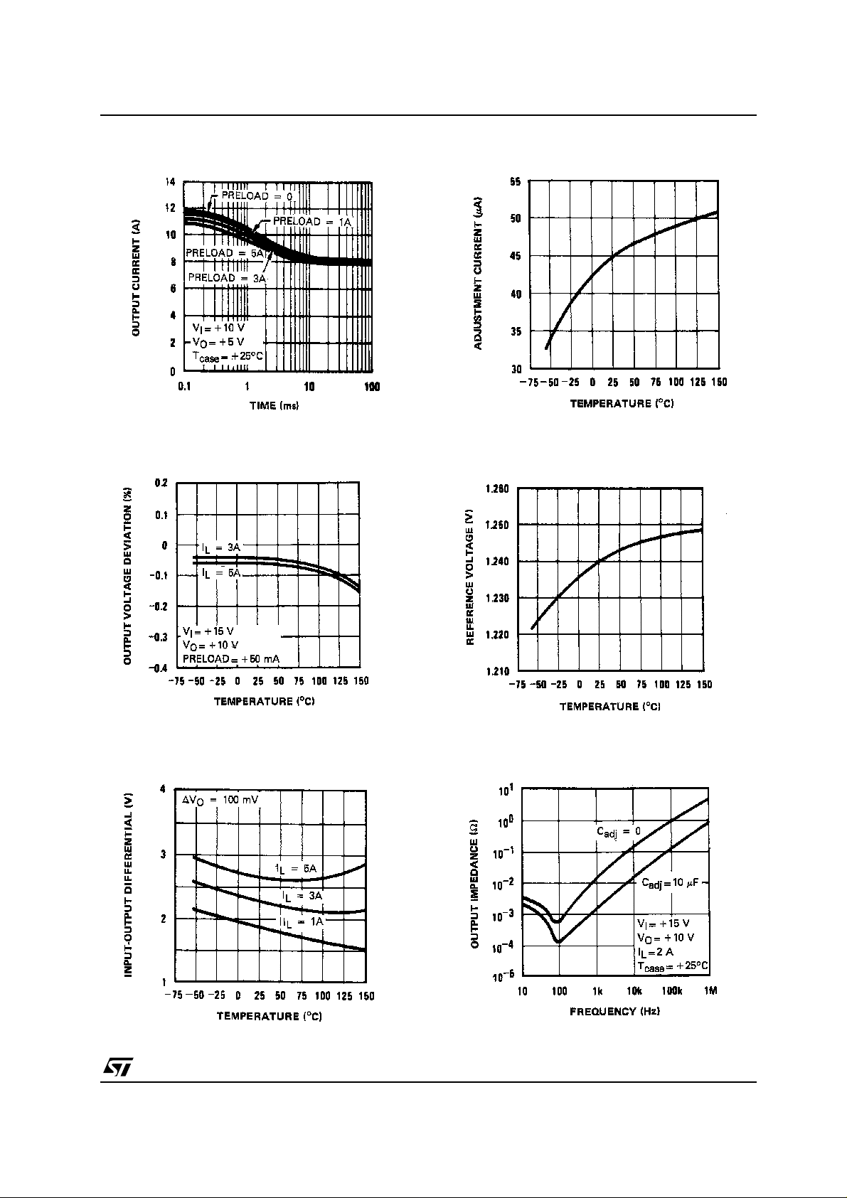
Figure6 : A djustment Current
Figure7 : Temperature Stability
Figure5 : Dropout Voltage
Figure8 : Output Impedance
5/14
Page 6

LM138-LM238-LM338
Figure9 : Minimum OperatingCurrent
Figure10 : Ripple Rej ec tion
Figure12 : Ripple Rej ec tion
Figure13 : Line Transient Response
Figure11 : Ripple Rej ec tion
6/14
Figure14 : Load Transient Response
Page 7

LM138-LM238-LM338
TYPICAL APPLICATIONS
1.2V to 25V ADJUSTABLE REGULATOR
Needed if device is far from filter capacitors.
* Optional-improves transient response. Output capacitors in the range of 1mF to 100mF of aluminium or tantalum electrolytic are commonly
used to provide improved output impedance and rejection of transients
** V
=1.25V(1+R2/R1)
O
*** R
= 240Ω for LM138 and LM238
1
APPLICATION HINTS
In operation, the LM338 develops a nominal 1.25V reference voltage, V
, between the output and
(ref)
adjustment terminal . The reference voltage is impressed across program resistor R
voltage is constant, a c onstant current I
then f lows throu gh the output set resistor R2, giving an output
1
voltage of
V
O=V(ref)
(1+ R2/R1)+I
adjR2
Figure15 :
and, since the
1
Since the 50µA c urrent from the adjustment terminal represents an error term, the LM338 was designed
to minimize I
and make it very constant with line and load c hanges. To do this, all quiescent operating
adj
current is returned to the output establishing a minimum load current requirement. If there is insufficient
load on the output, the output will rise.
7/14
Page 8

LM138-LM238-LM338
EXTERNAL CAPACITORS
An input bypass capacitor is recomm ended. A 0.1µF disc or 1µF solid tantalum on the input is suitable
input by passing for almost all applicati ons . The device is more sensitive to the absence of input
bypassing when adjustment or output capacitors are used by the above values will eliminate the
possibility of problems. The adjustment terminal can be bypassed to ground on the LM338 to improve
ripple rejection. This bypass capacitor prevents ripple form being amplified as the output voltage is
increased. With a 10µF by pas s capacitor 75dB ripple rejection is obtainable at any output level. Increases
over 20µF do not appreciably improve the ripple rejection at frequencies above 120Hz. If the bypass
capacitor is used, it is sometimes neces s ary to include protection diodes to prevent the capacitor from
discharging through internal low current paths and damaging the device. In general, the best type of
capacitors to use are solid tantalum. Solid tantalum capacitors have low i mpedance even at hi gh
frequencies. Depending upon capacitor construction, it takes about 25µF in aluminum electrolytic to equal
1µF solid tantalum at high frequencies. Ceramic capacitors are also good at hi gh frequencies, but som e
types have a large decrease in capacitance at frequencies around 0.5M Hz . For this reason, 0.01µF disc
may seem to work better t han a 0.1µF disc as a bypass. Although the LM338 is stable with no output
capacitors, like any feedback circuit, certain val ues of external capacitance c an cause excessive r inging.
This occurs wi th values between 500pF and 5000pF. A 1mF solid tantalum (or 25µF aluminium
electrolytic) on the output swamps this effect and i nsures stability.
LOAD REGULATION
The LM338 is capable of providing extremely good load regulation but a few precautions are needed to
obtain maximum performance. The current s et resistor connected between the adjustment terminal and
the output terminal (usually 240Ω)should be tied directly to the output of the regulator rather t han near the
load. This eliminates line drops from appearing effectively in series with the refere nce and degrading
regulation. For example, a 15V regulator with 0.05Ω resistance between the regulator and load will have
a load regulation due to line resistance of 0.05Ω x IL. If the s et resistor is connected near the load t he
effectivelineresistancewillbe0.05Ω(1 + R
effect of resistance between t he regulator and 140Ω set resistor. With the TO -3 package, it is easy to
minimize the resistance from the case to the set resistor, by using 2 s eparate leads to the case. T he
ground of R
can be returned near the ground of the lo ad t o prov ide remote ground sensing and improve
2
load regulation.
PROTECTION DIODES
When external capacitors are used with any IC regulator it is sometimes necessary to add prot ec tion
diodes to prevent the capacitors from dischargin g through low c urrent points into the regulator. Most 20µF
capacitors hav e low enough internal series resistance to deliver 20A spi ke s when shorted. Although the
surge is short, th ere is enough energy to d amage parts of the IC. W hen an output capacit or is connected
to a regulator and the input is shorted, the out put capacitor will discharge into the output of the regulator.
The discharge current depends o n the value of the capacitor, the ou tput voltage of the regulator, and the
rate of dec reas e of V
. In the LM338 this discharge path is through a large junction that is able to sustain
I
25A surge with no probl em. This is not true of other types of positive regulators. For output capacitors of
100µF or less at output of 15V or less, there is no need to use diodes.The bypass capacitor on the
adjustment terminal can discharge through a low c urrent junction . Discharge occurs when either the input
or output is shorted. Internal to the LM338 is a 50Ω resis tor which limits the peak discharge current. N o
protection is n eeded for output vol tages of 25V or less and 10µF capacitance. Figure 3 shows an LM338
with protection diodes included for use with outputs greater than 25V and high values of output
capacitance output c apac itanc e an LM338 with protec tion diodes included for use with outputs greater
than 25V and high values of output capacitance
) or in this c as e, 11.5 times worse. Figure 2 shows t he
2/R1
8/14
Page 9

Figure16 : REGULATOR W ITH LINE R ESISTANCE IN OUTPUT LEAD
Figure17 : REGULATOR W ITH PRO TECTION DIODES
LM138-LM238-LM338
9/14
Page 10

LM138-LM238-LM338
Figure18 : 10 A REGULATOR
* Minimum Load -100mA
VI≥ 10V
≥ 3V
V
O
VI-VO≥ 3.5V
Figure19 : 5A CURRENT REGULATOR
* Minimum Load -100mA
≥ 10V
V
I
VO≥ 3V
10/14
Page 11

Figure20 : 15A REGULATOR
LM138-LM238-LM338
* Minimum Load -100mA
V
≥ 10V
I
≥ 3V
V
O
V
≥ 4V
I-VO
Figure21 : 5V LOGIC REGULATOR WITH ELECTRONIC SHUTDOWN
*R1=240Ωfor LM138 or LM238
*R
=720Ω for LM138 or LM238
2
** Minimum Load -100mA
11/14
Page 12

LM138-LM238-LM338
Figure22 : TRACKING PREREGULATOR
*R1=240Ωfor LM138 or LM238
*R
=720Ω for LM138 or LM238
2
* * Minimum output= 1.2V
Figure23 : SLOW TURN-ON 15V REGULATOR
*R1=240Ωfor LM138 or LM238
=2.7kΩ for LM138 or LM238
*R
2
12/14
Page 13

TO-3 MECHANICAL DATA
LM138-LM238-LM338
DIM.
A 11.85 0.466
B 0.96 1.05 1.10 0.037 0.041 0.043
C 1.70 0.066
D 8.7 0.342
E 20.0 0.787
G 10.9 0.429
N 16.9 0.665
P 26.2 1.031
R 3.88 4.09 0.152 0.161
U 39.5 1.555
V 30.10 1.185
MIN. TYP MAX. MIN. TYP. MAX.
mm. inch
P
A
G
U
V
N
O
B
D
C
E
R
P003C/C
13/14
Page 14

LM138-LM238-LM338
Information furnished is believed to be accurate and reliable. However, STMicroelectronics assumes no responsibility for the
consequences of use o f suc h inf ormat ion n or f or an y infr ingeme nt of paten ts or oth er ri gh ts of third part ies whic h may resul t f rom
its use. No license is granted by implication or otherwise under any patent or patent rights of STMicroelectronics. Specifications
mentioned in this publication are subject to change without notice. This publication supersedes and replaces all information
previously supplied. STMicroelectronics products are not authorized for use as critical components in life support devices or
systems without express written approval of STMicroelectronics.
Australia - Brazil - Canada - China - Finland - France - Germany - Hong Kong - India - Israel - Italy - Japan - Malaysia - Malta - Morocco
© The ST logo is a registered trademark of STMicroelectronics
© 2003 STMicroelectronics - Printed in Italy - All Rights Reserved
STMicroelectronics GROUP OF COMPANIES
Singapore - Spain - Sweden - Switzerland - United Kingdom - United States.
© http://www.st.com
14/14
 Loading...