

Page 1

LM123/LM223
LM323
THRE E-TERMINA L 3A-5V
POSITIVE VOLTAG E REGULATORS
■ OUTPUT CURRENT : 3A
■ INTERNAL CURRENT AND THERMAL
LIMITING
■ TYPICAL OUTPUT IMPEDANCE: 0.01Ω
■ MINIMUM INPUT VOLTAGE: 7.5V
■ POWER DISSIPATION: 30W
DESCRIPTION
The LM123, LM223, LM323 are three-terminal
positive voltage regulators with a preset 5V output
and a load driving capability of 3A. New circuit
design and processing techniques are used to
provide the high o utput curren t without sac rificing
the regulation characteristics of lower current
devices.
The 3A regulator is virtually blowout proof.
Current limiting, power limiting and thermal
shut-down provide the same high level of reliability
obtained with these techniqu es in the LM209, 1A
regulator. An overall worst case specification for
the combined effects of input voltage, load
current, ambient temperature, and power
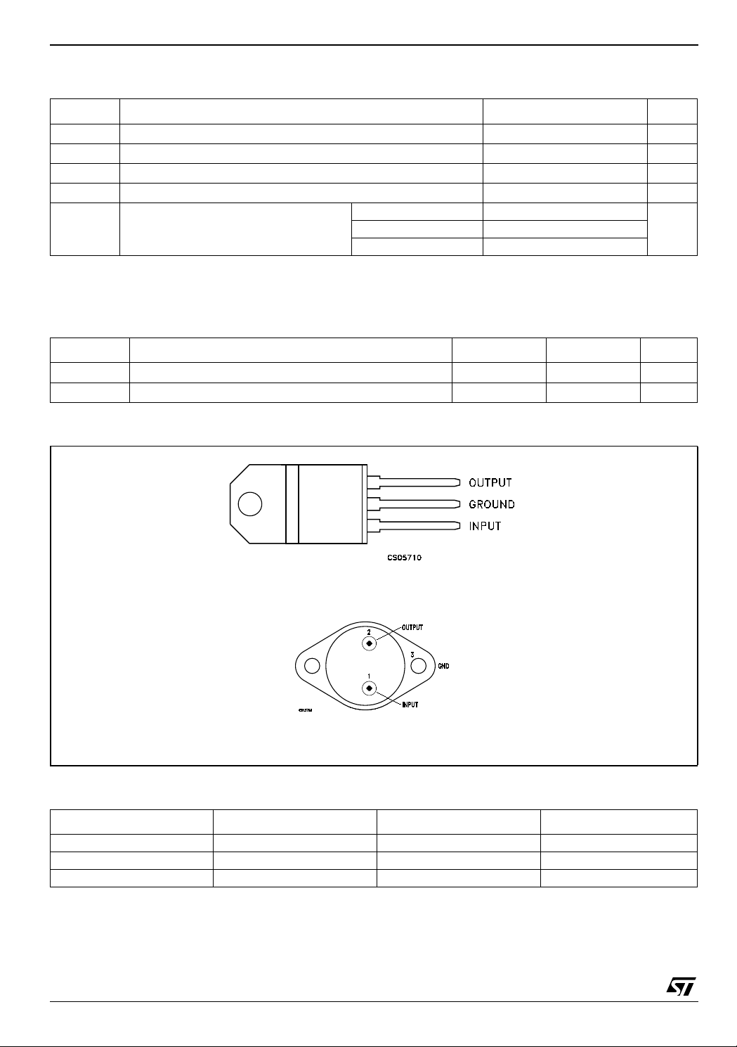
TO-220
TO-3
dissipation ensure that the LM123, LM223, LM323
will perform satisfactorily as a system element.
SCHEMATIC DIAGRAM
Rev. 3
1/11November 2005
Page 2
LM123-LM223-LM323
Table 1: Absolute Maximum Ratings
Symbol Parameter Value Unit
V
I
P
T
T
oper
Absolute Maximum Ratings are those values beyond which damage to the device may occur. Functional operation under these condition is
not implied.
Table 2: Thermal Data
Symbol Parameter TO-220 TO-3 Unit
R
thj-case
R
thj-amb
Figure 1: Conn ection Di agram (top view)
Input Voltage
I
Output Current
O
Power Dissipation
tot
Storage Temperature Range
stg
Operating Junction Temperature Range LM123 -55 to 150
LM323 0 to 125
Thermal Resistance Junction-case Max
Thermal Resistance Junction-ambient Max
32°C/W
50 35 °C/W
20 V
Internally Limited
Internally Limited
-65 to 150 °C
°CLM223 -25 to 125
Table 3: Order Codes
TYPE TO-220 TO-3 TEMPERATURE RANGE
LM123 LM123K -55°C to 150°C
LM223 LM223K -25°C to 150°C
LM323 LM323T LM323K 0°C to 125°C
2/11
TO-220
TO-3
Page 3

LM123-LM223-LM323
Table 4: Electrical Characteristics Of LM123/LM223 (TJ = -55 to 150°C for LM123,
= -25 to 150°C for LM223 unless otherwise specified).
T
J
Symbol Parameter Test Conditions Min. Typ. Max. Unit
V
Output Voltage Range
O
(Note 2)
V
Output Voltage Range
O
(Note 2)
K
Line Regulation (Note 3) VI = 7.5 to 15 V TJ = 25°C 5 25 mV
VI
Load Regulation (Note 3) IO = 0 to 3 AVI = 7.5 V TJ = 25°C 25 100 mV
K
VO
Quiescent Current VI = 7.5 to 15 V IO = 0 to 3 A 12 20 mA
I
IB
Output Noise Voltage Ta = 25°C f = 10 Hz to 100 KHz 40 µV
V
NO
I
Short Circuit Current Limit VI = 15 V TJ = 25°C 3 4.5 A
OS
Long Term Stability 35 mV
K
VH
Notes: 1. Although power dissipation is internally limited, specifications apply only for P ≤ 30W.
2. Select ed devices with tighten ed t ol erance out put voltage avai l able.
3. Load and line regulation are specif i ed at constant j unction temperature. Pulse testi ng is require d wi t h a pulse width ≤ 1m s and
duty cycle ≤ 5%.
Table 5: Electrical Characteristics Of LM323 (TJ = 0 to 150°C, unless otherwise specified).
Ta = 25°C, VI = 7.5 V, IO = 0 4.7 5 5.3 V
TJ = T
min
to T
max
P ≤ P
max
4.6 5.4 V
VI = 7.5 to 15 V IO = 0 to 3 A
= 7.5 V TJ = 25°C 4 5
V
I
rms
Symbol Parameter Test Conditions Min. Typ. Max. Unit
V
Output Voltage Range
O
(Note 2)
V
Output Voltage Range
O
(Note 2)
Line Regulation (Note 3) VI = 7.5 to 15 V TJ = 25°C 5 25 mV
K
VI
K
Load Regulation (Note 3) IO = 0 to 3 AVI = 7.5 V TJ = 25°C 25 100 mV
VO
Quiescent Current VI = 7.5 to 15 V IO = 0 to 3 A 12 20 mA
I
IB
Output Noise Voltage Ta = 25°C f = 10 Hz to 100 KHz 40 µV
V
NO
I
Short Circuit Current Limit VI = 15 V TJ = 25°C 3 4.5 A
OS
Long Term Stability 35 mV
K
VH
Notes: 1. Although power dissipation is internally limited, specifications apply only for P ≤ 30W.
2. Select ed devices with tighten ed t ol erance out put voltage avai l able.
3. Load and line regulation are specif i ed at constant j unction temperature. Pulse testi ng is require d wi t h a pulse width ≤ 1m s and
duty cycle ≤ 5%.
Ta = 25°C, VI = 7.5 V, IO = 0 4.8 5 5.2 V
TJ = T
min
to T
max
P ≤ P
max
4.75 5.25 V
VI = 7.5 to 15 V IO = 0 to 3 A
V
= 7.5 V TJ = 25°C 4 5
I
rms
3/11
Page 4
LM123-LM223-LM323
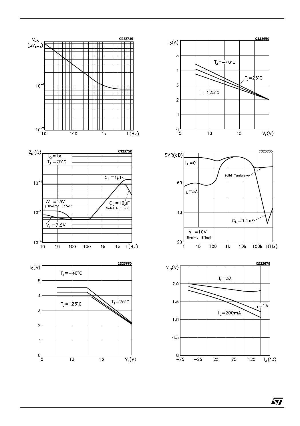
Figure 2: Output Noise Voltage
Figure 3: Output Impedance
Figure 5: Short Circuit Current
Figure 6: Ripple Rejection
Figure 4: Peak Available Output Current
4/11
Figure 7: Dropout Voltage
Page 5

LM123-LM223-LM323
Figure 8: Line Transient Response
Figure 9: Output Voltage
Figure 10: Quiescent Current
Figure 11: Load Transient Response
5/11
Page 6

LM123-LM223-LM323
TYPICAL APPLICATION
Figure 12: Basic 3A Regulator
C1 = Required if regulator is distant from filter capacitors.
CL = Regulator is st able with no lo ad capacitor into resistiv e l oads.
Figure 13: Trimming Output To 5V
6/11
Page 7

Figure 14: 10A Regulator With Complete Overload Protection
LM123-LM223-LM323
* Selected for 20 mA cu rrent from unr egulated negative supply.
** Solid tantalum.
A = LM101A, LM 201A, LM301A.
Figure 15: Adjustable Regulator 0 - 10V/3A
A1 = LM101A, LM201A, LM301A.
CI = 2µF optional - improves ripple rejection, noise and transient response.
7/11
Page 8
LM123-LM223-LM323
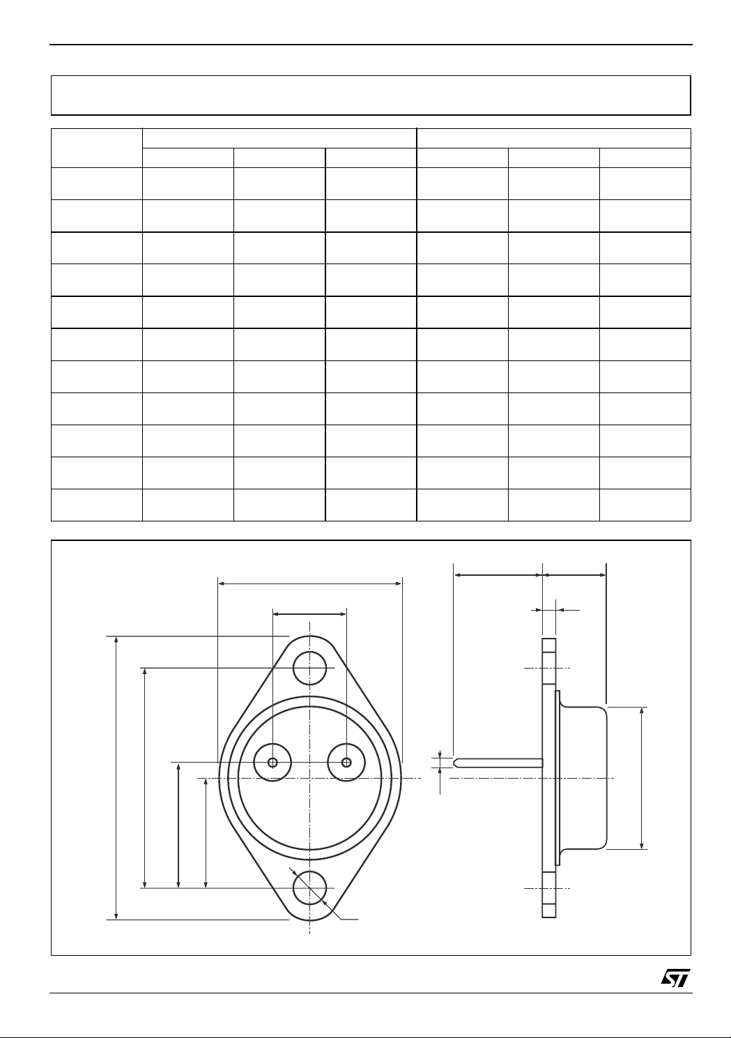
TO-3 MECHANICAL DATA
DIM.
A 11.85 0.466
B 0.96 1.05 1.10 0.037 0.041 0.043
C 1.70 0.066
D 8.7 0.342
E 20.0 0.787
G 10.9 0.429
N 16.9 0.665
P 26.2 1.031
R 3.88 4.09 0.152 0.161
U 39.5 1.555
V 30.10 1.185
MIN. TYP MAX. MIN. TYP. MAX.
mm. inch
P
A
G
U
V
N
O
B
D
C
E
R
P003C/C
8/11
Page 9

LM123-LM223-LM323
TO-220 MECHANICAL DAT
DIM.
A 4.40 4.60 0.173 0.181
C 1.23 1.32 0.048 0.051
D 2.40 2.72 0.094 0.107
D1 1.27 0.050
E 0.49 0.70 0.019 0.027
F 0.61 0.88 0.024 0.034
F1 1.14 1.70 0.044 0.067
F2 1.14 1.70 0.044 0.067
G 4.95 5.15 0.194 0.203
G1 2.4 2.7 0.094 0.106
H2 10.0 10.40 0.393 0.409
L2 16.4 0.645
L4 13.0 14.0 0.511 0.551
L5 2.65 2.95 0.104 0.116
L6 15.25 15.75 0.600 0.620
L7 6.2 6.6 0.244 0.260
L9 3.5 3.93 0.137 0.154
DIA. 3.75 3.85 0.147 0.151
MIN. TYP MAX. MIN. TYP. MAX.
mm. inch
A
P011C
9/11
Page 10

LM123-LM223-LM323
Table 6: Revision History
Date Revision Description of Change s
04-Nov-2005 3 Updated curves, no content change.
10/11
Page 11

LM123-LM223-LM323
Information furnished is believed to be accurate and reliable. However, STMicroelectronics assumes no responsibility for the consequences
of use of such information nor for any infringement of patents or other rights of third parties which may result from its use. No license is granted
by implic ati o n or ot h er wis e und er an y pat ent or pa te nt r igh ts of STMi cr oe l ect ro ni cs . Sp ec if i cat i on s ment i o ned i n th is p ub li c ati on ar e s ubj ec t
to change without notice. This publication supersedes and replaces all information previously suppl ied. STMicroelectronics products are not
authorized for use as critical components in life support devices or systems without express written approval of STMicroelectronics.
The ST logo is a registered trademark of STMicroelectronics
All other names are the property of their respective owners
© 2005 STMicroelectronics - All Rights Reserved
STMicroelectronics group of companies
Australia - Belgium - Brazil - Canada - China - Czech Republic - Finland - France - Germany - Hong Kong - India - Israel - Italy - Japan -
Malaysia - Malta - Morocco - Singapore - Spain - Sweden - Switzerland - United Kingdom - United States of America
www.st.com
11/11
 Loading...