

Page 1

LM111
LM211 - LM311
VOLTAGE COMPARATORS
■ MAXIMUM INPUT CURRENT : 150nA
■ MAXIMUM OFFSET CURRENT : 20nA
■ DIFFERENTIAL INPUT VOLTAGE RANGE :
±30V
■ POWER CONSUMPTION :135mW AT ±15V
■ SUPPLY VOLTAGE : +5V TO ± 1 5 V
■ OUTPUT CURRENT : 50mA
DESCRIPTION
The LM111, LM211, LM311 are voltage comparators that have low input currents.
They are also designed to operate over a wide
range of supply voltages : from standard ±15V operational amplifier supplies down to the single +5V
supply used for IC logic.
Their output is compatible with RTL-DTL and TTL
as well as MOS c ircuits and can switch voltages
up to +50V at outputs currents as high as 50mA.
N
DIP8
D
SO8
PIN CONNECTIONS (top view)
1
8
ORDER CODE
Part Number
LM111 -55°C, +125°C
LM211 -40°C, +105°C
LM311 0°C, +70°C
Example : LM311D
N = Dual in Line Package (DIP)
D = Small Outline Package (SO) - also available in Tape & Reel (DT)
June 2002
Temperature
Range
Package
ND
••
••
••
2
3
4
1 - Ground
2 - Non-inverting input
3 - Inverting input
-
4 - V
CC
7
6
5
5 - Balance
6 - Strobe/Balance
7 - Output
8 - V
CC
+
1/9
Page 2

LM111-LM211-LM311
SCHEMATIC DIAGRAM
ABSOLUTE MAXIMUM RATINGS
Symbol Parameter Value Unit
V
V
V
Supply Voltage 36 V
CC
V
Differential Input Voltage ±30 V
id
V
Input Voltage
i
Ground to Negative Supply Voltage 30 V
(1-4)
Output to Negative Supply Voltage LM111-LM211
(7-4)
1)
±15 V
50
LM311
40
V
Output Short-Circuit Duration 10 s
Voltage at strobe pin
Power Dissipation 2) DIP8
p
d
T
Junction Temperature +150 °C
j
T
1. This rating applies for ±15V supplies. The positive input voltage limit is 30V above the negative. The negative input voltage is equal to the
negative supply voltage or 30V below the positive supply, whichever is less.
2. Pd is calculated with T
Storage Temperature Range -65 to +150 °C
stg
= +25°C, Tj = +150°C and R
amb
SO8
= 100°C/W for DIP8 package
thja
= 175°C/W for SO8 package
V
CC
1250
710
+
-5
V
mW
OPERATING CONDITIONS
Symbol Parameter Value Unit
V
T
Supply Voltage 5 to ±15 V
CC
Operating Free-Air Temperature range LM111
oper
LM211
LM311
-55 to +125
-40 to +105
0 to +70
°C
2/9
Page 3
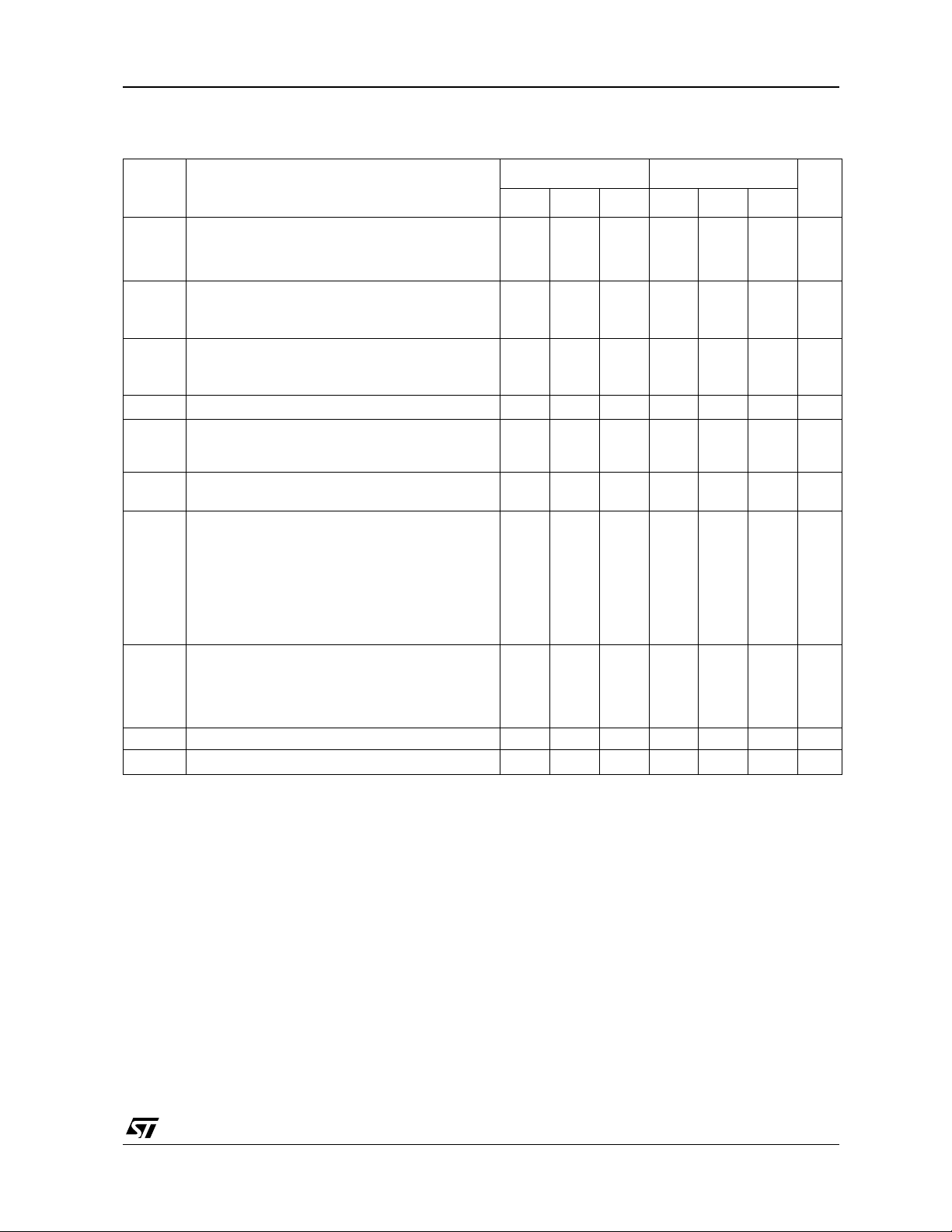
ELECTRICAL CHARACTERISTICS
+
V
= ±15V, T
CC
Symbol Parameter
= +25°C (unless otherwise specified)
amb
LM111-LM211-LM311
LM111 - LM211 LM311
Unit
Min. Typ. Max. Min. Typ. Max.
Input Offset Voltage (RS ≤ 50kΩ)- note 1)
V
io
T
T
amb
min
= +25°C
≤ T
amb
≤ T
max
0.7 3
27.5
4
10
Input Offset Current -(see note 1)
T
T
amb
min
= +25°C
≤ T
amb
≤ T
max
410
20
650
70
I
io
Input Bias Current - (see note 1 )
T
I
ib
A
Large Signal Voltage Gain 40 200 40 200 V/mV
vd
+
I
I
V
Supply Currents
CC
-
CC
Input Common Mode Voltage Range
icm
= +25°C
amb
T
≤ T
min
Positive
Negative
≤ T
T
min
amb
amb
≤ T
≤ T
max
max
60 100
5.1
4.1
-14.5 +13.8
-14.7
100 250
150
6
5
5.1
4.1
+13 -14.5 +13.8
-14.7
300
7.5
5
+13 V
Low Level Output Voltage
= +25°C, IO = 50mA Vi ≤ -5mV
T
amb
T
≤ T
V
OL
min
V
CC
I
= 8mA Vi ≤ -6m
O
≤ T
amb
+
≥ +4.5V, V
max
CC
-
= 0
V
≤ -10mV
i
V
≤ -10mV
i
0.75
0.23
1.5
0.4
0.75
0.23
1.5
0.4
High Level Output Current
I
OH
T
amb
Vi ≥ +10mV,Vo = +5V
≤ T
≤ T
T
min
amb
Vi ≥ +5mV,Vo = +35V
max
0.2
0.2 50nAnA
0.1100.5
= +25°C Vi ≥ +5mV,Vo = +35V
Istrobe Strobe Current 3 3 mA
t
Response Time - note
re
1. The offset voltage, offset current and bias current specifications apply for any supply voltage from a single +5V suplly up to ±15V
supplies
The offset voltages and offset currents given are the maximum values required to drive the output down to +1V or up to +14V with a
1mA load current. Thus, these parameters define an error band and take into account the worst-case of voltage gain and input im
pedance.
2. The response time specified (see definitions) is for a 100mV input step with 5mV overdrive.
2)
200 200 ns
mV
nA
nA
mA
V
µ
A
3/9
Page 4

LM111-LM211-LM311
4/9
Page 5

LM111-LM211-LM311
5/9
Page 6

LM111-LM211-LM311
6/9
Page 7

LM111-LM211-LM311
7/9
Page 8

LM111-LM211-LM311
PACKAGE MECHANICAL DATA
8 PINS - PLASTIC DIP
Dimensions
Min. Typ. Max. Min. Typ. Max.
A 3.32 0.131
a1 0.51 0.020
B 1.15 1.65 0.045 0.065
b 0.356 0.55 0.014 0.022
b1 0.204 0.304 0.008 0.012
D 10.92 0.430
E 7.95 9.75 0.313 0.384
e 2.54 0.100
e3 7.62 0.300
e4 7.62 0.300
F 6.6 0260
i 5.08 0.200
L 3.18 3.81 0.125 0.150
Z 1.52 0.060
Millimeters Inches
8/9
Page 9

PACKAGE MECHANICAL DATA
8 PINS - PLASTIC MICROPACKAGE (SO)
a2
LM111-LM211-LM311
L
c1
C
A
a3
b
e3
D
8
1
M
5
4
s
F
a1
E
b1
Millimeters Inches
Dimensions
Min. Typ. Max. Min. Typ. Max.
A 1.75 0.069
a1 0.1 0.25 0.004 0.010
a2 1.65 0.065
a3 0.65 0.85 0.026 0.033
b 0.35 0.48 0.014 0.019
b1 0.19 0.25 0.007 0.010
C 0.25 0.5 0.010 0.020
c1 45° (typ.)
D 4.8 5.0 0.189 0.197
E 5.8 6.2 0.228 0.244
e 1.27 0.050
e3 3.81 0.150
F 3.8 4.0 0.150 0.157
L 0.4 1.27 0.016 0.050
M 0.6 0.024
S 8° (max.)
Information furnished is bel ieved to be accurate and reliable. However, STMicroe lectronics assumes no responsibility for the
consequences of use of such information nor for any infringement of patents or other rights of third parties which may result from
its use. No li cense is granted by i mp lication or otherwise under any patent or patent rights of STMicroelec tron ic s. S pec ificat ions
mentioned in this publication ar e subject to change without notice. This publication supersedes and replaces all information
previously supplied. S TMicroelectronics products are not authorized for use as critica l components in life suppo rt devices or
systems without express written approval of STMicroelectronics.
© The ST logo is a registered trademark of STMicroelectronics
© 2002 STM icroelectronics - P r i n ted in Italy - All Rights Reserved
STMicr o el ectronics GROUP OF COMPA NI ES
Australi a - Brazil - Canada - Chin a - F i nl and - France - Germany - Hong Kong - India - Israel - Italy - Japa n - Malaysia
Malta - Mor occo - Singapore - Spain - Sweden - S wi t zerland - U ni ted Kingdom - United Sta tes
© http://www.st.com
9/9
 Loading...