


www.DataSheet4U.com
2-axis - +/-2g ULTRACOMPACT LINEAR ACCELEROMETER
Features
■ 2.4V TO 5.25V SINGLE SUPPLY
OPERATION
■ LOW POWER CONSUMPTION
■ ±2g FULL-SCALE
■ 0.3mg RESOLUTION OVER 100Hz
BANDWIDTH
■ EMBEDDED SELF TEST
■ OUTPUT VOLTAGE, OFFSET AND
SENSITIVITY RATIOMETRIC TO THE
SUPPLY VOLTAGE
■ HIGH SHOCK SURVIVABILITY
■ ECO-PACK COMPLIANT
Description
The LIS2L02AL is a low-power 2-axis linear
capacitive accelerometer that includes a sensing
element and an IC interface able to take the
information from the sensing element and to
provide an analog signal to the external world.
The sensing element, capable of detecting the
acceleration, is manufactured using a dedicated
process developed by ST to produce inertial
sensors and actuators in silicon.
The IC interface is manufactured using a standard
CMOS process that allows high level of integration
LIS2L02AL
MEMS INERTIAL SENSOR:
LGA-8
to design a dedicated circuit which is trimmed to
better match the sensing element characteristics.
The LIS2L02AL has a full scale of
capable of measuring accelerations over a
bandwidth of 2.0 kHz for all axes. The device
bandwidth may be reduced by using external
capacitances. A self-test capability allows to
check the mechanical and electrical signal path of
the sensor.
The LIS2L02AL is available in plastic SMD
package and it is guaranteed to operate over an
extended temperature range of -40°C to +85°C.
The LIS2L02AL belongs to a family of products
suitable for a variety of applications:
– Mobile terminals
– Gaming and Virtual Reality input devices
– Free-fall detection for data protection
– Antitheft systems and Inertial Navigation
– Appliance and Robotics.
±2g and it is
Order codes
Part number Temp range, °C Package Packing
LIS2L02AL -40°C to +85°C LGA-8 Tray
LIS2L02ALTR -40°C to +85°C LGA-8 Tape & Reel
Rev 1
September 2005 CD00068420 1/17
www.st.com
17

LIS2L02AL
Contents
1 Block Diagram & Pins Description . . . . . . . . . . . . . . . . . . . . . . . . . . . . . . . 3
1.1 Block diagram . . . . . . . . . . . . . . . . . . . . . . . . . . . . . . . . . . . . . . . . . . . . . . . . . 3
1.2 Pin Description . . . . . . . . . . . . . . . . . . . . . . . . . . . . . . . . . . . . . . . . . . . . . . . . 3
2 Mechanical and Electrical Specifications . . . . . . . . . . . . . . . . . . . . . . . . . . 5
2.1 Mechanical Characteristics . . . . . . . . . . . . . . . . . . . . . . . . . . . . . . . . . . . . . . . 5
2.2 Electrical Characteristics . . . . . . . . . . . . . . . . . . . . . . . . . . . . . . . . . . . . . . . . 6
2.3 Absolute maximum ratings . . . . . . . . . . . . . . . . . . . . . . . . . . . . . . . . . . . . . . . 7
2.4 Terminology . . . . . . . . . . . . . . . . . . . . . . . . . . . . . . . . . . . . . . . . . . . . . . . . . . . 7
3 Functionality . . . . . . . . . . . . . . . . . . . . . . . . . . . . . . . . . . . . . . . . . . . . . . . . . 9
3.1 Sensing element . . . . . . . . . . . . . . . . . . . . . . . . . . . . . . . . . . . . . . . . . . . . . . . 9
3.2 IC Interface . . . . . . . . . . . . . . . . . . . . . . . . . . . . . . . . . . . . . . . . . . . . . . . . . . . 9
3.3 Factory calibration . . . . . . . . . . . . . . . . . . . . . . . . . . . . . . . . . . . . . . . . . . . . . . 9
4 Application hints . . . . . . . . . . . . . . . . . . . . . . . . . . . . . . . . . . . . . . . . . . . . . 10
4.1 Soldering information . . . . . . . . . . . . . . . . . . . . . . . . . . . . . . . . . . . . . . . . . . 11
4.2 Output Response vs Orientation . . . . . . . . . . . . . . . . . . . . . . . . . . . . . . . . . . 11
5 Typical performance characteristics . . . . . . . . . . . . . . . . . . . . . . . . . . . . . 12
5.1 Mechanical Characteristics at 25°C . . . . . . . . . . . . . . . . . . . . . . . . . . . . . . . 12
5.2 Mechanical Characteristics derived from measurement in the
-40°C to +85°C temperature range . . . . . . . . . . . . . . . . . . . . . . . . . . . . . . . . 13
5.3 Electrical characteristics at 25°C . . . . . . . . . . . . . . . . . . . . . . . . . . . . . . . . . 14
6 Package Information . . . . . . . . . . . . . . . . . . . . . . . . . . . . . . . . . . . . . . . . . . 15
7 Revision history . . . . . . . . . . . . . . . . . . . . . . . . . . . . . . . . . . . . . . . . . . . . . . 16
2/17 CD00068420

LIS2L02AL 1 Block Diagram & Pins Description
1 Block Diagram & Pins Description
1.1 Block diagram
Figure 1. Block Diagram
X+
Y+
a
Y-
X-
SELF TEST
1.2 Pin Description
Figure 2. Pin Connection
MUX
REFERENCE
CHARGE
AMPLIFIER
TRIMMING CIRCUIT
DEMUX
S/H
S/H
CLOCK
Routx
Routy
Voutx
Vouty
X
1
Y
DIRECTION OF THE
DETECTABLE
ACCELERATIONS
LIS2L02AL
Vdd
Voutx
Vouty
Reserved
Reserved
BOTTOM VIEW
CD00068420 3/17
ST
NC
GND
1 Block Diagram & Pins Description LIS2L02AL
Table 1. Pin description
Pin # Pin Name Function
1 ST Self Test (Logic 0: normal mode; Logic 1: Self-test)
2 NC Not connected
3 GND 0V supply
4 Reserved Leave unconnected
5 Reserved Leave unconnected
6 Vouty Output Voltage Y channel
7 Voutx Output Voltage X channel
8 Vdd Power supply
4/17 CD00068420

LIS2L02AL 2 Mechanical and Electrical Specifications
2 Mechanical and Electrical Specifications
2.1 Mechanical Characteristics
Table 2. Mechanical Characteristics1
(Temperature range -40°C to +85°C) All the parameters are specified @ Vdd =3.3V,
T = 25°C unless otherwise noted.
Symbol Parameter Test Condition Min.
Typ.
2
Max. Unit
Ar
So
SoDr
Voff
OffDr
NL
CrossAx
An
Vt
Acceleration Range
Sensitivity
Sensitivity Change Vs
Temperature
Zero-g Level
Zero-g level Change Vs
Temperature
Non Linearity
Cross-Axis
Acceleration Noise
Density
Self test Output Voltage
Change
4
6
7,8
3
4
5
±1.8 ±2.0 g
Full-scale = 2g Vdd/5–10% Vdd/5 Vdd/5+10% V/g
Delta from +25°C ±0.01 %/°C
T = 25°C Vdd/2-6% Vdd/2 Vdd/2+6% V
Delta from +25°C ±0.2 mg/°C
Best fit straight line
Full-scale = 2g
X, Y axis
Vdd=3.3V;
Full-scale = 2g
T = 25°C
Vdd=3.3V
Full-scale = 2g
X axis
T = 25°C
Vdd=3.3V
Full-scale = 2g
Y axis
-20 -50 -100 mV
20 50 100 mV
±0.3 ±1.5 %
±2 ±4%
30
µg/
Hz
Fres
To p
Wh Product Weight 0.08 gram
Sensing Element
Resonance Frequency
Operating Temperature
Range
all axes 2.0 kHz
9
-40 +85 °C
Note: 1 The product is factory calibrated at 3.3V. The device can be powered from 2.4V to 5.25V. Voff,
So and Vt parameters will vary with supply voltage.
2 Typical specifications are not guaranteed
3 Guaranteed by wafer level test and measurement of initial offset and sensitivity
4 Zero-g level and sensitivity are essentially ratiometric to supply voltage
5 Guaranteed by design
CD00068420 5/17

2 Mechanical and Electrical Specifications LIS2L02AL
6 Contribution to the measuring output of the inclination/acceleration along any perpendicular
axis
7 Self test “output voltage change” is defined as Vout
(Vst=Logic1)
-Vout
(Vst=Logic0)
8 Self test “output voltage change” varies cubically with supply voltage
π
9 Minimum resonance frequency Fres=2.0KHz. Sensor bandwidth=1/(2*
*110kΩ*Cload) with
Cload>723pF.
2.2 Electrical Characteristics
Table 3. Electrical Characteristics
1
(Temperature range -40°C to +85°C) All the parameters are specified @ Vdd =3.3V, T=25°C
unless otherwise noted
Symbol Parameter Test Condition Min.
Vdd Supply Voltage 2.4 3.3 5.25 V
Idd Supply Current mean value 0.85 1.5 mA
Vst Self Test Input
Rout Output Impedance 80 110 140 kΩ
Cload
To p
Capacitive Load Drive
Operating Temperature
Range
Logic 0 level 0 0.3*Vdd V
Logic 1 level 0.7*Vdd Vdd V
3
723 pF
-40 +85 °C
Typ.
2
Max. Unit
Note: 1 The product is factory calibrated at 3.3V
2 Typical specifications are not guaranteed
3 Minimum resonance frequency Fres=2.0kHz. Sensor bandwidth=1/(2*
π
*110kΩ*Cload) with
Cload>723pF
6/17 CD00068420

LIS2L02AL 2 Mechanical and Electrical Specifications
2.3 Absolute maximum ratings
Stresses above those listed as “absolute maximum ratings” may cause permanent damage to
the device. This is a stress rating only and functional operation of the device under these
conditions is not implied. Exposure to maximum rating conditions for extended periods may
affect device reliability.
Table 4. Absolute maximum ratings
Symbol Ratings Maximum Value Unit
Vdd Supply voltage -0.3 to 7 V
Vin Input Voltage on Any Control pin (ST) -0.3 to Vdd +0.3 V
A
POW
A
T
ESD Electrostatic Discharge Protection
Acceleration (Any axis, Powered, Vdd=3.3V)
Acceleration (Any axis, Not powered)
UNP
Storage Temperature Range -40 to +125 °C
STG
This is a Mechanical Shock sensitive device, improper handling can cause
permanent damages to the part
This is an ESD sensitive device, improper handling can cause permanent damages
to the part
2.4 Terminology
Sensitivity describes the gain of the sensor and can be determined by applying 1g
acceleration to it. As the sensor can measure DC accelerations this can be done easily by
pointing the axis of interest towards the center of the earth, note the output value, rotate the
sensor by 180 degrees (point to the sky) and note the output value again thus applying ±1g
acceleration to the sensor. Subtracting the larger output value from the smaller one and dividing
the result by 2 will give the actual sensitivity of the sensor. This value changes very little over
temperature (see sensitivity change vs. temperature) and also very little over time. The
Sensitivity Tolerance describes the range of Sensitivities of a large population of sensors.
3000g for 0.5 ms
10000g for 0.1 ms
3000g for 0.5 ms
10000g for 0.1 ms
2kV HBM
200V MM
1500V CDM
Zero-g level describes the actual output signal if there is no acceleration present. A sensor in a
steady state on a horizontal surface will measure 0g in X axis and 0g in Y axis. The output is
ideally for a 3.3V powered sensor Vdd/2 = 1650mV. A deviation from ideal 0-g level (1650mV in
this case) is called Zero-g offset. Offset of precise MEMS sensors is to some extend a result of
stress to the sensor and therefore the offset can slightly change after mounting the sensor onto
a printed circuit board or exposing it to extensive mechanical stress. Offset changes little over
temperature - see “Zero-g level change vs. temperature” - the Zero-g level of an individual
sensor is very stable over lifetime. The Zero-g level tolerance describes the range of Zero-g
levels of a population of sensors.
CD00068420 7/17

2 Mechanical and Electrical Specifications LIS2L02AL
Self Test allows to test the mechanical and electric part of the sensor, allowing the seismic
mass to be moved by means of an electrostatic test-force. The Self Test function is off when the
ST pin is connected to GND. When the ST pin is tied at Vdd an actuation force is applied to the
sensor, simulating a definite input acceleration. In this case the sensor outputs will exhibit a
voltage change in their DC levels which is related to the selected full scale and depending on
the Supply Voltage through the device sensitivity. When ST is activated, the device output level
is given by the algebraic sum of the signals produced by the acceleration acting on the sensor
and by the electrostatic test-force. If the output signals change within the amplitude specified
inside Table 2, than the sensor is working properly and the parameters of the interface chip are
within the defined specification.
Output impedance describes the resistor inside the output stage of each channel. This
resistor is part of a filter consisting of an external capacitor of at least 723pF and the internal
resistor. Due to the high resistor level only small, inexpensive external capacitors are needed to
generate low corner frequencies. When interfacing with an ADC it is important to use high input
impedance input circuitries to avoid measurement errors. Note that the minimum load
capacitance forms a corner frequency beyond the resonance frequency of the sensor. For a flat
frequency response a corner frequency well below the resonance frequency is recommended.
In general the smallest possible bandwidth for an particular application should be chosen to get
the best results.
8/17 CD00068420

LIS2L02AL 3 Functionality
3 Functionality
The LIS2L02AL is a high performance, low-power, analog output 2-axis linear accelerometer
packaged in a LGA package. The complete device includes a sensing element and an IC
interface able to take the information from the sensing element and to provide an analog signal
to the external world.
3.1 Sensing element
A proprietary process is used to create a surface micro-machined accelerometer. The
technology allows to carry out suspended silicon structures which are attached to the substrate
in a few points called anchors and are free to move in the direction of the sensed acceleration.
To be compatible with the traditional packaging techniques a cap is placed on top of the
sensing element to avoid blocking the moving parts during the moulding phase of the plastic
encapsulation.
When an acceleration is applied to the sensor the proof mass displaces from its nominal
position, causing an imbalance in the capacitive half-bridge. This imbalance is measured using
charge integration in response to a voltage pulse applied to the sense capacitor.
At steady state the nominal value of the capacitors are few pF and when an acceleration is
applied the maximum variation of the capacitive load is up to 100fF.
3.2 IC Interface
In order to increase robustness and immunity against external disturbances the complete signal
processing chain uses a fully differential structure. The final stage converts the differential
signal into a single-ended one to be compatible with the external world.
The signals of the sensing element are multiplexed and fed into a low-noise capacitive charge
amplifier that implements a Correlated Double Sampling system (CDS) at its output to cancel
the offset and the 1/f noise. The output signal is de-multiplexed and transferred to two different
S&Hs, one for each channel and made available to the outside.
The low noise input amplifier operates at 200 kHz while the two S&Hs operate at a sampling
frequency of 66 kHz. This allows a large oversampling ratio, which leads to in-band noise
reduction and to an accurate output waveform.
All the analog parameters (Zero-g level, sensitivity and self-test) are ratiometric to the supply
voltage. Increasing or decreasing the supply voltage, the sensitivity and the offset will increase
or decrease almost linearly. The self test voltage change varies cubically with the supply
voltage.
3.3 Factory calibration
The IC interface is factory calibrated for sensitivity (So) and Zero-g level (Voff).
The trimming values are stored inside the device by a non volatile structure. Any time the
device is turned on, the trimming parameters are downloaded into the registers to be employed
during the normal operation. This allows the user to employ the device without further
calibration.
CD00068420 9/17

4 Application hints LIS2L02AL
4 Application hints
Figure 3. LIS2L02AL Electrical Connection
Vdd
100nF
10µF
GND GND
ST
GND
LIS2L02AL
(top view)
Cload y
Cload x
Optional
Optional
Vout Y
Vout X
X
1
Y
DIRECTION OF THE
DETECTABLE
ACCELERATIONS
Digital signals
Power supply decoupling capacitors (100nF ceramic or polyester + 10µF Aluminum) should be
placed as near as possible to the device (common design practice).
The LIS2L02AL allows to band limit Voutx and Vouty through the use of external capacitors.
The re-commended frequency range spans from DC up to 2.0KHz. In particular, capacitors
must be added at output pins to implement low-pass filtering for antialiasing and noise
reduction. The equation for the cut-off frequency (f
------------------ ------------------- ---------------------=
f
t
2π R
Taking in account that the internal filtering resistor (R
) of the external filters is:
t
1
outCload
xy,()⋅⋅
) has a nominal value equal to 110 kΩ,
out
the equation for the external filter cut-off frequency may be simplified as follows:
1.45µF
---------------- -------------
f
t
C
load
The tolerance of the internal resistor can vary typically of
Hz[]=
xy,()
±20% within its nominal value of
110kΩ; thus the cut-off frequency will vary accordingly. A minimum capacitance of 723 pF for
(x, y) is required in any case.
C
load
10/17 CD00068420

LIS2L02AL 4 Application hints
Table 5. Filter Capacitor Selection, C
Cut-off frequency Capacitor value
1 Hz 1500 nF
10 Hz 150 nF
20 Hz 68 nF
50 Hz 30 nF
100 Hz 15 nF
200 Hz 6.8 nF
500 Hz 3 nF
4.1 Soldering information
The LGA-8 package is compliant with the ECOPACK,RoHs and “Green” standard. It is qualified
for soldering heat resistance according to JEDEC J-STD-020C.
Pin 1 indicator is electrically connected to ST pin. Leave pin 1 indicator unconnected during
soldering.
Land pattern and soldering recommendations are available upon request.
load
(x,y).
4.2 Output Response vs Orientation
Figure 4. Output Response vs Orientation
X=1.65V(0g)
Y=0.99V (-1g)
X=0.99V (-1g)
Y=1.65V (0g)
Figure 4 shows LIS2L02AL Output Response vs Orientation at Vdd=3.3V
TOP VIEW
X=1.65V(0g)
Y=2.31V (+1g)
X=2.31V (+1g)
Y=1.65V (0g)
X=1.65V (0g)
Y=1.65V (0g)
Earth’s Surface
CD00068420 11/17

5 Typical performance characteristics LIS2L02AL
0.62 0.63 0.64 0.65 0.66 0.67 0.68 0.69 0.7
0
5
10
15
20
25
Sensitivity (V/g)
Percent of parts (%)
0.62 0.63 0.64 0.65 0.66 0.67 0.68 0.69 0.7
0
5
10
15
20
25
Sensitivity (V/g)
Percent of parts (%)
5 Typical performance characteristics
5.1 Mechanical Characteristics at 25°C
Figure 5. x-axis Zero-g level at 3.3V Figure 6. y-axis Zero-g level at 3.3V
25
20
15
10
Percent of parts (%)
5
0
1.55 1.6 1.65 1.7 1.75
Zero−g Level (V)
25
20
15
10
Percent of parts (%)
5
0
1.55 1.6 1.65 1.7 1.75
Zero−g Level (V)
Figure 7. x-axis sensitivity at 3.3V Figure 8. y-axis sensitivity at 3.3V
12/17 CD00068420

LIS2L02AL 5 Typical performance characteristics
−0.05 −0.04 −0.03 −0.02 −0.01 0 0.01 0.02 0.03
0
5
10
15
20
25
30
Sensitivity Change(%/deg. C)
Percent of parts (%)
−0.05 −0.04 −0.03 −0.02 −0.01 0 0.01 0.02 0.03
0
5
10
15
20
25
30
35
40
Sensitivity Change (%/deg. C)
Percent of parts (%)
5.2 Mechanical Characteristics derived from measurement in the
-40°C to +85°C temperature range
Figure 9. x-axis Zero-g level change Vs
temperature
35
30
25
20
15
Percent of parts (%)
10
5
0
−0.4 −0.2 0 0.2 0.4 0.6
Zero−g level change (mg/deg. C)
Figure 11. x-axis sensitivity change Vs
temperature
Figure 10. y-axis Zero-g level change Vs
temperature
30
25
20
15
10
Percent of parts (%)
5
0
−0.4 −0.2 0 0.2 0.4 0.6
0−g level change (mg/deg. C)
Figure 12. y-axis sensitivity change Vs
temperature
CD00068420 13/17

5 Typical performance characteristics LIS2L02AL
5.3 Electrical characteristics at 25°C
Figure 13. Noise density at 3.3V (x,y axis) Figure 14. Current consumption at 3.3V
35
30
25
20
15
Percent of parts (%)
10
5
0
18 20 22 24 26 28 30 32
Noise density (ug/sqrt(Hz))
20
18
16
14
12
10
8
Percent of parts (%)
6
4
2
0
0.4 0.6 0.8 1 1.2 1.4
current consumption (mA)
14/17 CD00068420

LIS2L02AL 6 Package Information
6 Package Information
In order to meet environmental requirements, ST offers these devices in ECOPACK® packages.
These packages have a Lead-free second level interconnect. The category of second Level
Interconnect is marked on the package and on the inner box label, in compliance with JEDEC
Standard JESD97. The maximum ratings related to soldering conditions are also marked on
the inner box label.
ECOPACK is an ST trademark. ECOPACK specifications are available at: www.st.com.
Figure 15. LGA-8 Mechanical Data & Package Dimensions
DIM.
mm inch
MIN. TYP. MAX. MIN. TYP. MAX.
A1 1.460 1.520 1.600 0.0574 0.0598 0.0629
A2 1.330 0.0523
A3 0.180 0.220 0.260 0.007 0.0086 0.0102
D1 4.850 5.000 5.150 0.190 0.1968 0.2027
E1 4.850 5.000 5.150 0.190 0.1968 0.2027
L 1.270 0.05
L1 2.540 0.1
M 1.225 0.0482
M1 0.875 0.900 0.925 0.0344 0.0354 0.0364
N 2.000 0.0787
N1 1.225 0.0482
N2 1.170 0.046
P1 1.300 1.350 1.400 0.0511 0.0531 0.0551
P2 0.740 0.790 0.840 0.0291 0.0311 0.033
T1 1.170 0.046
T2 0.615 0.640 0.665 0.0242 0.0251 0.0261
R 1.200 1.600 0.0472 0.0629
h 0.150 0.0059
k 0.050 0.0019
j 0.100 0.0039
E1
A
K
(4x)
D
D1
DETAIL A
E
B
K
E
K D
P1
hAC B
seating plane
OUTLINE AND
MECHANICAL DATA
LGA8 (5x5x1.6mm)
Land Grid Array Package
A3
K C
R
A2
A1
K
L1
Detail A
L
T2
E
M1T1M
8
7
6
= =
5
4
D
1
2
N1N2 N
3
SOLDER MASK
OPENING
P2
AC B
j
METAL PAD
j
B
AC
B
AC
h
7669231 C
CD00068420 15/17

7 Revision history LIS2L02AL
7 Revision history
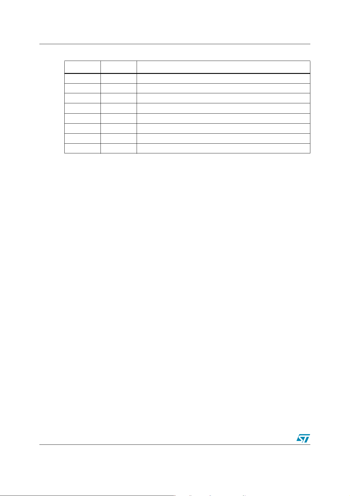
Date Revision Changes
26-Sep-2005 1 Initial release.
16/17 CD00068420

LIS2L02AL
Information furnished is believed to be accurate and reliable. However, STMicroelectronics assumes no responsibility for the consequences
of use of such information nor for any infringement of patents or other rights of third parties which may result from its use. No license is granted
by implication or otherwise under any patent or patent rights of STMicroelectronics. Specifications mentioned in this publication are subject
to change without notice. This publication supersedes and replaces all information previously supplied. STMicroelectronics products are not
authorized for use as critical components in life support devices or systems without express written approval of STMicroelectronics.
The ST logo is a registered trademark of STMicroelectronics.
All other names are the property of their respective owners
© 2005 STMicroelectronics - All rights reserved
STMicroelectronics group of companies
Australia - Belgium - Brazil - Canada - China - Czech Republic - Finland - France - Germany - Hong Kong - India - Israel - Italy - Japan -
Malaysia - Malta - Morocco - Singapore - Spain - Sweden - Switzerland - United Kingdom - United States of America
www.st.com
CD00068420 17/17
 Loading...