

LD2981
SERIES
ULTRA LOW DROP VOLTAGE REGULATORS WITH INHIBIT
LOW ESR OUTPUT CAPA CITORS COMPATIBLE
■ STABLE WITH LOW ESR CERAMIC
CAPACITORS
■ ULTRA LOW DROPOUT VOLTAGE (0.17V
TYP. AT 100m A LOAD, 7mV TYP. AT 1m A
LOAD)
■ VERY LOW QUIESCENT CURRENT (80µA
TYP. AT NO LOAD IN ON MODE; MAX 1µA
IN OFF MODE)
■ GUARANTEED OUTPUT CURRENT UP TO
100mA
■ LOGIC-CONTROLLED ELECTRONIC
SHUTDOWN
■ OUTPUT VOLTAGE OF 1.5; 1.8; 2.5; 2.85;
3.0; 3.2; 3.3; 3.6; 3.8; 4.0; 4.7; 4.85; 5.0V
■ INTERNAL CURRENT AND THERMAL LIMIT
■ ± 0.75% TOLERANCE OUTPUT VOLTAGE
AVAILABLE (A VERSION)
■ OUTPUT LOW NOISE VOLTAGE 160µVRM S
■ TEMPERATURE RANGE: -40 TO 125°C
■ SMALLEST PACKAGE SOT23-5L AND
SOT-89
■ FAST DYNAMIC RESPONSE TO LINE AND
LOADCHANGES
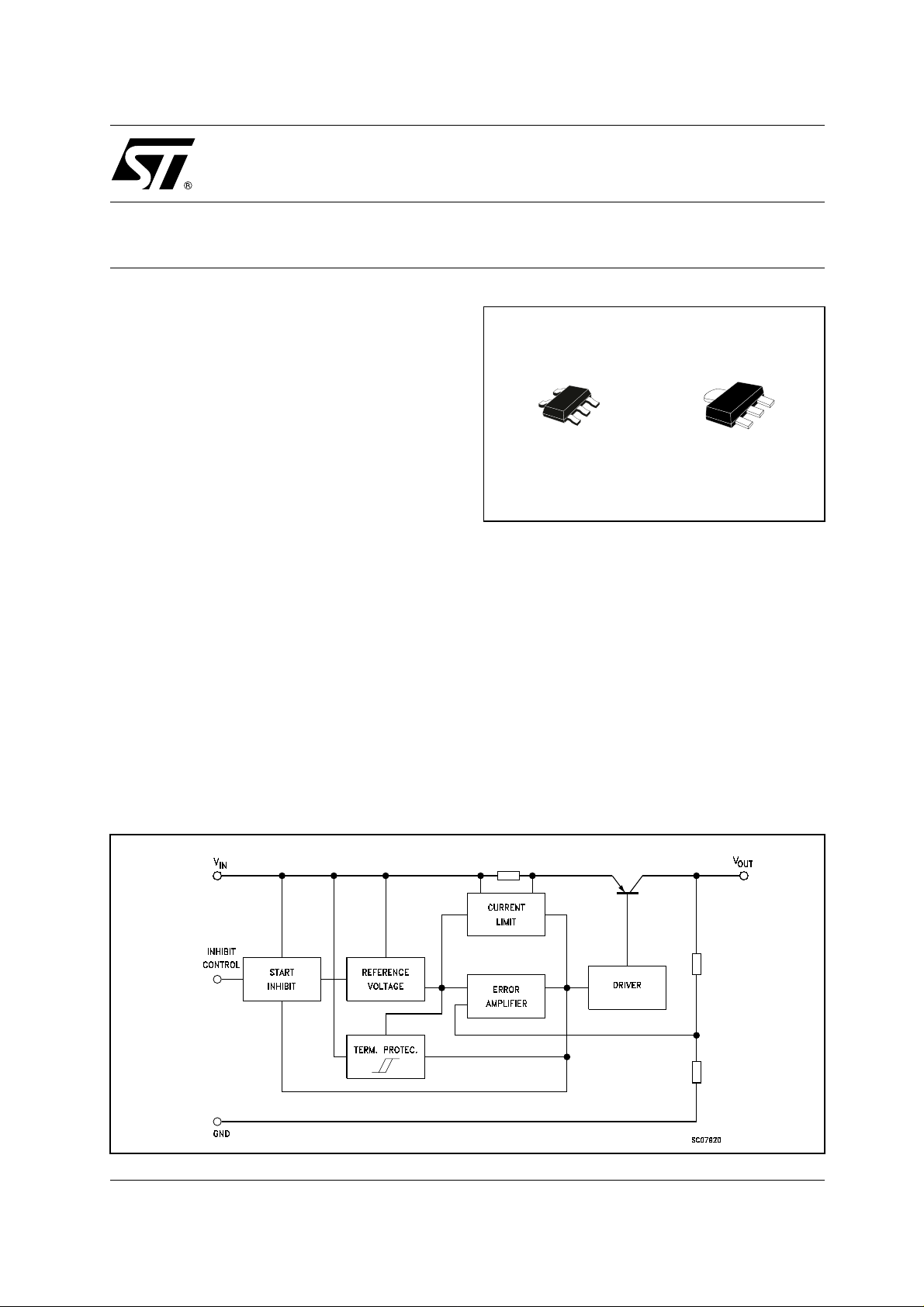
DESCRIPTION
The LD2981 series are 100mA fixed-output
voltage regulator. The low drop-voltage and the
ultra l ow quiescent current make them suitable for
low noise, low power applications and in battery
powered systems.
The quiescent current in sleep mode is less than
1µA when INHIBIT pin is pulled low. Shutdown
Logic Control function is available on pin n.3 (TTL
compatible). This means that when the device is
used as local regulator, it is possible to put a part
of the board in standby, decreasing the total
power consum ption. The LD2981 is designed to
work with l ow ESR ceramic capacitor. Typical
applications are in cellular phone, palmtop/laptop
computer, personal digital assistant (PDA),
personal stereo, camcorder and camera.
SOT23-5L SOT-89
SCHEMATIC DIAGRAM
1/17September 2003
LD2981 SERIES
ABSOLUTE MAXIMUM RATINGS
Symbol Parameter Value Unit
V
V
INH
I
P
T
STG
T
Absolute Maximum Ratings are those values beyond which damage to the device may occur. Functional operation under these condition is
not implied.
THERMAL DATA
Symbol Parameter SOT23-5L SOT-89 Unit
R
thj-case
R
thj-amb
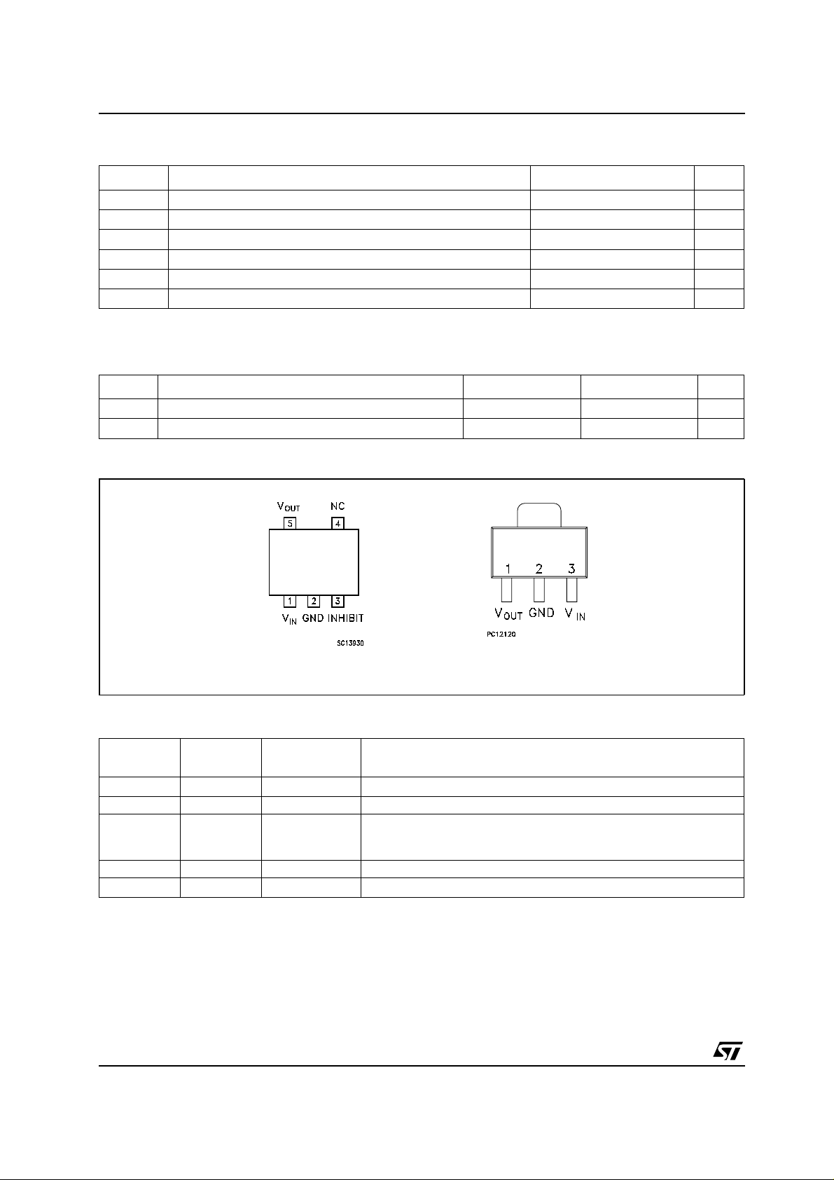
CONNECTION DIAGRAM (top view)
DC Input Voltage
I
INHIBIT Input Voltage
Output Current
O
Power Dissipation
D
Storage Temperature Range
Operating Junction Temperature Range
OP
Thermal Resistance Junction-case
Thermal Resistance Junction-ambient
-0.3 to 16 V
-0.3 to 16 V
Internally limited
Internally limited
-55 to 150 °C
-40 to 125 °C
81 15 °C/W
255 110 °C/W
SOT23-5L SOT-89
PIN DESCRIPTION
Pin N°
SOT23-5L
13 V
2 2 GND Ground Pin
3 INHIBIT Control switch ON/OFF. Inhibit is not internally pulled-up; it cannot be
4 NC Not Connected
51V
2/17
Pin N°
SOT-89
Symbol Name and Function
IN
Input Port
left floating. Disable the device when connected to GND or to a
positive voltage less than 0.18V
OUT
Output Port
ORDERING CODES
LD2981 SERIES
AB VERSION C VERSION
SOT23-5L SOT-89 SOT23-5L SOT-89
LD2981CM15TR LD2981CU15TR 1.5 V
LD2981CM18TR LD2981CU18TR 1.8 V
LD2981ABM25TR LD2981ABU25TR LD2981CM25TR LD2981CU25TR 2.5 V
LD2981ABM28TR LD2981ABU28TR LD2981CM28TR LD2981CU28TR 2.85 V
LD2981ABM30TR LD2981ABU30TR LD2981CM30TR LD2981CU30TR 3.0 V
LD2981ABM32TR LD2981ABU32TR LD2981CM32TR LD2981CU32TR 3.2 V
LD2981ABM33TR LD2981ABU33TR LD2981CM33TR LD2981CU33TR 3.3 V
LD2981ABM36TR LD2981ABU36TR LD2981CM36TR LD2981CU36TR 3.6 V
LD2981ABM38TR LD2981ABU38TR LD2981CM38TR LD2981CU38TR 3.8 V
LD2981ABM40TR LD2981ABU40TR LD2981CM40TR LD2981CU40TR 4.0 V
LD2981ABM47TR LD2981ABU47TR LD2981CM47TR LD2981CU47TR 4.7 V
LD2981ABM48TR LD2981ABU48TR LD2981CM48TR LD2981CU48TR 4.85 V
LD2981ABM50TR LD2981ABU50TR LD2981CM50TR LD2981CU50TR 5.0 V
VOLTAGES
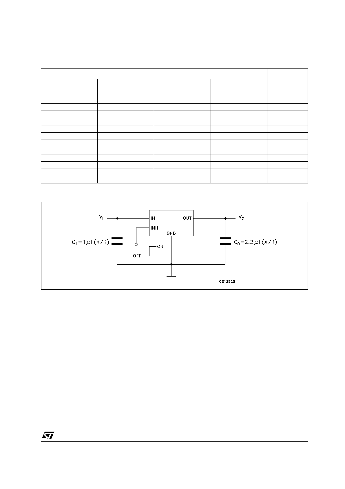
TYPICAL AP PLICATION CIRCUIT
OUTPUT
(*) Inhibit Pin is not internally pulled-up then it must not be left floating. Disable the device when connected to GND or to a positive voltage
less than 0.18V.
3/17
LD2981 SERIES
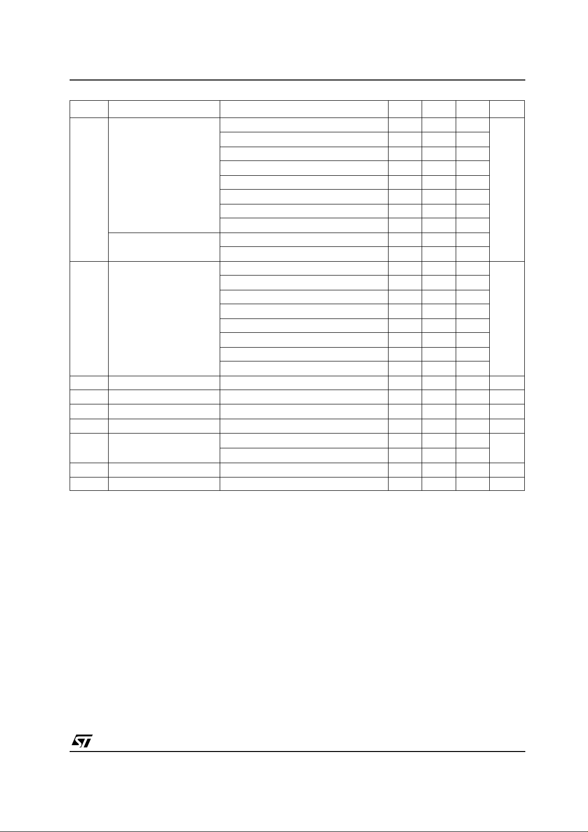
ELECTRICAL CHARACTERISTICS FOR LD2981AB (Tj= 25°C, VI=V
C
=2.2µF(X7R), IO=1mA,V
O
= 2V, unless otherwise specified)
INH
O(NOM)
+1V, CI=1µF(X7R),
Symbol Parameter Test Conditions Min. Typ. Max. Unit
V
Operating Input Voltage 2.5 16 V
OP
Output Voltage IO= 1 mA 2.481 2.5 2.518 V
V
O
= 1 to 100 mA 2.475 2.525
I
O
I
= 1 to 100 mA TJ= -40 to 125°C
O
V
Output Voltage IO= 1 mA 2.828 2.85 2.872 V
O
= 1 to 100 mA 2.822 2.878
I
O
I
= 1 to 100 mA TJ= -40 to 125°C
O
V
Output Voltage IO= 1 mA 2.977 3 3.023 V
O
= 1 to 100 mA 2.970 3.030
I
O
I
= 1 to 100 mA TJ= -40 to 125°C
O
V
Output Voltage IO= 1 mA 3.176 3.2 3.224 V
O
= 1 to 100 mA 3.168 3.232
I
O
I
= 1 to 100 mA TJ= -40 to 125°C
O
V
Output Voltage IO= 1 mA 3.275 3.3 3.325 V
O
= 1 to 100 mA 3.267 3.333
I
O
IO= 1 to 100 mA TJ= -40 to 125°C
V
Output Voltage IO= 1 mA 3.573 3.6 3.627 V
O
= 1 to 100 mA 3.564 3.636
I
O
I
= 1 to 100 mA TJ= -40 to 125°C
O
V
Output Voltage IO= 1 mA 3.771 3.8 3.829 V
O
= 1 to 100 mA 3.762 3.838
I
O
I
= 1 to 100 mA TJ= -40 to 125°C
O
V
Output Voltage IO= 1 mA 3.97 4 4.03 V
O
= 1 to 100 mA 3.96 4.04
I
O
I
= 1 to 100 mA TJ= -40 to 125°C
O
V
Output Voltage IO= 1 mA 4.664 4.7 4.735 V
O
= 1 to 100 mA 4.653 4.747
I
O
= 1 to 100 mA TJ= -40 to 125°C
I
O
V
Output Voltage IO= 1 mA 4.813 4.85 4.887 V
O
= 1 to 100 mA 4.801 4.899
I
O
I
= 1 to 100 mA TJ= -40 to 125°C
O
V
Output Voltage IO= 1 mA 4.962 5 5.038 V
O
= 1 to 100 mA 4.950 5.050
I
O
I
= 1 to 100 mA TJ= -40 to 125°C
O
∆V
Line Regulation V
O
T
+1<VIN<16V IO= 1 mA 0.003 0.014 %/V
O(NOM)
= -40 to 125°C
J
2.437 2.562
2.779 2.921
2.925 3.075
3.12 3.28
3.217 3.383
3.510 3.690
3.705 3.895
3.9 4.1
4.582 4.817
4.729 4.971
4.875 5.125
0.032
4/17
LD2981 SERIES
Symbol Parameter Test Conditions Min. Typ. Max. Unit
I
Quiescent Current
Q
ON MODE
OFF MODE V
V
Dropout Voltage (NOTE 1) IO=0 1 3 mV
DROP
I
Short Circuit Current RL= 0 150 mA
SC
SVR Supply Voltage Rejection C
V
T
(NOTE 1): For Vo < 2.5V dropout voltage can be calculated according to the minimum input voltage in full temperature range.
Inhibit Input Logic Low
INH
V
Inhibit Input Logic High
INL
Inhibit Input Current
I
INH
e
Output Noise Voltage BW= 300 Hz to 50 KHz CO=10µF 160 µV
N
Thermal Shutdown 170 °C
SHDN
IO= 0 80 100 µA
=0 TJ= -40 to 125°C
I
O
I
= 1 mA 100 150
O
IO=1mA TJ= -40 to 125°C
I
= 25 mA 250 400
O
IO=25mA TJ= -40 to 125°C
I
= 100 mA 1000 1300
O
= 100 mA TJ= -40 to 125°C
I
O
< 0.3 V 0.8
INH
< 0.15 V TJ= -40 to 125°C
V
INH
I
=0 TJ= -40 to 125°C
O
=1mA 7 10
I
O
I
=1mA TJ= -40 to 125°C
O
= 25mA 70 100
I
O
I
= 25mA TJ= -40 to 125°C
O
= 100mA 180 250
I
O
I
= 100mA TJ= -40 to 125°C
O
=10µFf=1KHz 63 dB
O
LOW = Output OFF T
HIGH = Output ON T
V
=0V TJ= -40 to 125°C
INH
=5V TJ= -40 to 125°C
V
INH
= -40 to 125°C
J
= -40 to 125°C
J
1.6 V
150
200
800
2600
2
5
15
150
375
0.18 V
0-1µA
515
RMS
5/17
LD2981 SERIES
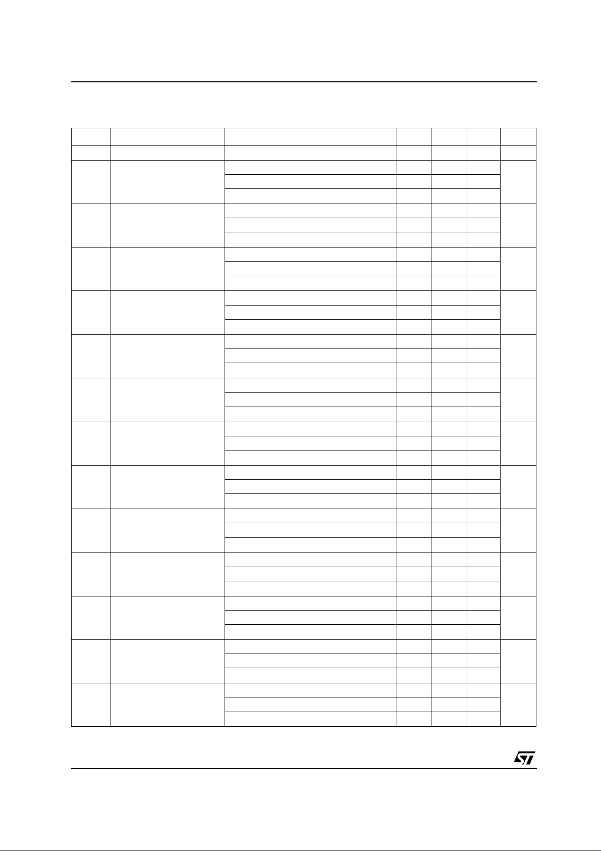
ELECTRICAL CHARACTERISTICS FOR LD2981C (Tj= 25°C, VI=V
C
=2.2µF(X7R), IO=1mA,V
O
= 2V, unless otherwise specified)
INH
O(NOM)
+1V, CI=1µF(X7R),
Symbol Parameter Test Conditions Min. Typ. Max. Unit
V
Operating Input Voltage 2.5 16 V
OP
Output Voltage IO= 1 mA 1.478 1.5 1.522 V
V
O
= 1 to 100 mA 1.470 1.530
I
O
I
= 1 to 100 mA TJ= -40 to 125°C
O
V
Output Voltage IO= 1 mA 1.777 1.8 1.822 V
O
= 1 to 100 mA 1.764 1.836
I
O
I
= 1 to 100 mA TJ= -40 to 125°C
O
V
Output Voltage IO= 1 mA 2.468 2.5 2.531 V
O
= 1 to 100 mA 2.45 2.55
I
O
I
= 1 to 100 mA TJ= -40 to 125°C
O
V
Output Voltage IO= 1 mA 2.814 2.85 2.885 V
O
= 1 to 100 mA 2.793 2.907
I
O
I
= 1 to 100 mA TJ= -40 to 125°C
O
V
Output Voltage IO= 1 mA 2.962 3 3.037 V
O
= 1 to 100 mA 2.94 3.06
I
O
IO= 1 to 100 mA TJ= -40 to 125°C
V
Output Voltage IO= 1 mA 3.16 3.2 3.24 V
O
= 1 to 100 mA 3.136 3.264
I
O
I
= 1 to 100 mA TJ= -40 to 125°C
O
V
Output Voltage IO= 1 mA 3.258 3.3 3.341 V
O
= 1 to 100 mA 3.234 3.366
I
O
I
= 1 to 100 mA TJ= -40 to 125°C
O
V
Output Voltage IO= 1 mA 3.555 3.6 3.645 V
O
= 1 to 100 mA 3.528 3.672
I
O
I
= 1 to 100 mA TJ= -40 to 125°C
O
V
Output Voltage IO= 1 mA 3.752 3.8 3.847 V
O
= 1 to 100 mA 3.724 3.876
I
O
= 1 to 100 mA TJ= -40 to 125°C
I
O
V
Output Voltage IO= 1 mA 3.95 4 4.05 V
O
= 1 to 100 mA 3.92 4.08
I
O
I
= 1 to 100 mA TJ= -40 to 125°C
O
V
Output Voltage IO= 1 mA 4.641 4.7 4.758 V
O
= 1 to 100 mA 4.606 4.794
I
O
I
= 1 to 100 mA TJ= -40 to 125°C
O
V
Output Voltage IO= 1 mA 4.789 4.85 4.91 V
O
= 1 to 100 mA 4.753 4.947
I
O
I
= 1 to 100 mA TJ= -40 to 125°C
O
V
Output Voltage IO= 1 mA 4.937 5 5.062 V
O
= 1 to 100 mA 4.9 5.1
I
O
I
= 1 to 100 mA TJ= -40 to 125°C
O
1.445 1.555
1.737 1.863
2.412 2.587
2.75 2.949
2.895 3.105
3.088 3.312
3.184 3.415
3.474 3.726
3.667 3.933
3.86 4.14
4.535 4.864
4.68 5.019
4.825 5.175
6/17
LD2981 SERIES
Symbol Parameter Test Conditions Min. Typ. Max. Unit
∆VOLine Regulation V
T
I
Quiescent Current
Q
ON MODE
IO= 0 80 100 µA
IO=0 TJ= -40 to 125°C
I
O
IO=1mA TJ= -40 to 125°C
I
O
I
O
I
O
I
O
OFF MODE V
V
V
Dropout Voltage (NOTE 1) IO=0 1 3 mV
DROP
I
O
I
O
I
O
I
O
I
O
IO= 100mA 180 250
I
O
I
Short Circuit Current RL= 0 150 mA
SC
SVR Supply Voltage Rejection C
V
Inhibit Input Logic Low
INH
V
Inhibit Input Logic High
INL
Inhibit Input Current
I
INH
LOW = Output OFF T
HIGH = Output ON T
V
V
e
Output Noise Voltage BW= 300 Hz to 50 KHz CO=10µF 160 µV
N
T
(NOTE 1): For Vo < 2.5V dropout voltage can be calculated according to the minimum input voltage in full temperature range.
Thermal Shutdown 170 °C
SHDN
+1<VIN<16V IO= 1 mA 0.003 0.014 %/V
O(NOM)
= -40 to 125°C
J
0.032
150
= 1 mA 100 150
200
= 25 mA 250 400
=25mA TJ= -40 to 125°C
800
= 100 mA 1000 1300
= 100 mA TJ= -40 to 125°C
< 0.3 V 0.8
INH
< 0.15 V TJ= -40 to 125°C
INH
=0 TJ= -40 to 125°C
2600
2
5
=1mA 7 10
=1mA TJ= -40 to 125°C
15
= 25mA 70 100
= 25mA TJ= -40 to 125°C
= 100mA TJ= -40 to 125°C
=10µFf=1KHz 63 dB
O
= -40 to 125°C
J
1.6 V
=0V TJ= -40 to 125°C
INH
=5V TJ= -40 to 125°C
INH
= -40 to 125°C
J
150
375
0.18 V
0-1µA
515
RMS
7/17

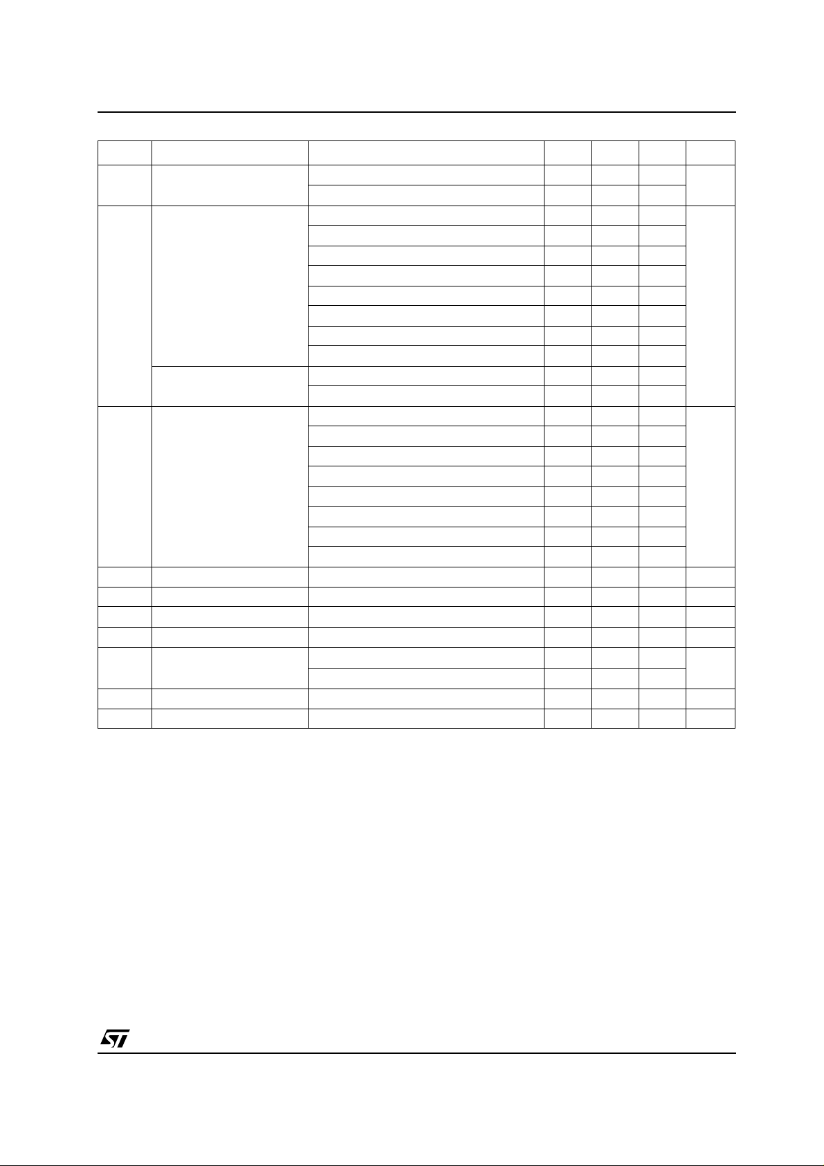
LD2981 SERIES
TYPICAL PERFORMANCE CHARACT ERISTICS (Tj= 25°C, VI=V
C
=2.2µF(X7R), V
O
Figure1 : Output Voltage vs Temperature
Figure2 : Output Voltage vs Temperature
= 2V, unless otherwise specified)
INH
Figure4 : Load Regulation vs Temperature
Figure5 : Dropout Voltage vs Temperature
O(NOM)
+1V, CI=1µF(X7R),
Figure3 : Line Regulation vs Temperature
8/17
Figure6 : Quiescent Current vs Temperature

LD2981 SERIES
Figure7 : Quiescent Current vs Output
Current
Figure8 : OFF MODE Quiescent Current vs
Temperature
Figure10 : Dropout Voltage vs Output Current
Figure11 : Inhibit Input Current vs Temperatu re
Figure9 : Quiescent Current vs Input Voltage
Figure12 : Inhibit Voltage vs Temperature
9/17

LD2981 SERIES
V
I
100mA,C
R
V
(V
1V),V
I
100mA,C
R
Figure13 : Supply Voltage Rejection vs
Frequency
Figure14 : Noise Voltage vs Frequency
Figure16 : Worst Case: Lowest Output Version
Figure17 : Load Transient Response
Figure15 : Best Case: Highest Output V ers ion
10/17
=4.7V,
O
O
=1to
=4.7µFX7
O
Figure18 : Line Transient Response
=
I
O(NOM)
+
=4.7V,
O
=
O
O
=4.7µFX7

LD2981 SERIES
APPLICATION NOTES
EXTERNAL CAPACITORS
Like a ny low-dropout regulator, the LD2981 requires external capacitors for regulator stability. This
capacitor must be selected to meet the requirements of minimum capacitance and equiva lent series
resistance. We s uggest to solder input and output capacitors as close as possible to the relative pins.
INPUT CAP ACITOR
An input capacitor whose value is 1µF is required with the LD2981 (amount of capacitance can be
increased wit hout limit). This capacitor must be located a distance of not more t han 0.5" from the input pi n
of the d ev ice and returned to a clean analog ground. Any good quality ceramic, tant alum or film capacitors
can be used for this capacitor.
OUTPUT CAPACITOR
The LD2981 is designed specifically to workwith ceramic output capacitors. It may also be possible to use
Tantalum capacitors, but these are not as attractive for reasons of size and cost. By the way, the output
capacitor must meet both the requirement for minimum amount of capacitance and ESR (equivalent
series resistance) value. Th e f igures 1 and 2 show the allowable ESR range as a function of the output
capacitance. These curves represent the stability region over the full temperature and I
the different loop gain, the stability improves for higher output versions and so t he suggested minimum
output capacitor value, if low ESR ceramic type is used, is 1µF for output voltages equal or major than
3.8V, 2.2µF for output voltages from 2.85 to 3.3V, a nd 3.3µF for the other v ersions. However, if an output
capacitor lower than the suggested one isused, it’s possible t o make stable the re gulator adding a resistor
in series to the capacitor (see Figure1 & Figure2 to choose the right value according to the us ed ve rsion
and keeping in account that the E SR of ceramic capacitors has been measured @ 100KHz).
range. Due to
O
IMPORTANT
The output capacitor must maintain its ESR in the stable region over the full op erating temperature to
assure stability. Also, capacitor tolerance and variation with temperature must be considered to assure
the minimum amount of capacit anc e is provided at all times. This capa citor should be located not more
than 0.5" from the output pin of the device and returned to a clean analog ground.
INHIBIT INPUT OPERATION
The inhibit pin can be us ed to turn OFF the regulator when pulled low, so drastically reducing the current
consumption down to less than 1µA. Whe n the inhibit feature is not used, this pin mus t be tied to V
to
I
keep the regulator output ON at all times. To as s ure proper operation, the signal source used to drive the
inhibit pin must be able to swing above and below the spec if ied thresholds listed in the electrical
characteristics section under V
.Anyslewratecanbeusedtodrivetheinhibit.
IHVIL
REVERSE CURRENT
The power trans istor used in the LD2981 has not an inherent diode connected between the regulator input
and output. If the output is forced above th e input, no current will flow from the output to the input across
the series pass transistor. When a V
voltage is applied on the output, the reverse current meas ured,
REV
according to the test c ircuit in figure 19, flows to the GND across the two feedback res isto rs. This current
typical value is 160µA. R
and R2resistors are implanted type; typical values are, res pectively, 42.6 KΩ
1
and 51.150 KΩ.
11/17

LD2981 SERIES
Figure19 : Reverse Current Test Circuit
12/17

LD2981 SERIES
SOT23-5L MECHANICAL DATA
mm. mils
DIM.
MIN. TYP MAX. MIN. TYP. MAX.
A 0.90 1.45 35.4 57.1
A1 0.00 0.10 0.0 3.9
A2 0.90 1.30 35.4 51.2
b 0.35 0.50 13.7 19.7
C 0.09 0.20 3.5 7.8
D 2.80 3.00 110.2 118.1
E 1.50 1.75 59.0 68.8
e0.95 37.4
H 2.60 3.00 102.3 118.1
L 0.10 0.60 3.9 23.6
.
7049676C
13/17

LD2981 SERIES
SOT-89 MECHANICAL DATA
mm. mils
DIM.
MIN. TYP MAX. MIN. TYP. MAX.
A 1.4 1.6 55.1 63.0
B 0.44 0.56 17.3 22.0
B1 0.36 0.48 14.2 18.9
C 0.35 0.44 13.8 17.3
C1 0.35 0.44 13.8 17.3
D 4.4 4.6 173.2 181.1
D1 1.62 1.83 63.8 72.0
E 2.29 2.6 90.2 102.4
e 1.42 1.57 55.9 61.8
e1 2.92 3.07 115.0 120.9
H 3.94 4.25 155.1 167.3
L 0.89 1.2 35.0 47.2
14/17
P025H

Tape & Reel SOT23-xL MECHANICAL DATA
LD2981 SERIES
DIM.
MIN. TYP MAX. MIN. TYP. MAX.
A 180 7.086
C 12.8 13.0 13.2 0.504 0.512 0.519
D 20.2 0.795
N 60 2.362
T 14.4 0.567
Ao 3.13 3.23 3.33 0.123 0.127 0.131
Bo 3.07 3.17 3.27 0.120 0.124 0.128
Ko 1.27 1.37 1.47 0.050 0.054 0.0.58
Po 3.9 4.0 4.1 0.153 0.157 0.161
P 3.9 4.0 4.1 0.153 0.157 0.161
mm. inch
15/17

LD2981 SERIES
Tape & Reel SOT89 ME CHANICA L DATA
DIM.
MIN. TYP MAX. MIN. TYP. MAX.
A 180 7.086
C 12.8 13.0 13.2 0.504 0.512 0.519
D 20.2 0.795
N 60 2.362
T 14.4 0.567
Ao 4.70 4.80 4.90 0.185 0.189 0.193
Bo 4.30 4.40 4.50 0.169 0.173 0.177
Ko 1.70 1.80 1.90 0.067 0.071 0.075
Po 3.9 4.0 4.1 0.153 0.157 0.161
P 7.9 8.0 8.1 0.311 0.315 0.319
mm. inch
16/17

LD2981 SERIES
Information furnished is believed to be accurate and reliable. However, STMicroelectronics assumes no responsibility for the
consequences of use o f suc h info rmat ion n or for any in fring ement of paten ts or oth er ri ghts of th ird p arties which may resul t f rom
its use. No license is granted by implication or otherwise under any patent or patent rights of STMicroelectronics. Specifications
mentioned in this publication are subject to change without notice. This publication supersedes and replaces all information
previously supplied. STMicroelectronics products are not authorized for use as critical components in life support devices or
systems without express written approval of STMicroelectronics.
Australia - Belgium - Brazil - Canada - China - Czech Republic - Finland - France - Germany - Hong Kong - India - Israel - Italy - Japan -
Malaysia - Malta - Morocco - Singapore - Spain - Sweden - Switzerland - United Kingdom - United States.
The ST logo is a registered trademark of STMicroelectronics
All other names are the property of their respective owners
© 2003 STMicroelectronics - All Rights Reserved
STMicroelectronics GROUP OF COMPANIES
http://www.st.com
17/17
 Loading...