

Page 1
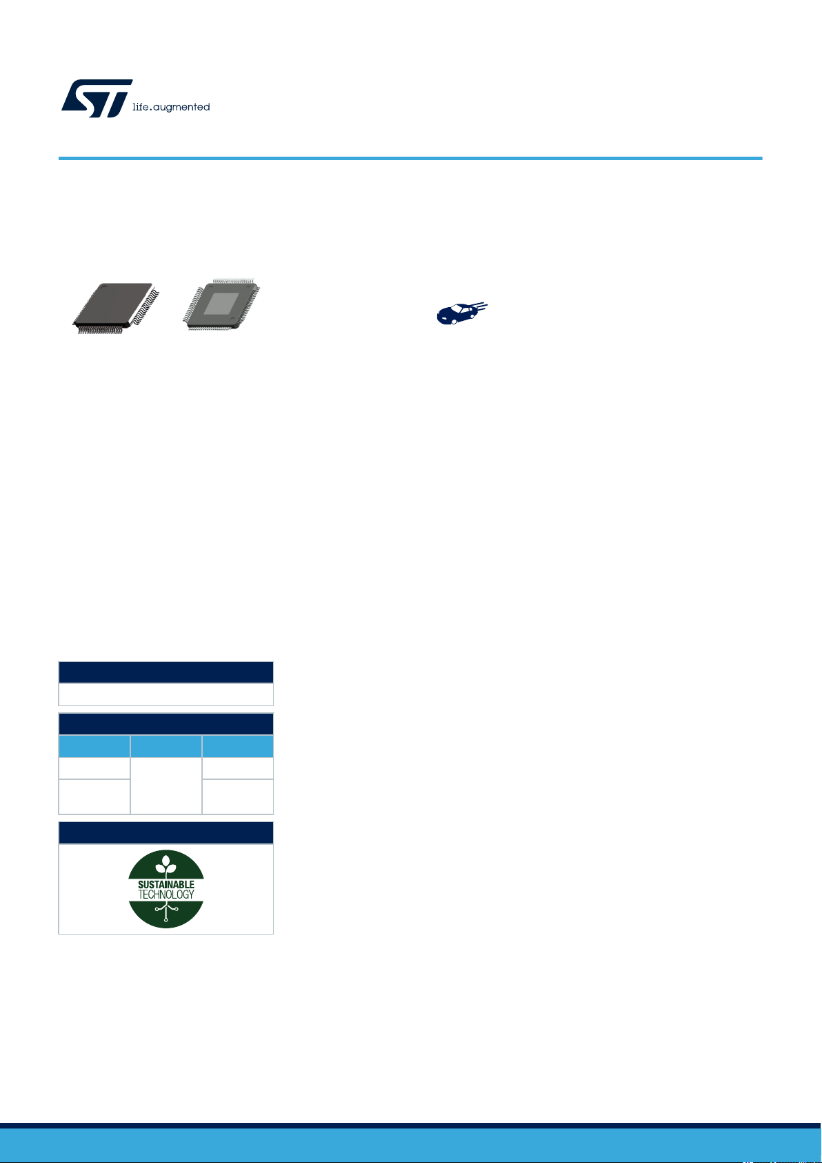
TQFP 10x10 64L
exposed pad down
Product status link
L9963E
Product summary
Order code Package Packing
L9963E
L9963E-TR
TQFP64EP
Product label
Tray
Tape and
Reel
L9963E
Datasheet
Automotive Multicell battery monitoring and balancing IC
Features
• AEC-Q100 qualified
• Measures 4 to 14 cells in series, with 0 μs desynchronization delay between
samples. Supports also busbar connection without altering cell results
• Coulomb counter supporting pack overcurrent detection in both ignition on and
off states. Fully synchronized current and voltage samples
• 16-bit voltage ADC with maximum error of ±2 mV in the [0.5 – 4.3] V range, after
soldering, in [-40; +105] °C Tj range
• 2.66 Mbps isolated serial communication with regenerative buffer, supporting
dual access ring. Less than 4 us latency between start of conversion of the 1st
and the 31st device in a chain. Less than 4 ms to convert and read 96 cells in a
system using 8 L9963E and L9963T transceiver. Less than 8 ms to convert and
read 210 cells in a system using 15 L9963E and L9963T transceiver. Less than
16 ms to convert and read 434 cells in a system using 31 L9963E and L9963T
transceiver. Supports both XFMR and CAP based isolation
• 200 mA passive internal balancing current for each cell in both normal and
silent-balancing mode. Possibility of executing cyclic wake up measurements.
Manual/Timed balancing, on multiple channels simultaneously; Internal/External
balancing
• Fully redundant cell measurement path, with ADC Swap, for enhanced safety
and limp home functionality
• Intelligent diagnostic routine providing automatic failure validation. Redundant
fault notification through both SPI Global Status Word (GSW) and dedicated
FAULT line
• Two 5 V regulators supporting external load connection with 25 mA (VCOM) and
50 mA (VTREF) current capability
• 9 GPIOs, with up to 7 analog inputs for NTC sensing
• Robust hot-plug performance. No Zeners needed in parallel to each cell
• Full ISO26262 compliant, ASIL-D systems ready
Application
• Automotive: 48 V and high-voltage battery packs
• Backup energy storage systems and UPS
• E-bikes, e-scooters
• Portable and semi-portable equipment
Description
The L9963E is a Li-ion battery monitoring and protecting chip for high-reliability
automotive applications and energy storage systems. Up to 14 stacked battery cells
can be monitored to meet the requirements of 48 V and higher voltage systems.
Each cell voltage is measured with high accuracy, as well as the current for the
on-chip coulomb counting. The device can monitor up to 7 NTCs. The information is
transmitted through SPI communication or isolated interface.
DS13636 - Rev 3 - April 2021
For further information contact your local STMicroelectronics sales office.
www.st.com
Page 2

L9963E
Multiple L9963E can be connected in a daisy chain and communicate with one host
processor via the transformer isolated interfaces, featuring high-speed, low EMI, long
distance, and reliable data transmission.
Passive balancing with programmable channel selection is offered in both normal
and low power mode (silent balance). The balancing can be terminated automatically
based on internal timer interrupt. Nine GPIOs are integrated for external monitoring
and controlling. The L9963E features a comprehensive set of fault detection and
notification functions to meet the safety standard requirements.
DS13636 - Rev 3
page 2/184
Page 3

1 Device introduction
The L9963E is intended for operation in both hybrid (HE) and full electric (FE) vehicles using lithium battery
packs. The IC embeds all the features needed to perform battery management. A single device can monitor from
4 up to 14 cells. Several devices can be stacked in a vertical arrangement in order to monitor up to 31 battery
packs for a total of 434 series cells.
The device can be supplied with the same battery it monitors, and generates stable internal references by
means of a voltage regulator and a bootstrap. Both unit need to be surrounded by external components to be
functional. It also features two internal bandgaps that are constantly monitored by internal circuitry to guarantee
measurement precision. The microcontroller can also monitor the precision of the bandgap by reading the
conversion of an internally generated voltage reference (VTREF).
L9963E main activity consists in monitoring cells and battery pack status through stack voltage measurement,
cell voltage measurement, temperature measurement and coulomb counting. Measurement and diagnostic tasks
can be executed either on demand or periodically, with a programmable cycle interval. Measurement data is
available for an external microcontroller to perform charge balancing and to compute the State Of Health (SOH)
and State Of Charge (SOC). In a typical use, the IC works in normal mode performing measurement conversions,
diagnostics and communication; the device can also be put into a cyclic wake up state, in order to reduce the
current consumption from the battery: while in this state, the main functions are activated periodically.
Passive cell balancing can be performed either via internal discharge path or via external MOSFETs. The
controller can either manually control the balancing drivers or start a balancing task with a fixed duration. In
the second case, the balancing may be programmed to continue also when the IC enters a low power mode
called Silent Balancing, in order to avoiding unnecessary current absorption from the battery pack.
Thanks to the GPIOs, the device also offers the possibility to operate a distributed cell temperature sensing via
external NTCs resistances. In general, the GPIOs can be used to perform both absolute and differential voltage
conversions. They can also be configured as digital inputs/outputs. The IC supports up to 7 NTCs.
The external microcontroller can communicate with L9963E via SPI protocol, depending on the status of one pin
at the startup (SPIEN pin). The physical layer can be either a classical 4-wire based SPI or a 2-wire, transformer/
capacitive based, isolated interface through a dedicated isolated transceiver device. L9963E, in fact, can be used
as a transceiver, acting as a bridge between the two physical layers. In case of multiple L9963E vertically arrayed,
each L9963E communicates with the others by means of a vertical isolated interface. The microcontroller can
either address a single device of the chain or send broadcast commands.
L9963E has been engineered to perform automatic validation of any failure involving the cells or the whole battery
pack. The device is able to detect the loss of the connection to a cell or GPIO terminal. Moreover it features an
HardWare Self Check (HWSC) that verifies the correct functionality of the internal analog comparators and the
ADCs. All these checks are automatically performed in case a failure involving both cells or the battery pack is
detected, in order to provide always a reliable information to the external microcontroller. The current sensing
interface used for coulomb counting is also capable of detecting failures such as open wires and overcurrent in
sleep mode. Conversions for coulomb counting are validated by built in self-test of the precision and detecting
any counter overflow. The cell balancing terminals can detect any short/open fault and the internal powerMOS are
protected against overcurrent.
The stack voltage is monitored for OV/UV by three parallel and independent system. They have been engineered
to protect the IC against AMR violation, to detect any overvoltage event as per LV 148 and to provide the
possibility to trim the OV/UV levels according to the application and the total number of cells. Moreover, all
internal voltage regulators are equipped with UV/OV detection circuitry, that is also self-validated upon failure
detection via HWSC. Ground loss detection has also been implemented. In case of overtemperature, thermal
shutdown protects the IC. GPIOs are capable of detecting ‘stuck @’ faults when used as digital outputs.
Communication integrity is guaranteed by CRC check, while trimming and calibration data is continuously
checked against corruption. Protocol errors such as incorrect address, inconsistent frame and communication
interruption will be detected.
Critical failure modes will trigger the assertion of a dedicated FAULT line (implemented via two GPIOs),
propagating through the L9963E chain via external optocouplers and reaching the microcontroller. L9963E can
guarantee the FAULT line integrity via a heartbeat routine.
L9963E
Device introduction
DS13636 - Rev 3
page 3/184
Page 4

Figure 1. Typical application
L9963E
VBAT
GNDREF
CGND
DGND
AGND
ISENSEp
ISENSEm
RSENSE
S2
B2_1
C1
S1
C0
RLPF
RLPF
RDIS
RDIS
CLPF
CLPF
CESD
CESD
CELL1
CELL2
C14
S4
B4_3
C3
S3
C2
RLPF
RLPF
RDIS
RDIS
CLPF
CLPF
CESD
CESD
CELL3
CELL4
S6
B6_5
C5
S5
C4
RLPF
RLPF
RDIS
RDIS
CLPF
CLPF
CESD
CESD
CELL5
CELL6
S8
B8_7
C7
S7
C6
RLPF
RLPF
RDIS
RDIS
CLPF
CLPF
CESD
CESD
CELL7
CELL8
S10
B10_9
C9
S9
C8
RLPF
RLPF
RDIS
RDIS
CLPF
CLPF
CESD
CESD
CELL9
CELL10
S12
B12_11
C11
S11
C10
RLPF
RLPF
RDIS
RDIS
CLPF
CLPF
CESD
CESD
CELL11
CELL12
S14
B14_13
C13
S13
C12
RLPF
RLPF
RDIS
RDIS
CLPF
CLPF
CESD
CESD
CELL13
CELL14
RLPF
CESD
FR_BAT
BATT_MINUS
BATT_PLUS
CISENSE_1
VTREF
NPNDRV
VREG
CREG
CBAT_1
VCOM
CVCOM
VANA
CVANA
SPIEN
FAULTL
RFAULTL
RBAT_DOWNRFAULT_DOWN
FAULT_DOWN BAT_DOWN
DOPT
RBAT_UP
BATT_UP
FAULTH
CFLTH
RFLT
DZ_FLT
RFLT_PD
FAULT_UP
ISOHp
ISOHm
ISOLp_UP ISOLm_UP
ISOLp
ISOLm
ISOHp_DOWN
ISOHm_DOWN
RTERM
RTERM
GPIO9
RNTC
RVTREF
CNTC
RGPIO
GPIO8
RNTC
RVTREF
CNTC
RGPIO
GPIO7
RNTC
RVTREF
CNTC
RGPIO
GPIO6
RNTC
RVTREF
CNTC
RGPIO
GPIO5
RNTC
RVTREF
CNTC
RGPIO
GPIO4
RNTC
RVTREF
CNTC
RGPIO
GPIO3
RNTC
RVTREF
CNTC
RGPIO
CAP1
CAP2
CBOOT
MREG
TRANSF
TRANSF
OPT
DZBAT
CVTREF
CESD
RISENSE
RISENSE
CESD
CBAT_2
CISENSE_2
CISENSE_3
CNPN
CBAT_3
AGND
DGND
GND_ESD
PACK_GND
L9963E
Device introduction
DS13636 - Rev 3
page 4/184
Page 5

2 Block diagram and pin description
GADG1010180719PS
BOOTSTRAP
DGND
VBAT
CAP1
CAP2
c14
s14
b14_13
b12_11
c13
c11
c12
s13
s11
s2
c1
c2
c0
ISENSEp
ISENSEm
GNDREF
s1
b2_1
VBAT
AGND CGND
GNDREF
CGND
CGND
CGND
AGND
AGND
DGND
DGND
GNDREF
GNDREF
GNDREF
DGND
AGND
CGND
NPNDRV
NPNDRV
Ree
Digital
Control
&
Data
Register
VDIG
VANA
VCOM
ISO
SPI
GPIO
VTREF
CSA
DIAG
ADCs
VREG
VDIG
VANA
VANA
Bal CT
Bal CT
Bal CT
Bal CT
Bal CT
Bal CT
VANA
VCOM
VCOM
VCOM
VCOM
VANA
VDIG
VDIG
VTREF
VANA
VCOM
VTREF
SPIEN
GPIO9/SDO
GPIO8/SCK
GPIO7/WAKEUP
GPIO6
GPIO5
GPIO4
GPIO3
GPIO2/FAULTL
GPIO1/FAULTH
ISOHp
ISOHm
ISOLp/SDI
ISOLm/NCS
2.1 Block diagram
Figure 2. Block diagram
L9963E
Block diagram and pin description
DS13636 - Rev 3
page 5/184
Page 6

2.2 Pin description
L9963E
Pin description
Figure 3. Pin connections (top view)
DS13636 - Rev 3
Pin #
1 GPIO8_ SCK
2 GPIO9_ SDO
3 ISOLp_SDI
4 ISOLm_NCS
Pin name Description
Table 1. Pin function
General-purpose I/O / Serial clock input (SPI). Its configuration is locked to
Digital Input in case SPIEN = 1. Refer to Section 4.9 General purpose I/O:
GPIOs. Generally used to sense NTCs when not configured as SPI. Refer to
Section 6.9 NTC analog front end.
General-purpose I/O / Serial data output (SPI). Its configuration is locked to
Digital Output in case SPIEN = 1. Refer to Section 4.9 General purpose I/O:
GPIOs. Generally used to sense NTCs when not configured as SPI. Refer to
Section 6.9 NTC analog front end.
Non-inverting, low-side isolated serial communication port (isolated SPI) / Serial data
input (SPI). Its configuration is locked to Digital Input in case SPIEN = 1. Refer to
Section 4.2 Serial communication interface. When used as isolated SPI, refer to
Section 6.8 ISO lines circuit.
Inverting, low-side isolated serial communication port (isolated SPI) / Active low,
Chip-Select input (SPI). Its configuration is locked to Digital Input in case SPIEN =
1. Refer to Section 4.2 Serial communication interface. When used as isolated SPI,
refer to Section 6.8 ISO lines circuit.
I/O type
DO/DI/AI
DO/DI/AI
DI/AIO
DI/AIO
page 6/184
(1)
Page 7

L9963E
Pin description
Pin # Pin name Description
I/O type
Regulated power supply used for communication interfaces. Connect a tank
5 VCOM
capacitor as indicated in Table 73. Can be used to supply external loads with a
maximum I
VCOM_ext
current budget.
6 CGND Communication ground. Connect to DGND on top. G
Non-inverting, high-side isolated serial communication port. Refer to
7 ISOHp
Section 4.2.3 Isolated Serial Peripheral Interface. Refer to Section 6.8 ISO lines
AIO
circuit.
Inverting, high-side isolated serial communication port. Refer to
8 ISOHm
Section 4.2.3 Isolated Serial Peripheral Interface. Refer to Section 6.8 ISO lines
AIO
circuit.
9 DGND Digital ground. Connect to AGND on top. G
10 GPIO1_ FAULTH Digital input used for FAULTH receiver. Refer to Section 4.3 FAULT line. DI
11 GPIO2_ FAULTL Digital output used for FAULTL transmitter. Refer to Section 4.3 FAULT line. DO
12 GPIO3
13 GPIO4 AI/DI/DO
14 GPIO5 AI/DI/DO
General-purpose I/O. Refer to Section 4.9 General purpose I/O: GPIOs. Generally
used to sense NTCs. Refer to Section 6.9 NTC analog front end.
AI/DI/DO
15 GPIO6 AI/DI/DO
General-purpose I/O. Refer to Section 4.9 General purpose I/O: GPIOs. Generally
16 GPIO7_ WAKEUP
used to sense NTCs. Refer to Section 6.9 NTC analog front end. Can be
AI/DI/DO
configured to act as wake up input. Refer to Section 4.9.4 GPIO7: wake up feature.
17 NPNDRV
Internal voltage regulator controller output. Connect to the base of the external NPN
transistor.
AO
Regulated analog power supply for core circuitry. Connect a tank capacitor as
18 VREG
indicated in Table 73. It is disabled in low power modes (Silent Balancing, Sleep
and during the OFF phase of Cyclic Wakeup). VCOM, VANA and VTREF regulators
are fed by pre-regulated VREG.
19 VTREF
Buffered, precise analog reference voltage for driving multiple NTCs. Connect a tank
capacitor as indicated in Table 73. It has a maximum IVTREF_ext current budget.
At first power up, after VCOM is out of undervoltage, this pin is sampled to
20 SPIEN
determine port L configuration. Connect to VCOM to configure SPI mode. Connect
to AGND to select isolated SPI communication.
DI
If left floating, this pin has a 100KΩ internal Pull down, forcing isolated SPI mode.
21 VANA Precise ADC analog supply. Connect a tank capacitor as indicated in Table 73. P
22 AGND Analog/ESD ground. Ground supply of chip. G
23 ISENSEp Non-inverting input of current measurement. Refer to Table 73. AI
24 ISENSEm Inverting input of current measurement. Refer to Table 73. AI
25 GNDREF Analog/reference GND. Connect to AGND on top G
26 C0 Connect to the negative terminal of 1st cell. AI
27 C1 Cell voltage input. Connect to the positive terminal of 1st cell. AI
28 S1 Cell balancing FET control output for 1st cell. AO
29 B2_1 Common terminal for cell balancing S1 and S2. AO
30 S2 Cell balancing FET control output for 2nd cell. AO
31 C2 Cell voltage input. Connect to the positive terminal of 2nd cell. AI
32 C3 Cell voltage input. Connect to the positive terminal of 3rd cell. AI
33 S3 Cell balancing FET control output for 3rd cell. AO
34 B4_3 Common terminal for cell balancing S3 and S4. AO
35 S4 Cell balancing FET control output for 4th cell. AO
(1)
P
P
P
DS13636 - Rev 3
page 7/184
Page 8

L9963E
Pin description
Pin # Pin name Description
I/O type
36 C4 Cell voltage input. Connect to the positive terminal of 4th cell. AI
37 C5 Cell voltage input. Connect to the positive terminal of 5th cell. AI
38 S5 Cell balancing FET control output for 5th cell. AO
39 B6_5 Common terminal for cell balancing S5 and S6. AO
40 S6 Cell balancing FET control output for 6th cell. AO
41 C6 Cell voltage input. Connect to the positive terminal of 6th cell. AI
42 C7 Cell voltage input. Connect to the positive terminal of 7th cell. AI
43 S7 Cell balancing FET control output for 7th cell. AO
44 B8_7 Common terminal for cell balancing S7 and S8. AO
45 S8 Cell balancing FET control output for 8th cell. AO
46 C8 Cell voltage input. Connect to the positive terminal of 8th cell. AI
47 C9 Cell voltage input. Connect to the positive terminal of 9th cell. AI
48 S9 Cell balancing FET control output for 9th cell. AO
49 B10_9 Common terminal for cell balancing S9 and S10. AO
50 S10 Cell balancing FET control output for 10th cell. AO
51 C10 Cell voltage input. Connect to the positive terminal of 10th cell. AI
52 C11 Cell voltage input. Connect to the positive terminal of 11th cell. AI
53 S11 Cell balancing FET control output for 11th cell. AO
54 B12_11 Common terminal for cell balancing S11 and S12. AO
55 S12 Cell balancing FET control output for 12th cell. AO
56 C12 Cell voltage input. Connect to the positive terminal of 12th cell. AI
57 C13 Cell voltage input. Connect to the positive terminal of 13th cell. AI
58 S13 Cell balancing FET control output for 13th cell. AO
59 B14_13 Common terminal for cell balancing S13 and S14. AO
60 S14 Cell balancing FET control output for 14th cell. AO
61 C14 Cell voltage input. Connect to the positive terminal of 14th cell. AI
62 VBAT
Power supply of chip. This pin is also sensed by internal ADC through a voltage
divider. Refer to Table 73.
63 CAP2 Pin2 external bootstrap capacitance. Refer to Table 73. AI
64 CAP1 Pin1 external bootstrap capacitance. Refer to Table 73. AI
- GNDEP Ground terminal, connect to AGND plane G
1. I/O type legend: AI = Analog Input; AO = Analog Output; AIO = Analog I/O; DI = Digital Input; DO = DigitalOutput; DIO =
Digital I/O; P = Power; G = Ground; NC = Not Connect.
(1)
P
DS13636 - Rev 3
page 8/184
Page 9

3 Product electrical ratings
3.1 Operating range
Within the operating range the part operates as specified and without parameter deviations. The device may not
operate properly if maximum operating conditions are exceeded.
Once taken beyond the operative ratings and returned back within, the part will recover with no damage or
degradation, unless the AMR are exceeded.
Additional supply voltage and temperature conditions are given separately at the beginning of each electrical
specification table.
All voltages are related to the potential at substrate ground AGND, unless otherwise noted.
Symbol Parameter Test conditions Min. Typ. Max. Unit
VBAT Global
VBAT, VREG, VCOM, VTREF
C0 Global Lower Cell Terminal Voltage -0.3 0.3 V
B(n,n-1); Sn Global Cell Terminal Voltage 0 VBAT V
C(n) for n=1 to 9 Global Cell Terminal Voltage 0 VBAT – 4.5 V
C(n) for n=10 to 14 Global Cell Terminal Voltage 3 VBAT + 0.3 V
C(n)-C(n-1) for n=1 to 14 Cell Terminal Differential Voltage 0 4.7 V
S(n+1)-B(n+1,n); B(n+1,n)-S(n)
for n=1 to 13 odd
C(n)-S(n) for n=1 to 14 Cell Terminal Differential Voltage 0 4.7 V
VBAT – C(14)
ISOHP/M, ISOLP/M Global -0.3 VCOM V
GPIOn Local -0.3 VCOM V
SPIEN Local -0.3 VCOM V
VTREF Local 5 V
|ISENSEP – ISENSEM| Local
|ISENSEP + ISENSEM| / 2 Local
VCOM Local 5 V
VANA Local Info only 3.3 V
VREG Local 6.5 V
NPNDRV Local VREG-0.3 VREG + 1.5 V
CAP1 Local 0 VBAT V
CAP2 Local VREG VBAT + VREG V
L9963E
Product electrical ratings
Table 2. Operating ranges
Supply voltage 9.6 64 V
Transient operation, 40 ms pulse,
repetitive as per VDA320 E48-02
test.
Supply voltage in case of
transceiver use only (see
Section 6.12 Transceiver mode)
Cell Balance Terminal Differential
Voltage
Battery / high Terminal Differential
Voltage
CSA Input Differential Mode
Range
CSA Input Common Mode Range
(Referenced to GNDREF)
64 70 V
4.6 5 5.4 V
0 4.7 V
-0.3 61 V
-0.15 0.15 V
-0.225 0.225 V
DS13636 - Rev 3
page 9/184
Page 10

3.1.1 Supply voltage ranges
AMR
Violation
•Permanent
damage
•Permanent
parameter
deviation
Critical
UV
• Params may
deviate
• Balance
disabled
• Transceiver
usage
Dyn UV
•No
param
deviation
•All
functions
guarante
ed
Normal
Op
•All
functions
guarantee
d
Dyn OV
•Cell total
error
slightly
increased
•All
functions
guarantee
d
Critical
OV
•Params
may
deviate
•All
functions
available
AMR
Violation
•Permanent
damage
•Permanent
parameter
deviation
VBAT
- 0.3 V
5.4 V
4.6 V
9.6 V
12 V
64 V
70 V
72 V
The device operates up to 14 cells of battery for hybrid and electric vehicles. The device can cover the voltage
range of the main automotive Lithium batteries, up to a maximum of 4.6 V per cell in operating conditions. The IC
has been engineered to sustain transient OV events as per LV 148
All operative ranges are listed in picture below.
If the stand by V3V3 regulator goes in POR, the device is put in reset.
Figure 4. Device operation in the VBAT supply voltage ranges
L9963E
Absolute maximum ratings
3.2
Absolute maximum ratings
Exceeding any Absolute Maximum Rating (AMR) may cause permanent damage to the integrated circuit.
All voltages are related to the potential at substrate ground AGND.
Table 3. Absolute Maximum Rating
Symbol Parameter Test conditions Min. Typ. Max. Unit
VBAT, C14 - -0.3 - 72 V
C0 - -0.3 - 0.3 V
C(n); B(n,n-1); Sn - -0.3 - 72 V
In this range, the device is not
damaged, but leakage from
C(n)-C(n-1) for n=1 to 14 -
C(n)-C(n-1) for n=1 to 14 -
S(n+1)-B(n+1,n) B(n+1,n)-S(n)
for n=1 to 13 odd
C(n)-S(n) for n=1 to 14 - Vreg < 2 V -72 - 72 V
VBAT-C14 - -72 - 72 V
ISOHP/M, ISOLP/M - -0.3 - 6 V
GPIOn - -0.3 - 5.5 V
SPIEN - -0.3 - 12 V
VTREF - -0.3 - 6 V
pins may exceed I
(see Table 39) if ADCs are
enabled; it doesn’t exceed if
ADCs are disabled
In this range, the leakage from
pins I
CELL_LEAK
(see Section 6.10.5 Busbar
connection) if ADCs are
enabled or disabled
- -0.3 -
CELL_LEAK
is guaranteed
-72 - 72 V
-6 - 6 V
V
BAL_CLAMP
V
DS13636 - Rev 3
page 10/184
Page 11

Temperature ranges and thermal data
Symbol Parameter Test conditions Min. Typ. Max. Unit
ISENSEP/M - -0.3 - 4.5 V
VCOM - -0.3 - 6 V
VANA - -0.3 - 4.5 V
VREG - -0.3 - 12 V
NPNDRV - -0.3 - 12 V
CAP1 - -0.3 - VBAT + 0.3V V
CAP2 - VREG – 0.3V - VBAT + 7V V
DGND, CGND - -0.3 - + 0.3 V
GNDREF shorted to AGND - -
Table 4. ESD protection
Item Parameter Test conditions Min. Typ. Max. Unit
All pins Except Isolated
Communication Terminals and
Global pins
Isolated Communication
Terminals
(1)(2)
(1)
and Global pins
-
HBM
(2)
versus all GND+EP connected
All pins except Corner Pins
Corner Pins -750 - 750 V
All pins -
-
(3)
CDM
Latch up
(4)
1. Tested per AEC-Q100-002.
2. Isolated Communication Terminals: ISOHP, ISOHM, ISOLP_SDI, ISOLM_NCS.
3. Tested per AEC-Q100-011.
4. Tested per AEC-Q100-004, Class-2, Level-A.
-2 - 2 kV
-4 - 4 kV
-500 - 500 V
-100 - 100 mA
L9963E
3.3
Pins are all GND connected together.
Temperature ranges and thermal data
Table 5. Temperature ranges and thermal data
Symbol Parameter Test conditions Min Max Unit
T
amb
T
J
T
stg
T
ot
T
ot
O
Thys
R
Thj-amb
1. In “2s2p”, the “s” suffix stands for “Signal” and the number before indicates how many PCB layers are dedicated to signal
wires. The “p” suffix stands for “Power” and the number before indicates how many PCB layers are dedicated to power
planes.
Operating and testing temperature (ECU environment) - -40 105 °C
Junction temperature for all parameters - -40 125 °C
Storage temperature - -65 150 °C
Thermal shut-down temperature (junction) - 175 200 °C
Temperature ADC accuracy - -10 +10 °C
Thermal shut-down temperature hysteresis - 5 15 °C
Thermal resistance junction-to-ambient
(1)
- 22 °C/W
DS13636 - Rev 3
page 11/184
Page 12

3.4 Power management
All parameters are tested and guaranteed in the following conditions, unless otherwise noted:
9.6 V < VBAT < 64 V; -40 °C < Tambient < 105 °C
Symbol Parameter Test conditions Min. Typ. Max. Unit
I
BAT_NORM
in Normal Mode from VBAT pin
I
Current in Normal Mode from
I
REG_NORM_CSEN1
Current in Normal Mode from
I
REG_NORM_CSEN0
Current in Normal Mode from
I
Supply Current in Normal Mode
I
Supply Current in Normal Mode
I
supply current drawn from VREG
I
BAT_SLP
, Total Supply Current
BAT_NORM_ADC
, Total Supply
VBAT pin
, Total Supply
VREG MOS
, Total Supply
VREG MOS
REG_NORM_ADC_CSEN1
from VREG MOS
REG_NORM_ADC_CSEN0
from VREG MOS
REG_NORM_COMM
, Additional
for communication
, Supply Current in Sleep
Mode
I
BAT_SLP_BAL_CONF
I
BAT_BALANCE
, Total
, Total
Figure 5. Sketch of a 2s2p PCB with thermal vias
Table 6. Power Management
Normal state (refer to Section 4.1 Device
functional state); no load on VTREF; the chip
performs continuously data transmission via isolated
communication interfaces to higher and lower sides
-
in a stack daisy chain.
Application info: IBAT is not affected by
communication. Current needed for COM interfaces
is drawn out of VREG regulator.
Normal state; No load on VTREF; no
-
communication; The chip performs continuously
sampling and converting.
Normal state; No load on VTREF; no
-
communication; no ADC conversion; Curr sense.
Enabled by coulombcounter_en = 1
Normal state; No load on VTREF; no
-
communication; no ADC conversion; Curr sense
Disabled by coulombcounter_en = 0
Normal state; No load on VTREF; no
communication; The chip performs continuously
sampling and converting. Curr sense Enabled by
coulombcounter_en = 1
Normal state; No load on VTREF; no
communication; The chip performs continuously
sampling and converting. Curr sense Disabled by
coulombcounter_en = 0
Normal state; No load on VTREF; The chip
performs continuously data transmission via
isolated communication interfaces to higher and
lower sides in a stack daisy chain. (measured
with out_res_tx_isoh/l = 11, highest differential
amplitude, highest consumption).
Lowest power state; Both internal oscillator and
external wakeup detection on.
Supply Current in Silent Balance Mode (enabled
only regulators necessary to bias balance
preregulators, refer to Section 4.1 Device
functional state).
Delta current when the balancing of all 14 cells are
act ivated.
L9963E
Power management
1 2.5 mA
5.5 9 mA
21 mA
20 mA
38 mA
37 mA
8 10.8 13 mA
10 50 µA
1.2 2 2.8 mA
0.4 0.55 0.7 mA
DS13636 - Rev 3
page 12/184
Page 13

Power management
Symbol Parameter Test conditions Min. Typ. Max. Unit
I
REG_GPIO_DIGOUT
Delta current from VREG pin needed to use 1 GPIO
as digital output.
0.4 0.8 1.2 mA
Average DC current consumption in application can be estimated according to the following equations:
Estimation of the average DC current consumption in application
=
+
+
= 1
=
2
_
2
=
=
=
=
_
+
+
+ 2
_
=
=
_
___
+
14
+
2
_
0
1
×
+
*
14
+
000
+
0
1
= 0
+
14
+
3
> 0
×
14
+
000
+
000
+
+
+
×
×
_
000
+ ×
L9963E
(1)
DS13636 - Rev 3
page 13/184
Page 14

4 Functional description
In the following paragraphs, the functionalities of the device are listed and described in detail.
4.1 Device functional state
L9963E
Functional description
Figure 6. Device functional states
4.1.1 Reset and Sleep states
Reset state: when stand-by logic is reset, all registers on device are reset.The battery voltage is still under
threshold.
From here, as soon as the PORN_STBY goes high the Stby Logic gets its supply power and the Sleep state is
reached.
4.1.1.1 Operations in Reset state
No operation is possible in Reset state
Sleep state:
This state is reached:
• coming from Reset state on PORN_STBY rising
• from other states in case a Go2SLP cmd is sent by uP or no communication is received for t > t_SLEEP
• from Init State in case the device address is still 0b0000 after t > t_SHUT
• from Cyclic_Wup state once the Cyclic Wup job is done and a silent balancing is not to be resumed.
In this state the device is sensitive to External Sources in order to wake up the Main Logic. External sources are:
ISO lines, Fault line, SPI_CS (SPI_CLK) pins, also a GPIO pin for “Master” units.
In this state a slow oscillator is working allowing the device to wake itself up every t = t
DS13636 - Rev 3
t
CYCLIC_WUP
and move to Cyclic Wup state.
CYCLIC_SLEEP
+
page 14/184
Page 15

L9963E
Device functional state
During Sleep state, the current consumption is significantly reduced to I
Communication wake up sources monitoring, low-speed oscillator for cyclic wake up timer, and the corresponding
reference and power supply are activated.
Different events can cause a wake up, depending on the configuration decided by the microcontroller:
• ISO COMM/ SPI SIGNAL: this wake-up during a regular SLEEP mode state moves the L9963 FSM to Init
or Normal State. A proper signal will be detected as pre-wake up (simple edge readout), and later it must be
followed by a wake-up signal that will be decoded by the L9963 which, in the meanwhile, has entered in a
higher consumption mode (regulators turned ON, isolated RX/TX enabled). Any protocol frame recognized
as electrically consistent will wake up the device. However, the command will not be interpreted and thus no
execution takes place;
• INTERNAL COUNTER: it is possible that the microcontroller defines an automatic wake up of L9963 (when
put in SLEEP mode) every T
state;
• GPIO SIGNAL: In case GPIO7 is configured as wake up source (GPIO7_WUP_EN = 1), a high logic level
on it will wake up L9963;
• FAULT: in case a fault is detected in an upper L9963, a proper signal is communicated through the FAULT
line. The receiver connected to GPIO1/FAULTH pin will detect the event and the device will be forced to
evolve into the normal state, in order to transmit the fault downward.
The wake-up event coming from external wake up sources is verified by the stby logic (pattern confirmation step)
before waking up the main logic (the main logic is kept under reset and its clock is gated off until the Sleep state is
left).
The wakeup sequence lasts T
4.1.1.2 Operations in Sleep state
Only the Stand-by logic is working in Sleep state.
CYCLE_SLEEP
WAKEUP
current value: only the
SLEEP
, in order to perform the diagnostics in the CYCLIC WAKEUP
.
Wake up Management Always ON
Awakening Pattern Detection Once Comparison logic
4.1.2 Init state
In Init state, after having been woken up, the device waits for the uP to send the Address assignment command.
Refer to Section 4.1.2.2 Addressing procedure.
If the address command is received before the Init timer expires (t_SHUT), the device address is stored into a
stand-by logic register (chip_ID) and the device goes to Normal state.
The chip_ID field is then locked and no longer editable. Two actions can correctly re-initialize the device
(including the chip_ID):
• Hard reset: (POR_STBY)
• Soft reset: it is recommended to set SW_RST and GO2SLP in the same frame
– Note that Soft reset will leave communication timeout (CommTimeout) unmodified
– Note that Soft reset will also clear the chip_ID
– If only SW_RST is sent, the device will wait for CommTimeout and then move to Sleep state
If the Init timer (t_SHUT) expires before the command is received, the device goes back to Sleep state.
All references are powered, interfaces are ready data transmission. The commands sent by the micro-controller
can be read from both ISO lines and SPI pins. However, while in Init state, only the chip_ID, isotx_en_h and
iso_freq_sel fields are writable. It is not possible to write/read other registers.
Any failure is masked until the device receives an address.
Table 7. Operations in Sleep state
Operation Timing mode Functions involved
Timers, Pin Input Buffer and ISO lines receiver ON. External sources activity
detection, receivers and input buffers powered
DS13636 - Rev 3
page 15/184
Page 16

4.1.2.1 Operations in Init state
Set X = 1
Send
BROADCAST
command
with
out_res_tx_is
o = XX ,
iso_freq_sel =
11
Send WRITE
command
with
chip_ID =
N
DEVICES
with
Farthest_Un
it = 1 (if not
in dual ring
system, set
also
isotx_en_h
= 0 )
Send
BROADCAST
command
with
Lock_isoh_iso
freq = 1 to
lock the ISOH
port and ISO
frequency
configuration
s
Here below a list of operations the device can perform during Init State.
Operation Timing mode Functions involved
Communication Always ON SPI/isolated SPI Logic and storage
Init Timeout Always ON t_SHUT timer
4.1.2.2 Addressing procedure
The following algorithm describes the correct daisy-chain addressing procedure for a stack of N
Table 8. Operations in Init state
Figure 7. Daisy chain addressing algorithm
L9963E
Device functional state
DEVICES
:
Switching to high frequency (iso_freq_sel = 11) before initialization procedure has been completed is not
recommended, since it might prevent other units from being initialized.
Once initialization procedure is done, it is possible to lock ISOH port status and ISO frequency configuration by
setting Lock_isoh_isofreq = 1: the lock adds more safety against unwanted write access to iso_freq_sel and
isotx_en_h bit in DEV_GEN_CFG register.
4.1.3 Normal state
All references are powered, and the ADCs and interfaces are ready for measurement and data transmission
respectively. The commands sent by the micro-controller can be read from both ISO lines and SPI pins.
On receiving a valid command, the L9963 executes the corresponding operations, such as voltage, current and
over-temperature measurement.
Some core safety operations (e.g. OV, UV, OT, UV, and VBAT monitoring) are checked in the background
automatically.
In case the communication with MCU is missing for t > t_SLEEP (programmable via CommTimeout, maskable
via comm_timeout_dis) or a GO2SLP command is received, the device moves either to Sleep state or to Silent
Balancing state, depending on slp_bal_conf bit and balancing state.
DS13636 - Rev 3
page 16/184
Page 17

A Soft RESET command received when in Normal state clears all registers except CommTimeout. The device is
kept in Normal and doesn’t move to Reset state.
4.1.4 Power up sequence
Final Normal state is reached through a power up sequence, which involves the turn ON of all regulators. The
following power up sequence is performed correctly if VBAT pin voltage lays in the operating range (refer to
Table 3):
• VREG is the first regulator to turn ON
• As soon as VREG reaches enough voltage dynamic (> 3V), also VANA regulator starts to turn ON
• When VANA regulator voltage reaches V
T
VTREF_DELAY
• After T
connected to VREG, CAP1 to GND)
• After T
Normally, the power up sequence lasts T
back to a low power state (Sleep or Silent Balancing, depending on the previous state). The following timeouts
are implemented:
• timeout_VCOM_UP_first, valid only for the first power up
• timeout_VCOM_UP, valid for each wake up
• timeout_OSCI_MAIN, valid for each wake up
During power down:
• VCOM, VTREF and Bootstrap are turned off at the same time
• VREG is turned off after T
• When VREG falls below 4 V (typical value), VANA starts falling along with VREG.
expires, VTREF regulator is turned ON
BOOT_DELAY
VCOM_DELAY
Device functional state
VANA_UV
threshold and related digital filter time T
POR_FILT
in respect to VTREF enable, Bootstrap circuit is enabled in charge phase (CAP2
in respect to VTREF enable, VCOM regulator is turned ON
WAKEUP
VREG_OFF
. In case it lasts longer than a specific timeout, the device moves
L9963E
+
Figure 8. Power up Sequence
DS13636 - Rev 3
page 17/184
Page 18

The device is still able to communicate if VTREF and Bootstrap power up fails: VCOM regulator is started anyway.
It is not recommended to send any SPI frame to the device before T
L9963E is still performing the power up routine might be discarded.
4.1.5 Silent Balancing state
There is the possibility to perform the balancing of one (or more) cells with a reduced current consumption with
respect to doing that in Normal mode: this state is called Silent Balancing.
In Silent_Bal the same resources as in Sleep state are active, in addition to the balance predrivers and the
necessary bias circuitry.
To enter in Silent Balancing state from Normal state, the following conditions shall be verified:
1. Cell balancing must be ON
2. The slp_bal_conf flag shall be set to ‘1’
3. A “go to sleep” condition shall be verified (either an explicit GO2SLP command or communication timeout
expiration)
If a cell balancing is previously demanded in Normal mode and the slp_bal_conf flag is set to 1, when a
condition to go to sleep (low consumption) occurs the device enters Silent Balancing, not Sleep state and the
required cell-balancing starts (or continues).
3 possible leaving ways from Silent Balancing mode:
• any wake up signal on communication or FAULT Line can force the chip to stop the balancing and then go
back to the Normal state. Any protocol frame recognized as electrically consistent will wake up the device.
However, the command will not be interpreted and thus no execution takes place.
• An external Fault must bring the device to Normal state and stop the balancing.
• As soon as the required balancing target is finished, the EOB (End of Balancing) bit is set to one and the
chip enters the Sleep state.
• If the Cyclic signal is raised the device goes to Cyclic_Wup state, runs the diagnosis then it goes back to
Silent Balancing (if slp_bal_conf flag = 1) where the balancing resumes
WAKEUP
L9963E
Device functional state
expires. Any incoming frame while
4.1.5.1 Operations in Silent Balancing state
Here below a list of operations the device can perform during Silent Balancing state.
Table 9. Opeations in Silent Balancing state
Operation Timing mode Functions involved
Balancing low power Always ON Balancing timer, Drivers ON, Balance short comparators
Wakeup management Always ON Wakeup logic and wakeup sources interfaces ON
4.1.6 Cyclic wake up state
From both Sleep and Silent Balancing states, the device moves periodically (once every t
Cyclic_Wup state in order to perform a fault monitoring.
Diagnostic checks are done in this state as well as always-on monitorings. ADC must be ON to check possible
critical battery conditions. Any detected fault moves the device to the Normal state.
An “On-demand” operation is only possible once the device has moved to Normal in case of any detected fault
Possible ways to leave this state:
• Any fault detected during this mode moves the device to the Normal state.
• A wake up from Fault line or Comm lines moves the device to the Normal state. Any protocol frame
recognized as electrically consistent will wakeup the device. However, the command will not be interpreted
and thus no execution takes place
• If the defined monitoring tasks are finished, the device can move to the SLEEP or SILENT BALANCING
states automatically based on the state before Cyclic Conversions (slp_bal_conf flag).
CYCLIC_SLEEP
) to
4.1.6.1 Operations in Cyclic wake up state
Here below a list of operations the device can perform during Cyclic wake up state.
DS13636 - Rev 3
page 18/184
Page 19

L9963E
Device functional state
Table 10. Operations in Cyclic Wakeup state
Operation Timing mode Functions involved
Battery fast OV/UV Always ON Threshold Comparator
Battery OV/UV Once ADCV measurements vs. threshold
Cells OV/UV Once ADCV measurements vs. threshold
GPIO OT/UT Once ADCV measurements vs. threshold
OC Monitor Always ON ADCC measurements vs. threshold
OT Monitor Always ON ADCT measurements vs. threshold
GPO Short Detection Always ON Logical Comparison
Clock Monitor Always ON Frequency comparison to secondaty monitor
Downward Fault Signalling Always Receivers and Transmitters
Cell Open Once ADCV measurements vs. threshold
Balancing Open Once Voltage Comparator, Timer
Wake up Management Always ON Wake up logic and wakeup sources interfaces ON
Cyclic operations have their own periods written by MCU in specific SPI registers.
In case the “On-demand” and “cyclic” timing modes are both possible, an “on-demand” command starts a single
operation immediately, breaking the cyclic period, and resets the cyclic counter.
In GPIO short detection the detection is guaranteed only in the duty phase, if the pin is configured as an output.
4.1.7 Sleep parameters
All parameters are tested and guaranteed in the following conditions, unless otherwise noted:
9.6 V < VBAT < 64 V; -40 °C < Tambient < 105 °C
Symbol Parameter Test conditions Min. Typ. Max. Unit
T
GPIO7_WAKEUP
T
UV_SHORT_DELAY
T
WAKEUP
t_SHUT Tested by SCAN 60 s
t_SLEEP_00
t_SLEEP_01
t_SLEEP_10
t_SLEEP_11
t
CYCLIC_SLEEP_000
t
CYCLIC_SLEEP_001
t
CYCLIC_SLEEP_010
Table 11. Sleep parameters
GPIO7 deglitch filter when used as Wakeup
Source
Delay after POR. Used to latch VCOM_UV and
VTREF_UV
Time necessary to complete Wake up from
SLEEP mode (between Wake up source and
VCOM out of UV condition)
Communication Timeout
CommTimeout = 00
Communication Timeout
CommTimeout = 01
Communication Timeout
CommTimeout = 10
Communication Timeout
CommTimeout = 11
Tested by SCAN 150 μs
Tested by SCAN 40 μs
2 ms
Tested by SCAN 32 ms
Tested by SCAN 256 ms
Tested by SCAN 1024 ms
Tested by SCAN 2048 ms
Tested by SCAN 100 ms
Tested by SCAN 200 ms
Tested by SCAN 400 ms
DS13636 - Rev 3
page 19/184
Page 20

L9963E
Serial communication interface
Symbol Parameter Test conditions Min. Typ. Max. Unit
t
CYCLIC_SLEEP_011
t
CYCLIC_SLEEP_100
t
CYCLIC_SLEEP_101
t
CYCLIC_SLEEP_110
t
CYCLIC_SLEEP_111
T
VREG_OFF
FMAIN_OSC_stby Internal standby Oscillator frequency 20 32 45 KHz
FAUX_OSC_stby Internal standby redundant Oscillator frequency 20 32 45 KHz
timeout_VCOM_UP_first
timeout_VCOM_UP
Timeout at first power up. From wakeup event
to VCOM_UV release
Default power up timeout. From wakeup event
to VCOM_UV release
timeout_OSCI_MAIN From wakeup event to main oscillator stable Tested by SCAN 10 ms
timeout_POR_MAIN VANA settling time timeout Tested by SCAN 1.5 ms
T
BOOT_DELAY
T
VTREF_DELAY
T
VCOM_DELAY
T
WAKEUP_TIMEOUT_ISO
T
WAKEUP_TIMEOUT_SPI
T
WAKEUP_NCS_HIGH
Delay between VTREF enable and Bootstrap
enable
Delay between VANA_UV release (POR_STBY
asserted after T
POR_FILT
) and VTREF enable
Delay between VTREF enable and VCOM
enable
Timeout of the pulse counter for wakeup
detection (isolated SPI)
Timeout of the pulse counter for wakeup
detection (SPI)
Minimum NCS high time before sending SPI
wake up frame
Tested by SCAN 800 ms
Tested by SCAN 1600 ms
Tested by SCAN 3200 ms
Tested by SCAN 6400 Ms
Tested by SCAN
1280
0
Tested by SCAN 500 μs
Tested by SCAN 8 ms
Tested by SCAN 4 ms
Tested by SCAN 200 μs
Tested by SCAN 630 μs
Tested by SCAN 400 μs
Tested by SCAN 282 μs
Tested by SCAN 84 138 μs
Tested by SCAN 400 μs
Ms
4.2 Serial communication interface
Two types of serial communication ports are included in L9963E: SPI and isolated interface:
• SPI can be used for the local communication between MCU and the closest L9963E
• Isolated SPI can be used for the global communication between several L9963E stacked in a daisy chain
Refer to Section 6.11 Communication architectures for all the different application scenarios.
The frequencies on the 2 communication interfaces are different and not related.
From micro-controller point of view a daisy chain of many L9963E devices is controlled as a single device
addressable by using both the device ID and the device’s internal register addresses.
4.2.1 Communication interface selection
Two communication ports are available:
• Port H: implemented via the ISOHp and ISOHm pins. It always works as Isolated SPI interface. It can be
enabled by setting isotx_en_h = 1
• Port L: implemented via the ISOLp_SDI, ISOLm_NCS, GPIO8_SCK, GPIO9_SDO pins. It is always enabled
and its configuration is latched upon first powe up and depends on the SPIEN pin
DS13636 - Rev 3
page 20/184
Page 21

L9963E
Serial communication interface
Table 12. Port L configuration determination
Electrical condition Latched when Configuration Wake up source
SPIEN = 1
SPIEN = 0 (default
condition if pin is left
floating)
Upon VCOM_UV
release
Upon VCOM_UV
release
In case the first power up fails and L9963E comes back to Sleep state without having latched the PORT L
operating mode, both wake up sources will be kept active in order to allow subsequent power up trigger in both
operating configurations.
When first power up completes successfully, only the wake up source related to the units with SPIEN = 1 are
Master units of the daisy chain. A Master Unit differs from the Slave ones (SPIEN = 0) because:
• It manages the asynchronicity between SPI CLK and the programmable bit-rate on the isolated line;
• It exploits an internal buffer to store answers received from the slaves on ISOH port;
• It implements timeout mechanisms and frame error checks described in Section 4.2.4.4 Special frames;
• It forwards commands only if they are addressing Slave units. Any command addressed to the Master unit is
not propagated on the ISOH port;
• In case Master Unit has port H disabled (isotx_en_h = 0), trying to communicate with a Slave unit will return
the corresponding Master’s register content;
Interaction between Port H and Port L is managed by L9963E. The IC is capable of converting analog signals
incoming on the isolated twisted pair to digital signals suitable for SPI, and viceversa. Passing a signal through
a single unit takes a single pulse period (2*T
programmed operating frequency), which can be used to account for the insertion delay of an L9963E in the daisy
chain.
Port L configured as SPI. Master Unit. SPIEN
must be connected to VCOM
Port L configured as isolated SPI. Slave Unit.
SPIEN must be connected to AGND
BIT_HIGH_LOW_FAST
or 2*T
BIT_HIGH_LOW_SLOW
SPI wake up logic
ISOL wake up
comparator
, depending on the
4.2.1.1 Wake up via communications interface
To wake up the device from low power modes, any communication frame in low frequency (F
ISO_SLOW
) can be
sent:
• If port L is configured in SPI mode, a sequence of at least 37 clock pulses on SCK line with active low chip
select NCS will wake up the device. Pulses must be received within T
WAKEUP_TIMEOUT_SPI
timeout starting
from the NCS assertion. Before sending the wake up frame, NCS must have been set high for at least
T
WAKEUP_NCS_HIGH.
• If port L is configured in isolated SPI mode, a sequence of at least 37 differential pulses on ISOLP/ISOLM
pins, whose minimum duration is T
DET_MIN_WU
up the device. Pulses must be received within T
and whose amplitude is greater than Wakeup_thr will wake
WAKEUP_TIMEOUT_ISO
timeout starting from the first valid
pulse.
• If port H is enabled, a sequence of at least 37 differential pulses, whose minimum duration is T
DET_MIN_WU
and whose amplitude is greater than Wakeup_thr will wake up the device. Pulses must be received within
T
WAKEUP_TIMEOUT_ISO
timeout starting from the first valid pulse.
Note: Depending on pulses re-synchronization uncertainty with the internal standby oscillator, the wake up event may
occur even if COM pulses are less than 37 (min. number of pulses in the best case is 8). However, 37 pulses will
always guarantee a correct wake up.
In case first power up fails and SPIEN value is not correctly latched, port L will listen to both wake up sources,
until a correct power up sequence is achieved and port L configuration is determined.
4.2.2 Serial Peripheral Interface (SPI)
The SPI pinout is listed in the following table:
DS13636 - Rev 3
Table 13. L9963E pin used as SPI
L9963E pin SPI function Configuration
ISOLp_SDI Serial Data Input (SDI) Digital input
page 21/184
Page 22

L9963E pin SPI function Configuration
ISOLm_NCS Chip Select (CS) Digital input. Active low.
GPIO8_SCK Serial Clock (SCK) Digital input.
GPIO9_SDO Serial Data Out (SDO) Digital output
A 40-bit frame is used including a 7-bit CRC.
Refer to Section 4.2.4 SPI protocol details for further details about the protocol.
Table 14. SPI interface quick look
Parameter Description
Protocol Out of frame
Single Frame Length 40 bit
Addressable Devices 15
Frame protection 7 bit CRC
Max. Frequency 5 MHz
CPOL 0
CPHA 0
Master/Slave configuration MCU Master / L9963E Slave
L9963E
Serial communication interface
4.2.3 Isolated Serial Peripheral Interface
The Isolated SPI interface allows units with different ground levels and on different boards to communicate with
each other. Physically the interface is based on twisted-pair wire with transformer isolators.
The isolated SPI pinout is listed in the following table:
Pin SPI Function Configuration
ISOLp_SDI Port L positive differential input/output Analog input/output
ISOLm_NCS Port L negative differential input/output Analog input/output
ISOHp Port H positive differential input/output Analog input/output
ISOHm Port H negative differential input/output Analog input/output
Table 15. Isolated SPI pinout
DS13636 - Rev 3
page 22/184
Page 23

Figure 9. Isolated SPI interface
L9963E
Serial communication interface
Table 16. Isolated SPI quick look
Parameter
Protocol Half-Duplex / Out of frame
Single Frame Length 40 bit
Addressable Devices 31
Frame protection 6 bit CRC
Max. Bit-rate
Master/Slave configuration L9963E Slave
2.66 Mbps (high speed configuration)
333 kbps (low speed configuration, default)
Description
The transmission line on the isolated SPI exploits a single twisted pair. Communication data is transmitted/
received over a pulse-shaped signal, in a half-duplex protocol.
Line bit-rate can be selected by programming the iso_freq_sel bit via SPI. A single bit is made of a pulse time
(T
• T
• T
) followed by two pause slices (2T
PULSE
= 2T
PULSE
PULSE
BIT_HIGH_LOW_FAST
= 2T
BIT_HIGH_LOW_SLOW
).:
PULSE
for the high speed configuration
for the low speed configuration
Once the operating frequency has been programmed and the ISOH port has been enabled/disabled, it is possible
to lock these settings by writing the Lock_isoh_isofreq bit to ‘1’, to avoid unwanted changes due to wrong MCU
write frame.
Lock_isoh_isofreq is added to the reg map into a separate register in respect to isotx_en_h and iso_freq_sel,
in order to avoid that a single frame can both unlock and write fields
Lock_isoh_isofreq bit (default 0) is reset every time the device goes to a low power mode. When
Lock_isoh_isofreq is set to ‘1’, isotx_en_h and iso_freq_sel bits are write protected
Architecture and MCU command’s time constraints are specified taking into account signal propagation delay over
the communication bus. Refer to Inter-frame delay for further details.
DS13636 - Rev 3
page 23/184
Page 24

Serial communication interface
Figure 10. Isolated SPI pulse shape and logical meaning
L9963E
4.2.3.1 ISO communicator receiver and transmitter
An isolated receiver and transmitter are connected to the couple of pins ISOLP/M and ISOHP/M. Depending on
the communication phase, they can be enabled or disabled.
4.2.3.1.1 ISO communicator receiver
The receiver is able to convert a differential input signal into a single ended signal that is provided to the logic.
In order to guarantee a correct communication and guarantee Wake up via Communication Interface the input
common mode must be included into range V
At power up by default the device is configured for a low frequency communication (F
F
ISO_FAST
can be configured by acting on the iso_freq_sel bit.
4.2.3.1.2 ISO communicator transmitter
The transmitter is able to force as differential output the single ended signal that is provided by the logic.
Transmitter output impedance can be programmed via out_res_tx_iso (R
Table 18. It affects differential pulse amplitude. In order to guarantee a correct communication in case of high
frequency configuration the bit length must be at least T
a single bit into a period T
BIT_LENGTH_FAST
In case of low frequency configuration T
must be T
BIT_LENGTH_SLOW
4.2.3.2 Dual access ring
L9963E supports dual access ring topology (refer to Section 6.11.3 Dual access ring for the application
scenario). The device accepts commands from both ports (ISOL/SPI and ISOH ports) and generates answers in
both directions.
This kind of functionality is present by default and can not be disabled.
In the typical application scenario featuring a number of N
devices (referred to as bottom and top Masters), while the remaining are configured as isolated SPI slaves (refer
to Section 4.2.1 Communication interface selection for Master and Slave behavior).
Referring to Figure 51, the Section 4.1.2.2 Addressing procedure follows the standard approach, except for the
top Master, that must be initialized through its own SPI interface.
Once the initialization is complete, MCU is able to communicate with any Slave through any of the 2 Masters SPI
interface. It is also possible to verify the loop integrity, accessing one Master through the opposite one.
In case the access to a Slave is performed exploiting the bottom Master, the corresponding answer must be
retrieved through the bottom Master itself (the same applies for the dual case of the top Master).
CM_ISO_IN
.
BIT_LENGTH_FAST
BIT_HIGH_LOW_FAST
and T
BIT_HIGH_LOW_SLOW
DEVICES
L9963E, two of them are configured as SPI
ISO_SLOW
DIFF_ISO_OUT1…3
); higher frequency
), as described in
and the duration of high and low level of
.
are valid.
DS13636 - Rev 3
page 24/184
Page 25

4.2.3.3 Electrical parameters
4.2.3.3.1 Receiver
All parameters are tested and guaranteed in the following conditions, unless otherwise noted:
9.6 V < VBAT <64 V; -40 °C < Tambient < 105 °C
Symbol Parameter Test conditions Min. Typ. Max. Unit
V
DIFF_ISO_IN3
V
CM_ISO_IN
R
ISO_DIFF
R
ISO_EXT
I
ISO_LEAK
T
DET_MIN_WU
Wakeup_thr Wake up comparator threshold 80 200 320 mV
Differential input voltage threshold |V(ISOP) – V(ISOM)| 100 250 400 mV
Input voltage common mode
range
Differential input resistance
External termination resistance
connected between ISOxP and
ISOxM pins
ISO input leakage current 0 V < ISOHP/M, ISOLP/M < VCOM 5 μA
Minimum pulse duration to be
detected
Table 17. Isolated receiver electrical parameters
|V(ISOP) + V(ISOM)| /2
Design info
VIF enabled, no communication
Resistance measured between ISOP and
ISOM pins
Info only, not tested 120 Ω
Application info 400 ns
L9963E
Serial communication interface
0 1.9 V
5 15 kΩ
4.2.3.3.2 Transmitter
All parameters are tested and guaranteed in the following conditions, unless otherwise noted:
9.6 V < VBAT < 64 V; -40 °C < Tambient < 105 °C
Symbol Parameter Test conditions Min. Typ. Max. Unit
R
DIFF_ISO_OUT1
R
DIFF_ISO_OUT2
R
DIFF_ISO_OUT3
V
CM_ISO_OUT
T
BIT_HIGH_LOW_FAST
T
BIT_HIGH_LOW_SLOW
T
BIT_LENGTH_FAST
T
BIT_LENGTH_SLOW
F
ISO_FAST
Table 18. Isolated transmitter electrical parameters
R
measured with
pullup
Total output resistance: sum of
pullup and pulldown resistance
contribution
Output voltage common mode |V(ISOP) + V(ISOM)|/2 1 1.4 V
High/low level bit duration into
a whole period in case of high
frequency configuration
High/low level bit duration into
a whole period in case of low
frequency configuration
Bit duration with high frequency
configured
Bit duration with low frequency
configured
Isolated Communication Rate
V(ISOHL/MP) = 1.5 V
R
pulldown
measured with
310 440 570 Ω
V(ISOHL/MP) = 0.9 V
(out_res_tx_iso = 00, default)
(out_res_tx_iso = 01) 220 314 410 Ω
(out_res_tx_iso = 11) 170 244 310 Ω
Application info
iso_freq_sel = 11
Application info
iso_freq_sel = 00
Guarantee by SCAN
iso_freq_sel = 11
Guarantee by SCAN
iso_freq_sel = 00
High frequency communication
Application info
62.5 ns
500 ns
375 ns
3 μs
2.66 Mbps
DS13636 - Rev 3
page 25/184
Page 26

Symbol Parameter Test conditions Min. Typ. Max. Unit
F
ISO_SLOW
T
ANSWER_DELAY_FAST
TANSWER_DELAY_SLOW
Isolated Communication Rate
Delay between receival of a
command and generation of the
answer
Delay between receival of a
command and generation of the
answer
For terminals ISOHP/M, and
ISOLP/M
iso_freq_sel = 11
Low frequency communication
Application info
For terminals ISOHP/M, and
ISOLP/M
iso_freq_sel = 00
High speed mode Guarantee
by SCAN
iso_freq_sel = 11
Low speed mode Guarantee by
SCAN
iso_freq_sel = 00
L9963E
Serial communication interface
333.3 Kbps
4.5 μs
9 μs
DS13636 - Rev 3
page 26/184
Page 27

4.2.4 SPI protocol details
The protocol is out-of-frame in order to manage the propagation delay of the commands sent by MCU and the
answers generated by the L9963E stacked in the vertical interface. A command sent at the N-th frame will receive
its feedback at the (N+1)th frame.
MCU can access the devices in different ways.
4.2.4.1 Single access
The single access behavior is based on a Write and Read approach.
The execution of each WRITE command sent by MCU can be immediately verified by interpreting the answer
incoming from the addressed device. Any reply is buffered into L9963E Master unit, which passes it to the MCU
on its next command.
L9963E
Serial communication interface
Figure 11. Out of frame protocol description
Table 19. SPI protocol: single access addressed frame (write and read)
393837363534333231302928272625
Dev ID Address
P.A.=1
P.A.=0
R/W
Dev ID Address feedback
Burst = 0
MOSI
MISO
Figure 12. Write and read access
24232221201918171615141312
GSW
GSW
DATA WRITE CRC
DATA READ CRC
987654321
11
10
0
DS13636 - Rev 3
READ commands require the same inter-frame time as the WRITE ones. Any reply is buffered into L9963E
Master unit, which passes it to the MCU on its next command.
page 27/184
Page 28

Figure 13. Single read access
Frame fields are described in the table below:
Table 20. Single access frames field description
L9963E
Serial communication interface
Field Length Value Description
P.A. 1 bit
R/W 1 bit
Dev ID 5 bit From 0x1 to 0x1F Identifies the x-th L9963E unit in a daisy chain
Address
Address
feedback
GSW 2 bit From 0x0 to 0x3 Refer to Section 4.2.4.5 Global Status Word (GSW)
DATA WRITE 18 bit Depends on the register
CRC 6 bit From 0x00 to 0x3F
Burst 1 bit 0 Answer to a single access command
DATA READ 18 bit Depends on the register
0 Answer sent by any Slave unit (MISO)
1 Command sent by Master unit (MOSI)
0 Read
1 Write
7 bit From 0x00 to 0x5F Identifies the y-th register of the device
Data to be written in the y-th register of the x-th device. It is discarded
in case of READ command.
CRC calculated on the [39-7] field of the frame. Refer to
Section 4.2.4.6 CRC calculation
Answer containing the data read from the y-th register of the y-th
device
DS13636 - Rev 3
page 28/184
Page 29

4.2.4.2 Burst access
1
st
MOSI
Dummy Frames (all zeroes) Last MOSI
1
st
MISO
Burst Answer
NCS
SCK
MOSI
MISO
T
WAIT
The Burst Access supports only READ commands. It can be used to reduce the time needed to readout long data
series from a single unit. The addressed unit receives the Burst command and starts replying the requested data
frame by frame towards the MCU. Any reply is buffered into L9963E Master unit, which passes it to the MCU on
its next command.
L9963E
Serial communication interface
Figure 14. Burst access
Table 21
describes the burst frame sequence.
• In case L9963E is configured in SPI mode, its internal buffer will store answers incoming from upper units.
Apply the following strategy to download the burst data:
– First frame (sent with a single NCS window as a normal command)
◦ First MOSI contains the corresponding Burst command (see Table 23 for available commands)
◦ First MISO stores the answer to the previous MCU command, as per out-of-frame behavior
– Wait for burst answer to come back to the Master unit
◦ 400 μs (in case iso_freq_sel = 11)
◦ 3 ms (in case iso_freq_sel = 00)
– Intermediate frames (all downloaded keeping NCS low)
◦ Intermediate MOSI can be dummy commands (e.g. all zeroes). They are not interpreted by the
L9963E SPI logic
◦ Intermediate MISO contain burst data formatted as in Table 21
– Last frame (attached to intermediate frames, keeping NCS low)
◦ Last MOSI must be a valid command, because it will be interpreted by L9963E SPI logic
◦ Last MISO contains last burst data register (MISOn) as shown in Table 21
• In case L9963E transceiver is interposed between MCU and L9963E, refer to the L9963T datasheet. The
Application Information section hosts a paragraph explaining how to handle burst commands.
Table 21. SPI protocol: answer to a burst read request
987654321
11
393837363534333231302928272625242322212019181716151413
12
10
0
DS13636 - Rev 3
MOSI
P.A.=1
P.A.=0
MISO1
P.A.=0
MISO2
Dev ID
R/W=0
Dev ID Command feedback
Burst = 1
Dev ID 1 1
Burst = 1
Command
Frame Num
GSW
GSW
(00010)
GSW
Unused (Any Data Is Possible) CRC
DATA READ CRC
DATA READ CRC
page 29/184
Page 30

L9963E
Serial communication interface
393837363534333231302928272625242322212019181716151413
Frame Num
(00011)
Frame Num
….
Frame Num
….
Frame Num
(10011)
GSW
GSW
GSW
GSW
P.A.=0
MISO3
P.A.=0
MISO4
P.A.=0
MISOn
P.A.=0
MISO20
Dev ID 1 1
Burst = 1
Dev ID 1 1
Burst = 1
Dev ID 1 1
Burst = 1
Dev ID 1 1
Burst = 1
Frame fields related to the burst access are described in the table below:
Table 22. Burst access special frame fields
121110
DATA READ CRC
DATA READ CRC
DATA READ CRC
DATA READ CRC
987654321
0
Field
P.A. 1 bit
R/W 1 bit
Dev ID 5 bit From 0x1 to 0x1F Identifies the x-th L9963E unit in a daisy chain
Command
Command
feedback
GSW 2 bit From 0x0 to 0x3 Refer to Section 4.2.4.5 Global Status Word (GSW)
CRC 6 bit From 0x00 to 0x3F
Burst 1 bit 1 Identifies the frame being part of a burst
DATA READ 18 bit
Frame Num 5 bit From 0x02 to 0x14
Length Value Description
0 Answer sent by any Slave unit (MISO)
1 Command sent by Master unit (MOSI)
0 Read
1 Write
7 bit From 0x78 to 0x7D Identifies a set of registers to be read out of the device
CRC calculated on the [39-7] field of the frame. Refer to
Section 4.2.4.6 CRC calculation
Depends on the
register
Answer containing the data read from the y-th register of the y-th
device
Identifies the n-th frame of a burst answer. In the first frame it is
replaced by the Command feedback.
Several burst commands are available:
Table 23. Available burst commands
DS13636 - Rev 3
Command
code
0x78
Description Reference
All cells voltage, Sum of cells, Stack Voltage divider, Instantaneous Current, Balancing status.
This command clears the measurement data_ready bit (refer to Section 4.4 Cell voltage
measurement)
Table 24
page 30/184
Page 31

L9963E
Serial communication interface
Command
code
0x7A
0x7B
Diagnostic info. This command is intended to provide a rapid overview of the fault status,
allowing the MCU to perform proper masking procedure. The command does not reset
diagnostic latches.
Coulomb Counter, Instantaneous Current, Configuration Integrity, Oscillator, Balancing Timer
Monitor, GPIO measurements. This command clears the Coulomb Counter registers and the
measurement data_ready bit (refer to Section 4.13.1 Coulomb counting and Section 4.4 Cell
voltage measurement)
Description Reference
Fields with green shading are reset upon burst read.
Table 24. 0x78 burst command
frame
num.
1 VCELL1_EN d_rdy_Vcell1 VCell1
2 VCELL2_EN d_rdy_Vcell2 VCell2
3 VCELL3_EN d_rdy_Vcell3 VCell3
4 VCELL4_EN d_rdy_Vcell4 VCell4
5 VCELL5_EN d_rdy_Vcell5 VCell5
6 VCELL6_EN d_rdy_Vcell6 VCell6
7 VCELL7_EN d_rdy_Vcell7 VCell7
8 VCELL8_EN d_rdy_Vcell8 VCell8
9 VCELL9_EN d_rdy_Vcell9 VCell9
10 VCELL10_EN
11 VCELL11_EN d_rdy_Vcell11 VCell11
12 VCELL12_EN
13 VCELL13_EN
14 VCELL14_EN
15 vsum_batt19_2
16 vsum_batt1_0 VBATT_DIV
bit 17
bit 16
d_rdy_Vcell1
0
d_rdy_Vcell1
2
d_rdy_Vcell1
3
d_rdy_Vcell1
4
bit 15
bit 14
bit 13
bit 12
bit 11
bit 10
bit 9
VCell10
VCell12
VCell13
VCell14
bit 8
bit 7
bit 6
bit 5
bit 4
bit 3
Table 25
Table 26
bit 2
bit 1
bit 0
DS13636 - Rev 3
data_ready_v
17
18 CUR_INST_calib
sum
data_ready_v
battdiv
SOC
OVR_LATCH
DUTY_ON
CONF_CYCLIC_EN
VSUM_UV
VSUM_OV
TimedBalacc
TimedBalTimer
bal_on
page 31/184
eof_bal
Page 32

frame
num.
bit 17
bit 16
bit 15
bit 14
Table 25. 0x7A burst command
bit 13
bit 12
bit 11
bit 10
bit 9
bit 8
bit 7
bit 6
L9963E
Serial communication interface
bit 5
bit 4
bit 3
bit 2
bit 1
bit 0
1
OVR_LATCH
TCYCLE_OVF
sense_plus_open
2
loss_agnd
3
GPIO5_OPEN
loss_cgnd
loss_dgnd
GPIO4_OPEN
GPIO3_OPEN
Otchip
sense_minus_open
loss_gndref
TrimmCalOk
E
BAL14_OPEN
EEPROM_DWNLD_DON
VDIG_OV
VANA_OV
CoCouOvF
EoBtimeerror
BAL13_OPEN
BAL12_OPEN
VTREF_UV
GPIO9_fastchg_OT
BAL11_OPEN
VREG_UV
VTREF_OV
GPIO8_fastchg_OT
GPIO7_fastchg_OT
BAL9_OPEN
BAL10_OPEN
VREG_OV
GPIO6_fastchg_OT
BAL8_OPEN
VCOM_UV
VCOM_OV
GPIO5_fastchg_OT
GPIO4_fastchg_OT
BAL7_OPEN
BAL6_OPEN
wu_spi
wu_gpio7
GPIO3_fastchg_OT
BAL5_OPEN
wu_isoline
GPIO9_OPEN
GPIO8_OPEN
BAL4_OPEN
BAL3_OPEN
wu_faulth
wu_cyc_wup
GPIO7_OPEN
GPIO6_OPEN
BAL2_OPEN
BAL1_OPEN
4
BAL9_SHORT
BAL8_SHORT
BAL7_SHORT
BAL6_SHORT
BAL5_SHORT
BAL4_SHORT
BAL3_SHORT
BAL2_SHORT
BAL11_SHORT
BAL12_SHORT
BAL13_SHORT
BAL14_SHORT
VBAT_COMP_BIST_FAIL
VREG_COMP_BIST_FAIL
VCOM_COMP_BIST_FAIL
VTREF_COMP_BIST_FAIL
5
VBAT_OPEN
HWSC_DONE
EEPROM_CRC_ERR_CAL_FF
CELL14_OPEN
CELL13_OPEN
CELL11_OPEN
CELL12_OPEN
BAL10_SHORT
CELL9_OPEN
CELL10_OPEN
CELL8_OPEN
CELL7_OPEN
CELL6_OPEN
CELL5_OPEN
CELL4_OPEN
CELL3_OPEN
CELL2_OPEN
BAL1_SHORT
CELL1_OPEN
CELL0_OPEN
DS13636 - Rev 3
page 32/184
Page 33

frame
num.
6
bit 17
bit 16
Comm_timeout_flt
bit 15
bit 14
RAM_CRC_ERR
bit 13
bit 12
VCELL14_UV
VCELL13_UV
bit 11
bit 10
VCELL11_UV
VCELL12_UV
bit 9
bit 8
VCELL9_UV
VCELL10_UV
bit 7
bit 6
VCELL8_UV
VCELL7_UV
L9963E
Serial communication interface
bit 5
bit 4
bit 3
bit 2
bit 1
VCELL6_UV
VCELL5_UV
VCELL4_UV
VCELL3_UV
VCELL2_UV
bit 0
VCELL1_UV
EEPROM_CRC_ERR_SECT_0
7
VBATT_WRN_OV
8
bal_on
9
GPO6on
EEPROM_CRC_ERR_CAL_RAM
VSUM_UV
VBATTCRIT_UV
VBATT_WRN_UV
eof_bal
VBATTCRIT_OV
GPO4on
GPO5on
VCELL14_OV
VSUM_OV
GPIO9_OT
GPO3on
VCELL14_BAL_UV
VCELL13_OV
GPIO8_OT
VCELL13_BAL_UV
VCELL11_OV
VCELL12_OV
GPIO7_OT
GPIO6_OT
VCELL11_BAL_UV
VCELL12_BAL_UV
VCELL9_OV
VCELL10_OV
GPIO5_OT
VCELL10_BAL_UV
VCELL8_OV
GPIO4_OT
GPIO3_OT
VCELL9_BAL_UV
VCELL8_BAL_UV
VCELL7_OV
VCELL6_OV
VCELL5_OV
GPIO9_UT
GPIO8_UT
GPIO7_UT
VCELL7_BAL_UV
VCELL6_BAL_UV
VCELL5_BAL_UV
VCELL4_OV
VCELL3_OV
VCELL2_OV
GPIO6_UT
GPIO5_UT
GPIO4_UT
VCELL4_BAL_UV
VCELL3_BAL_UV
VCELL2_BAL_UV
VCELL1_OV
GPIO3_UT
VCELL1_BAL_UV
DS13636 - Rev 3
10
11
GPO8on
GPO9on
Fault_L_line_status
HeartBeat_fault
FaultH_EN
FaultHline_fault
GPO7on
GPO9short
HeartBeat_En
GPO8short
GPO7short
GPO6short
GPO5short
GPO4short
GPO3short
MUX_BIST_FAIL
GPIO_BIST_FAIL
page 33/184
Page 34

frame
num.
bit 17
bit 16
bit 15
bit 14
bit 13
bit 12
L9963E
Serial communication interface
bit 9
bit 8
bit 7
bit 6
bit 5
bit 4
bit 3
bit 2
bit 1
bit 11
bit 10
bit 0
12
13
HeartBeatCycle BIST_BAL_COMP_HS_FAIL BIST_BAL_COMP_LS_FAIL
curr_sense_ovc_sleep
OPEN_BIST_FAIL
OSCFail
clk_mon_en
curr_sense_ovc_norm
clk_mon_init_done
Table 26. 0x7B burst command
frame
num.
1
2
3
4 CUR_INST_synch
5 CUR_INST_calib
6 GPIO3_OT d_rdy_gpio3 GPIO3_MEAS
7 GPIO4_OT d_rdy_gpio4 GPIO4_MEAS
8 GPIO5_OT d_rdy_gpio5 GPIO5_MEAS
9 GPIO6_OT d_rdy_gpio6 GPIO6_MEAS
10 GPIO7_OT d_rdy_gpio7 GPIO7_MEAS
11 GPIO8_OT d_rdy_gpio8 GPIO8_MEAS
12 GPIO9_OT d_rdy_gpio9 GPIO9_MEAS
13 TrimmCalOk d_rdy_vtref VTREF_MEAS
bit 17
CoulombCou
nter_en
sense_plus_o
pen
curr_sense_o
vc_sleep
bit 16
CoCouOvF CoulombCntTime
sense_minus
_open
curr_sense_o
vc_norm
bit 15
bit 14
bit 13
bit 12
bit 11
bit 9
bit 10
CoulombCounter_msb
CoulombCounter_lsb
bit 8
bit 7
bit 6
bit 5
bit 4
bit 3
bit 2
bit 1
bit 0
DS13636 - Rev 3
14 GPIO3_UT GPIO4_UT
GPIO5_UT
GPIO6_UT
GPIO7_UT
GPIO8_UT
bal_on
GPIO9_UT
eof_bal
TempChip
OTchip
page 34/184
Page 35

4.2.4.3 Broadcast access
The Broadcast access allows sending a WRITE command over the communication bus to all the L9963E units.
Broadcast READ is not supported.
The broadcast write is followed by an echo frame generated by the L9963E Master unit. This is necessary in
order to avoid multiple devices accessing the communication bus simultaneously, in order to generate a conflict
error.
L9963E
Serial communication interface
Table 27. SPI protocol: broadcast access frame
393837363534333231302928272625242322212019181716151413
MOSI
MISO
Dev ID = 0000 Address
P.A.=1
R/W = 1
Special Answer
1
1
(0000)
GSW
Address ECHO
GSW ECHO
DATA WRITE CRC
DATA WRITE ECHO CRC
12
11
L9963E Master unit will answer to a broadcast READ command with the following frame:
Table 28. SPI protocol: broadcast read answer frame
39
383736353433323130292827262524232221201918171615141312
MOSI
MISO
P.A.=1
0
R/W = 0
0
Dev ID = 0000 Address
Special Answer
(0000)
Address ECHO
GSW
GSW = 00
DATA WRITE CRC
0x0 CRC
987654321
10
987654321
11
10
0
0
Table 29. Broadcast access frame field description:
Field
P.A. 1 bit 1 Command sent by Master unit (MOSI)
R/W 1 bit 1 Write
Dev ID 5 bit 0x0 The 0x0 address identifies broadcast commands
Address
Address ECHO
GSW 2 bit 0b00 Refer to Section 4.2.4.5 Global Status Word (GSW)
CRC 6 bit From 0x00 to 0x3F
DATA WRITE
DATA WRITE
ECHO
Special Answer 5 bit 0x0 Identifies the ECHO frame issued in a broadcast write protocol
Length Value Description
7 bit From 0x00 to 0x5F Identifies the y-th register of the device
CRC calculated on the [39-7] field of the frame. Refer to
Section 4.2.4.6 CRC calculation
18 bit
Depends on the
register
Data to be written in the y-th register of the x-th device
DS13636 - Rev 3
page 35/184
Page 36

4.2.4.4 Special frames
Frame Type Frame Code Frame Issued
Default 0x0000000016 After a wake up event
Not Expected
Frame
Timeout Frame 0xC1FCFFFC87 In case no answer is received after the timeout TSPI_ERR.
Busy Frame 0xC1FCFFFCDE
CRC Error Frame 0xC1FCFFFD08
0xC1FCFFFC6C
4.2.4.5 Global Status Word (GSW)
The global status word is made of 2 bits. The MSB (bit 25) is dedicated to the the internal fault detection (all
failures except the FAULTH detection), while the LSB (bit 24) implements the Rolling counter:
L9963E
FAULT line
Table 30. SPI protocol special frames
In a Burst access, in case the MCU clocks a number of answer frames higher than
the expected
In case the MCU sends a frame while the Master device is still transmitting or waiting
for an answer (TSPI_ERR not expired)
In case a unit configured in SPI mode (SPIEN = 1) receives a corrupted frame. When
a unit is configured in isolated SPI mode (SPIEN = 0), no answer will be issued upong
CRC error detection.
GSW Description
(1)
L9963E hasn’t detected any internal failure (but could be propagating a failure from an upper device in the stack)
0X
(1)
L9963E has detected an internal failure (and could be also propagating a failure from an upper device in the stack)
1X
1. 'X' = don’t care.
The GSW can be exploited by the MCU fault handling routine to understand which device of the daisy chain has
self-detected a failure.
4.2.4.6 CRC calculation
Each frame is equipped with a 6-bit CRC code in order to guarantee information integrity. In case a unit receives a
corrupted frame, it will be discarded.
4.3 FAULT line
The FAULTL/FAULTH pin pair provides an isolated communication interface exploiting optical-isolators to
implement uni-directional transmission of the failure signal from the highest L9963E in the stack down to the
μC.
The FAULT line main purpose is to interrupt the MCU activity in case one of the daisy-chained L9963E detects
a failure. Recommended interrupt handling routine should implement a strategy to detect which of the several
L9963s has self-detected a failure. This can be easily done by sending a communication frame to each L9963E,
reading back the corresponding fault bit of the Global Status Word (GSW).
Any failure is propagated/generated by an upper device via its FAULTL pin. It is then sensed by a lower device on
its FAULTH pin.
For the circuit and the BOM, refer to Section 6.7 FAULT line circuit
Table 31. GSW code description
Table 32. CRC calculation information
CRC
Length 6 bit
Polynomial
Seed 0b111000
X6 + X4 + X3 +1
DS13636 - Rev 3
page 36/184
Page 37

4.3.1 State transitions in case of failure detection
FAULT line is functional in the following states: Normal, Cyclic Wakeup, Silent Balancing and Sleep.
Table 33. FAULT line functionality and L9963E states
State Functions available State transition in case of failure
Normal Fault self-detection and propagation. Heartbeat generation. None
Cyclic Wakeup Fault self-detection (during ON phase) and propagation (always) Go to Normal
Silent Balancing Fault propagation Go to Normal (in case of external failure)
Sleep Fault propagation Go to Normal (in case of external failure)
4.3.2 FAULT line configuration
In case a failure is detected, the FAULTL pin is driven to its active state, while if no failure occurs, the FAULTL
pins holds its inactive value. Pin states depend on FAULT line configuration (selectable via the HeartBeat_En bit)
and on L9963E state.
Table 34. FAULTH line configuration and FAULTL pin states
L9963E
FAULT line
L9963E State HeartBeat_En FAULTL Inactive state FAULTL Active state
Normal
Sleep, Silent Balancing, Cyclic Wakeup X Low High (once moved to Normal)
The FAULT line stays asserted and L9963E is kept in Normal unless communication timeout occurs. The MCU is
responsible for clearing any fault latch. Once all failures are cleared, the FAULTL pin returns to its inactive state.
When the heartbeat is activated, the PWM period THB_CYCLE can be programmed via the HeartBeatCycle
register. The pulse duration in the inactive state is fixed to THB_PULSE. The heartbeat presence allows to
guarantee the integrity of the FAULT line. Moreover, each L9963E is capable of sensing its upper companion
activity by monitoring the heartbeat continuity.
In case the heartbeat is disabled, the MCU can still verify the continuity of the FAULT line by forcing the unit on
the top of the chain to raise its FAULTL pin. This can be done by setting FaultL_force = 1 via SPI.
Before moving L9963E moves to a low power state (Sleep, Cyclic Wakeup or Silent Balancing), MCU must
disable the heartbeat functionality by programming HeartBeat_En = 0. Such an operation must be performed at
least TFIL_H_LONG before sending the broadcast GO2SLP command, in order to avoid false fault detections
(refer to Figure 15 for an example).
4.3.3 Failure sources
There are two failure sources:
• Internal: L9963E detects a failure (self-detection)
• External: a failure incoming from an upper unit is being input to the FAULTH pin (propagation)
4.3.3.1 Internal failure detection
If L9963E self-detects a failure, it drives the FAULTL pin to its active state, regardless of any activity on the
FAULTH pin.
For further information about all the failures and the subsequent actions, refer to Section 4.11.28 Safety
mechanisms summary.
0 Low High
1 Programmable PWM High
4.3.3.2 External failure detection
Failure detection from external sources is sensed on FAULTH pin only if FaultH_EN = ‘1’ and Farthest_Unit =
‘0’. The unit at the top of the stack does not receive any signal input to the FAULTH pin. Hence, external failure
detection must be disabled by setting FaultH_EN = ‘0’ and Farthest_Unit = 1 via SPI.
DS13636 - Rev 3
page 37/184
Page 38

L9963E
FAULT line
For all other units, the detection criteria are adapted to the FAULT line configuration programmed by
HeartBeat_En bit, as shown in the table below.
Table 35. FAULTH filtering strategies
L9963E State Configuration Fault detection condition Description
FAULTH = 1 for t > T
FIL_H_LONG
HeartBeat_En = 1
Normal
HeartBeat_En = 0
FAULTH = 0 for t > 1.2*T
FAULTH = 1 for t > T
FIL_H_SHORT
HB_CYCLE
Sleep, Silent
Balancing, Cyclic
HeartBeat_En = X
FAULTH = 1 for t > T
FIL_H_SHORT
Wakeup
The MCU at the bottom of the chain is supposed to adopt the filtering strategy described in Table 35 for failure
detection.
Summary of L9963E fault line configurations is available in the following table:
Static ‘1’ detected on FAULTH pin,
FaultHline_fault = 1
Absence of heartbeat from upper device,
HeartBeat_fault = 1
High logic level detected on FAULTH pin,
FaultHline_fault = 1
High logic level detected on FAULTH pin,
FaultHline_fault = 1
Table 36. Summary of L9963E FAULT line configurations
FaultH_EN HeartBeat_En Farthest_Unit L9963E behavior Optimized for
0 0 0 FAULTH receiver disabled. The FAULTH line pin is
0 0 1
considered Low whatever its value is.
FAULTL operates in static logic mode and can be set
0 1 0
static high by internal fault only
FAULTH receiver disabled. The FAULTH line pin is
0 1 1
considered Low whatever its value is.
FAULTL operates in heartbeat mode and can be set
static high by internal fault only
FAULTH receiver enabled with short filter
1 0 0
(T
FIL_H_SHORT
possible.
) because HeartBeat signal is not
FAULTL operates in static logic mode and can be set
static high by both external and internal fault
FAULTH receiver disabled. The FAULTH line pin is
considered Low whatever its value is, because the
1 0 1
Farthest Unit considers FaultH_EN = 0 whatever
FaultH_EN value is.
FAULTL operates in static logic mode and can be set
static high by internal fault only
FAULTH receiver enabled with long filter
1 1 0
(T
FIL_H_LONG
FAULTL operates in heartbeat mode and can be set
) because HeartBeat signal is possible
static high by both external and internal fault
FAULTH receiver disabled. The FAULTH line pin
is considered Low whatever its value is because
1 1 1
the Farthest Unit always considers FaultH_EN = 0
whatever FaultH_EN value is.
FAULTL operates in heartbeat mode and can be set
static high by internal fault only
Topmost unit of the
chain in static logic
value configuration
Topmost unit of the
chain in heartbeat
configuration
Unit in the middle of
the chain or transceiver,
in static logic value
configuration
Topmost unit of the
chain in static logic
value configuration
Unit in the middle of the
chain or transceiver, in
heartbeat configuration
Topmost unit of the
chain in heartbeat
configuration
DS13636 - Rev 3
page 38/184
Page 39

L9963E
FAULT line
When disabling heartbeat mode (HeartBeat_En 1 è 0) or when moving to a low power state (GO2SLP),
L9963E switches immediately from T
FIL_H_LONG
correctly, avoiding false FAULTH detection (see Figure 15 as an example).
Follow this procedure:
1. Send a broadcast frame with FaultH_EN = 0 and HeartBeat_En = 0 in order to disable both heartbeat and
fault receiver;
2. Wait for T
HB_CYCLE_000
(4 ms);
3. Send a broadcast frame with FaultH_EN = 1 to re-enable the fault receiver;
4. (Optional) Send the GO2SLP command.
Figure 15. False failure detection due to sudden heartbeat disable during the duty phase
to T
FIL_H_SHORT
. It is MCU responsibility to handle this transition
4.3.4 Electrical parameters
All parameters are tested and guaranteed in the following conditions, unless otherwise noted:
9.6 V < VBAT < 64 V ; -40 °C < Tambient < 105 °C
Symbol Parameter Test conditions Min. Typ. Max. Unit
T
HB_PULSE
T
HB_CYCLE
T
FIL_H_SHORT
T
FIL_H_LONG
High level HeartBeat Pulse
duration when HeartBeat
function is enabled
Programmable HeartBeat
cycle duration
Table 37. Heart beat electrical parameters
Tested by SCAN - 500 - μs
Tested by SCAN HeartBeatCycle = 000 - 4 - ms
Tested by SCAN HeartBeatCycle = 001 - 8 - ms
Tested by SCAN HeartBeatCycle = 010 - 32 - ms
Tested by SCAN HeartBeatCycle = 011 - 128 - ms
Tested by SCAN - 300 - μs
Tested by SCAN - 3.5 - ms
DS13636 - Rev 3
page 39/184
Page 40

4.4 Cell voltage measurement
A level shifter is able to report the cell voltage at the input of the low voltage cell ADC.
All cells are acquired in parallel, with no desynchronization between samples. Immunity to differential noise can
be increased tuning the acquisition window T
The user may program the voltage acquisition window T
• The whole option set is available for both ADC_FILTER_SOC and ADC_FILTER_CYCLE. These
parameters apply respectively to On-Demand Conversions and Cyclic Conversions
• The first 4 rows are available for ADC_FILTER_SLEEP configuration. This parameter applies to Cyclic
Conversions performed in Cyclic Wakeup
For further information, refer to Section 4.12 Voltage conversion routine.
Table 38. Selection of the ADC filter values
CYCLEADC
.
CYCLEADC
L9963E
Cell voltage measurement
among 8 different values:
Parameter
T
CYCLEADC_000
T
CYCLEADC_001
T
CYCLEADC_010
T
CYCLEADC_011
T
CYCLEADC_100
T
CYCLEADC_101
T
CYCLEADC_110
T
CYCLEADC_111
Code Window amplitude (typ)
000 290 μs 380 μs 760 μs
001 1.16 ms 1.34 ms 2.68 ms
010 2.32 ms 2.61 ms 5.22 ms
011 9.28 ms 10.27 ms 20.54 ms
100 18.56 ms 20.48 ms 40.96 ms
101 37.12 ms 40.89 ms 81.78 ms
110 74.24 ms 81.72 ms 163.44 ms
111 148.48 ms 163.4 ms 326.8 ms
Recommended wait time
T
DATA_READY
Cell measurement results are stored in Vcellx registers and are 16-bit wide. To obtain the result, apply the
following formula:
Cell voltage measurement
= _ ×
After launching a cell conversion, the MCU should wait at least for the recommended wait time T
before retrieving the cell data. This allows L9963E to perform sample interpolation and calibration.
The data readiness is confirmed by the assertion of:
• d_rdy_Vcellx bit for VCELLx registers
• d_rdy_gpiox bit for GPIOx_MEAS registers
• d_rdy_vtref bit for VTREF register
• data_ready_vbattdiv for VBATT_DIV register
• data_ready_vsum for vsum_batt19_0 register
Polling the data ready bit is possible but not recommended, since it causes a higher consumption from the battery
stack due to communication.
Note: If Coulomb Counting Routine is activated, MCU should add T
in order to account for the maximum synchronization delay between voltage and current samples. For further
information refer to Section 4.13.1 Coulomb counting.
Before launching another conversion, MCU should wait at least for the recommended minimum T
to avoid conflict with previous conversions. In case this happens, the new request will be discarded.
Hence, given a differential signal with bandwidth BW:
• The MCU should sample it using at least T
– All the T
CYCLEADC_XXX
values in Table 38, whose T
= 1 / 2BW, in order to fulfill Nyquist criterion
SAMPLE
exploited in application;
CYCLEADC_CUR
SAMPLE_MIN
Minimum sample time
achievable T
to the T
DATA_READY
is lower than T
SAMPLE
SAMPLE_MIN
DATA_READY
wait time
SAMPLE
in order
can be
(2)
DS13636 - Rev 3
page 40/184
Page 41

• The best performances in terms of differential noise attenuation can be achieved choosing the longest
T
CYCLEADC_XXX
among the valid ones.
4.4.1 Electrical parameters
All parameters are tested and guaranteed in the following conditions, unless otherwise noted:
9.6 V < VBAT < 64 V; -40 °C < Tambient < 105 °C; Shift between AGND, DGND, CGND, GNDREF below +/-100
mV
Symbol Parameter Test conditions Min. Typ. Max. Unit
V
CELL
V
CELLRES
I
CELL_LEAK
V
CELLERR0
V
CELLERR1
V
CELLERR2
V
CELLERR3
V
CELLERR4
V
CELLERR5
V
CELLERR6
V
CELLERR0
V
CELLERR1
V
CELLERR2
V
CELLERR3
V
CELLERR4
V
CELLERR5
V
CELLERR6
Cell Voltage Input Measurement Range
Cell Voltage Measurement Resolution Design info 89 μV
Cn leakage current
Accuracy
VBAT = C14
C0 = GND
Accuracy + Drift
VBAT = C14
C0 = GND
Table 39. Cell voltage ADC electrical characteristics
Design info
C(n), n=1-14
C(n), n=1-14
|C(n) – C(n-1)| < 6V
0.1V ≤ V
-40 °C < TJ < 125 °C
0.3 V ≤ V
-40 °C < TJ < 125 °C
0.5 V ≤ V
105 °C < TJ < -125 °C
0.5 V ≤ V
-40 °C < TJ < 105 °C
3.2 V ≤ V
-40 °C < TJ < 105 °C
4.3 V ≤ V
-40 °C < TJ < 105 °C
4.7 V ≤ V
-40 °C < TJ < 105 °C
0.1V ≤ V
-40 °C < TJ < 125 °C
0.3 V ≤ V
-40 °C < TJ < 125 °C
0.5 V ≤ V
(1)
105 °C < TJ < -125 °C
0.5 V ≤ V
-40 °C < TJ < 105 °C
3.2 V ≤ V
-40 °C < TJ < 105 °C
4.3 V ≤ V
-40 °C < TJ < 105 °C
4.7 V ≤ V
-40 °C < TJ < 105 °C
CELL
CELL
CELL
CELL
CELL
CELL
CELL
CELL
CELL
CELL
CELL
CELL
CELL
CELL
< 0.3 V
< 0.5 V
≤ 5 V
< 3.2 V
≤ 4.3 V
≤ 4.7 V
≤ 5 V
< 0.3 V
< 0.5 V
≤ 5 V
< 3.2 V
≤ 4.3 V
≤ 4.7 V
≤ 5 V
L9963E
Cell voltage measurement
0.1 5 V
300 nA
-10 10 mV
-5 5 mV
-6 6 mV
-1 1 mV
-1.4 1.4 mV
-1.6 1.6 mV
-5 5 mV
-10 10 mV
-5 5 mV
-7 7 mV
-1.4 1.4 mV
-2 2 mV
-2.6 2.6 mV
-6.5 6.5 mV
DS13636 - Rev 3
page 41/184
Page 42

Cell voltage measurement
Symbol Parameter Test conditions Min. Typ. Max. Unit
V
CELL_NOISE1TCYCLEADC
V
CELL_NOISE2TCYCLEADC
V
CELL_NOISE3TCYCLEADC
T
V
CELL_NOISE4
T
T
T
CYCLEADC_000
T
CYCLEADC_001
T
CYCLEADC_010
T
CYCLEADC_011
T
CYCLEADC_100
T
CYCLEADC_101
T
CYCLEADC_110
T
CYCLEADC_111
V
CELL_OV
V
CELL_OV_RES
V
CELL_UV
V
CELL_UV_RES
Conversion Time to Measure all cells
Cell Over-voltage Fault Threshold
threshVcellOV
Cell Over-voltage Fault Threshold
Resolution
Cell Under-voltage Fault Threshold
threshVcellUV
Cell Under-voltage Fault Threshold
Resolution
Cell Balance Under-voltage Fault
V
CELL_BAL_UV_Δ
Threshold
Vcell_bal_UV_delta_thr
V
CELL_BAL_UV_RES
R
LPF_OPEN
Cell Balance Under-voltage Fault
Threshold Resolution
Equivalent open resistance in series to
Cn pin
= T
= T
= T
CYCLEADC
CYCLEADC_100
CYCLEADC_111
= T
CYCLEADC_000
CYCLEADC_001
CYCLEADC_010
CYCLEADC_011
, T
CYCLEADC_101
0.1 V ≤ V
-40 °C < TJ < 125 °C
0.1 V ≤ V
-40 °C < TJ < 125 °C
0.1 V ≤ V
-40 °C < TJ < 125 °C
,
,
0.1 V ≤ V
-40 °C < TJ < 125 °C
Tested by SCAN 290 µs
Tested by SCAN 1.16 ms
Tested by SCAN 2.32 ms
Tested by SCAN 9.28 ms
Tested by SCAN 18.56 ms
Tested by SCAN 37.12 ms
Tested by SCAN 74.24 ms
Tested by SCAN 148.48 ms
Application info, tested by
SCAN
Design info 22.784 mV
Application info, tested by
SCAN
Design info 22.784 mV
Application info,
Tested by SCAN
Design info 22.784 mV
Application info 4 KΩ
CELL
CELL
CELL
CELL
≤ 5 V
≤ 5 V
≤ 5 V
≤ 5 V
600 μVrms
400 μVrms
200 μVrms
150 μVrms
0 5.80992 V
0 5.80992 V
0 5 V
Application info.
Maximum voltage drop on
the series resistor. To
V
CxOPEN
Cx open threshold for series resistor
prevent excessive leakage
200 mV
from differential filtering
capacitor
Tested by SCAN
I
OPEN_DIAG_CX
I
OPEN_DIAG_C0
V
ADC_CROSS_FAIL
T
CxOPEN_SET
Pulldown current used for cell open load
detection
Critical mismatch between ADC results
causing cross-check failure
Settling time for cell open diagnostics Tested by SCAN 0.7 ms
For C1..14 40 50 60 μA
For C0 -60 -50 -40 μA
Tested by SCAN 20 mV
L9963E
DS13636 - Rev 3
page 42/184
Page 43

Symbol Parameter Test conditions Min. Typ. Max. Unit
Settling time in respect to the first step
T
CELL_SET_01
of the Voltage Conversion Routine
for balancing auto pause and VTREF
dynamic enable
Settling time in respect to the first step
T
CELL_SET_10
of the Voltage Conversion Routine
for balancing auto pause and VTREF
dynamic enable
Settling time in respect to the first step
T
CELL_SET_11
of the Voltage Conversion Routine
for balancing auto pause and VTREF
dynamic enable
1. The drift in spec accounts for the effects of both soldering and ageing. Post-soldering drift is provided on “as is” basis for
information only and it has been evaluated on a limited population of 30 samples, hence subject to potential deviations.
HTOL ageing was evaluated according to automotive qualification flow.
4.5 VBAT voltage measurement
4.5.1 Total battery voltage measurement
A measurement of the total stack voltage is implemented in two ways:
• By summing the single cell voltage during theCell Conversion, thus obtaining VBATT_SUM, stored
inVsum_batt(19:0)
• Directly converting the VBAT pin during VBAT Conversion, thus obtaining VBATT_MONITOR, stored in
VBAT_DIV
Both results can be read as:
Stack voltage decoding
_
_
Besides that, an independent analog comparator monitors the VBAT pin for fast UV/OV detection.
Refer to Section 4.11.2 Total battery VBAT diagnostic for further information about diagnostics.
Tested by SCAN 175 μs
Tested by SCAN 350 μs
Tested by SCAN 700 μs
= _ ×
= _ ×
L9963E
VBAT voltage measurement
(3)
4.5.2 Electrical parameters
All parameters are tested and guaranteed in the following conditions, unless otherwise noted:
9.6 V < VBAT < 64 V; -40 °C < Tambient < 105 °C; Shift between AGND, DGND, CGND, GNDREF below +/-100
mV
Symbol Parameter Test conditions Min. Typ. Max. Unit
V
BATRES
V
BAT_OV_SUM
V
BAT_UV_SUM
V
BAT_SUM_RES
VBAT Voltage Measurement
Resolution
VBAT Over-voltage Fault
Threshold
VBATT_SUM_OV_TH
VBAT Under-voltage Fault
Threshold
VBATT_SUM_UV_TH
Stack voltage UV/OV resolution
for Sum Of Cells
Table 40. Stack voltage measurement electrical parameters
Design info
(1)
(2)
(2)
70 V full scale input, obtained
by sum of all cell voltages
Tested by SCAN
Related to sum of ADC
(V
BATT_SUM
)
Tested by SCAN
Related to sum of ADC
(V
BATT_SUM
)
Tested by SCAN 364.544 mV
89 μV
70.35 V
10 V
DS13636 - Rev 3
page 43/184
Page 44

VBAT voltage measurement
Symbol Parameter Test conditions Min. Typ. Max. Unit
Design info
70 V full scale input,
Related to ADC + divider
(V
BATT_MONITOR
0.1 V ≤ V
CELL
)
< 0.3 V
-40 °C < TJ < 125 °C
1.33 mV
-140 140 mV
V
BAT_DIV_RES
V
BAT_SUM_ERR_1
VBAT Voltage Measurement
Resolution Related to ADC +
divider (V
BATT_MONITOR
)
L9963E
V
BAT_SUM_ERR_2
V
BAT_SUM_ERR_3
V
BAT_SUM_ERR_4
V
BAT_SUM_ERR_5
V
BAT_SUM_ERR_6
V
BATERR
V
BAT_CRITICAL_OV_TH
V
BAT_OVHYS (ADC)
V
BAT_CRITICAL_UV_TH
V
BAT_UVHYS
V
BAT_OV_WARNING
(COMP)
V
BAT_OV_WARN_HYS
(COMP)
V
BAT_UV_WARNING
(COMP)
V
BAT_UV_WARN_HYS
(COMP)
T
VBAT_FILT
0.3 V ≤ V
-40 °C < TJ < 125 °C
VBAT = C14
C0 = GND
Sum of cells accuracy + drift
Noise contribution of each single
cell is given in Table 39
0.5 V ≤ V
105 °C < TJ < -125 °C
0.5 V ≤ V
-40 °C < TJ < 105 °C
3.2 V ≤ V
-40 °C < TJ < 105 °C
4.3 V ≤ V
-40 °C < TJ < 105 °C
VBAT Voltage Measurement
Error
VBAT Over-voltage Fault
Threshold
VBAT Over-voltage Hysteresis
Voltage
VBAT Under-voltage Fault
Threshold
VBAT Under-voltage Hysteresis
Voltage
VBAT warning OV Threshold
VBAT warning OV Hysteresis
Voltage
VBAT warning UV Threshold
VBAT warning UV Hysteresis
Voltage
Related to ADC + divider
(V
BATT_MONITOR
Tested by SCAN
Related to ADC + divider
(V
BATT_MONITOR
Tested by SCAN
Related to ADC + divider
(V
BATT_MONITOR
Tested by SCAN
Related to ADC + divider
(V
BATT_MONITOR
Tested by SCAN
Related to ADC + divider
(VBATT_MONITOR)
Tested by SCAN
Analog comparator related to
VBAT
Analog comparator related to
VBAT
Analog comparator related to
VBAT
Analog comparator related to
VBAT
UV/OV digital filter time Tested in SCAN 300 μs
CELL
CELL
CELL
CELL
CELL
< 0.5 V
< 0.5 V
< 3.2 V
< 4.3 V
< 5 V
)
)
)
)
-70 70 mV
-56 56 mV
-20 20 mV
-28 28 mV
-36.5 36.5 mV
±0.5% VBAT
70 70.35 70.7 V
200 mV
9.6 9.95 10.3 V
200 mV
64 67 70 V
2.2 2.5 2.8 V
10 11 12 V
230 300 370 mV
1. The total voltage measurement is used for detecting the OV/UV of the chip inputs. Moreover, it also provides a redundant
check for functional integrity and measurement accuracy of the cell voltage. It is realized by summing the voltage of all cell
ADC.
2. The OV/UV thresholds of VBAT can be set by user.
DS13636 - Rev 3
page 44/184
Page 45

4.6 Cell current measurement
The current flowing into the external shunt resistance RSENSE is measured through a differential amplifier stage
(connected between ISENSEP/ISENSEM pins) feeding a 18 bits ADC.
The current conversion chain can be enabled through the CoulombCounter_en bit and runs in background to
perform the Coulomb Counting Routine.
Moreover, L9963E also allows to synchronize the Voltage Conversion Routine and the Coulomb Counting
Routine for a precise State Of Charge estimation. Everytime an on-demand voltage conversion is requested by
setting SOC = 1, the actual conversion start is delayed until the first useful current conversion takes place. This
might result in a maximum delay of TCYCLEADC_CUR, that must be taken into account by user SW only in case
current ADC is enabled.
Synchronized current sample is available into the CUR_INST_Synch.
4.6.1 Cell current ADC
In the typical application, the current measurement is performed by detecting the voltage drop on a shunt resistor
RSENSE with a value of 0.1 mΩ, with a current range of +/-1500 A. By changing the value of the shunt
resistance, it is possible to cover different current ranges.
The architecture includes an ADC that converts ISENSEP-ISENSEM voltage information into a digital value.
The input range of current measurement is set from -1500 A to +1500 A. In the range of [-600 A, +600 A], a
constant error value of ±3 A (which is 600 A × ±5‰) is set to avoid the unlimited small error near the zero current.
In the range of [-1500 A, -600 A) and (+600 A, +1500 A], the accuracy of ±5‰ is chosen.
Converted value is available in CUR_INST_calib register and follows 2’s complement notation. Cell current can
be calculated according to the following formula:
Cell current measurement
=
= _
2′
×
_
L9963E
Cell current measurement
(4)
4.6.2 Electrical parameters
All parameters are tested and guaranteed in the following conditions, unless otherwise noted:
9.6 V < VBAT < 64 V; -40 °C < Tambient < 105 °C; Shift between AGND,DGND,CGND,GNDREF below +/-100
mV
Symbol Parameter Test conditions Min. Typ. Max. Unit
Freq
_CURR_MEAS
T
CYCLEADC_CUR
I
CELL
I
ISENSEP
I
ISENSEM
I
ISENSE_DIF
I
ISENSEP_LEAK
I
ISENSEM_LEAK
Table 41. Current measurement electrical parameters
Frequency of input
voltage
Conversion Time for
Cyclic Wakeup state
operation
Current Input
Measurement Range
ISENSEP input current ISENSEP = 0 mV -140 -70 -30 μA
ISENSEM input current ISENSEM = 0 mV -140 -70 -30 μA
ISENSE differential
current
ISENSEP input leakage
current
ISENSEM input leakage
current
Not tested, design info 1 kHz
Not tested, design info 328.25 µs
Application only, not to be tested
(R
= 0.1 mΩ)
shunt
ISENSEP = 3.3V 300 nA
ISENSEM = 3.3V 300 nA
-1500 1500 A
-1 1 μA
DS13636 - Rev 3
page 45/184
Page 46

Cell balancing
Symbol Parameter Test conditions Min. Typ. Max. Unit
V
CUR_SENSE
Input voltage for ADC
conversion
Application info. Absolute voltage on
ISENSEP/M pins. Same as operating
range
-300 +300 mV
Differential input voltage.
V
DIFF_CUR_SENSE
ISENSEP- ISENSEM
Design info -150 +150 mV
range
±1750 A full scale input assuming 18-
I
CELLRES
Current Measurement
Resolution
bit signed data output and an R
0.1 mΩ
shunt
=
13.33 mA
Not tested, application info
±175 mV full scale input assuming 18bit signed data output
Design info
-150 mV ≤ V
DIFF_CUR_SENSE
< -60
mV,
-40 °C < TJ < 125 °C
-60 mV ≤ V
DIFF_CUR_SENSE
≤ 60 mV
-40 °C < TJ < 125 °C
1.33 μV
-0.5 0.5 %
-0.3 0.3 mV
V
ISENSE_RES
I
CELLERR
I
CELLERR2
Voltage Measurement
Resolution
Current Measurement
Error V
DIFF_SENSE
= V(ISENSE+) V(ISENSE-)
L9963E
I
CELLERR3
I
CURR_SENSE_OC_SLEEP
I
CURR_SENSE_OC_NORM
I
CELL_OC_SLP_RES
I
CELL_OC_NORM_RES
V
ISENSE_OPEN_thr
T
CURR_SENSE_OPEN_filter
4.7 Cell balancing
The Sx and Bx_x-1 pins are used to balance the charge of the cells by discharging the ones with a higher SOC
(State Of Charge). Balancing can be performed either with external or internal MOSFETs.
[DOS_UR8I_45010]Cell balance drivers are powered by VBAT stack voltage. Hence, balancing is theoretically
possible even at low cell voltages, with an exception for cell 14. In case V
correspondent balancing circuitry will not operate properly and false overcurrent detection may occur.
ISENSE Over-current
Fault Threshold in Cyclic
Wakeup
ISENSE Over-current
Fault Threshold in Normal
60 mV < V
DIFF_CUR_SENSE
-40 °C < TJ < 125 °C
Tested in SCAN (76.8A with R
0.1 mΩ)
≤ 15 0 mV,
=
shunt
-0.5 0.5 %
0 10.55488 mV
0 175 mV
ISENSE Over-current
Fault Threshold
Resolution in Cyclic
Application info (+/-3.4048A with
R
= 0.1 mΩ)
shunt
340.48 μV
Wakeup
ISENSE Over-current
Fault Threshold
Resolution in Normal
ISENSE pins open
threshold voltage
Application info (+/-13.3 mA with
R
= 0.1 mΩ)
shunt
1.33 μV
1.5 1.7 1.9 V
Open digital filter time Tested in SCAN 60 μs
CELL14
< V
CELL14_BAL_MIN
, the
4.7.1 Passive cell balancing with internal MOSFETs
The internal balancing requires only on-board resistors, and the MOSFETs which are embedded in the chip.
DS13636 - Rev 3
page 46/184
Page 47

Figure 16. Cell monitoring with Internal balancing
C10
S10
B10_9
C9
S9
RLPF
RLPF
C8
RLPF
RDIS
RDIS
CLPF
CLPF
L9963E
• Force lines used for
balancing. Connect them as
close as possible to the cell
connector. This improves
cell voltage sensing while
balancing is ongoing, by
minimizing the voltage drop
on the sense lines while
current is being sunk
• Sense lines used for cell
voltage measurement. Keep
away from noisy lines.
Recommended PCB layout
strategy is to route them
over the first layer and
shield them using the
second layer as GND plane
C10
S10
B10_9
C9
S9
RLPF
RLPF
C8
RLPF
RDRV
RDRV
CLPF
CLPF
L9963E
• Force lines used for
balancing. Connect them as
close as possible to the cell
connector. This improves
cell voltage sensing while
balancing is ongoing, by
minimizing the voltage drop
on the sense lines while
current is being sunk
• Sense lines used for cell
voltage measurement. Keep
away from noisy lines.
Recommended PCB layout
strategy is to route them
over the first layer and
shield them using the
second layer as GND plane
MP
RDIS
MN
RDIS
L9963E
Cell balancing
The on-chip MOSFETs are switched on to sink a current from the cell, thus dissipating charge on RDIS. The
affordable balancing current is restricted by the thermal relief on the current source circuits.
The maximum balance current on each cell is 200 mA. All cells can be balanced simultaneously, provided that
junction temperature doesn’t exceed the maximum operating defined in Table 5. To prevent thermal overstress,
the Die temperature diagnostic and over temperature protections are implemented.
For further information, refer to Section 6.6.1 Cell balancing with internal MOSFETs.
4.7.2 Passive cell balancing with external MOSFETs
The external balancing includes the on-board power resistors and MOSFETs driven by the Sx pins.
Figure 17. Cell monitoring with external balancing with the mixed NMOS and PMOS transistors
DS13636 - Rev 3
page 47/184
Page 48

The schematic of the external balancing is shown in the figure above.
The cell stack can be divided into adjacent couples and, for each couple, the even cell is balanced by a PMOS,
while the odd cell is balanced by an NMOS.
For further information refer to Section 6.6.2 Cell balancing with external MOSFETs.
4.7.3 Balancing modes
In order to allow maximum flexibility, the cell balancing process can be performed both in Manual Balancing
mode and Timed Balancing mode. The configuration can be selected by acting on Balmode bit.
In case balancing is interrupted by Voltage Conversion Routine, any unfinished balancing state will be saved,
and will resume once the measurement is done.
It is started writing bal_start = 1 and bal_stop = 0, while it can be stopped by writing the opposite code
(bal_start = 0 and bal_stop = 1). Writing other codes will not alter the status of balancing. Switching from
Manual Balancing mode to Timed Balancing mode will immediately apply the new settings. Balancing will not
be interrupted, unless ThrTimedBalCellxx is set to ‘0’ for a specific cell, causing immediate end of balancing on
it.
The bal_on and eof_bal flags indicate the status of the balancing FSM. Once a balancing task is over. MCU must
program bal_start = 0 and bal_stop = 1 in order to reset the FSM to the idle state.
L9963E
Cell balancing
Table 42. Balancing FSM
bal_on eof_bal Balancing Status
0 0 Idle
0 1 Impossible
1 0 Ongoing
1 1 Balancing Over
Note that balancing is performed only on enabled cells (VCELLx_EN = 1). Once balance is started, any change to
VCELLx_EN or BALx will not disable the balancing function on the related cell. To disable balancing, bal_start =
0 and bal_stop = 1 must be programmed.
4.7.3.1 Manual balancing mode
The MCU directly controls the output state of Sn (n=1…14) individually. The start and end time of the balancing
are controlled by bal_start and bal_stop.
To operate manual balancing, follow these steps:
1. Set Balmode = 01 in the Bal_2 register to configure manual balancing
2. Set BALxx = 10 in the BalCell14_7act and BalCell6_1act registers to enable balancing on the selected
cells
3. Set bal_start = 1 and bal_stop = 0 in the Bal_1 register to start balancing
To prevent cell overdischarge due to misconfiguration, Manual Balancing does not support the Silent Balancing
state. Any GO2SLP command or communication timeout will halt the operation and move L9963E to the Sleep
mode, even if slp_bal_conf flag is set.Balancing will not be resumed once the device is woken up.
In order to prevent cells over-discharge, a watchdog timer WDTimedBalTimer, whose timeout is T
is always started at the beginning of each manual balancing start command. In case the timeout expires, the
balancing is stopped and the EoBtimeerror latch is set. FAULT line will also be triggered.
BAL_TIMEOUT
,
4.7.3.2 Timed balancing mode
The device is able to balance at the same time up to 14 cells. The balancing procedure is the following:
1. Set Balmode = 10 in the Bal_2 register to configure timed balancing;
2. The MCU can program up to 14 registers (ThrTimedBalCellxx) to assign each cell with its own balancing
time duration, based on the estimation of the charge to be subtracted;
3. Set BALxx = 10 in the BalCell14_7act and BalCell6_1act registers to enable balancing on the selected
cells;
4. Set bal_start = 1 and bal_stop = 0 in the Bal_1 register to start balancing.
DS13636 - Rev 3
page 48/184
Page 49

L9963E
Cell balancing
The global TimedBalTimer is started and the balancing operation begins. The watchdog timer
WDTimedBalTimer starts along with the primary one. When one of the two counters reaches the threshold
designated for a cell, balancing is stopped on the involved cell.
While they start balancing at the same time, each balancing driver stops when its own time-threshold elapses.
When all the balancing tasks are done, the TimedBalTimer is reset and the eof_bal latch is set.
The balancing timer resolution can be programmed according to the TimedBalacc bit:
• TimedBalacc = 0 selects the coarse resolution: 8 min 32 sec
• TimedBalacc = 1 selects the fine resolution: 4 sec
Table 43 lists all the available configurations for the balancing thresholds (ThrTimedBalCellxx).
In case GO2SLP command is received or communication timeout occurs, the behavior depends on
slp_bal_conf:
• slp_bal_conf = 0 means that balancing will be stopped when L9963E moves to a low power state (Sleep or
Cyclic Wakeup)
• slp_bal_conf = 1 means that L9963E moves to Silent Balancing state and balancing will continue.
Balancing is always stopped when moving from a low power state to Normal.
Table 43. Balancing threshold configuration
TimedBalacc = 0 (coarse) TimedBalacc = 1 (fine)
ThrTimedBalCellxx [dec] ThrTimedBalCellxx [bin] Threshold [hh:mm:ss] Threshold [hh:mm:ss]
0 0000000 0:0:0 0:0:0
1 0000001 0:8:32 0:0:4
2 0000010 0:17:4 0:0:8
3 0000011 0:25:36 0:0:12
4 0000100 0:34:8 0:0:16
5 0000101 0:42:40 0:0:20
6 0000110 0:51:12 0:0:24
7 0000111 0:59:44 0:0:28
8 0001000 1:8:16 0:0:32
9 0001001 1:16:48 0:0:36
10 0001010 1:25:20 0:0:40
11 0001011 1:33:52 0:0:44
12 0001100 1:42:24 0:0:48
13 0001101 1:50:56 0:0:52
14 0001110 1:59:28 0:0:56
15 0001111 2:8:0 0:1:0
16 0010000 2:16:32 0:1:4
17 0010001 2:25:4 0:1:8
18 0010010 2:33:36 0:1:12
19 0010011 2:42:8 0:1:16
20 0010100 2:50:40 0:1:20
21 0010101 2:59:12 0:1:24
22 0010110 3:7:44 0:1:28
23 0010111 3:16:16 0:1:32
24 0011000 3:24:48 0:1:36
DS13636 - Rev 3
page 49/184
Page 50

L9963E
Cell balancing
TimedBalacc = 0 (coarse) TimedBalacc = 1 (fine)
ThrTimedBalCellxx [dec] ThrTimedBalCellxx [bin] Threshold [hh:mm:ss] Threshold [hh:mm:ss]
25 0011001 3:33:20 0:1:40
26 0011010 3:41:52 0:1:44
27 0011011 3:50:24 0:1:48
28 0011100 3:58:56 0:1:52
29 0011101 4:7:28 0:1:56
30 0011110 4:16:0 0:2:0
31 0011111 4:24:32 0:2:4
32 0100000 4:33:4 0:2:8
33 0100001 4:41:36 0:2:12
34 0100010 4:50:8 0:2:16
35 0100011 4:58:40 0:2:20
36 0100100 5:7:12 0:2:24
37 0100101 5:15:44 0:2:28
38 0100110 5:24:16 0:2:32
39 0100111 5:32:48 0:2:36
40 0101000 5:41:20 0:2:40
41 0101001 5:49:52 0:2:44
42 0101010 5:58:24 0:2:48
43 0101011 6:6:56 0:2:52
44 0101100 6:15:28 0:2:56
45 0101101 6:24:0 0:3:0
46 0101110 6:32:32 0:3:4
47 0101111 6:41:4 0:3:8
48 0110000 6:49:36 0:3:12
49 0110001 6:58:8 0:3:16
50 0110010 7:6:40 0:3:20
51 0110011 7:15:12 0:3:24
52 0110100 7:23:44 0:3:28
53 0110101 7:32:16 0:3:32
54 0110110 7:40:48 0:3:36
55 0110111 7:49:20 0:3:40
56 0111000 7:57:52 0:3:44
57 0111001 8:6:24 0:3:48
58 0111010 8:14:56 0:3:52
59 0111011 8:23:28 0:3:56
60 0111100 8:32:0 0:4:0
61 0111101 8:40:32 0:4:4
62 0111110 8:49:4 0:4:8
63 0111111 8:57:36 0:4:12
64 1000000 9:6:8 0:4:16
DS13636 - Rev 3
page 50/184
Page 51

L9963E
Cell balancing
TimedBalacc = 0 (coarse) TimedBalacc = 1 (fine)
ThrTimedBalCellxx [dec] ThrTimedBalCellxx [bin] Threshold [hh:mm:ss] Threshold [hh:mm:ss]
65 1000001 9:14:40 0:4:20
66 1000010 9:23:12 0:4:24
67 1000011 9:31:44 0:4:28
68 1000100 9:40:16 0:4:32
69 1000101 9:48:48 0:4:36
70 1000110 9:57:20 0:4:40
71 1000111 10:5:52 0:4:44
72 1001000 10:14:24 0:4:48
73 1001001 10:22:56 0:4:52
74 1001010 10:31:28 0:4:56
75 1001011 10:40:0 0:5:0
76 1001100 10:48:32 0:5:4
77 1001101 10:57:4 0:5:8
78 1001110 11:5:36 0:5:12
79 1001111 11:14:8 0:5:16
80 1010000 11:22:40 0:5:20
81 1010001 11:31:12 0:5:24
82 1010010 11:39:44 0:5:28
83 1010011 11:48:16 0:5:32
84 1010100 11:56:48 0:5:36
85 1010101 12:5:20 0:5:40
86 1010110 12:13:52 0:5:44
87 1010111 12:22:24 0:5:48
88 1011000 12:30:56 0:5:52
89 1011001 12:39:28 0:5:56
90 1011010 12:48:0 0:6:0
91 1011011 12:56:32 0:6:4
92 1011100 13:5:4 0:6:8
93 1011101 13:13:36 0:6:12
94 1011110 13:22:8 0:6:16
95 1011111 13:30:40 0:6:20
96 1100000 13:39:12 0:6:24
97 1100001 13:47:44 0:6:28
98 1100010 13:56:16 0:6:32
99 1100011 14:4:48 0:6:36
100 1100100 14:13:20 0:6:40
101 1100101 14:21:52 0:6:44
102 1100110 14:30:24 0:6:48
103 1100111 14:38:56 0:6:52
104 1101000 14:47:28 0:6:56
DS13636 - Rev 3
page 51/184
Page 52

L9963E
Cell balancing
TimedBalacc = 0 (coarse) TimedBalacc = 1 (fine)
ThrTimedBalCellxx [dec] ThrTimedBalCellxx [bin] Threshold [hh:mm:ss] Threshold [hh:mm:ss]
105 1101001 14:56:0 0:7:0
106 1101010 15:4:32 0:7:4
107 1101011 15:13:4 0:7:8
108 1101100 15:21:36 0:7:12
109 1101101 15:30:8 0:7:16
110 1101110 15:38:40 0:7:20
111 1101111 15:47:12 0:7:24
112 1110000 15:55:44 0:7:28
113 1110001 16:4:16 0:7:32
114 1110010 16:12:48 0:7:36
115 1110011 16:21:20 0:7:40
116 1110100 16:29:52 0:7:44
117 1110101 16:38:24 0:7:48
118 1110110 16:46:56 0:7:52
119 1110111 16:55:28 0:7:56
120 1111000 17:4:0 0:8:0
121 1111001 17:12:32 0:8:4
122 1111010 17:21:4 0:8:8
123 1111011 17:29:36 0:8:12
124 1111100 17:38:8 0:8:16
125 1111101 17:46:40 0:8:20
126 1111110 17:55:12 0:8:24
127 1111111 18:3:44 0:8:28
4.7.4 Balancing state transition
When the chip is in the NORMAL mode, the sleep conditions (communication timeout or GO2SLP command)
will demand the chip entering the SLEEP or SILENT BALANCING state depending on the slp_bal_conf. Silent
balancing is only available for Timed Balancing mode (Balmode = 10 and slp_bal_conf = 1), while Manual
Balancing mode (Balmode = 01) will be interrupted and the state transition is forced to SLEEP, regardless of
slp_bal_conf.
If the slp_bal_conf = 0, whatever kind of balancing is currently being operated, it will be stopped, and then the
chip will turn to the SLEEP mode.
4.7.5 Electrical parameters
All parameters are tested and guaranteed in the following conditions, unless otherwise noted:
9.6 V < VBAT < 64 V; -40 °C < Tambient < 105 °C
Symbol Parameter Test conditions Min. Typ. Max. Unit
V
BAL_OPEN
I
PD_CB
Open load Fault Detection
Voltage Threshold
Output OFF Open Load
Detection Pull-down Current
Table 44. Balancing electrical characteristics
Balance Power OFF (Open Load), voltage
ramp on Power Drain
VDS = 5 V 100 300 µA
0.3 0.55 0.74 V
DS13636 - Rev 3
page 52/184
Page 53

Device regulators
Symbol Parameter Test conditions Min. Typ. Max. Unit
Balance Power OFF Open Load Detect
Enabled
VDS = 5 V
I
OUT(LKG)
Output Leakage Current
Balance Driver disabled (current on Sn Bn,n-1)
Open Load Detect Disabled
VDS = 5 V
I
OUT(BAL_OFF)
Output Driver Current
Balance Driver enabled but Power OFF
(current on Sn, Bn,n-1) Open Load Detect
-35 5 µA
Disabled
I
= 200 mA
OUT
-40 °C < TJ < 125 °C
1.8 V < Vcell(1..12) < 5 V
I
= 200 mA
OUT
-40 °C < TJ < 125 °C
R
DS_ON
Drain-to-Source On
Resistance
3.2 V < Vcell(13..14) < 5 V
I
= 200 mA
OUT
40 °C < TJ < 80 °C (production test at room)
1.8 V < Vcell(13..14) < 3.2 V
I
= 200 mA
OUT
80 °C < TJ < 125 °C (production test at 125 °C)
1.8 V < Vcell(13..14) < 3.2 V
Over Current Short detection
I
BAL_OC
Current flowing through
the PowerMOS when
Vcell(1..14) = 5 V, Power MOS ON, current
ramp on Power Drain
250 mA
BALx_SHORT = 1
V
BAL_CLAMP
Static clamp
I
forced
= 300 mA
10 13 V
Minimum voltage on cell
V
CELL14_BAL_MIN
14 that guarantees correct
operation of the balance
Application info 1.7 V
driver
T
ON_BAL
T
OFF_BAL
T
BAL_OL
T
BAL_OL_HWSC
T
BAL_OVC_DEGLITCH
T
BAL_TIMEOUT
Cell Balance Driver Turn On
Time
Cell Balance Driver Turn Off
Time
Open load digital filter time Tested by SCAN 11 ms
Digital Filter time for HWSC Tested by SCAN 4 µs
Short Detect Glitch Filter Tested by SCAN 61 µs
Secondary Balancing Timer
Timeout in Manual Mode
RL = 40 Ω (that gives a 130 mA balancing
current when Vcell = 5 V) from internal
0.5 1.8 5 µs
command to 10% of VDS
RL = 40 Ω (that gives a 130 mA balancing
current when Vcell = 5 V) from internal
0.5 4.7 15 µs
command to 90% of VDS
Tested by SCAN 600 min
L9963E
1 µA
0.8 Ω
0.8 Ω
1.3 Ω
1.5 Ω
4.8 Device regulators
All the internal block of the device are supplied by VBAT or VREG pin.
In order to optimize the power dissipation, to provide a suitable voltage for different functions or to decouple
sensible from noisy blocks, different regulators are available.
DS13636 - Rev 3
page 53/184
Page 54

4.8.1 Linear regulators
VREG
This is a linear regulator that exploits an external MOS in order to decrease the power dissipation inside L9963E.
It acts as pre-regulator supplying all other internal regulatos (VANA, VCOM, VTREF and VDIG). It is switched
OFF in low power modes (Sleep, Silent Balancing, OFF phase of Cyclic Wakeup). The source of the MOS is
connected to VREG pin, while the gate is connected to NPNDRV pin and the drain to VBAT. VREG regulator has
to be intended for L9963E use only. For the regulator external components, refer to Table 73.
VREG regulator has a dedicated UV/OV diagnostic:
• if VREG voltage goes below V
condition is latched into VREG_UV flag and the bootstrap is disabled;
• if VREG voltage goes over V
condition is latched into VREG_OV flag.
VANA
This low drop regulator supplies all the ADC, comparators, monitors, main bandgap, current generator and other
analogic blocks. An external stabilization capacitance placed close to the pin is needed (see Table 73). VANA
regulator has to be intended for L9963E use only.
VANA regulator has a dedicated UV/OV diagnostic:
• if VANA voltage goes below V
triggered;
• if VANA voltage goes over V
condition is latched into VANA_OV flag.
VANA regulator has an internal current limitation, its value is I
VCOM
The isolated communication receiver/transmitter and the GPIO output buffers are supplied by this low drop
regulator. An external stabilization capacitance placed close to the pin is needed (see Table 73).
VCOM regulator can also be used to supply external loads with I
VCOM regulator has a dedicated UV/OV diagnostic:
• if VCOM voltage goes below V
condition is latched into VCOM_UV flag;
• if VCOM voltage goes over V
condition is latched into VCOM_OV flag.
VCOM regulator has an internal current limitation, its value is I
VTREF
This low drop regulator is used as precise voltage reference to supply external components such as NTCs for
temperature sensing. An external stabilization capacitance placed close to the pin is needed (see Table 73).
VTREF regulator has IVTREF_ext max. current budget. The recommended application circuit in NTC Analog
Front End guarantees that each NTC channel sinks no more than 500 μA.
VTREF regulator has a dedicated UV/OV diagnostic:
• if VTREF voltage goes below V
undervoltage condition is latched into VTREF_UV flag;
• if VTREF voltage goes over V
condition is latched into VTREF_OV flag.
VTREF regulator has an internal current limitation, its value is I
VTREF regulator is disabled by default. Its operation can be controlled via SPI according Table 55.
VDIG
VDIG regulator has a dedicated UV/OV diagnostic:
• if VDIG voltage goes below V
triggered;
• if VDIG voltage goes over V
condition is latched into VDIG_OV flag.
VREG_UV
VREG_OV
VANA_UV
VANA_OV
VCOM_UV
VCOM_OV
VTREF_UV
VTREF_OV
VDIG_UV
VDIG_OV
threshold for a time longer than T
threshold for a time longer than T
threshold for a time longer than T
threshold for a time longer than T
VANA_curr_lim
VCOM_ext
threshold for a time longer than T
threshold for a time longer than T
VCOM_curr_lim
threshold for a time longer than T
threshold for a time longer than T
VTREF_curr_lim
threshold for a time longer than T
threshold for a time longer than T
VREG_FILT
VREG_FILT
POR_FILT
VANA_OV_FILT
a VREG undervoltage
a VREG overvoltage
a POR condition is
a VANA overvoltage
.
max. current budget.
VCOM_FILT
VCOM_FILT
a VCOM undervoltage
a VCOM overvoltage
.
VTREF_FILT
VTREF_FILT
a VTREF
a VTREF overvoltage
.
POR_FILT
VDIG_FILT
a POR condition is
a VDIG overvoltage
L9963E
Device regulators
DS13636 - Rev 3
page 54/184
Page 55

L9963E
Device regulators
For all regulators the slew rate at the power up can be evaluated considering corresponding current limitation
applied on capacitance connected to related pin. The equation below estimates the startup time considering a
20% tolerance on the external stabilization capacitance (refer to Table 73). The VREG regulator implements a soft
start strategy and its startup time is T
VREG_SOFT_START
=
__
=
=
_ _
Figure 18. Regular scheme
.
×
×
__
×
85 275
=
85 270
=
= 65 260
(5)
4.8.2 Bootstrap
In order to provide a supply higher than VBAT to the level shifters of the ADC, a Bootstrap solution has been
implemented. The Bootstrap is automatically enabled in NORMAL mode. The bootstrap works with an external
capacitance CCB.
Bootstrap works in 2 phases:
• during phase 1 capacitance CCB is charged between 0 V and VREG for a time long T
• during phase 2 same capacitance is bootstrapped, connecting its negative terminal to VBAT. This phase
longs T
A VREG OV condition turns off bootstrap circuit.
DS13636 - Rev 3
BOOT_PHASE
RELOAD_PHASE
.
.
page 55/184
Page 56

4.8.3 Electrical parameters
All parameters are tested and guaranteed in the following conditions, unless otherwise noted:
9.6 V < VBAT < 64 V; -40 °C < Tambient < 105 °C
Symbol Parameter Test conditions Min. Typ. Max. Unit
V
VREG
VREG
LOAD_TRAN
R
PD_NPNDRV
V
VREG_ovs
T
VREG_SOFT_START
V
VREG_UV
V
VREG_UV_HYS
V
VREG_OV
V
VREG_OV_HYS
T
VREG_FILT
V
VCOM
I
VCOM_curr_lim
I
VCOM_ext
V
VCOM_UV
V
VCOM_UV_HYS
V
VCOM_OV
V
VCOM_OV_HYS
T
VCOM_FILT
V
VTREF
V
VTREF_TEMP_SPREAD
I
VTREF_curr_lim
I
VTREF_ext
V
VTREF_UV
Regulated voltage
Transient load regulation
Pulldown resistor on NPNDRV
pin
Overshoot at power on
Soft start time
Under voltage monitor 5 5.5 6 V
Under voltage monitor
hysteresis
Over voltage monitor 7 7.5 8 V
Over voltage monitor hysteresis 100 250 mV
UV/OV digital filter time Tested in SCAN 17 20 23 μs
Regulated voltage
Current limitation Measured with VCOM = 0 V 50 75 100 mA
Current budget for supplying
external components
Under voltage monitor 4.25 4.5 4.75 V
Under voltage monitor
hysteresis
Over voltage monitor 5.25 5.5 5.75 V
Over voltage monitor hysteresis 100 250 mV
UV/OV filter Tested in SCAN 17 20 23 μs
Regulated voltage
Maximum negative variation of
VTREF in respect to the room
temperature value
Current limitation Measured with VTREF = 0 V 50 75 100 mA
Current budget for supplying
external components
Under voltage monitor 4.25 4.5 4.75 V
Table 45. Regulators electrical characteristics
Tested with external Iload =
10 mA/120 mA
9.6 V < VBAT < 70 V
VBAT = 9.6/80
I = 10 mA → 120 mA
VREG regulator OFF 1 MΩ
IVREG = 10 mA
CVREG = 4.7 μF
IVREG = 10 mA
CVREG = 4.7 μF
Tested with external Iload = 0,
10 mA
5.8 V < VREG < 7.2 V
Application info 25 mA
Tested with external Iload = 0,
10 mA
5.8 V < VREG < 7.2 V
Tested with external Iload = 0
5.8 V < VREG < 7.2 V
Guarantee by design
Application info 50 mA
L9963E
Device regulators
6 6.5 7 V
-120 120 mV
6.8 V
100 300 500 μs
100 250 mV
4.8 5 5.2 V
100 250 mV
4.8 4.958 5.1 V
-12 mV
DS13636 - Rev 3
page 56/184
Page 57

L9963E
Device regulators
Symbol Parameter Test conditions Min. Typ. Max. Unit
V
VTREF_UV_HYS
V
VTREF_OV
V
VTREF_OV_HYS
T
VTREF_FILT
V
ANA
I
VANA_curr_lim
V
VANA_UV
V
VANA_UV_HYS
V
VANA_OV
V
VANA_OV_HYS
T
VANA_OV_FILT
V
VANA_POR_LH
V
VANA_POR_HL
V
VANA_POR_HYS
V
DIG
V
VDIG_UV
V
VDIG_UV_HYS
V
VDIG_OV
V
VDIG_OV_HYS
T
VDIG_FILT
T
POR_FILT
T
POR_FILT_LH
V
BOOT
T
BOOT_PHASE
T
RELOAD_PHASE
I
VBOOT_CURR
C
CB
T
GND_LOSS_filter
Under voltage monitor
hysteresis
100 250 mV
Over voltage monitor 5.25 5.5 5.75 V
Under voltage monitor
hysteresis
100 250 mV
UV/OV filter Tested in SCAN 17 20 23 μs
Tested with external Iload = 0,
Regulated voltage
10 mA
3.15 3.3 3.45 V
5.8 V < VREG < 7.2 V
Current limitation Measured with VANA = 2.5 V 35 60 85 mA
Under voltage monitor 2.6 2.75 2.9 V
Under voltage monitor
hysteresis
50 150 mV
Over voltage monitor 3.6 4 V
Over voltage monitor hysteresis 50 200 mV
VANA Over voltage filter time Tested in SCAN 17 20 23 μs
Power on reset going out of
POR
2.7 2.85 3 V
Power on reset going into POR 2.6 2.75 2.9 V
POR monitor hysteresis 50 150 mV
Regulated voltage
Tested with external Iload = 0
5.8 V < VREG < 7.2 V
3.15 3.3 3.45 V
Under voltage monitor 2.6 2.75 2.9 V
Under voltage monitor
hysteresis
50 150 mV
Over voltage monitor 3.6 4 V
Under voltage monitor
hysteresis
50 200 mV
UV/OV filter Tested in SCAN 17 20 23 μs
Power on reset filter 4 16 μs
2.5 7.5 μs
VBAT+2.5 V +
CAP2 voltage during bootstrap
phase
840 mV (840
mV = 6.5
mA*128 μs/1
μF) Design info
Bootstrap phase duration Tested in SCAN 128 μs
Bootstrap reload phase duration Tested in SCAN 17 μs
Bootstrap charge phase,
Bootstrap charge current for
external cap
CAP1 = 2 V, measured sinked
current between CAP1 and
30 65 100 mA
GND
External capacitance between
CAP1 and CAP2 pins
Application info 0.7 1 1.3 μF
GND loss digital filter time Tested in SCAN 300 μs
V
DS13636 - Rev 3
page 57/184
Page 58

Symbol Parameter Test conditions Min. Typ. Max. Unit
GND_LOSS_THR GND loss analog threshold 100 300 450 mV
4.9 General purpose I/O: GPIOs
L9963E provides 9 GPIOs which can be individually configured as digital I/Os or analog I/Os according to the
following configuration:
L9963E
General purpose I/O: GPIOs
Table 46. GPIO port configuration
GPIO port
Std. GPIO SPI Wake up FAULT Absolute input
1
X X
2 X X
3 X X
4 X X
5 X X
6 X X
7 X X X
8 X X X
9 X X X
Note: 'X' means the option is available.
GPIO default configuration depends on device operating mode:
GPIO
GPIO1_FAULTH Read Only
GPIO2_FAULTL Read Only
GPIO3 Read/Write Analog Input
GPIO4 Read/Write Analog Input
GPIO5 Read/Write Analog Input
GPIO6 Read/Write Analog Input
GPIO7_WAKEUP Read/Write Digital Input
GPIO8_SCK Read/Write conditioned
1. Configuration is locked and cannot be changed by MCU.
GPIO9_SDO Read/Write conditioned
Digital Analog
Table 47. GPIO default configuration
Type SPIEN = 1 SPIEN = 0
Digital Input
Digital Output
Digital Input
Digital Output
(1)
(1)
(1)
(1)
Analog Input
Analog Input
4.9.1 GPIO3-9: absolute analog inputs
Seven GPIOs (from GPIO3 to GPIO9) can be used as analog inputs. They can be converted during the Voltage
conversion routine.
This configuration is usually implemented in order to monitor external Negative Temperature Coefficient (NTCs).
Refer to Section 6.9 NTC analog front end for the application circuit.
The buffered regulator output VTREF is used to bias up to 7 NTC probes.
Depending on the measurement strategy selected via ratio_abs_x_sel bit, two decoding formulas apply:
DS13636 - Rev 3
page 58/184
Page 59

L9963E
General purpose I/O: GPIOs
GPIO measurement formula
= _*
= _*
__
__
ADCs integrity is checked by Cell open with ADC_CROSS_CHECK = 1 and Voltage ADC BIST.
To cover latent failures, MCU can check if the divider is working properly by toggling the ratio_abs_x_sel bit:
1. MCU performs a GPIO conversion with ratio_abs_x_sel = 0 (absolute measurement)
2. MCU manually evaluates the quantity GPIOx_MEAS / VTREF_MEAS
3. MCU switches to ratio_abs_x_sel = 1 (ratiometric measurement)
4. MCU reads the ratiometric quantity in the GPIOx_MEAS registers and verifies that it matches the one
evaluated at point 2.
Note: When toggling ratio_abs_x_sel bit, OT/UT and fast charge OT thresholds are not automatically updated, since
they are supposed to be written by the MCU. Hence, unwanted failures might be flagged. For this reason, it is
recommended to perform the divider integrity check at system startup.
4.9.2 GPIO1-9: standard digital I/O
The GPIO can be used in a standard digital input (Schmitt trigger) or digital Output buffer configuration,
depending on the configuration defined by dedicated register.
, ___ = 0
, _ __ = 1
(6)
4.9.3 GPIO8-9: SPI commands
When the L9963E is connected to the micro (bottom device of the chain, SPIEN pin connected to the 5 V LDO
of the microcontroller), these two of the GPIO pins are used as SPI digital pins (the other 2 pins needed for SPI
communication are ISOLP/M pins):
• ISOLM:CS (chip select) INPUT
• ISOLP: SDI (serial data in) INPUT
• GPIO8: SCLK (serial clock) INPUT
• GPIO9: SDO (serial data out) BUFFERED OUTPUT
4.9.4 GPIO7: wake up feature
To enable GPIO7 as wakeup source, it must be configured as digital input (GPIO7_CONFIG = 10) and the
GPIO7_WUP_EN bit must be set to ‘1’:
• Driving GPIO7 high for longer than TGPIO7_WAKEUP moves L9963E from a low power state to normal
mode.
• A high logic value on GPIO7 pin keeps the device awake, also in case a GO2SLP command is received or
communication timeout expires.
• In order to move the device to a low power state, the GPIO7 must be driven low and either a GO2SLP
command must be issued or the communication timeout has to expire.
4.9.5 GPIO1-2: FAULT feature
The fault information is transmitted in the chain by optocouplers connected to GPIO pins. The L9963E senses the
FAULT signal incoming from an upper device on GPIO1_FAULTH pin: external components must guarantee that
the voltage on the FAULTH pin lays inside operating range. The L9963E transmits the fault signal to the bottom
of the chain through GPIO2_FAULTL pin that drives the optocoupler. External components must limit the current
coming out from GPIO2 pin when a logic ‘1’ is passed. [end]
The FAULTL pin of the device at the bottom of the stakc can be directly connected to the MCU digital input to
connect a fault interrupt.
For further information about FAULT line, refer to Section 4.3 FAULT line.
Refer to Section 6.7 FAULT line circuit for the application circuit.
DS13636 - Rev 3
page 59/184
Page 60

4.9.6 Electrial parameters
4.9.6.1 Analog input
All parameters are tested and guaranteed in the following conditions, unless otherwise noted:
9.6 V < VBAT < 64 V; -40 °C < Tambient < 105 °C
Table 48. GPIO electrical parameters for analog input configuration
Symbol Parameter Test conditions Min. Typ. Max. Unit
V
GPIOAN
V
GPIO_ABS_RES
V
GPIO_RATIO_RES
I
OUT_HIZ
V
GPIOANERR0
GPIO Analog Voltage Input
Measurement Range
(1)
GPIO Analog Voltage Input
Measurement Resolution, when
ratio_abs_x_sel = 0
GPIO Analog Voltage Input
Measurement Resolution, when
ratio_abs_x_sel = 1
Analog Input leakage current
Design info
Valid for GPIO3-9
Application Info,
same as V
CELLRES
Application Info
Output buffer in
tristate 0 < V
GPIO
<
VCOM – 0.5 V
0.1 V ≤ V
CELL
< 0.3
V
-40 °C < TJ < 125 °C
L9963E
General purpose I/O: GPIOs
0.1 5 V
89 μV
-16
2
-0.5 0.5 μA
-10 10 mV
-
V
GPIOANERR1
V
GPIOANERR2
V
GPIOANERR3
V
GPIOANERR4
V
GPIOANERR5
V
GPIOANERR6
V
GPIOANERR0
V
GPIOANERR1
V
GPIOANERR2
Accuracy
VBAT = C14
C0 = GND
Accuracy + Drift
VBAT = C14
C0 = GND
Noise contribution is V
CELL_NOISE1
0.3 V ≤ V
CELL
< 0.5
V
-40 °C < TJ < 125 °C
0.5 V ≤ V
CELL
≤ 5 V
105 °C < TJ < -125
°C
0.5 V ≤ V
CELL
< 3.2
V
-40 °C < TJ < 105 °C
3.2 V ≤ V
CELL
≤ 4.3
V
-40 °C < TJ < 105 °C
4.3 V ≤ V
CELL
≤ 4.7
V
-40 °C < TJ < 105 °C
4.7 V ≤ V
CELL
≤ 5 V
-40 °C < TJ < 105 °C
0.1 V ≤ V
GPIO
< 0.3
V
-40 °C < TJ < 125 °C
0.3 V ≤ V
GPIO
< 0.5
V
-40 °C < TJ < 125 °C
0.5 V ≤ V
GPIO
≤ 5 V
105 °C < TJ < -125
°C
-5 5 mV
-7 7 mV
-2 2 mV
-2.4 2.4 mV
-2.6 2.6 mV
-6 6 mV
-10 10 mV
-5 5 mV
-8 8 mV
DS13636 - Rev 3
page 60/184
Page 61

L9963E
General purpose I/O: GPIOs
Symbol Parameter Test conditions Min. Typ. Max. Unit
V
GPIOANERR3
0.5 V ≤ V
V
-40 °C < TJ < 105 °C
GPIO
< 3.2
-2.4 2.4 mV
V
GPIOANERR4
V
GPIOANERR5
V
GPIOANERR5
V
GPIOAN_UT
V
GPIOAN_UT_RES
V
GPIOAN_UT_RATIO_RES
V
GPIOAN_OT
V
GPIOAN_OT_RES
V
GPIOAN_OT_RATIO_RES
V
GPIO_FASTCH_OT_DELTA
Accuracy + Drift
VBAT = C14
C0 = GND
Noise contribution is V
GPIO Analog Input Over-voltage Fault
Threshold
(2)
CELL_NOISE1
GPIO_UT_TH
GPIO Analog Voltage Input Overvoltage Fault Threshold Resolution
(2)
Valid when ratio_abs_x_sel = 0
GPIO Analog Voltage Input Overvoltage Fault Threshold Resolution
(2)
Valid when ratio_abs_x_sel = 1
GPIO Analog Input Under-voltage
Fault Threshold
(2)
GPIO_OT_TH
GPIO Analog Voltage Input Undervoltage Fault Threshold Resolution
(2)
Valid when ratio_abs_x_sel = 0
GPIO Analog Voltage Input Undervoltage Fault Threshold Resolution
(2)
Valid when ratio_abs_x_sel = 1
GPIO Analog Input Fast charge Fault
Threshold
Gpio_fastchg_OT_delta_thr
3.2 V ≤ V
GPIO
≤ 4.3
V
-40 °C < TJ < 105 °C
4.3 V ≤ V
GPIO
≤ 4.7
V
-40 °C < TJ < 105 °C
4.7 V ≤ V
GPIO
≤ 5 V
-40 °C < TJ < 105 °C
Application info
Used for NTC UT
failure detection on
GPIO3-9
Tested by SCAN
Design info Valid for
GPIO3-9
Application info,
valid for GPIO3-9
Application info
Used for NTC OT
failure detection on
GPIO3-9
Tested by SCAN
Design info Valid for
GPIO3-9
Application info,
valid for GPIO3-9
Design info, tested
by SCAN Valid for
GPIO3-9
-3 3 mV
-3.6 3.6 mV
-7 7 mV
0.1 5 V
11.392 mV
-9
2
0.1 5 V
11.392 mV
2
-9
0 5 V
-
-
DS13636 - Rev 3
V
GPIO_FASTCH_OT_DELTA_RES
V
GPIO_FASTCH_OT_DELTA_RATIO_RES
V
GPIO_OL
I
GPIO_PD_OPEN
GPIO Analog Voltage Input
Fast Charge Under-voltage Fault
Threshold Resolution
(2)
Valid when ratio_abs_x_sel = 0
GPIO Analog Voltage Input
Fast Charge Under-voltage Fault
Threshold Resolution
(2)
Valid when ratio_abs_x_sel = 1
Open load voltage threshold
Design info, tested
by SCAN Valid for
GPIO3-9
Application info,
tested by SCAN
Valid for GPIO3-9
Covered by SCAN
Valid for GPIO3-9
22.784 mV
-8
2
200 mV
Open load pulldown current 10 40 μA
page 61/184
-
Page 62

T
GPIO_OPEN_SET
1. The measurement range and accuracy are the same of these for cell voltage.The GPIO readout is done in a time frame
non-overlapping with the readout of Cell voltage.
2. When the GPIO ports are used for temperature measurement, the OV/UV detection can be used for OT/UT (under voltage
→ over-temperature, over voltage → under-temperature).
4.9.6.2 Digital input
All parameters are tested and guaranteed in the following conditions, unless otherwise noted:
9.6 V < VBAT < 64 V; -40 °C < Tambient < 105 °C
Symbol Parameter Test conditions Min. Typ. Max. Unit
V
IN_L
V
IN_H
V
IN_HYS
L9963E
General purpose I/O: GPIOs
Symbol Parameter Test conditions Min. Typ. Max. Unit
Open load diagnostics settling time Tested in SCAN 0.7 ms
Table 49. Electrical parameters for GPIOs as digital inputs
Low input level Slow rising ramp on GPIO 0 1.4 V
High input level Slow falling ramp on GPIO 1.3 VCOM V
Input hysteresis Calculation VIN_H-VIN_L 0.15 0.4 V
4.9.6.3 Digital output
All parameters are tested and guaranteed in the following conditions, unless otherwise noted:
9.6 V < VBAT < 64 V; -40 °C < Tambient < 105 °C
Symbol Parameter Test conditions Min. Typ. Max. Unit
V
OUT_L
V
OUT_H
T
OUT_trans9
T
OUT_trans
T
FILT_GPIO_ECHO
4.9.6.4 SPI specification
L9963E implements an SPI slave with the following timing requirements:
Table 50. GPIO digital output electrical characteristics
GPIO1..9 Low output level IGPIO = 2 mA 0 0.4 V
GPIO1..9 High output level IGPIO = -2 mA VCOM-0.4 VCOM V
GPIO9 Rise and Fall time
GPIO1..8 Rise and Fall time
GPIO1..9 short fault digital
filter time
Cload=120pF 20-80% on rising edge of
VGPIO 80-20% on falling edge of VGPIO
Cload = 120 pF 20-80% on rising edge of
VGPIO 80-20% on falling edge of VGPIO
5 35 ns
5 400 ns
Tested in SCAN 2 μs
DS13636 - Rev 3
page 62/184
Page 63

Internal Non Volatile Memory (NVM)
Figure 19. SPI timing diagram
All parameters are tested and guaranteed in the following conditions, unless otherwise noted:
9.6 V < VBAT < 64 V; -40 °C < Tambient < 105 °C
L9963E
Symbol
T
cll
T
clh
T
pcld
T
lead
T
scld
T
hcld
T
sclch
T
lag
T
hclch
T
onncs
T
pchdz
T
csdv
F
CLK_SPI
T
SPI_ERR
R
PULLDOWN_SPIEN
Table 51. SPI electrical characteristics
Parameter Test conditions Min. Typ. Max. Unit
Minimum time CLK = LOW Application info 75 ns
Minimum time CLK = HIGH Application info 75 ns
Propagation delay (SCLK to data at SDO active)
CLK change L/H after NCS = low Application info 75 ns
SDI input setup time (CLK change H/L after SDI
data valid)
SDI input hold time (SDI data hold after CLK
change H/L)
CLK low before NCS low Application info 75 ns
CLK low before NCS high Application info 100 ns
CLK high after NCS high Application info 100 ns
NCS min high time Application info 300 ns
NCS L/H to SDO @ high impedance
NCS H/L to SDO active
CLK frequency (50% duty cycle) Application info 0.5 5 MHz
Pulldown resistance on SPIEN pin 50 150 kΩ
Cload = 30 pF Valid for
GPIO9
50 ns
Application info 15 ns
Application info 15 ns
Cload = 30 pF Valid for
GPIO9
Cload = 30 pF Valid for
GPIO9
75 ns
90 ns
Tested by SCAN 5 ms
4.10 Internal Non Volatile Memory (NVM)
L9963E offers the possibility to store pack ID and other sensitive data in the internal NVM, up to NNVM_SIZE bit.
Three operations are available:
DS13636 - Rev 3
page 63/184
Page 64

L9963E
Internal Non Volatile Memory (NVM)
• NVM Read: this operation downloads the NVM content into RAM. This function populates NVM_RD_x and
NVM_CNTR registers with the NVM content. Also trimming and calibration data will be re-downloaded.
• NVM Write: this operation pushes the RAM content into NVM. This function writes the NVM internal
sub-sectors fetching the data from NVM_WR_x and NVM_CNTR registers. Such a procedure does not
involve trimming and calibration data sectors. Since write operation is only capable of writing ‘ones’ and
it cannot write ‘zeroes’, before executing a Write operation, the NVM must be erased first. A maximum of
NNVM_MAX_WRITE write cycles is allowed.
• NVM Erase: this operation erases the NVM content, resetting all sub-sectors corresponding to NVM_RD_x
and NVM_CNTR registers to ‘0x0’. Such a procedure does not involve trimming and calibration data sectors.
After an Erase operation, only the Write operation is allowed.
The NVM must be operated in the following way: first Erase, then Write, then Read.
4.10.1 NVM read
To read the updated NVM content, simply re-trigger the NVM download performing the following procedure:
1. Set trimming_retrigger = ‘1’
2. Wait for T
3. Set trimming_retrigger = ‘0’
NVM_RD_x and NVM_CNTR registers are now populated with the updated data downloaded from NVM. The
whole NVM content, including user data, is checked against CRC upon download. In case of errors in the user
sectors, the EEPROM_CRC_ERR_CAL_RAM flag will be set.
Note: NVM_WR_BUSY flag is not set during read operation. Do not perform Read operation after Erase (refer to NVM
Erase).
NVM_OP
4.10.2 NVM erase
To erase the NVM content corresponding to NVM_RD_x registers, follow this procedure:
1. Program NVM_OPER = 10 and NVM_PROGRAM = 1 to set Erase mode
2. Write first unlock key NVM_UNLOCK_START = 0x1572F
3. Write second unlock key NVM_UNLOCK_START = 0x1602F
4. Wait TNVM_OP (during wait time, the flag NVM_WR_BUSY = 1)
5. Check NVM_WR_BUSY = 0, indicating the operation has been successfully accomplished
6. Set NVM_PROGRAM = 0
After an erase, it is mandatory to perform NVM Write operation in order to bring the internal NVM registers to a
defined state.
Note: Read operation after an Erase is strictly forbidden. It will result in populating the RAM with randomic values,
including the NVM_CNTR. In case NVM_CNTR results greater than NNVM_MAX_WRITE, the memory will be
locked and no further erase/write will be possible.
4.10.3 NVM write
To update the NVM content corresponding to NVM_RD_x registers with new data, follow this procedure:
1. Write the desired data into NVM_WR_x registers (all registers have to be populated; it is not possible to
write just a selected bunch of registers). Make sure the NVM_WR_x registers are populated with the desired
data by reading back the answers incoming from L9963E
2. Program NVM_OPER = 11 and NVM_PROGRAM = 1 to set Write mode
3. Write first unlock key NVM_UNLOCK_START = 0x1572F
4. Write second unlock key NVM_UNLOCK_START = 0x1602F
5. Wait TNVM_OP (during wait time, the flag NVM_WR_BUSY = 1)
6. Check NVM_WR_BUSY = 0, indicating the operation has been successfully accomplished
7. Set NVM_PROGRAM = 0
Note: Remember to perform NVM Erase before executing a Write operation. The Write operation actually writes only
‘ones’ and is not capable of writing ‘zeroes’. To see the effects of Write, the NVM_RD_x and NVM_CNTR
registers have to be refreshed by re-downloading the NVM content via NVM Read procedure.
DS13636 - Rev 3
page 64/184
Page 65

Each writing operation increments the NVM_CNTR counter by ‘1’. In case NVM_CNTR saturates to
NNVM_MAX_WRITE, writing operations are inhibited. User software shall inhibit any further Erase action in order
to avoid counter reset. Only reading operations are possible.
4.10.4 Electrical parameters
Table 52. NVM electrical parameters
Symbol Parameter Test conditions Min. Typ. Max. Unit
N
NVM_SIZE
T
NVM_OP
N
NVM_MAX_WRITE
NVM size allocated for external use Design info 112 bit
Time interval required to perform each NVM operation. Tested by SCAN 10 ms
Maximum number of NVM writing operations allowed. Design info 32 Write cycles
4.11 Safety and diagnostic features
L9963E provides an extended set of safety mechanisms to reach the required ASIL (Automotive Safety Integrity
Level) standard. Several diagnostics and integrity checks have been implemented. Faults can be notified
in a redundant way to the MCU: Global Status Word (GSW) allows failure notification over daisy chain
communication lines, while FAULT Line exploits a second independent pair. Every detected failure is available in
SPI registers.
L9963E
Safety and diagnostic features
4.11.1 Cell UV/OV diagnostic
It is possible to select the value for the Overvoltage threshold (VCELL_OV) as well as for the Undervoltage
threshold (V
CELL_UV
It is also possible to specify an increment (V
Such an increment will determine the position of the balance Undervoltage threshold (V
can be masked through dedicated SPI bit. The actual balance undervoltage threshold will be placed according to
the following formula:
This diagnostic feature is completed by analyzing, inside the logic block, the digital information provided by the
Voltage measurement ADCs. Measurements will be performed just on enabled cells.
In case of cell UV/OV (V
• Corresponding fault flag is set and latched into VCELL_OV / VCELL_UV register
• Fault is propagated through the FAULT Line
• Balance is stopped in case of UV event
– A cell UV causes the balance activity to be stopped on the whole cell stack
– A cell balance UV causes the balance activity to be stopped only on the affected cell
• Conversion routine goes into Configuration Override
Balance UV (V
• Fault is not propagated through the FAULT Line
• Conversion routine doesn’t go into Configuration Override
• VCELLx_BAL_UV SPI flag is not set
) of the cells.
BAL_UV_TH
) in respect to the undervoltage threshold V
). Such a failure
+
__
BAL_UV_TH
CELL_UV
CELL_OV/UV
__
):
CELL_BAL_UV_ Δ
=
_
) fault can be masked via VCELLx_BAL_UV_MSK bit. When masking is activated:
.
(7)
4.11.2 Total battery VBAT diagnostic
The total stack voltage diagnostic is implemented through three different safety mechanisms:
• Arithmetic sum of the digital information of cell ADC (within the Cell Conversion step of the Voltage
Conversion Routine): V
digital thresholds V
VBATT_SUM_UV_TH registers). This diagnostic is intended to catch stack undervoltage and overvoltage
events with a high precision.
DS13636 - Rev 3
BATT_SUM
BAT_OV (SUM)
, stored in Vsum_batt(19:0). Such a value is then compared to the
or V
BAT_UV (SUM)
(programmable via the VBATT_SUM_OV_TH and
page 65/184
Page 66

L9963E
Safety and diagnostic features
• Direct conversion of the voltage V
the VBAT Conversion step of the Voltage Conversion Routine). The result is compared to the
V
BAT_CRITICAL_OV_TH
the IC against AMR violation on VBAT pin. It can also be used as a redundant coherency check with the
arithmetic sum of cells.
• Continuous sense of the VBAT pin voltage with a V
(V
BAT_OV_WARNING (COMP)
“under voltage warning”. This diagnostic is intended to provide a fast reaction against transient overvoltage
and undervoltage events.
This UV/OV comparator is always enabled in order to guarantee a continuous safety check on VBAT voltage.
Refer to Table 40 for the electrical parameters.
4.11.2.1 VBAT over-voltage
The aim of this diagnostic is to detect a dangerous increase of battery voltage in order to protect the circuitry
connected to VBAT.
If VBAT > V
V
BATT_MONITOR
BAT_OV_WARNING (COMP)
> V
microcontroller with 3 dedicated flags, according to the Fault communication procedure.
In case of VBAT overvoltage detection during voltage conversion routine (violation of V
V
BAT_CRITICAL_OV_TH)
• Corresponding fault flag is set and latched into register VSUM_OV or VBATTCRIT_OV
• Fault is propagated through the FAULT Line
• Voltage conversion routine goes into Configuration Override
In case of VBAT overvoltage detection through the analog comparator (V
• Corresponding fault flag is set and latched into register VBATT_WRN_OV
• Fault is propagated through the FAULT Line
• Voltage conversion routine is not involved, since this diagnostic is not part of the routine steps
or V
BAT_CRITICAL_UV_TH
and V
(for a time longer than T
BAT_CRITICAL_OV_TH
.
BATT_MONITOR
at VBAT pin through internal resistive divider (within
fixed thresholds. This diagnostic is mainly intended to protect
BAT_UV/OV
BAT_UV_WARNING (COMP)
comparator, featuring fixed thresholds
). It is used as an “over voltage warning” or an
VBAT_FILT
) or V
BATT_SUM
> V
BAT_OV (SUM)
or
the over-voltage fault is directly reported in registers and notified to the
BAT_OV (SUM)
BAT_OV_WARNING
):
or
For further details see Section 4.12 Voltage conversion routine.
4.11.2.2 VBAT under-voltage
The aim of this diagnostic is to detect a decrease of battery voltage in order to notify this fault that may cause
system malfunctions.
If VBAT < V
V
BATT_MONITOR
BAT_UV_WARNING (COMP)
< V
microcontroller with 3 dedicated flags, according to the Fault communication procedure.
In case of VBAT undervoltage detection during voltage conversion routine (violation of V
V
BAT_CRITICAL_UV_TH
• Corresponding fault flag is set and latched into register VSUM_UV or VBATTCRIT_UV
• Fault is propagated through the FAULT Line
• Balance is stopped on the whole stack
• Voltage conversion routine goes into Configuration Override
In case of VBAT undervoltage detection through the analog comparator (V
• Corresponding fault flag is set and latched into register VBATT_WRN_UV
• Fault is propagated through the FAULT Line
• Voltage conversion routine is not involved, since this diagnostic is not part of the routine steps
In case of VBAT pin loss, the internal resistive divider will pull-down VBAT to GND, thus causing VBAT UV failure
and, eventually, POR.
For further details see Section 4.12 Voltage conversion routine.
(for a time longer than T
BAT_CRITICAL_UV_TH
).
VBAT_FILT
) or V
BATT_SUM
< V
BAT_UV (SUM)
the under-voltage fault is reported in register and notified to the
BAT_UV (SUM)
BAT_UV_WARNING
):
or
or
DS13636 - Rev 3
page 66/184
Page 67

4.11.3 Cell open wire diagnostic
The cell open detection can be performed through the Voltage Conversion Routine and it has been studied to
address several safety issues. Diagnostic strategy depends on the ADC_CROSS_CHECK bit.
4.11.3.1 Cell open with ADC_CROSS_CHECK = 0
If the Cell Terminal Diagnostics step of the Voltage Conversion Routine is executed having programmed
ADC_CROSS_CHECK = 0, then the diagnostic addresses the following failures:
• RLPF degradation: diagnostic has been implemented to guarantee that low pass filter resistor in series to
the Cx pin is below the critical limit R
– On odd cells, RLPF degradation will cause the assertion of the corresponding CELLx_OPEN flag
– On even cells, flag assertion depends on the RLPF degradation
◦ A small degradation (RLPF < 24 kΩ typ. with 10 nF CLPF) will only cause the assertion of the
corresponding CELLx_OPEN flag
◦ A huge degradation (RLPF > 24 kΩ typ. with 10 nF CLPF) will cause the assertion of both the
corresponding CELLx_OPEN flag and the lower odd cell CELLx-1_OPEN flag
• L9963E C1-C14 pin open
• L9963E C0 pin open or PCB connector open
Diagnostic is present just on enabled cells (VCELLx_EN = 1).
The mechanism used for this detection is based on a diagnostic pull down current (I
to measure the voltage drop generated on the external RLPF resistance connected in series to Cx pin. If such a
voltage drop is higher than V
C0 open diagnostic is performed with a pullup current (I
comparator senses C0 pin voltage and compares it with V
occurs.
In case of failure detection on an enabled cell:
• Corresponding fault flag is set and latched into CELLx_OPEN register;
• Fault is propagated through the FAULT Line;
• Voltage conversion routine goes into Configuration Override.
For further details see Section 4.12 Voltage conversion routine.
threshold a Cx open connection is detected.
CxOPEN
LPF_OPEN
OPEN_DIAG_C0
CxOPEN.
In case V(C0) > V
Safety and diagnostic features
OPEN_DIAG_CX
), which allows
) instead of a pulldown. A dedicated
, open detection
CxOPEN
L9963E
4.11.3.2 Cell open with ADC_CROSS_CHECK = 1
If the Cell Terminal Diagnostics step of the Voltage Conversion Routine is executed having programmed
ADC_CROSS_CHECK = 1, then the diagnostic addresses the following issues:
• Failure in the filtering capacitor CLPF causing an excessive leakage from cell;
• ADC error due to bandgap shift or failure on the conversion path.
The mechanism used for this detection is the same as Cell open with ADC_CROSS_CHECK = 0, except that no
pull-down current is sunk from Cx pin.
For each pair of consecutive cells, the two corresponding ADCs, each of whom is referenced to a different
bandgap, are measuring the voltage drop on the external RLPF.
Since no pull-down current is applied while measurement is on going, the voltage drop on RLPF is expected to be
null, and the two measurement results should match.
If one of the two ADCs is experiencing an issue, or an excessive leakage from the CLPF is causing a voltage
drop on the RLPF, a mismatch in the results occurs. If such a mismatch is greater than V
is detected.
In case of failure detection on an enabled cell:
• The CELLx_OPEN fault latch will be set for both cells belonging to the pair that failed;
• Fault is propagated through the FAULT Line;
• Voltage conversion routine goes into Configuration Override.
For further details see Section 4.12 Voltage conversion routine.
ADC_CROSS_FAIL
, failure
DS13636 - Rev 3
page 67/184
Page 68

4.11.4 ADC swap
Failures on the ADCs can be detected by the HardWare Self-Check (HWSC) step of the Voltage Conversion
Routine.
L9963E provides means to operate a limp home functionality. For each pair of cells, in case one of the two
independent ADC fails, it is still possible to perform a swap of the input MUX, in order to allow the remaining ADC
measuring both cells.
User FW may activate, by means of CROSS_ODD_EVEN_CELL, a swap between the two ADCs of a cell pair,
in order to measure even cells through ADCs dedicated to the odd cells, and vice versa. For instance, if the ADC
assigned to cell Cx (even) fails, the adjacent one assigned to cell Cx-1 (odd) can be exploited to implement the
limp home functionality.
Since one ADC has failed, it is not possible to perform a complete scan of the cells in a single measurement
cycle. User SW must switch to the limp home routine where each scan requires two On-Demand Conversions:
• The first iteration will be executed having set CROSS_ODD_EVEN_CELL = 0 (default)
– ADCx measures cell Cx → MCU must discard the result, since ADCx is broken
– ADCx-1 measures cell Cx-1 → Result is good
• The second iteration will be executed having set CROSS_ODD_EVEN_CELL = 1 (swap mode)
– ADCx measures cell Cx-1 → MCU must discard the result, since ADCx is broken
– ADCx-1 measures cell Cx → Result is good
MCU then merges the results of first and second iteration to obtain a set of 14 reliable values, that can be used to:
• Detect an UV/OV on cells (comparison with threshold must be made by user FW)
• Get an accurate conversion of cells even if in case of fault on a ADC. This makes State Of Charge
estimation still possible
• Perform total stack voltage measurement as the sum of cells
When in limp home mode, all the ADC based diagnostics are not guaranteed. Fault tolerant time requirements
can still be met by doubling the sample rate (e.g. switching from 100 ms to 50 ms sample time).
L9963E
Safety and diagnostic features
4.11.5 PCB open diagnostic
To detect loss of cell wire at PCB connector, the following procedure must be executed:
1. Convert even cells with an on-demand conversion.
2. Enable the diagnostic current (I
3. Wait for a proper settling time T
estimated according to the following equation:
_
× 10 = 200
Choosing T
PCB_SET
In general, the settling time T
= T
CxOPEN_SET
PCB_SET
4. Convert even cells with an on-demand conversion.
5. Disable the diagnostic current (I
6. For each cell, evaluate the difference between conversion at step 1 and step 4. If lower than a defined
threshold V
V
PCB_DIFF
PCB_DIFF
according to the following equation:
, the PCB connection to the cell is degraded. The open resistance depends on
PCB open resistance evaluation
For instance, setting V
PCB_DIFF
7. Repeat all the previous steps for odd cells, using PCB_open_en_odd_curr to manage the diagnostic
current.
Note: When performing PCB open diagnostic, other diagnostics such as Cell UV/OV diagnostic and Balancing open
load diagnostic might also be triggered. They must be then discarded by user SW.
) on even cells by programming PCB_open_en_even_curr = 1.
PD_CB
PCB_SET
=
PD_CB
= 40 mV allows detecting R
, whose minimum value and the minimum settling time can be
_
× 2
is enough if using T
should be longer than T
=
1
. .
100
CYCLEADC_000
SAMPLE_MIN
× 2
filter option to convert cells at step 1.
in Table 38.
) on even cells by programming PCB_open_en_even_curr = 0.
_
_
=
_
PCB_OPEN
in the [133-400] Ω range.
(8)
(9)
DS13636 - Rev 3
page 68/184
Page 69

4.11.6 Voltage ADC BIST
Besides Cell open with ADC_CROSS_CHECK = 1, the HardWare Self-Check (HWSC) step of the Voltage
Conversion Routine covers all the additional conversion paths, such as VTREF, GPIOs configured as analog
input and VBAT resistive divider. As a redundant mechanism, it also covers conversion paths involving Cx pins.
If BIST result is not aligned to expectations:
• Corresponding fault flag is set and latched into register MUX_BIST_FAIL or OPEN_BIST_FAIL or
GPIO_BIST_FAIL
• Fault is propagated through the FAULT Line
• Balance is stopped
• Voltage conversion routine goes into Configuration Override
For further details see Section 4.12 Voltage conversion routine.
4.11.7 Die temperature diagnostic and over temperature
An internal temperature sensor continuously monitors the temperature of the chip: measurement result is
available in the TempChip register and can be evaluated according to the following formula:
Temperature Measurement Formula
= 1.3828 ×
TJ is in °C and the binary code is in 2’s complement format.
The chip prevents over-heating through an over temperature threshold TSD (which includes a hysteresis
TSD_HY). Once the die temperature reaches TSD, a thermal shutdown circuit will force the chip to reduce the
consumption by stopping balancing. A fault is reported to the μC with a dedicated bit OTchip and propagated
through the FAULT Line. When the temperature of the die returns to a normal level, L9963E can resume the
normal operation. Balancing is released after the uC reads OTchip latch.
+ 99.733
L9963E
Safety and diagnostic features
(10)
4.11.8 Balancing open load diagnostic
During Balancing open load diagnostic a pulldown current I
the discharge resistor. A voltage comparator is able to detect whether the voltage |Sn-Bn,n-1|, in Power balance
OFF condition, falls below the open load threshold V
fault (BALx_OPEN) is latched.
Note: T
is the time interval where the comparator output is high (open fault present), while T
OPEN
interval where the comparator output is low (open fault not present).
Balance comparator has a self test mechanism used to check internal integrity. In case BIST fails
(BIST_BAL_COMP_HS_FAIL or BIST_BAL_COMP_LS_FAIL), balancing is stopped.
The equivalent open load resistance in series to the balancing path can be evaluated according to the following
equation:
Equivalent balance open resistance estimation
BAL_OPEN
=
is applied through the balancing path, including
PD_CB
. If T
_
_
OPEN
– T
NOT_OPEN
> T
BAL_OL
NOT_OPEN
/2 , the open load
is the time
(11)
DS13636 - Rev 3
page 69/184
Page 70

Figure 20. Equivalent open resistance vs.cell voltage
L9963E
Safety and diagnostic features
In case of balance open detection on an enabled cell:
• Corresponding fault flag is set and latched into BALX_OPEN register
• Fault is propagated through the FAULT Line
• Voltage conversion routine goes into Configuration Override
For further details see Section 4.12 Voltage conversion routine.
This safety mechanism is also able to detect loss of cell PCB connector. In fact, if Celln positive terminal is
disconnected from PCB, both BALn_OPEN and BALn+1_OPEN failures will be flagged. Two exceptions:
• If PCB connector to cell14 positive terminal (C14) is lost, only BAL14_OPEN flag will be set
• If PCB connector to cell1 negative terminal (C0), CELL0_OPEN flag will be set
4.11.9 Balancing short load diagnostic
The detection of the short load is implemented through the detection of overcurrent: if the balance current
exceeds the overcurrent threshold I
reported. Such a diagnostic is active during Power balance ON condition.
Balance comparator has a self test mechanism used to check internal integrity. In case BIST fails
(BIST_BAL_COMP_HS_FAIL or BIST_BAL_COMP_LS_FAIL), balancing is stopped.
In case of short detection:
• Corresponding fault flag is set and latched into register BALx_SHORT
• Fault is propagated through the FAULT Line
• Balance is stopped on the involved cell
Balance short detection is always active, even in low power modes (Silent Balancing, Cyclic Wakeup). When a
failure is detected in low power states, balancing will be immediately stopped; however, the device will not wake
up. FAULT Line and related fault latch will be triggered once the device has moved to Normal, following a wake
up condition.
BAL_OC
for a time longer than T
BAL_OVC_DEGLITCH
a diagnostic short fault is
4.11.10 Balancing secondary timing
Secondary balancing timer is used to avoid over-discharge when manual balancing stop command
communication failure or primary balancing timer function disorder happen.
DS13636 - Rev 3
page 70/184
Page 71
4.11.11 Oscillator main clock monitoring
The oscillator used for the main logic functionalities and digital timings is monitored with a redundant oscillator
that is electrically independent from the main one. Redundant oscillator is used just for safety purpose, in order
to check a possible stuck condition. It can be activated by setting clk_mon_en = 1, and the confirmation of its
activation can be readback via the clk_mon_init_done bit.
If a frequency difference greater than Freq_diff occurs between the two redundant clocks, the OSCFail flag is
set.
4.11.11.1 Electrical parameters
All parameters are tested and guaranteed in the following conditions, unless otherwise noted:
9.6 V < VBAT < 64 V; -40 °C < Tambient < 105 °C
Main Oscillator Electrical parameters
Table 53. Main oscillator electrical parameters
Symbol Parameter Test conditions Min. Typ. Max. Unit.
FMAIN_OSC Internal MAIN Oscillator frequency 15 16 17 MHz
FAUX_OSC Internal redundant Oscillator frequency 15 16 17 MHz
Freq_diff Delta oscillator check 15 %
L9963E
Safety and diagnostic features
4.11.12 Stanby oscillator main clock monitoring
The Standby oscillator is used in both Normal operation and low power modes. It keeps alive all the standby
functionalities, including wakeup circuitries, during Sleep, Silent Balancing and Cyclic Wakeup. It is also
responsible of clocking the balancing activity during Normal, Cyclic Wakeup and Silent Balancing operation.
Thanks to this oscillator, balancing drivers can be continuously protected against a sudden short event, even
in low power modes. In order to guarantee a maximum coverage against latent failures that could prevent the
balancing short detection, such oscillator is monitored with a redundant oscillator that is electrically independent
from the main one. Redundant oscillator is always available and is used just for safety purposes, in order to
check a possible stuck condition of the main one. In case main oscillator gets stuck, the Balancing Drivers are
automatically switched off. This guarantees a fail safe operation, preventing infinite balancing duration.
If the failure happens while the device is in Normal mode, the communication with L9963E will still be functional.
If the failure occurs while the device is in a Low Power mode, L9963E will fail safely, but it will be impossible to
wake up.
4.11.13 Regulator UV/OV diagnostic
VTREF, VCOM, VREG regulators have dedicated UV/OV diagnostic implementation. If one of these regulated
voltages goes lower than corresponding UV threshold or higher than corresponding OV threshold for a time
longer than corresponding digital filter, related fault flag is latched. Failure is then propagated through the FAULT
Line.
In case of UV/OV detection:
• Corresponding fault flag is set and latched into Faults1 register
• Fault is propagated through the FAULT Line
• In the specific case of VREG OV, Bootstrap and Balance functions are disabled
• In the specific case of VREG UV, Balance is disabled
4.11.14 Regulator self test
All power supplies are provided with a dedicate undervoltage or overvoltage test.
An analog self test on UV/OV comparators is implemented in order to guarantee high robustness safety
requirements. Such a BIST can be requested via Voltage Conversion Routine:
• VTREF
• VCOM
• VREG
DS13636 - Rev 3
page 71/184
Page 72

In case of wrong self test detection:
• Corresponding fault flag is set and latched into BIST_COMP register
• Fault is propagated through the FAULT Line
• Voltage conversion routine goes into Configuration Override
4.11.15 Regulator current limitation
Regulators VANA, VTREF, VCOM have dedicated current limitation feature (refer to Table 45).
4.11.16 GPIO short FAULT
When GPIO are configured as digital outputs, they are short-protected. GPIO output value is monitored via the
input Schmitt Trigger. If it differs from the programmed GPOxOn for a time interval longer than T
the short fault is detected.
In case of short detection:
• Corresponding fault flag is set and latched into GPOxshort register;
• Fault is propagated through the FAULT Line;
• Corresponding output buffer is put in HiZ.
The output re-engagement strategy is:
1. Toggle GPOxOn bit;
2. Clear GPOxshort latch via SPI read;
3. Reprogram GPOxOn bit to the desired value.
GPIO short detection is not available for GPIO9 when configured as SDO in SPI mode.
L9963E
Safety and diagnostic features
FILT_GPIO_ECHO
,
4.11.17 GPIO open fault (GPIO3-9)
When GPIO are used as analog inputs, it is possible to detect if an open wire has occurred between the pin
and the R
T
GPIO_OPEN_SET
V
GPIO_OL
input.
In case of open detection (with GPIO configured as analog input):
• Corresponding fault flag is set and latched into GPIOX_OPEN register;
• Fault is propagated through the FAULT Line;
• Voltage conversion routine goes into Configuration Override.
In case connection to the external NTC is lost at the PCB connector, the GPIO is pulled up to VTREF, thus
causing OV/UT failure when the GPIO is converted. MCU is responsible of programming an OV/UT threshold
below VTREF, in order to catch such event.
Figure 21 shows the equivalent series open resistance vs. temperature. The estimation has been made
considering an NTC with R
filtering resistor and the BOM recommended in Table 83.
Estimation of the GPIO open resistance in the NTC analog front end
resistances on the board. To do this, a pulldown current I
NTC
, GPIO voltage is converted with T
, the open load detection occurs. This diagnostics is available just for GPIO3-9, if configured as analog
25°C
=
is turned on and, after
CYCLEADC_000
GPIO_PD_OPEN
; if converted voltage is lower than a threshold
and B = 3984 K. The calculation already accounts for the presence of the series
*
+
__
*
+
_
__
(12)
DS13636 - Rev 3
page 72/184
Page 73

Figure 21. GPIO open resistance vs. temperature
0
50
100
150
200
250
300
350
400
450
500
-40
-35
-30
-25
-20
-15
-10
-5
0
5
10
1520253035
404550
5560657075
808590
95
100
105
110
115
Ropen [kOhm]
TEMPERATURE [°C]
Ropen @Idiag=25uA Ropen @Idiag=40uA Ropen @Idiag=10uA
L9963E
Safety and diagnostic features
The proposed solution works fine in the whole cell operating temperature range. For very high and abnormal
cell temperatures (greater than 90°C), a GPIOx_OPEN failure could be triggered when performing GPIO open
diagnostic.
For further details see Section 4.12 Voltage conversion routine.
4.11.18 GPIO OT/UT (UV/OV) and fast charge OT diagnostic (GPIO3-9)
It is possible to select the value for the Overvoltage threshold (V
threshold (V
GPIOAN_OT
) of the analog voltages applied on GPIO pins. These diagnostics are available for
GPIO3-9, if configured as analog input.
Dedicated OV/UT (GPIOx_UT_TH) and UV/OT (GPIOx_OT_TH) thresholds are available for each GPIO3-9.
Individual OT/UT failures can be masked via dedicated Gpiox_OT_UT_MSK mask bit.
It is also possible to specify an increment (V
This increment, programmable via Gpio_fastchg_OT_delta_thr bit, will determine the position of the Fast
Charge Undervoltage threshold (V
FASTCHG_OT_TH
threshold to help MCU understanding when switching from fast charge (high DC current) to low power charge,
thus preventing excessive overheating during the battery charging process.
The failure can be masked through the Gpiox_fastchg_OT_MSK bit. The actual fast charge undervoltage
threshold will be placed according to the following formula:
__
This diagnostic can be used in application to monitor Overtemperature/Undertemperature events on external
NTCs: UV is related to Overtemperature while OV is related to Undertemperature.
If voltage (measured using T
CYCLEADC_000
threshold:
• Corresponding fault flag is set and latched into VGPIO_OT_UT register;
• Fault is propagated through the FAULT Line;
• Conversion routine goes into Configuration Override.
GPIO UT/OT failures can be masked via Gpiox_OT_UT_MSK bit. When masking is activated:
GPIO_FASTCH_OT_DELTA
). Purpose of this diagnostic is providing an additional OT
=
_
) is higher than the V
GPIOAN_UT
) of the undervoltage threshold V
+
___
GPIOAN_UT
) as well as for the Undervoltage
threshold or lower than V
GPIOAN_OT
GPIOAN_OT
.
(13)
DS13636 - Rev 3
page 73/184
Page 74

• Fault is not propagated through the FAULT Line;
• Conversion routine doesn’t go into Configuration Override;
• GPIOx_UT and GPIOx_OT SPI flags are not set.
Masking OT/UT failures is useful when using analog inputs to measure sensors different than cell NTCs.
If voltage (measured using T
CYCLEADC_000
• Corresponding Fast charge OT fault flag is set and latched into GPIO_fastchg_OT register;
• Fault is propagated through the FAULT Line;
• Conversion routine goes into Configuration Override.
V
GPIO_FASTCH_OT_DELTA
has to be intended as a delta increase to be added to V
Fast charge threshold must be always higher than V
Fast charge stop fault can be masked via Gpiox_fastchg_OT_MSK bit. When masking is activated:
• Fault is not propagated through the FAULT Line;
• Conversion routine doesn’t go into Configuration Override;
• GPIOx_fastchg_OT SPI flag is not set.
For further details refer to Section 4.12 Voltage conversion routine.
4.11.19 Current sense overcurrent
Current sense circuitry includes an overcurrent diagnostic active while the Coulomb Counter is enabled and
the device is in Cyclic Wakeup. The diagnostic compares each sample of the current sense conversion with a
digital threshold (I
detection occurs.
In case of curr sense OVC detection:
• Corresponding fault flag is set and latched into curr_sense_ovc_sleep register
• Fault is propagated through the FAULT Line
• Normal mode is entered
Failure can be masked by setting ovc_sleep_msk = 1.
Current sense circuitry includes also an overcurrent diagnostic active while the Coulomb Counter is enabled
and the device is in Normal. The diagnostic compares each sample of the current sense conversion with a
digital threshold (I
detection occurs.
In case of curr sense OVC detection:
• Corresponding fault flag is set and latched into curr_sense_ovc_norm register
• Fault is propagated through the FAULT Line
Failure can be masked by setting ovc_norm_msk = 1.
CURR_SENSE_OC_SLEEP
CURR_SENSE_OC_NORM
) is lower than V
GPIO_UV
FASTCHG_OT_TH
.
). If converted value is higher than I
). If converted value is higher than I
Safety and diagnostic features
threshold:
GPIOAN_OT
CURR_SENSE_OC_SLEEP
CURR_SENSE_OC_NORM
threshold, as total
L9963E
, overcurrent
, overcurrent
4.11.20 Current sense open diagnostic
Curr sense performs open diagnostic using internal I
voltages are higher than V
T
CURR_SENSE_OPEN_filter
ISENSEP_OPEN_th
, current sense open detection occurs.
In case of curr sense open detection, which occurs only if coulomb counter is enabled (CoulombCounter_en =
1):
• Corresponding fault flag is set and latched into sense_plus_open or sense_minus_open register. Because
the CSA is choppering the inputs, both latches could be alternatively set
• Fault is propagated through the FAULT Line
4.11.21 Reference voltage monitor
Two BG references are used in order to guarantee independency between monitor functions. For each pair of
cells, the two corresponding ADCs are referenced to different bandgaps. This guarantees results independency
when performing Cell open with ADC_CROSS_CHECK = 1 diagnostic.
DS13636 - Rev 3
ISENSEP
or V
ISENSEM_OPEN_th
and I
ISENSEM
currents. If I
SENSEP
or I
threshold for a time longer than digital filter
SENSEM
pin
page 74/184
Page 75

4.11.22 Communication integrity
The communication frame is checked and verified to ensure the information is valid.
A Cyclic Redundancy Check (CRC) is used to ensure the serial data read from L9963E is valid and has not been
corrupted even in application environments of high noise. For further information, refer to Section 4.2.4.6 CRC
calculation.
4.11.23 Communication loss detection
In case no valid communication frame is received for t > t_SLEEP (programmable via CommTimeout bit), the
Comm_timeout_flt latch is set and the device moves to Sleep or Silent Balancing state, depending on the
slp_bal_conf bit.
In a vertical interface arrangement, any command addressing a slave unit will pass through the whole chain, thus
serving the communication timeout for all the units. On the contrary, polling the Master unit is not a good strategy
to refresh the communication timeout.
Communication timeout is enabled by default, but can be disabled by programming comm_timeout_dis = ‘1’.
For further information about Master and Slaves, refer to Section 4.2.1 Communication interface selection.
4.11.24 Rolling counter
To improve fault coverage on unintended message repetition, a rolling counter functionality has been
implemented. MCU can send a MOSI frame setting a certain value for the Rolling Counter bit (LSB of the Global
Status Word (GSW)). L9963E will answer setting the same Rolling Counter value in the next communication
iteration (protocol is out of frame). So that this safety mechanism to be effective, MCU should continuously toggle
the rolling counter bit each MOSI frame.
L9963E
Safety and diagnostic features
4.11.25 Trimming and calibration data integrity check
This safety mechanism checks:
• The trimming and calibration data stored in internal EEPROM. This is done everytime the NVM is
downloaded (EEPROM_DWNLD_DONE 0 → 1). In case one of the EEPROM sectors is corrupted, the
following error bit will be set:
– EEPROM_CRC_ERR_SECT_0 covers the trimming data
– EEPROM_CRC_ERR_CAL_RAM covers the calibration data used by the Voltage Conversion
Routine
– EEPROM_CRC_ERR_CAL_FF covers the calibration data used by the Coulomb Counting Routine
• The data loaded into RAM, everytime it is requested by the Voltage Conversion Routine and Coulomb
Counting Routine. In case of error, the following bit will be set:
– RAM_CRC_ERR covers the data stored in RAM
– The RAM correct functionality is guaranteed by BIST
NVM is downloaded upon first power up. Manual connection of battery cells might cause first power up failure due
to slow stack voltage increase. In such a case, NVM first download might fail. Once the device has been correctly
woken up, MCU shall check all the NVM error bit and, in case of data corruption, trimming data re-download can
be triggered by attaining to the following procedure:
1. Set trimming_retrigger = ‘1’;
2. Wait for Inter-frame Delay;
3. Set trimming_retrigger = ‘0’;
4. Check all NVM error bit to confirm trimming and calibration data integrity;
5. Wait for at least timeout_VCOM_UP_first before executing any conversion.
4.11.26 FAULT heart beat
The heart beat functionality of the fault line guarantees continuous fault line integrity monitoring. Moreover,
it acts as a windowed watchdog, where every stacked device monitors its upper companion. Refer to
Section 4.3 FAULT line for further information.
DS13636 - Rev 3
page 75/184
Page 76

4.11.27 GND loss detection
Device is able to check a possible AGND or DGND or CGND loss detection. If one of these ground pins has
a voltage level higher than GND_LOSS_THR for a time longer than digital filter T
confirmed and latched into one among loss_agnd, loss_dgnd or loss_cgnd bit.
4.11.28 Safety mechanisms summary
Table 54. Safety mechanisms summary
L9963E
Safety and diagnostic features
GND_LOSS_filter
the fault is
Category
Diagnostic
name
Cells Cell UV
Cells
Balance UV
Cells Cell OV
Battery
Stack
Battery
Stack
Sum Of
Cells UV
Sum Of
Cells OV
Cell
Condition
V
<
CELL
V
CELL_UV
V
<
CELL
V
BAL_UV_T
H
V
>
CELL
V
CELL_OV
V
BATT_SUM
<
V
BATT_UV_S
UM
V
BATT_SUM
>
V
BATT_OV_S
UM
Available
in
Normal,
Cyclic
Wakeup
Normal,
Cyclic
Wakeup
Normal,
Cyclic
Wakeup
Normal,
Cyclic
Wakeup
Normal,
Cyclic
Wakeup
Availability type Actions
•Set Latch
Periodic or OnDemand
Voltage
Conversion
Routine
•Raise FAULTL
•Stop balance on
involved cell
•Configuration
override
•Set Latch
Periodic or OnDemand
Voltage
Conversion
Routine
•Raise FAULTL
•Stop balance on
involved cell
•Configuration
override
Periodic or OnDemand
Voltage
Conversion
Routine
•Set Latch
•Raise FAULTL
•Configuration
override
•Set Latch
Periodic or OnDemand
Voltage
Conversion
Routine
•Raise FAULTL
•Stop balance on
whole stack
•Configuration
override
Periodic or OnDemand
Voltage
Conversion
Routine
•Set Latch
•Raise FAULTL
•Configuration
override
SPI related
fields
name
VCellx
VCELLx_U
V
threshVcell
UV
VCellx
VCELLx_B
AL_UV
SPI related
fields
descriptio
n
Measureme
nt Result
Fault Latch
UV
threshold
Measureme
nt Result
Fault Latch
Increment
Vcell_bal_
UV_delta_t
hr
in respect
to
threshVcell
UV
V
Measureme
nt Result
Fault Latch
OV
threshold
Measureme
nt Result
LSB
Measureme
nt Result
MSB
VCellx
VCELLx_O
threshVcell
OV
vsum_batt1
_0
vsum_batt1
9_2
VSUM_UV Fault Latch
VBATT_SU
M_UV_THUVthreshold
vsum_batt1
_0
vsum_batt1
9_2
Measureme
nt Result
LSB
Measureme
nt Result
MSB
Masking
Y
VCELLx_E
E
S
VCELLx_E
Y
E
S
VCELLx_B
AL_UV_MS
Y
VCELLx_E
E
S
N
O
N
O
Masking condition
N = 0
N = 0
OR
K = 1
N = 0
DS13636 - Rev 3
page 76/184
Page 77

L9963E
Safety and diagnostic features
Category
Battery
Stack
Battery
Stack
Battery
Stack
Battery
Stack
Diagnostic
name
Sum Of
Cells OV
VBAT
Critical UV
VBAT
Critical OV
VBAT UV
Warning
VBAT UV
BIST
Comparator
BIST failure
Battery
Stack
VBAT OV
Warning
VBAT OV
BIST
Comparator
BIST failure
Cells Cell Open
Condition
V
BATT_SUM
>
V
BATT_OV_S
UM
V
BATT_MONI
<
TOR
V
BATT_CRITI
CAL_UV_TH
V
BATT_MONI
>
TOR
V
BATT_CRITI
CAL_OV_TH
V
<
BAT
V
BAT_UV_W
for t
ARNING
>
T
VBAT_FILT
VBAT
Undervolta
ge Analog
Comparato
r BIST Fail
V
>
BAT
V
BAT_OV_W
for t
ARNING
>
T
VBAT_FILT
VBAT
Overvoltag
e Analog
Comparato
r BIST Fail
V
Cx_SERIES
>
_DROP
V
CxOPEN
Available
in
Normal,
Cyclic
Wakeup
Normal,
Cyclic
Wakeup
Normal,
Cyclic
Wakeup
Normal,
Cyclic
Wakeup
Normal,
Cyclic
Wakeup
Normal,
Cyclic
Wakeup
Normal,
Cyclic
Wakeup
Normal,
Cyclic
Wakeup
Availability type Actions
Periodic or OnDemand
Voltage
Conversion
Routine
•Set Latch
•Raise FAULTL
•Configuration
override
•Set Latch
Periodic or OnDemand
Voltage
Conversion
Routine
•Raise FAULTL
•Stop balance on
whole stack
•Configuration
override
Periodic or OnDemand
Voltage
Conversion
Routine
Always ON
•Set Latch
•Raise FAULTL
•Configuration
override
•Set Latch
•Raise FAULTL
Periodic or OnDemand
Voltage
Conversion
•Set Latch
•Raise FAULTL
Routine
Always ON
•Set Latch
•Raise FAULTL
Periodic or OnDemand
Voltage
Conversion
•Set Latch
•Raise FAULTL
Routine
Periodic or OnDemand
Voltage
Conversion
Routine
•Set Latch
•Raise FAULTL
•Configuration
override
SPI related
fields
name
VSUM_OV
SPI related
fields
descriptio
n
Fault Latch
VBATT_SU
M_OV_THOVthreshold
VBATTCRI
T_UV
VBATTCRI
T_OV
VBATT_W
RN_UV
Fault Latch
Fault Latch
Fault Latch
VBAT_CO
MP_BIST_
Fault Latch
FAIL
VBATT_W
RN_OV
Fault Latch
VBAT_CO
MP_BIST_
Fault Latch
FAIL
CELLx_OP
EN
Fault Latch
Masking
N
O
N
O
N
O
N
O
N
O
N
O
N
O
Y
VCELLx_E
E
S
Masking condition
N = 0
DS13636 - Rev 3
page 77/184
Page 78

L9963E
Safety and diagnostic features
Category
BIST
BIST
Junction
Temperatu
re
Balance
Balance
Balance
BIST
Diagnostic
name
ADCV BIST
Fail
ADCV
Cross
Check Fail
IC
Overtemper
ature
Balance
Open
Balance
Short
Balancing
Secondary
Timer
Timeout
Balance
Open/Short
Comparator
BIST failure
Condition
Failure
converting
internal
reference
connected
to each
input of the
MUX
|V
–
ADCn
V
|>
ADCn+1
V
ADC_CROS
S_FAIL
Tj > T
SD
T
-
OPEN
T
NOT_OPEN
>
T
/2
BAL_OL
refer to
Balancing
open load
diagnostic
I
>
BAL
I
for
BAL_OC
t >
T
BAL_OVC_
DEGLITCH
Balancing
active for t
>
T
BAL_TIMEO
UT
Analog
Comparato
r
monitoring
PowerMOS
VDS BIST
Fail
Available
in
Normal,
Cyclic
Wakeup
Normal,
Cyclic
Wakeup
Normal,
Cyclic
Wakeup
Normal,
Cyclic
Wakeup
Normal,
Cyclic
Wakeup,
Silent
Balancing
Normal,
Cyclic
Wakeup
Normal,
Cyclic
Wakeup
Availability type Actions
•Set Latch
Periodic or OnDemand
Voltage
Conversion
Routine
•Raise FAULTL
•Stop balance on
whole stack
•Configuration
override
Periodic or OnDemand
Voltage
Conversion
Routine
•Set Latch
•Raise FAULTL
•Configuration
override
•Set Latch
Always ON
•Raise FAULTL
•Stop balance on
whole stack
Periodic or OnDemand
Voltage
Conversion
Routine
•Set Latch
•Raise FAULTL
•Configuration
override
•Set Latch
Always ON when
balance is active
•Raise FAULTL
•Stop balance on
involved cell
•Set Latch
Always ON when
balance is active
•Raise FAULTL
•Stop balance on
whole stack
Periodic or OnDemand
Voltage
Conversion
Routine
•Set Latch
•Raise FAULTL
•Stop balance on
involved cell
SPI related
fields
name
MUX_BIST
_FAIL
OPEN_BIS
T_FAIL
GPIO_BIST
_FAIL
VTREF_BI
ST_FAIL
VBAT_DIV_
BIST_FAIL
SPI related
fields
descriptio
Cx pin
measureme
nt failure
Sx and
Bx_x-1 pin
failure
GPIOx
measureme
nt failure
Failure
converting
VTREF pin
Failure
converting
VBAT pin
CELLn_OP
EN
CELLn+1_
Fault Latch
OPEN
Otchip Fault Latch
N
Measureme
nt Result
Fault LatchYE
Fault LatchYE
Fault Latch
Fault Latch
for Even
TempChip
BALx_OPE
BALx_SHO
RT
EoBtimeerr
or
BIST_BAL_
COMP_HS
_FAIL
BIST_BAL_
COMP_LS
Fault Latch
for Odd
_FAIL
n
Cells Y
Cells
Masking
N
O
Y
VCELLx_E
E
S
N
O
VCELLx_E
S
VCELLx_E
S
N
O
VCELLx_E
E
S
Masking condition
N = 0
N = 0
N = 0
N = 0
DS13636 - Rev 3
page 78/184
Page 79

L9963E
Safety and diagnostic features
Category
Diagnostic
name
Main
BIST
Oscillator
Monitor
Failure
Standby
BIST
Oscillator
Monitor
Failure
Regulators VREG UV
VREG UV
BIST
Comparator
BIST failure
Regulators VREG OV
Regulators VANA OV
Regulators VANA UV
Regulators VDIG OV
Regulators VDIG UV
Condition
Frequency
mismatch
between
the two
oscillators
Frequency
mismatch
between
the two
oscillators
V
<
VREG
V
VREG_UV
for t >
T
VREG_FILT
VREG
Undervolta
ge Analog
Comparato
r BIST Fail
V
>
VREG
V
VREG_OV
for t >
T
VREG_FILT
V
>
VANA
V
VANA_OV
for t >
T
VANA_OV_
FILT
V
<
VANA
V
VANA_UV
for t >
T
POR_FILT
V
>
VDIG
V
VDIG_OV
for t >
T
VDIG_FILT
V
<
VDIG
V
VDIG_UV
for t >
T
POR_FILT
Available
in
Normal,
Cyclic
Wakeup
Availability type Actions
Always ON, when
enabled
•Raise FAULTL
•Set latch
Normal,
Cyclic
Wakeup,
Silent
Always ON, when
enabled
•Stop balance on
whole stack
Balancing,
Sleep
•Set Latch
Normal,
Cyclic
Wakeup
Always ON
•Raise FAULTL
•Stop balance on
whole stack
Periodic or On-
Normal,
Cyclic
Wakeup
Demand
Voltage
Conversion
•Set Latch
•Raise FAULTL
Routine
•Set Latch
Normal,
Cyclic
Wakeup
Always ON
•Raise FAULTL
•Stop balance on
whole stack
•Disable bootstrap
Normal,
Cyclic
Always ON •Set Latch VANA_OV Fault Latch
Wakeup
All states Always ON •POR
Normal,
Cyclic
Always ON •Set Latch VDIG_OV Fault Latch
Wakeup
All states Always ON •POR
SPI related
fields
name
clk_mon_e
n
OSCFail
clk_mon_ini
t_done
SPI related
fields
descriptio
n
Enable Bit
Fault
Status Bit
Enable
Status Bit
VREG_UV Fault Latch
VREG_CO
MP_BIST_
Fault Latch
FAIL
VREG_OV Fault Latch
Masking
Y
clk_mon_e
E
S
N
O
N
O
N
O
N
O
N
O
N
O
N
O
N
O
Masking condition
n = 0
DS13636 - Rev 3
page 79/184
Page 80

L9963E
Safety and diagnostic features
Category
Diagnostic
name
VREG OV
BIST
Comparator
BIST failure
Regulators VTREF UV
VTREF UV
BIST
Comparator
BIST failure
Regulators VTREF OV
VTREF OV
BIST
Comparator
BIST failure
Regulators VCOM UV
VCOM UV
BIST
Comparator
BIST failure
Regulators VCOM OV
VCOM OV
BIST
Comparator
BIST failure
GPIO GPIO Short
Condition
VREG
Overvoltag
e Analog
Comparato
r BIST Fail
V
<
VTREF
V
VTREF_UV
for t >
T
VTREF_FIL
T
VTREF
Undervolta
ge Analog
Comparato
r BIST Fail
V
>
VTREF
V
VTREF_OV
for t >
T
VTREF_FIL
T
VTREF
Overvoltag
e Analog
Comparato
r BIST Fail
V
<
VCOM
V
VCOM_UV
for t >
T
VCOM_FILT
VCOM
Undervolta
ge Analog
Comparato
r BIST Fail
V
>
VCOM
V
VCOM_OV
for t >
T
VCOM_FILT
VCOM
Overvoltag
e Analog
Comparato
r BIST Fail
GPOxon !=
GPIx for t >
T
FILT_GPIO_
ECHO
Available
in
Normal,
Cyclic
Wakeup
Normal,
Cyclic
Wakeup
Normal,
Cyclic
Wakeup
Normal,
Cyclic
Wakeup
Normal,
Cyclic
Wakeup
Normal,
Cyclic
Wakeup
Normal,
Cyclic
Wakeup
Normal,
Cyclic
Wakeup
Normal,
Cyclic
Wakeup
Normal,
Cyclic
Wakeup
Availability type Actions
Periodic or OnDemand
Voltage
Conversion
•Set Latch
•Raise FAULTL
Routine
Always ON
•Set Latch
•Raise FAULTL
Periodic or OnDemand
Voltage
Conversion
•Set Latch
•Raise FAULTL
Routine
Always ON
•Set Latch
•Raise FAULTL
Periodic or OnDemand
Voltage
Conversion
•Set Latch
•Raise FAULTL
Routine
Always ON
•Set Latch
•Raise FAULTL
Periodic or OnDemand
Voltage
Conversion
•Set Latch
•Raise FAULTL
Routine
Always ON
•Set Latch
•Raise FAULTL
Periodic or OnDemand
Voltage
Conversion
•Set Latch
•Raise FAULTL
Routine
Always ON, when
GPIO configured
as Digital Output
•Set Latch
•Raise FAULTL
•Put GPIO in HiZ
SPI related
fields
name
SPI related
fields
descriptio
n
VREG_CO
MP_BIST_
Fault Latch
FAIL
VTREF_UV Fault Latch
VTREF_M
EAS
Measureme
nt Result
VTREF_C
OMP_BIST
Fault Latch
_FAIL
VTREF_OV Fault Latch
VTREF_M
EAS
Measureme
nt Result
VTREF_C
OMP_BIST
Fault Latch
_FAIL
VCOM_UV Fault Latch
VCOM_CO
MP_BIST_
Fault Latch
FAIL
VCOM_OV Fault Latch
VCOM_CO
MP_BIST_
Fault Latch
FAIL
GPOxshort Fault LatchYE
Masking
N
O
N
O
N
O
N
O
N
O
N
O
N
O
N
O
N
O
GPIOx_CO
NFIG != 11
S
Masking condition
DS13636 - Rev 3
page 80/184
Page 81

L9963E
Safety and diagnostic features
Category
Diagnostic
name
GPIO GPIO Open
GPIO GPIO OT
GPIO
GPIO Fast
Charge OT
GPIO GPIO UT
GPIO
GPIO
Incoming
Fault
Absence Of
Heartbeat
Condition
V
<
GPIO
V
GPIO_OL
V
<
GPIO
V
GPIOAN_O
T
V
<
GPIO
V
FASTCHG_
OT_TH
V
>
GPIO
V
GPIOAN_U
T
FAULTH =
1 for t >
T
FIL_H_LON
G
FAULTH =
1 for t >
T
FIL_H_SHO
RT
FAULTH =
0 for t >
1.2*T
HB_CY
CLE
Available
in
Availability type Actions
Periodic or On-
Demand
Normal,
Cyclic
Wakeup
Voltage
Conversion
Routine
Only for GPIO3-9
Periodic or On-
Demand
Normal,
Cyclic
Wakeup
Voltage
Conversion
Routine
Only for GPIO3-9
Periodic or On-
Demand
Normal,
Cyclic
Wakeup
Voltage
Conversion
Routine
Only for GPIO3-9
Periodic or On-
Demand
Normal,
Cyclic
Wakeup
Voltage
Conversion
Routine
Only for GPIO3-9
Normal,
Cyclic
Wakeup,
Silent
Always ON
Balancing,
Sleep
Normal Always ON
•Set Latch
•Raise FAULTL
•Configuration
override
•Set Latch
•Raise FAULTL
•Configuration
override
•Set Latch
•Raise FAULTL
•Configuration
override
•Set Latch
•Raise FAULTL
•Configuration
override
•Set Latch
•Raise FAULTL
•Set Latch
•Raise FAULTL
SPI related
fields
name
GPIOx_OP
EN
GPIO_OT_
TH
SPI related
fields
descriptio
n
Fault LatchYE
OT
threshold
GPIOx_OT Fault Latch
GPIOx_MEASMeasureme
nt Result
Increment
Gpio_fastc
hg_OT_delt
a_thr
in respect
to
GPIO_OT_
TH
GPIOx_fast
chg_OT
Fault Latch
GPIOx_MEASMeasureme
nt Result
GPIO_UT_
TH
UT
threshold
GPIOx_UT Fault Latch
GPIOx_MEASMeasureme
nt Result
FaultHline_
fault
HeartBeat_
fault
Fault Latch
Fault Latch
Masking
GPIOx_CO
NFIG != 00
S
GPIOx_CO
NFIG != 00
Y
E
S
Gpiox_OT_
UT_MSK =
GPIOx_CO
NFIG != 00
Y
E
S
Gpiox_fastc
hg_OT_MS
GPIOx_CO
NFIG != 00
Y
E
S
Gpiox_OT_
UT_MSK =
HeartBeat_
Y
FaultH_EN
E
S
FaultH_EN
HeartBeat_
Y
E
S
FaultH_EN
Masking condition
OR
1
OR
K = 1
OR
1
En = 0
OR
= 0
= 0
En = 0
OR
= 0
DS13636 - Rev 3
page 81/184
Page 82

L9963E
Safety and diagnostic features
Category
Coulomb
Counter
Coulomb
Counter
Coulomb
Counter
Coulomb
Counter
BIST
BIST
Diagnostic
name
CSA Open
OC Sleep
OC Normal
Sample
Counter or
Accumulator
Overflow
Bandgap
Monitor Fail
EEPROM
Checksum
Failure
Condition
ISENSEP
V
V
PEN_TH
>
ISENSEP_O
for t
>
T
CURR_SEN
SE_OPEN_FI
LTER
OR
V
ISENSEM
V
ISENSEM_
for
OPEN_TH
t >
T
CURR_SEN
SE_OPEN_FI
LTER
I
>
SENSE
I
CURR_SENS
E_OC_SLEEP
I
>
SENSE
I
CURR_SENS
E_OC_NORM
CoulombC
ntTime
overflows
OR
CoulombC
ounter_ms
b overflows
One
Bandgap
Reference
shifts too
much in
respect to
the other
An
unwanted
change in
EEPROM
data
occurred
Available
in
Availability type Actions
Normal,
Always ON
Always ON in the
duty phase
>
Cyclic
Wakeup
Cyclic
Wakeup
Normal Always ON
Normal Always ON
Normal,
Cyclic
Always ON •POR
Wakeup
Trimming,
Normal
Upon EEPROM
Download
•Set Latch
•Raise FAULTL
•Set Latch
•Raise FAULTL
•Set Latch
•Raise FAULTL
•Set Latch
•Raise FAULTL
•Set Latch
•Stop balance on
whole stack
SPI related
fields
name
sense_plus
_open
sense_min
us_open
curr_sense
_ovc_sleep
CUR_INST
_calib
adc_ovc_c
urr_thresho
ld_sleep
curr_sense
_ovc_norm
CUR_INST
_calib
adc_ovc_c
urr_thresho
ld_norm
SPI related
fields
descriptio
n
Fault Latch
Fault Latch
Fault Latch
Measureme
nt Result
OC
Threshold
Fault Latch
Measureme
nt Result
OC
Threshold
CoCouOvF Fault Latch
EEPROM_
CRC_ERR
Fault Latch
_SECT_0
EEPROM_
CRC_ERR
Fault Latch
_CAL_RAM
Masking
Y
CoulombCo
E
unter_en =
S
CoulombCo
unter_en =
Y
E
S
ovc_sleep_
CoulombCo
unter_en =
Y
E
S
ovc_norm_
N
O
N
O
EEPROM_
Y
CRC_ERR
E
MSK_SEC
S
Masking condition
0
0
OR
msk = 1
0
OR
msk = 1
T_0 = 1
DS13636 - Rev 3
page 82/184
Page 83

L9963E
Voltage conversion routine
Category
BIST
BIST
BIST
BIST
Diagnostic
name
EEPROM
Checksum
Failure
RAM
Checksum
Failure
AGND and
GNDREF
Loss
DGND /
CGND Loss
Condition
An
unwanted
change in
EEPROM
data
occurred
An
unwanted
change in
RAM data
occurred
Loss of
both AGND
and
GNDREF
in respect
to DGND,
lasting
more than
TGND_LO
SS_FILTE
R
A ground
shift among
AGND, and
DGND, or
AGND and
CGND,
lasts more
than
TGND_LO
SS_FILTE
R
Available
in
Trimming,
Normal
Normal,
Cyclic
Wakeup
Normal,
Cyclic
Wakeup
Normal,
Cyclic
Wakeup
Availability type Actions
Upon EEPROM
Download
Always ON
Always ON
Always ON
•Set Latch
•Stop balance on
whole stack
•Set Latch
•Stop balance on
whole stack
•Set Latch
•Raise FAULTL
•Set Latch
•Raise FAULTL
SPI related
fields
name
EEPROM_
CRC_ERR
_CAL_FF
RAM_CRC
_ERR
loss_agnd Fault Latch
loss_dgnd Fault Latch
loss_cgnd
SPI related
fields
descriptio
n
Fault Latch
Fault Latch
Fault Latch
Masking
EEPROM_
CRC_ERR
MSK_CAL_
Y
RAM = 1
E
EEPROM_
S
CRC_ERR
MSK_CAL_
Y
RAM_CRC
E
_ERRMSK
S
N
O
N
O
Masking condition
FF = 1
= 1
4.12 Voltage conversion routine
L9963E implements a flexible voltage conversion routine, whose main goals are:
• Providing on-demand information about the cells voltage, the stack voltage and the cell temperature;
• Providing on-demand diagnostic information about the device functionality;
• Periodically monitoring the cells and the stack status, along with the device functionality;
• Limit the power consumption by activating only the necessary resources;
• Automatically validate any eventual failure detected during the routine execution.
The following parameters play a key role in the definition of the voltage routine behavior:
DS13636 - Rev 3
• T
CYCLEADC
ADC_FILTER_SOC (for On-Demand Conversions in Normalst ate) and ADC_FILTER_CYCLE (for cyclic
operation in both Normal and Cyclic Wakeup states) bit fields. Available values are listed in Table 38:
– T
refers to the duration of a voltage conversion step. It can be programmed via the
CYCLEADC_XXX
refers to a fixed option of T
conversion;
CYCLEADC
, thus implying a fixed duration for the voltage
page 83/184
Page 84

• TCYCLE refers to the internal counter determining the routine period (sum of active and idle phases). It
can be programmed via the TCYCLE (for operation in Normal state) and TCYCLE_SLEEP (for operation in
Cyclic Wakeup state) bit fields. Available values are listed in Table 68:
– T
ROUTINE
steps have scheduled for execution and their duration;
– DUTY_ON is a flag set during the active phase, that is during T
execution mode;
– The idle phase lasts TCYCLE - T
T
ROUTINE
– TCYCLE_OVF is a latch set when T
an overflow because leads to duty-cycle saturation (100%);
• NCYCLE refers to the internal counter that is incremented by one every time a routine period ends. It is
useful for scheduling optional step execution every X cycles.
– NCYCLE_X refers to a threshold specifying the X-th step periodicity. It can be programmed
independently for each step via SPI (e.g. NCYCLE_GPIO = ‘010’ specifies that GPIO conversion must
take place every 4 cycles). Refer to Section 4.12.4 Operations periodicity for all the available options.
4.12.1 Routine structure
The voltage conversion routine is structured as follows:
L9963E
Voltage conversion routine
refers to the duration of the active phase. It’s a variable time interval depending on how many
independently on the routine
/ TCYCLE;
ROUTINE
ROUTINE
ROUTINE ,
. Hence the routine duty-cycle is represented by the ratio
> TCYCLE. This anomalous situation is often referred to
Figure 22. Voltage conversion routine
The steps are organized as follows:
• Mandatory checks: they are fixed and cannot be excluded. They perform main operations such as Cells and
VBAT measurement;
– Balance is paused if BAL_AUTO_PAUSE = 1.
• Optional checks: they can be excluded or periodically executed. Each step periodicity can be configured
independently via its NCYCLE_X bit field (e.g. the NCYCLE_GPIO field programs the cyclic execution of the
GPIO conversion);
– Steps involving the GPIOs do not affect balancing.
– Steps involving Cell Terminal, Balance Terminal and HWSC require balance to be stopped
independently on the BAL_AUTO_PAUSE value.
In case balance is paused during a step, balance timer is frozen if BAL_TIM_AUTO_PAUSE = 1, otherwise it
keeps running even if balance operation is temporarily interrupted. Refer to Figure 25 in order to understand the
functionality of BAL_AUTO_PAUSE and BAL_TIM_AUTO_PAUSE bit.
Refer to Figure 25 for a graphic example of the BAL_AUTO_PAUSE and BAL_TIM_AUTO_PAUSE bit.
DS13636 - Rev 3
page 84/184
Page 85

L9963E
Voltage conversion routine
Depending on the wire length of the cell wires connected to the PCB, some inductive spikes might be seen
when interrupting the balancing, prior to “Cells” step of the Voltage Conversion Routine. These spikes can be a
source of inaccuracy, especially if Cx pins are filtered using high values for RLPF (e.g. 3 kΩ), requiring a relatively
high settling time. It is possible to specify a settling time T
CELL_SET
field. Upon Start Of Conversion (SOC) event, L9963E will wait for T_CELL_SET before starting the Voltage
Conversion Routine. Such a settling time is only enabled if BAL_AUTO_PAUSE = 1. In order to keep
synchronization with the Coulomb Counting Routine, the Cells step might be additionally delayed in order
to align with the first useful current sample. In the worst case, the total delay is T_CELL_SET + T
The VTREF regulator is normally used for temperature sensing applications, involving the GPIO steps of the
routine. To save current, it can be dynamically enabled only when needed, according to the following table:
Table 55. VTREF opeating modes
VTREF_EN VTREF_DYN_EN VTREF Regulator behavior
0 0 (Default). VTREF regulator disabled
0 1 VTREF regulator disabled
1 0 VTREF regulator permanently enabled
VTREF regulator dynamically enabled. The regulator is normally OFF. It is enabled at each
1 1
Start Of Conversion (SOC) event (either on-demand or cyclic), with a settling time T
in respect to the Cells step of the Voltage Conversion Routine. The regulator is kept
enabled until the last step of the routine (HWSC) has been performed.
by programming the T_CELL_SET SPI
CYCLEADC_CUR
CELL_SET
.
Due to flexibility, routine execution time TROUTINE is not fixed. It depends on the programmed voltage
acquisition window (either ADC_FILTER_SOC or ADC_FILTER_CYCLE depending on the conversion type) and
the number of steps scheduled for execution (see Section 4.12.4 Operations periodicity).
Voltage conversion routine duration
= 2
= 4
, ℎℎ
+ 5
_000
4.12.2 Routine execution modes
The voltage conversion routine can be executed in three different ways according to microcontroller commands.
The different modes are mutually exclusive: only one routine execution at a time is allowed and multiple threads
are not supported.
+ 2
_
+ 2
_
+
__
, ℎℎ
(14)
DS13636 - Rev 3
page 85/184
Page 86

Voltage conversion routine
Figure 23. Routine execution modes: on-demand and cyclic executions
L9963E
The execution modes follow a priority concept:
• Configuration Override has high priority, since its purpose is to perform diagnostics upon failure detection
in order to validate the catch. It can interrupt any ongoing activity and, once done, Voltage conversion
routine is moved to Idle state, waiting for the microcontroller to interpret the diagnostic data[end]
• On-Demand Conversions have low priority. They are meant to allow microcontroller performing
measurements or diagnostics at specific time instants. They cannot co-exist with Cyclic Conversions:
to run an on-demand conversion, cyclic conversions have to be disabled and MCU has to wait for their
termination (monitor the DUTY_ON flag). On the other hand On-Demand Conversions cannot interrupt
themselves, nor a Configuration Override[end]
• Cyclic Conversionshave low priority. Their purpose is mainly to monitor battery pack and L9963E status.
However, they can also be used to periodically retrieve measurement data. They can be interrupted by
Configuration Override. They cannot co-exist with On-Demand Conversions: before enabling cyclic
conversions, MCU must wait for any ongoing on-demand conversion to end first (monitor the DUTY_ON
flag).
In general, microcontroller is able to determine L9963E activity by performing a read operation on the
ADCV_CONV register and observing the following bit:
Table 56. Voltage conversion routine status
SOC (status
upon readback)
0 0 0 0 Idle
0 0 0 1 Not possible
0 0 1 0 Cyclic activity, (idle phase)
0 0 1 1 Cyclic activity, (duty phase)
0 1 0 0 Idle (last execution set the override latch)
0 1 0 1 Not possible
OVR_LATCH CONF_CYCLIC_EN DUTY_ON Device status
DS13636 - Rev 3
page 86/184
Page 87

L9963E
Voltage conversion routine
SOC (status
upon readback)
0 1 1 0
0 1 1 1
1 0 0 0 Not possible
1 0 0 1 On-demand conversion
1 0 1 0 Not possible
1 0 1 1
1 1 0 0 Not possible
1 1 0 1 On-demand conversion after a fault was detected
1 1 1 0 Not possible
1 1 1 1
OVR_LATCH CONF_CYCLIC_EN DUTY_ON Device status
Cyclic activity locked in idle phase after the end of
override: MCU must set CONF_CYCLIC_EN = 0 and
then run a SOC
Fault detected during cyclic activity with override still
ongoing
On-demand conversion interrupting a cyclic one (must
be avoided since results may not be reliable)
On-demand conversion interrupting a cyclic one. Failure
detected during the on-demand conversion (must be
avoided since results may not be reliable)
The following FSM describes the functionality and the transitions between the different operating modes of the
voltage conversion routine.
DS13636 - Rev 3
page 87/184
Page 88

Voltage conversion routine
Figure 24. Equivalent FSM behavior of the voltage conversion routine
L9963E
4.12.2.1 On-Demand conversions
To start On-Demand Conversions, the user must set SOC = 1 in the ADCV_CONV register: in case the
Coulomb Counting Routine is enabled, everytime an on-demand voltage conversion is requested by setting
SOC = 1, the actual conversion start is delayed until the first useful current conversion takes place. This
allows a perfect synchronization between voltage and current samples, but might result in a maximum delay
of T
CYCLEADC_CUR
, that must be taken into account by user SW and added to the recommended T
Table 38.
• Cell Conversion and VBAT Conversion step are always executed
• GPIO Conversion is executed only if GPIO_CONV = 1 in the same SPI frame
• GPIO Terminal Diagnostics is executed only if GPIO_TERM_CONV = 1 in the same SPI frame
• Cell Terminal Diagnostics is executed only if CELL_TERM_CONV = 1 in the same SPI frame
• Balance Terminal Diagnostics is executed only if BAL_TERM_CONV = 1 in the same SPI frame
• HardWare Self-Check (HWSC) is executed only if HWSC = 1 in the same SPI frame
Once set, SOC stays high until the conversion routine ends (refer to for the routine duration T
it is internally reset. While SOC is high, any attempt to perform an on-demand conversion will be discarded. A
feedback on the on-demand conversion status can be retrieved via the DUTY_ON flag. Setting any of the optional
bit without setting SOC in the same SPI frame has no effect: conversion will not be started.
The user can select the desired voltage acquisition window (T
fielding the ADCV_CONV register.
DS13636 - Rev 3
CYCLEADC
DATA_READY
ROUTINE
), then
in
) by programming the ADC_FILTER_SOC
page 88/184
Page 89

Registers containing measurement results are updated as soon as the related conversion step is over, so they are
available before T
ROUTINE
when a new measurement incomes and is reset upon a data read operation.
Upon an on-demand conversion (SOC), the first step of the voltage conversion routine (cell measurement) is
delayed until the first available current conversion start pulse comes. Hence, the cell measurement will start
synchronously with the current sample acquisition. This technique is effective only choosing the shortest filter
option for voltage conversion routines (T
On-Demand Conversions have lower priority than Configuration Override. When SOC 0 → 1:
• If a Configuration Override is ongoing, it won’t be affected by SOC command. Therefore SOC,
GPIO_CONV and DIAG bit will be discarded and kept ‘0’.
4.12.2.2 Cyclic conversions
To start Cyclic Conversions, the user must set CONF_CYCLIC_EN = 1 in the ADCV_CONV register. The
ADC_FILTER_CYCLE determines the duration of the routine steps. Cyclic Conversions activity can be used for
both diagnostic and measurement purposes:
• In case the routine is only intended for diagnostic purposes, the user may program CYCLIC_UPDATE
= 0. This setting will cause any conversion result to be used only for internal comparisons. Data will be
subsequently discarded and registers containing measurement results won’t be updated.
• In case measurement results are important, the user may program CYCLIC_UPDATE = 1, thus causing
measurement registers update upon each step completion, as for On-Demand Conversions. Be aware that
results of a previous on-demand conversion might be overwritten by the ones of cyclic executions.
Two counters are implemented for driving the cyclic execution:
• TCYCLE is an SPI programmable timer accounting for cycle period. User can program the TCYCLE field in
the ADCV_CONV register.
• NCYCLE is an internal counter, incremented by 1 every time TCYCLE expires: it counts the number of
cycles executed. It works in conjunction with the NCYCLE_X parameters to determine the periodicity of
each routine step (refer to Section 4.12.4 Operations periodicity). In general, each step is executed if its
NCYCLE_X parameter is different than 0.
TCYCLE and NCYCLE shall not be updated while Cyclic Conversions are ongoing: routine must be first
disabled by programming CONF_CYCLIC_EN = 0 and then re-enabled once all configuration parameters have
been updated.
Such counters are started/stopped upon FSM transitions. The following table summarizes all events involving the
two timers:
L9963E
Voltage conversion routine
ends. Each measurement register contains a d_rdy_xx (data ready) bit, which is set
CYCLEADC_000
).
Table 57. Summary of the NCYCLE and TCYCLE events
Event
Routine active phase
(T
Routine idle phase Frozen Counting No step is being performed
TCYCLE expiration NCYCLE = NCYCLE + 1 Restarted from 0 Routine restarted from first step
CONF_CYCLIC_EN → 1 no action Reset and start from 0
CONF_CYCLIC_EN 1 → 0
ROUTINE
)
NCYCLE TCYCLE Effect on routine
Frozen Counting Steps are being performed
Routine initialized and started. See
Table 58 for additional information
Wait for idle phase
(DUTY_ON 1 → 0), then
Stop and Reset
Wait for idle phase
(DUTY_ON 1 → 0), then
Stop and Reset
Routine disabled and reset after
the active phase completion. See
Table 58 for additional information
DS13636 - Rev 3
page 89/184
Page 90

Figure 25. Example of routine execution in normal mode
L9963E
Voltage conversion routine
During a TCYCLE, the DUTY_ON flag is set when the routine is in the active phase (during TROUTINE), while it
is reset during the remaining idle time. It reflects the duty-cycle of the cyclic routine:
DUTY_ON flag duty-cycle during a cyclic execution
=
× 100
Programming a T
ROUTINE
_
ℎℎ%
longer than TCYCLE is not recommended. Routine will behave like continuous mode,
even if not explicitly set.
In order to program a continuous execution the user must set CYCLIC_CONTINUOUS = 1 before enabling the
cyclic mode (CONF_CYCLIC_EN = 1).
Table 58. Focus on routine enable/disable and continuous mode activation/deactivation
CONF_CYCLIC_EN
1 → 0 0
1 → 0 1
0 → 1 0 Routine is started with TCYCLE periodicity.
0 → 1 1 Routine is started in continuous mode. NCYCLE started.
0 X
CYCLIC_CONTINUOUS Effect on routine
Any ongoing routine is disabled once the active phase of the current cycle is
completed (DUTY_ON 1 → 0). Setting-Resetting CONF_CYCLIC_EN while
DUTY_ON = 1 is considered as a glitch and will be discarded. Refer to
Figure 25.
The routine is disabled after the last enabled step of the cycle has been
executed (upon T
Changing CYCLIC_CONTINUOUS while the routine is disabled has no
effect.
ROUTINE
completion).
(15)
DS13636 - Rev 3
While in continuous mode, TCYCLE is ignored and the periodicity will be given by TROUTINE. NCYCLE will be
incremented upon each routine completion (every T
ROUTINE
).
The following table lists sampling intervals for the configuration parameters related to the cyclic functionality. It
is useful to understand when the new settings will be applied after they have been modified during an on-going
activity.
page 90/184
Page 91

Table 59. Sampling intervals for the configuration parameters related to cyclic functionality
Parameter Normal mode Continuous mode
CONF_CYCLIC_EN Continuously sampled while DUTY_ON = 0 Every TROUTINE
ADC_FILTER_CYCLE Every TCYCLE Every TROUTINE
CYCLIC_CONTINUOUS Every TCYCLE Every TROUTINE
BAL_TIM_AUTO_PAUSE Every TCYCLE Every TROUTINE
BAL_AUTO_PAUSE Every TCYCLE Every TROUTINE
CYCLIC_UPDATE Every TCYCLE Every TROUTINE
NCYCLE_X Every TCYCLE Every TROUTINE
4.12.2.3 Configuration override
The Configuration Override is a special routine execution mode, which is internally triggered by failure
assertion, independently on the conversion type. It is meant to simplify failure validation and it works according to
the following algorithm.
If a failure is asserted at the x-th routine step, all the following steps will be performed, independently on
their activation or periodicity. Any failure detected during these steps will be latched and available for the
microcontroller to perform failure validation (refer to Figure 26).
• Finding the OVR_LATCH set means that override occurred:
– The OVR_LATCH is set upon failure assertion during the routine execution.
– The OVR_LATCH is released and can be cleared upon read in case the last on-demand execution has
ended without any failure detected (even if failures detected by previous executions are still latched in
diagnostic registers).
– All fault latches related to measurement registers (e.g. CELLx_UV/OV, GPIO UT/OT, etc.) cannot be
cleared until a new conversion is executed and the root cause fault has disappeared. To understand
the fault status of the last routine execution the MCU SW should observe the OVR_LATCH.
• In case cyclic mode was activated, routine is not restarted after a Configuration Override. The
OVR_LATCH masks the CONF_CYCLIC_EN configuration. This helps locking the routine status, allowing
the MCU to intervene and observe the snapshot of the last execution.
• Once Configuration Override is over (DUTY_ON 1 → 0), the voltage conversion routine is kept in idle,
waiting for microcontroller to read diagnostic registers and validate the failure.
• The following fault handling procedure must be executed once configuration override is over:
1. MCU must access diagnostic latches and perform correct failure validation as recommended in
Table 60.
2. MCU must launch On-Demand Conversions (SOC = 1) in order to update measurement registers,
while also disabling any cyclic execution by setting CONF_CYCLIC_EN = 0 in the same SPI frame.
3. MCU must wait for On-Demand Conversions to be over and evaluate routine result by reading the
ADCV_CONV register. A read operation on such a register would reset the OVR_LATCH in case the
execution launched at step 2 ended with no failure:
◦ In case failure persists, the read operation will not reset the OVR_LATCH. Return to step 1.
◦ In case failure disappeared, reading the ADCV_CONV register will also reset the OVR_LATCH.
Proceed to step 4.
4. Read all diagnostic latches in order to clear them.
5. (Optional) Restart any cyclic execution by setting CONF_CYCLIC_EN = 1
Writing ADCV_CONV and NCYCLE_PROG_X registers during a Configuration Override is strongly not
recommended, since it might affect the failure validation. The configuration override is performed keeping the
same ADC filter settings programmed for the execution mode that was being executed. For instance, if it
occurs during On-Demand Conversions, the ADC_FILTER_SOC will be used; in case it interrupts Cyclic
Conversions, the ADC_FILTER_CYCLE or the ADC_FILTER_SLEEP will be used, depending on the device
status. Microcontroller is able to detect the Configuration Override activity by polling the voltage conversion
routine status as shown in Table 56.
The steps of the voltage conversion routine have been arranged in a fixed order, engineered to allow failure
validation in every possible scenario thanks to the Configuration Override capability:
L9963E
Voltage conversion routine
DS13636 - Rev 3
page 91/184
Page 92

Table 60. Failure validation table
L9963E
Voltage conversion routine
Failure type
Cell UV/OV
Sum of cells UV/OV
Balance UV
VBAT UV/OV
GPIO UT/OT
Fast Charge OT
Cell open HWSC Is measurement reliable?
GPIO open
Balance open HWSC Comparators must have correctly flagged open
PCB Connector open Balance open
HWSC
What to check for
validation
Sum of cells Is the sum of cells coherent with a cell UV/OV failure?
Balance UV If a cell UV is detected, then also balance UV should be flagged
Cx Open Not measuring actual cell voltage
Balance open PCB connector to a cell might have been lost
HWSC Is measurement reliable?
VBAT direct conversion Is the VBAT direct conversion close to the sum of cells?
Cell UV/OV Is there at least one cell in UV/OV condition?
Cx Open Not measuring actual cell voltage
HWSC Is measurement reliable?
Cell UV If a Cell UV is flagged, then it’s much worse than simple balance UV
Cx Open Not measuring actual cell voltage
Balance open PCB connector to cell might have been lost
HWSC Is measurement reliable?
Cell UV/OV If no cell is UV/OV, then it’s not plausible
Sum of Cells Does the sum of cells confirm the UV/OV event?
VBAT direct conversion
and monitor
Cx Open Summing wrong Cx contributions
HWSC Is measurement reliable?
GPIO open Not measuring actual load voltage
HWSC Is measurement reliable?
VTREF Is the VTREF regulator working properly?
GPIO open Not measuring actual load voltage
HWSC Is measurement reliable?
VTREF Is the VTREF regulator working properly?
GPIO UT/OT
HWSC Is measurement reliable?
VTREF Is the VTREF regulator working properly?
VREG UV/OV
VBAT UV/OV
Is the conversion value actually reporting an OV/UV? Or is it just a transient
OV/UV (as per VDA)?
If connection to the external NTC is lost at the PCB connector, the GPIO will
be pulled up to VTREF, thus causing GPIO UT detection. On the other hand,
if the connection is lost at the device pin, the GPIO open internal diagnostic
circuitry will detect it.
In case PCB connector to CELLx is open, then BALx and BALx+1 open
failures will be flagged
BIST may have failed because supply is not in range. Checking VBAT and
UV/OV comparators functionality is recommended.
Reason
DS13636 - Rev 3
page 92/184
Page 93

L9963E
Voltage conversion routine
Figure 26. Example of configuration override: a failure detected during Cell Terminal diagnostics (yellow
background) causes the two following steps (red background) to be executed
4.12.3 Routine steps
The following paragraph will cover the functionality of each step embedded in the voltage conversion routine.
4.12.3.1 Cell conversion
Cell conversion is the first step of the voltage conversion routine. It is mandatory, meaning that it cannot be
excluded from routine execution, neither in On-Demand Conversions nor in Cyclic Conversions.
During this step, all the enabled cells will be converted and their voltage will be add to obtain total stack value.
Table 61. Operations performed during cell conversion step
Operation Skip condition
C1-C0 VCELL1_EN = 0
C2-C1 VCELL2_EN = 0
C3-C2 VCELL3_EN = 0
C4-C3 VCELL4_EN = 0
C5-C4 VCELL5_EN = 0
C6-C5 VCELL6_EN = 0
C7-C6 VCELL7_EN = 0
C8-C7 VCELL8_EN = 0
C9-C8 VCELL9_EN = 0
DS13636 - Rev 3
page 93/184
Page 94

L9963E
Voltage conversion routine
Operation Skip condition
C10-C9 VCELL10_EN = 0
C11-C10 VCELL11_EN = 0
C12-C11 VCELL12_EN = 0
C13-C12 VCELL13_EN = 0
C14-C13 VCELL14_EN = 0
The step duration is not fixed, since it lasts TCYCLEADC, thus depending on the value programmed in the
ADC_FILTER_SOC or ADC_FILTER_CYCLE fields (refer to Table 38).
The following failures can be flagged during cell conversion step execution, thus causing Configuration
Override:
• VCELLX_UV: if the voltage of the x-th cell is lower than the programmed UV threshold (V
CELL_UV
• VCELLX_OV: if the voltage of the x-th cell is higher than the programmed OV threshold (V
• VSUM_OV: if summing all cells voltage the outcome is higher than the programmed OV threshold (V
)
(SUM)
• VSUM_UV: if summing all cells voltage the outcome is lower than the programmed UV threshold (V
)
(SUM)
• VCELLX_BAL_UV (maskable): if the voltage of the x-th cell is lower than the programmed balance UV
threshold (V
CELL_UV
+ V
CELL_BAL_UV_ Δ
)
CELL_OV
)
)
BAT_OV
BAT_UV
4.12.3.2 VBAT conversion
VBAT pin conversion is the second step of the voltage conversion routine. It is mandatory, meaning that it cannot
be excluded from routine execution, neither in On-Demand Conversions nor in Cyclic Conversions.
During this step, the voltage on VBAT pin will be converted.
The step duration is not fixed, since it lasts TCYCLEADC, thus depending on the value programmed in the
ADC_FILTER_SOC or ADC_FILTER_CYCLE fields (refer to Table 38).
The following failures can be flagged during VBAT conversion step execution, thus causing Configuration
Override:
• VBATTCRIT_OV: if the voltage converted is higher than the V
• VBATTCRIT_UV: if the voltage converted is lower than the V
4.12.3.3 GPIO conversion
GPIO conversion is the third step of the voltage conversion routine.
L9963E allows possible to provide either the absolute conversion or the ratiometric conversion in respect to
VTREF_MEAS, based on GPIOx dedicated R/W SPI register bits ratio_abs_x_sel.
This step is optional:
• To include it in On-Demand Conversions, the GPIO_CONV bit must be set along with the SOC in the same
SPI frame.
• To specify its periodicity in Cyclic Conversions, the NCYCLE_GPIO field must be programmed (refer to
Operations Periodicity).
During this step, all the GPIO configured as analog inputs will be converted.
BAT_CRITICAL_OV_TH
BAT_CRITICAL_UV_TH
.
.
Table 62. Operations performed during GPIO conversion step
DS13636 - Rev 3
Operation Skip condition
GPIO1 Always
GPIO2 Always
GPIO3 GPIO3_CONFIG != 00
GPIO4 GPIO4_CONFIG != 00
page 94/184
Page 95

Operation Skip condition
GPIO5 GPIO5_CONFIG != 00
GPIO6 GPIO6_CONFIG != 00
GPIO7 GPIO7_CONFIG != 00
GPIO8 GPIO8_CONFIG != 00
GPIO9 GPIO9_CONFIG != 00
L9963E
Voltage conversion routine
The step duration is fixed: it lasts T
The following failures can be flagged during GPIO conversion step execution, thus causing Configuration
Override:
• GPIOX_OT: if the converted voltage is lower than the programmed UV/OT threshold (V
• GPIOX_UT: if the converted voltage is higher than the programmed OV/UT threshold (V
• GPIOX_fastchg_OT: if the converted voltage is lower than the programmed fast charge UV/OT
threshold (V
GPIOAN_OT
(Gpiox_fastchg_OT_MSK).
4.12.3.4 GPIO terminal diagnostics
GPIO terminal diagnostics is the fourth step of the voltage conversion routine. It is optional:
• To include it in an On-Demand Conversions, the GPIO_TERM_CONV bit must be set along with the SOC
in the same SPI frame.
• To specify its periodicity in Cyclic Conversions, the NCYCLE_GPIO_TERM field must be programmed
(refer to Section 4.12.4 Operations periodicity).
During this step, the GPIO open diagnostic will be performed on all GPIOs configured as analog inputs.
Table 63. Operations performed during GPIO terminal diagnostics step
Operation Skip condition
GPIO1 Open Always
GPIO2 Open Always
GPIO3 Open GPIO3_CONFIG != 00
GPIO4 Open GPIO4_CONFIG != 00
GPIO5 Open GPIO5_CONFIG != 00
GPIO6 Open GPIO6_CONFIG != 00
GPIO7 Open GPIO7_CONFIG != 00
GPIO8 Open GPIO8_CONFIG != 00
GPIO9 Open GPIO9_CONFIG != 00
CYCLEADC_000
+ V
GPIO_FASTCH_OT_DELTA
(refer to Table 38).
); this function can be masked with a dedicated bit
GPIOAN_OT
GPIOAN_UT
).
).
The step duration is fixed: it lasts T
The following failures can be flagged during GPIO terminal diagnostics step execution, thus causing
Configuration Override:
• GPIOX_OPEN: if V
GPIO
4.12.3.5 Cell terminal diagnostics
Cell terminal diagnostics is the fifth step of the voltage conversion routine. It is optional and its execution mode
depends on the ADC_CROSS_CHECK bit (refer to Cell open wire diagnostic for further information):
• To include it in On-Demand Conversions, the CELL_TERM_CONV bit must be set along with the SOC in
the same SPI frame.
• To specify its periodicity in Cyclic Conversions, the NCYCLE_CELL_TERM field must be programmed
(refer to Section 4.12.4 Operations periodicity).
DS13636 - Rev 3
GPIO_OPEN_SET
< V
GPIO_OL
while I
+ T
CYCLEADC_000
GPIO_PD_OPEN
(refer to Table 38).
is applied
page 95/184
Page 96

During this step, the cell terminal open diagnostic will be performed on all enabled cells.
Table 64. Operations performed during cell terminal diagnostics step
Operation Skip condition
C0 Open VCELL1_EN = 0
C1 Open VCELL1_EN = 0
C2 Open VCELL2_EN = 0
C3 Open VCELL3_EN = 0
C4 Open VCELL4_EN = 0
C5 Open VCELL5_EN = 0
C6 Open VCELL6_EN = 0
C7 Open VCELL7_EN = 0
C8 Open VCELL8_EN = 0
C9 Open VCELL9_EN = 0
C10 Open VCELL10_EN = 0
C11 Open VCELL11_EN = 0
C12 Open VCELL12_EN = 0
C13 Open VCELL13_EN = 0
C14 Open VCELL14_EN = 0
L9963E
Voltage conversion routine
The step duration is not fixed, since it lasts 2*(T
programmed in the ADC_FILTER_SOC or ADC_FILTER_CYCLE fields (refer to Table 38).
The following failures can be flagged during cell terminal diagnostics step execution, thus causing Configuration
Override:
• CELLX_OPEN: for all enabled cells, if the voltage drop on the path in series to the Cx pin becomes higher
than VCxOPEN.
4.12.3.6 Balance terminal diagnostics
Balance terminal diagnostics is the sixth step of the voltage conversion routine. It is optional:
• To include it in On-Demand Conversions, the BAL_TERM_CONV bit must be set along with the SOC in
the same SPI frame.
• To specify its periodicity in Cyclic Conversions, the NCYCLE_BAL_TERM field must be programmed (refer
to Section 4.12.4 Operations periodicity).
During this step, the balance terminal open diagnostic will be performed on all enabled cells.
Table 65. Operations performed during balance terminal diagnostics step
B2_1 – S1 Open / Short VCELL1_EN = 0
S2 – B2_1 Open / Short VCELL2_EN = 0
B4_3 – S3 Open / Short VCELL3_EN = 0
S4 – B4_3 Open / Short VCELL4_EN = 0
B6_5 – S5 Open / Short VCELL5_EN = 0
S6 – B6_5 Open / Short VCELL6_EN = 0
B8_7 – S7 Open / Short VCELL7_EN = 0
S8 – B8_7 Open / Short VCELL8_EN = 0
CxOPEN_SET
Operation Skip condition
+ T
CYCLEADC
), thus depending on the value
DS13636 - Rev 3
page 96/184
Page 97

Operation Skip condition
B10_9 – S9 Open / Short VCELL9_EN = 0
S10 – B10_9 Open / Short VCELL10_EN = 0
B12_11 – S11 Open / Short VCELL11_EN = 0
S12 – B12_11 Open / Short VCELL12_EN = 0
B14_13 – S13 Open / Short VCELL13_EN = 0
S14 – B14_13 Open / Short VCELL14_EN = 0
The step duration is fixed: it lasts 2*TBAL_OL.
The following failures can be flagged during balance terminal diagnostics step execution, thus causing
Configuration Override:
• BALX_OPEN: if the voltage drop on the VDS of the balance power MOS of becomes lower than V
4.12.3.7 Hardware Self-Check (HWSC)
HWSC is the seventh step of the voltage conversion routine. It is optional:
• To include it in On-Demand Conversions, the HWSC bit must be set along with the SOC in the same SPI
frame.
• To specify its periodicity in Cyclic Conversions, the NCYCLE_HWSC field must be programmed (refer to
Section 4.12.4 Operations periodicity).
During this step, a BIST will be executed on enabled analog conversion paths to verify the functionality of the
ADC chain. Analog comparators used for UV/OV detection and diagnostics will also be checked.
L9963E
Voltage conversion routine
BAL_OPEN
.
Table 66. Operations performed during HWSC step
Operation Skip condition
CX to ADC Never
GPIO3-9 to ADC Never
VBAT UV/OV comparator Never
VREG UV/OV comparator Never
VCOM UV/OV comparator Never
VTREF UV/OVcomparator Never
Bx_x-1 to ADC Never
Sx to ADC Never
Bx_x-1/Sx-1 Open/Short comparator (even cells) Never
Sx/Bx_x-1 Open/Short comparator (odd cells) Never
The step duration is fixed: it lasts 3*T
CYCLEADC_000
(refer to Table 38).
The following failures can be flagged during HWSC step execution, thus causing Configuration Override:
• MUX_BIST_FAIL: if a failure is found while converting the Cx paths connected to the analog MUX
• OPEN_BIST_FAIL: if a failure is found while converting the Sx/Bx_x-1 paths connected to the analog MUX
• GPIO_BIST_FAIL: if a failure is found while converting the GPIOx paths connected to the analog MUX
• VBAT_COMP_BIST_FAIL: if the BIST on the VBAT UV/OV comparator fails
• VREG_COMP_BIST_FAIL: if the BIST on the VREG UV/OV comparator fails
• VCOM_COMP_BIST_FAIL: if the BIST on the VCOM UV/OV comparator fails
• VTREF_COMP_BIST_FAIL: if the BIST on the VTREF UV/OV comparator fails
• BIST_BAL_COMP_HS_FAIL: if the BIST on the balance open/short comparator of the High Side switches
fails (even cells)
DS13636 - Rev 3
page 97/184
Page 98

• BIST_BAL_COMP_LS_FAIL: if the BIST on the balance open/short comparator of the Low Side switches
fails (odd cells)
Once this step is over, the HWSC_DONE flag will be set in the SPI registers. It must be cleared upon read by
MCU.
4.12.3.8 Summary of the routine steps
The following table summarizes all the actions performed during routine steps:
Table 67. Summary of the voltage conversion routine steps
Step Optional Actions Duration Skip based on Failure
Cell
Conversion
VBAT
Conversion
GPIO
Conversion
GPIO Terminal
Diagnostics
Cell Terminal
Diagnostics
Balance
Terminal
Diagnostics
HardWare SelfCheck (HWSC)
All enabled cells
No
converted + Sum of
Cells
VBAT pin direct
No
conversion
Conversion of all
Yes
GPIOs configured as
analog input
Open diagnostic on all
Yes
GPIOs configured as
analog input
Open diagnostic on all
Yes
terminals connected to
enabled cells
Open diagnostic on
Yes
balance paths of
enabled cells
BIST on all enabled
Yes
conversion paths +
Analog comparators
T
CYCLEADC
T
CYCLEADC
T
CYCLEADC_000
T
GPIO_OPEN_SET
T
CYCLEADC_000
2(T
CxOPEN_SET
T
CYCLEADC
2T
BAL_OL
3T
CYCLEADC_000
)
VCELLX_EN
VCELLX_EN
GPIOX_CONFIG
+
GPIOX_CONFIG GPIOX_OPEN
+
VCELLX_EN CELLX_OPEN
VCELLX_EN BALX_OPEN
L9963E
Voltage conversion routine
VCELLX_UV
VCELLX_OV
VSUM_UV
VSUM_OV
VCELLX_BAL_UV (maskable)
VBATTCRIT_OV
VBATTCRIT_UV
GPIOX_OT
GPIOX_UT
GPIOX_fastchg_OT (maskable)
MUX_BIST_FAIL
OPEN_BIST_FAIL
GPIO_BIST_FAIL
VBAT_COMP_BIST_FAIL
VREG_COMP_BIST_FAIL
VCOM_COMP_BIST_FAIL
VTREF_COMP_BIST_FAIL
BIST_BAL_COMP_HS_FAIL
BIST_BAL_COMP_LS_FAIL
DS13636 - Rev 3
page 98/184
Page 99

4.12.4 Operations periodicity
While in cyclic execution (CONF_CYCLIC_EN = 1), each step periodicity can be programmed by acting on
TCYCLE and NCYCLE_X fields:
In case of Cyclic Wake up, the wake up timer is set by TCYCLE_SLEEP instead of TCYCLE.
TCYCLE / TCYCLE_SLEEP CYCLE PERIOD NCYCLE_X CYCLIC OCCURRENCE
000 100 ms 000 Excluded from voltage conversion routine
001 200 ms 001 Occurs every 1 cycle
010 400 ms 010 Occurs every 4 cycles
011 800 ms 011 Occurs every 16 cycles
100 1.6 s 100 Occurs every 64 cycles
101 3.2 s 101 Occurs every 128 cycles
110 6.4 s 110 Occurs every 512 cycles
111 12.8 s 111 Occurs every 1024 cycles
L9963E
Voltage conversion routine
Table 68. TCYCLE and NCYCLE_X options
By combining the two fields, each step periodicity can be evaluated as follows:
Evaluation of a step periodicity
=
=
×
×
, ℎ
, ℎ
The periodicity ranges from a minimum of 100 ms to a maximum of 3.64 hours (13107.2 s):
• Important functional checks such as HWSC might be executed with a high frequency
• Time consuming operations such as open load diagnostics might be performed with a low frequency
Table 69 lists all the available periodicity options, calculated according assuming L9963E is not in continuous
mode or overflow:
Table 69. Steps periodicity options
Tcycle
Ncycle 000 001 010 011 100 101 110 111
000 Disabled Disabled Disabled Disabled Disabled Disabled Disabled Disabled
001 100 ms 200 ms 400 ms 800 ms 1.6 s 3.2 s 6.4 s 12.8 s
010 400 ms 800 ms 1.6 s 3.2 s 6.4 s 12.8 s 25.6 s 51.2 s
011 1.6 s 3.2 s 6.4 s 12.8 s 25.6 s 51.2 s 102.4 s 204.8 s
100 6.4 s 12.8 s 25.6 s 51.2 s 102.4 s 204.8 s 409.6 s 819.2 s
101 12.8 s 25.6 s 51.2 s 102.4 s 204.8 s 409.6 s 819.2 s 1638.4 s
110 51.2 s 102.4 s 204.8 s 409.6 s 819.2 s 1638.4 s 3276.8 s 6553.6 s
111 102.4 s 204.8 s 409.6 s 819.2 s 1638.4 s 3276.8 s 6553.6 s 13107.2 s
(16)
DS13636 - Rev 3
Changing NCYCLE_X for a step while cyclic activity is enabled (CONF_CYCLIC_EN = 1) will cause the new
setting to be applied at the first useful cycle (refer to Table 59).
page 99/184
Page 100

Table 70. NCYCLE counter and optional step periodicity
1024 512 256 128 64 32 16 8 4 2 1
b10 b9 b8 b7 b6 b5 b4 b3 b2 b1 b0
GPIO
GPIO Term X
STEP LIST
Cell Term X
Bal Term X
ADC BIST X
Analog Comp X
The NCYCLE is an 11 bit counter. Optional steps can be configured (via their NCYCLE_X) to be executed every
time a specific bx bit toggles. Once the counter reaches the saturation value (2047), it is designed to roll over.
Hence, operation periodicity is not affected and may continue for an arbitrary number of cycles.
4.12.5 Transition between cyclic wake up and normal states
Any asynchronous event causing L9963E moving to low power states will have the following effect on the voltage
conversion routine:
• If the OVR_LATCH is set, means that a Configuration Override is ongoing or has occurred and the
command is ignored. In fact, a Configuration Override cannot be interrupted. Moreover, L9963E is locked
in Normal state upon failure detection. Hence, the microcontroller must clear the OVR_LATCH before
transitioning to a different state. The microcontroller has a feedback that the command was discarded
because:
– The FAULTL line is risen in case of Configuration Override thus propagating the fault down to the
micro.
– The Configuration Override latch is set (OVR_LATCH = 1).
• However, if the MCU does not respond within the communication timeout, the device will move to sleep
anyway.
• If no failure occurred, any ongoing conversion activity can be interrupted by a GO2SLP command. The
device will immediately move to a low power state (Sleep, Cyclic Wakeup or Silent Balance).
• To determine the next state, the CONF_CYCLIC_EN bit will be evaluated:
– In case CONF_CYCLIC_EN = 1 L9963E will move to Cyclic Wakeup state, where the wakeup timer
is TCYCLE_SLEEP and the voltage acquisition window (T
TCYCLE_OVF failure is avoided by design, since the ADC_FILTER_SLEEP can be only programmed
among the first 4 values listed in Table 38. This makes T
– In case CONF_CYCLIC_EN = 0 L9963E will move to Sleep or Silent Bal state depending on
slp_bal_conf.
The dual case is represented by the Cyclic Wakeup → Normal transition. During cyclic wake up, a wake up
condition may occur:
• If the wake up condition does not involve any Configuration Override (e.g. Microcontroller sent a wake up
frame or FAULTH was interpreted ‘high’), then L9963E will move to Normal state and the cyclic activity will
continue, since CONF_CYCLIC_EN is still ‘1’.
• In case an internal failure is detected during the routine execution, the internal wakeup condition will move
L9963E to Normal, while Configuration Override takes place.
NCYCLE COUNTER (11 bit)
X
CYCLEADC
ROUTINE
) is ADC_FILTER_SLEEP. The
< TCYCLE_SLEEP by design.[end]
L9963E
Voltage conversion routine
DS13636 - Rev 3
page 100/184
 Loading...