

Page 1
Automotive multiple power supply IC
GAPGPS00129
TQFP64 (exposed pad down)
Features
AEC-Q100 qualified
Full ISO26262 compliant, ASIL-D systems
ready
Integrated boost regulator, 9 V, 300 mA,
2 MHz (opt. populated diode & inductor) for
deep cranking pulse (Stop&Start) & weak
battery conditions
Integrated buck pre-regulator, 6.5 V / 7.2 V,
1 A, 465 kHz
Integrated LDO, 5 V, 250 mA for µC I/O and
ADC supply
Integrated configurable LDO, 3.3 V / 5 V,
100 mA for µC I/O supply
Configurable and programmable regulator with
external FET, 0.8 V to 5 V for µC core supply
– up to 1 A in buck configuration
– up to 750 mA in linear configuration
Spread spectrum approach to reduce EMC
emissions
Table 1. Device summary
L9396
Datasheet - production data
Four channels configurable remote sensor
interface
– wheel speed sensor protocol
– tracking regulator supply (3.3 V - 5 V)
– reverse battery protection and integrated
digital decoding
High-side pre-drivers for fail safe (On/off
control) and for motor pump (PWM control)
SPI communication bus
Configurable 3.3 V / 5 V I/O level
Configurable and programmable double
watchdog (Q&A WD and time-windowed WD)
Double voltage reference for regulated rail
reference and monitoring
Configurable Fail-Safe Functionality (Mode /
Safe Delay)
Fail-Safe Output (FSN)
Wake-up input
Low-side general purpose output with
programmable PWM control
Integrated 10-bits ADC with system
diagnostics
Discrete analog inputs for integrated ADC
measurement (3 ch.)
Voltage monitoring UV/OV on all regulated rails
Temperature monitoring and thermal shutdown
Operating voltage: VBATP: 4.5 V to 19 V with
boost; 6 V to 19 V without boost
Ambient temperature range: -40 °C to 135 °C
Package: TQFP64EP (10x10x1mm)
Order code Package Packing
L9396
November 2020 DS12539 Rev 3 1/109
This is information on a product in full production.
TQFP64 10 x 10 x 1 mm
(exposed pad down)
Tube
www.st.com
Page 2

Contents L9396
Contents
1 Description . . . . . . . . . . . . . . . . . . . . . . . . . . . . . . . . . . . . . . . . . . . . . . . . . 8
2 Overall description . . . . . . . . . . . . . . . . . . . . . . . . . . . . . . . . . . . . . . . . . . 9
2.1 Block diagram . . . . . . . . . . . . . . . . . . . . . . . . . . . . . . . . . . . . . . . . . . . . . . . 9
2.2 Pins description . . . . . . . . . . . . . . . . . . . . . . . . . . . . . . . . . . . . . . . . . . . . 10
2.3 Absolute maximum ratings . . . . . . . . . . . . . . . . . . . . . . . . . . . . . . . . . . . . 13
2.4 Operating range . . . . . . . . . . . . . . . . . . . . . . . . . . . . . . . . . . . . . . . . . . . . 16
3 Power supply . . . . . . . . . . . . . . . . . . . . . . . . . . . . . . . . . . . . . . . . . . . . . . 18
3.1 Battery range . . . . . . . . . . . . . . . . . . . . . . . . . . . . . . . . . . . . . . . . . . . . . . 18
3.2 Boost regulator . . . . . . . . . . . . . . . . . . . . . . . . . . . . . . . . . . . . . . . . . . . . . 19
3.3 Internal supply . . . . . . . . . . . . . . . . . . . . . . . . . . . . . . . . . . . . . . . . . . . . . 21
3.4 Wake-up input . . . . . . . . . . . . . . . . . . . . . . . . . . . . . . . . . . . . . . . . . . . . . 22
3.5 Charge pump . . . . . . . . . . . . . . . . . . . . . . . . . . . . . . . . . . . . . . . . . . . . . . 23
3.6 VPREREG buck regulator . . . . . . . . . . . . . . . . . . . . . . . . . . . . . . . . . . . . 24
3.7 VCORE regulator . . . . . . . . . . . . . . . . . . . . . . . . . . . . . . . . . . . . . . . . . . . 27
3.8 VCC5 regulator . . . . . . . . . . . . . . . . . . . . . . . . . . . . . . . . . . . . . . . . . . . . . 32
3.9 VCC regulator . . . . . . . . . . . . . . . . . . . . . . . . . . . . . . . . . . . . . . . . . . . . . . 33
3.10 Protected battery switch . . . . . . . . . . . . . . . . . . . . . . . . . . . . . . . . . . . . . . 34
3.11 Power up and power down sequences . . . . . . . . . . . . . . . . . . . . . . . . . . 35
4 Pre-drivers . . . . . . . . . . . . . . . . . . . . . . . . . . . . . . . . . . . . . . . . . . . . . . . . 37
4.1 Fail safe pre-driver . . . . . . . . . . . . . . . . . . . . . . . . . . . . . . . . . . . . . . . . . . 37
4.2 Pump motor pre-driver . . . . . . . . . . . . . . . . . . . . . . . . . . . . . . . . . . . . . . . 38
4.3 Pump motor diagnostics . . . . . . . . . . . . . . . . . . . . . . . . . . . . . . . . . . . . . . 38
5 Remote sensor interface . . . . . . . . . . . . . . . . . . . . . . . . . . . . . . . . . . . . 43
5.1 Active wheel speed sensor . . . . . . . . . . . . . . . . . . . . . . . . . . . . . . . . . . . . 43
5.1.1 Wheel speed data register formats . . . . . . . . . . . . . . . . . . . . . . . . . . . . 46
5.1.2 Testmode . . . . . . . . . . . . . . . . . . . . . . . . . . . . . . . . . . . . . . . . . . . . . . . . 46
5.1.3 Wheel Speed SPI Registers . . . . . . . . . . . . . . . . . . . . . . . . . . . . . . . . . 46
5.2 Tracking regulation . . . . . . . . . . . . . . . . . . . . . . . . . . . . . . . . . . . . . . . . . . 58
2/109 DS12539 Rev 3
Page 3

L9396 Contents
5.3 Remote sensor interface fault protection . . . . . . . . . . . . . . . . . . . . . . . . . 58
5.4 Electrical characteristics . . . . . . . . . . . . . . . . . . . . . . . . . . . . . . . . . . . . . . 59
6 General purpose output (GPO) driver . . . . . . . . . . . . . . . . . . . . . . . . . . 62
7 System functional safety implementations . . . . . . . . . . . . . . . . . . . . . 64
7.1 General functional safety implementations . . . . . . . . . . . . . . . . . . . . . . . 64
7.2 System monitoring and reset handling . . . . . . . . . . . . . . . . . . . . . . . . . . . 64
7.2.1 Analog to Digital algorithmic converter . . . . . . . . . . . . . . . . . . . . . . . . . 64
7.2.2 Voltage measurement . . . . . . . . . . . . . . . . . . . . . . . . . . . . . . . . . . . . . . 65
7.2.3 Reset output . . . . . . . . . . . . . . . . . . . . . . . . . . . . . . . . . . . . . . . . . . . . . 68
7.2.4 Oscillator . . . . . . . . . . . . . . . . . . . . . . . . . . . . . . . . . . . . . . . . . . . . . . . . 69
7.3 Fault output . . . . . . . . . . . . . . . . . . . . . . . . . . . . . . . . . . . . . . . . . . . . . . . 70
7.4 Watchdog control . . . . . . . . . . . . . . . . . . . . . . . . . . . . . . . . . . . . . . . . . . . 71
7.4.1 Watchdog (WD1) . . . . . . . . . . . . . . . . . . . . . . . . . . . . . . . . . . . . . . . . . . 72
7.4.2 Second Watchdog (WD2) . . . . . . . . . . . . . . . . . . . . . . . . . . . . . . . . . . . 83
7.4.3 Watchdog Timer Disable Input (WDTDIS) . . . . . . . . . . . . . . . . . . . . . . . 84
7.5 Fail safe output . . . . . . . . . . . . . . . . . . . . . . . . . . . . . . . . . . . . . . . . . . . . . 85
7.6 Temperature sensor . . . . . . . . . . . . . . . . . . . . . . . . . . . . . . . . . . . . . . . . . 87
7.7 Over temperature protection . . . . . . . . . . . . . . . . . . . . . . . . . . . . . . . . . . 87
7.8 Bist . . . . . . . . . . . . . . . . . . . . . . . . . . . . . . . . . . . . . . . . . . . . . . . . . . . . . . 87
7.8.1 Logic Bist . . . . . . . . . . . . . . . . . . . . . . . . . . . . . . . . . . . . . . . . . . . . . . . . 87
7.8.2 Analog Bist . . . . . . . . . . . . . . . . . . . . . . . . . . . . . . . . . . . . . . . . . . . . . . . 88
7.8.3 OTP check . . . . . . . . . . . . . . . . . . . . . . . . . . . . . . . . . . . . . . . . . . . . . . . 88
8 Serial Peripheral Communication . . . . . . . . . . . . . . . . . . . . . . . . . . . . . 89
8.1 CRC Field Details . . . . . . . . . . . . . . . . . . . . . . . . . . . . . . . . . . . . . . . . . . . 89
8.2 SPI frame . . . . . . . . . . . . . . . . . . . . . . . . . . . . . . . . . . . . . . . . . . . . . . . . . 89
8.3 SPI registers . . . . . . . . . . . . . . . . . . . . . . . . . . . . . . . . . . . . . . . . . . . . . . . 91
8.4 SPI parameters . . . . . . . . . . . . . . . . . . . . . . . . . . . . . . . . . . . . . . . . . . . 102
8.4.1 DC Electrical Parameters . . . . . . . . . . . . . . . . . . . . . . . . . . . . . . . . . . 102
8.4.2 AC electrical parameters . . . . . . . . . . . . . . . . . . . . . . . . . . . . . . . . . . . 103
9 Package information . . . . . . . . . . . . . . . . . . . . . . . . . . . . . . . . . . . . . . . 104
9.1 TQFP64 (10x10x1 mm exp. pad down) package information . . . . . . . . 104
9.2 TQFP64 (10x10x1 mm exp. pad down) marking information . . . . . . . . . 107
DS12539 Rev 3 3/109
4
Page 4

Contents L9396
10 Revision history . . . . . . . . . . . . . . . . . . . . . . . . . . . . . . . . . . . . . . . . . . 108
4/109 DS12539 Rev 3
Page 5

L9396 List of tables
List of tables
Table 1. Device summary . . . . . . . . . . . . . . . . . . . . . . . . . . . . . . . . . . . . . . . . . . . . . . . . . . . . . . . . . . 1
Table 2. Pins description . . . . . . . . . . . . . . . . . . . . . . . . . . . . . . . . . . . . . . . . . . . . . . . . . . . . . . . . . 10
Table 3. Pin absolute maximum ratings . . . . . . . . . . . . . . . . . . . . . . . . . . . . . . . . . . . . . . . . . . . . . . 13
Table 4. Pin operating range . . . . . . . . . . . . . . . . . . . . . . . . . . . . . . . . . . . . . . . . . . . . . . . . . . . . . . 16
Table 5. Configuration and control DC specifications. . . . . . . . . . . . . . . . . . . . . . . . . . . . . . . . . . . . 18
Table 6. Boost regulator electrical characteristics . . . . . . . . . . . . . . . . . . . . . . . . . . . . . . . . . . . . . . 20
Table 7. Internal supply electrical characteristics . . . . . . . . . . . . . . . . . . . . . . . . . . . . . . . . . . . . . . . 22
Table 8. Wake-up input electrical characteristics . . . . . . . . . . . . . . . . . . . . . . . . . . . . . . . . . . . . . . . 23
Table 9. Charge pump electrical characteristics. . . . . . . . . . . . . . . . . . . . . . . . . . . . . . . . . . . . . . . . 24
Table 10. VPREREG buck regulator . . . . . . . . . . . . . . . . . . . . . . . . . . . . . . . . . . . . . . . . . . . . . . . . . 25
Table 11. Vcore configuration. . . . . . . . . . . . . . . . . . . . . . . . . . . . . . . . . . . . . . . . . . . . . . . . . . . . . . . 28
Table 12. VCORE regulator electrical characteristics. . . . . . . . . . . . . . . . . . . . . . . . . . . . . . . . . . . . . 28
Table 13. VCC5 regulator electrical characteristics . . . . . . . . . . . . . . . . . . . . . . . . . . . . . . . . . . . . . . 32
Table 14. VCC regulator electrical characteristics . . . . . . . . . . . . . . . . . . . . . . . . . . . . . . . . . . . . . . . 33
Table 15. Protected battery switch electrical characteristics . . . . . . . . . . . . . . . . . . . . . . . . . . . . . . . 34
Table 16. Power up and power down . . . . . . . . . . . . . . . . . . . . . . . . . . . . . . . . . . . . . . . . . . . . . . . . . 36
Table 17. Fail Safe pre-driver electrical characteristics . . . . . . . . . . . . . . . . . . . . . . . . . . . . . . . . . . . 37
Table 18. Logical operation definition . . . . . . . . . . . . . . . . . . . . . . . . . . . . . . . . . . . . . . . . . . . . . . . . . 38
Table 19. Pump motor diagnostics electrical characteristics . . . . . . . . . . . . . . . . . . . . . . . . . . . . . . . 40
Table 20. WSS_TEST register . . . . . . . . . . . . . . . . . . . . . . . . . . . . . . . . . . . . . . . . . . . . . . . . . . . . . . 46
Table 21. WSS_TEST register bit description . . . . . . . . . . . . . . . . . . . . . . . . . . . . . . . . . . . . . . . . . . 47
Table 22. RS_CFG_0_1 register . . . . . . . . . . . . . . . . . . . . . . . . . . . . . . . . . . . . . . . . . . . . . . . . . . . . 47
Table 23. RS_CFG_0_1 register bit description . . . . . . . . . . . . . . . . . . . . . . . . . . . . . . . . . . . . . . . . . 47
Table 24. RS_CFG_2_3 register . . . . . . . . . . . . . . . . . . . . . . . . . . . . . . . . . . . . . . . . . . . . . . . . . . . . 49
Table 25. RS_CFG_2_3 register bit description . . . . . . . . . . . . . . . . . . . . . . . . . . . . . . . . . . . . . . . . . 49
Table 26. RS_CTRL register . . . . . . . . . . . . . . . . . . . . . . . . . . . . . . . . . . . . . . . . . . . . . . . . . . . . . . . 51
Table 27. RS_CTRL register bit description . . . . . . . . . . . . . . . . . . . . . . . . . . . . . . . . . . . . . . . . . . . . 51
Table 28. RS_AUX_CFG register. . . . . . . . . . . . . . . . . . . . . . . . . . . . . . . . . . . . . . . . . . . . . . . . . . . . 52
Table 29. RS_AUX_CFG register bit description . . . . . . . . . . . . . . . . . . . . . . . . . . . . . . . . . . . . . . . . 52
Table 30. RS_DATA_RSDR_0-3 registers . . . . . . . . . . . . . . . . . . . . . . . . . . . . . . . . . . . . . . . . . . . . . 53
Table 31. RS_DATA_RSDR_0-3 registers bit description [Bit 15 = 0] . . . . . . . . . . . . . . . . . . . . . . . . 53
Table 32. RS_DATA_RSDR_0-3 registers bit description [Bit 15 = 1] . . . . . . . . . . . . . . . . . . . . . . . . 54
Table 33. RS_DATA_RSDR_4-7 registers . . . . . . . . . . . . . . . . . . . . . . . . . . . . . . . . . . . . . . . . . . . . . 56
Table 34. RS_DATA_RSDR_4-7 registers bit description . . . . . . . . . . . . . . . . . . . . . . . . . . . . . . . . . 56
Table 35. RS_DATA_RSDR_8-11 registers . . . . . . . . . . . . . . . . . . . . . . . . . . . . . . . . . . . . . . . . . . . . 57
Table 36. RS_DATA_RSDR_8-11 registers bit description . . . . . . . . . . . . . . . . . . . . . . . . . . . . . . . . 57
Table 37. RS_DATA_RSDR_12 register . . . . . . . . . . . . . . . . . . . . . . . . . . . . . . . . . . . . . . . . . . . . . . 57
Table 38. RS_DATA_RSDR_12 register bit description . . . . . . . . . . . . . . . . . . . . . . . . . . . . . . . . . . . 57
Table 39. RSU_STATUS register . . . . . . . . . . . . . . . . . . . . . . . . . . . . . . . . . . . . . . . . . . . . . . . . . . . . 58
Table 40. RSU_STATUS register bit description . . . . . . . . . . . . . . . . . . . . . . . . . . . . . . . . . . . . . . . . 58
Table 41. WSS configuration . . . . . . . . . . . . . . . . . . . . . . . . . . . . . . . . . . . . . . . . . . . . . . . . . . . . . . . 59
Table 42. Tracking regulation configuration . . . . . . . . . . . . . . . . . . . . . . . . . . . . . . . . . . . . . . . . . . . . 60
Table 43. Assignment matrix configured via SPI . . . . . . . . . . . . . . . . . . . . . . . . . . . . . . . . . . . . . . . . 62
Table 44. GPO electrical characteristics. . . . . . . . . . . . . . . . . . . . . . . . . . . . . . . . . . . . . . . . . . . . . . . 62
Table 45. Analog to digital converter . . . . . . . . . . . . . . . . . . . . . . . . . . . . . . . . . . . . . . . . . . . . . . . . . 65
Table 46. Conversion time . . . . . . . . . . . . . . . . . . . . . . . . . . . . . . . . . . . . . . . . . . . . . . . . . . . . . . . . . 66
Table 47. Divider ratios vary by measurement are summarized by function . . . . . . . . . . . . . . . . . . . 66
Table 48. Voltage measurement electrical characteristics . . . . . . . . . . . . . . . . . . . . . . . . . . . . . . . . . 67
DS12539 Rev 3 5/109
6
Page 6

List of tables L9396
Table 49. Reset electrical characteristics . . . . . . . . . . . . . . . . . . . . . . . . . . . . . . . . . . . . . . . . . . . . . . 69
Table 50. Oscillator electrical characteristics . . . . . . . . . . . . . . . . . . . . . . . . . . . . . . . . . . . . . . . . . . . 70
Table 51. Masking bits and fault sources . . . . . . . . . . . . . . . . . . . . . . . . . . . . . . . . . . . . . . . . . . . . . . 71
Table 52. Fault characteristics . . . . . . . . . . . . . . . . . . . . . . . . . . . . . . . . . . . . . . . . . . . . . . . . . . . . . . 71
Table 53. Description of the timing parameter . . . . . . . . . . . . . . . . . . . . . . . . . . . . . . . . . . . . . . . . . . 73
Table 54. WD2 characteristics . . . . . . . . . . . . . . . . . . . . . . . . . . . . . . . . . . . . . . . . . . . . . . . . . . . . . . 84
Table 55. WDTDIS characteristics . . . . . . . . . . . . . . . . . . . . . . . . . . . . . . . . . . . . . . . . . . . . . . . . . . . 85
Table 56. Masking bits and fault sources . . . . . . . . . . . . . . . . . . . . . . . . . . . . . . . . . . . . . . . . . . . . . . 85
Table 57. Fail safe output . . . . . . . . . . . . . . . . . . . . . . . . . . . . . . . . . . . . . . . . . . . . . . . . . . . . . . . . . . 86
Table 58. Temperature sensor . . . . . . . . . . . . . . . . . . . . . . . . . . . . . . . . . . . . . . . . . . . . . . . . . . . . . . 87
Table 59. Logic Bist . . . . . . . . . . . . . . . . . . . . . . . . . . . . . . . . . . . . . . . . . . . . . . . . . . . . . . . . . . . . . . 88
Table 60. Registers summary . . . . . . . . . . . . . . . . . . . . . . . . . . . . . . . . . . . . . . . . . . . . . . . . . . . . . . . 92
Table 61. DC electrical characteristics . . . . . . . . . . . . . . . . . . . . . . . . . . . . . . . . . . . . . . . . . . . . . . . 102
Table 62. SPI timing characteristics . . . . . . . . . . . . . . . . . . . . . . . . . . . . . . . . . . . . . . . . . . . . . . . . . 103
Table 63. TQFP64 (10x10x1 mm exp. pad down) package mechanical data . . . . . . . . . . . . . . . . . 105
Table 64. Document revision history . . . . . . . . . . . . . . . . . . . . . . . . . . . . . . . . . . . . . . . . . . . . . . . . 108
6/109 DS12539 Rev 3
Page 7

L9396 List of figures
List of figures
Figure 1. Block diagram . . . . . . . . . . . . . . . . . . . . . . . . . . . . . . . . . . . . . . . . . . . . . . . . . . . . . . . . . . . . 9
Figure 2. Pins connection diagram (top view) . . . . . . . . . . . . . . . . . . . . . . . . . . . . . . . . . . . . . . . . . . 10
Figure 3. Boost regulator block diagram . . . . . . . . . . . . . . . . . . . . . . . . . . . . . . . . . . . . . . . . . . . . . . 19
Figure 4. Charge pump block diagram. . . . . . . . . . . . . . . . . . . . . . . . . . . . . . . . . . . . . . . . . . . . . . . . 23
Figure 5. VCORE configuration diagram (buck regulator - top, linear regulator - bottom) . . . . . . . . . 27
Figure 6. Power up sequence from wake up input. . . . . . . . . . . . . . . . . . . . . . . . . . . . . . . . . . . . . . . 35
Figure 7. Power down sequence from wake up input . . . . . . . . . . . . . . . . . . . . . . . . . . . . . . . . . . . . 36
Figure 8. Standstill operation diagram . . . . . . . . . . . . . . . . . . . . . . . . . . . . . . . . . . . . . . . . . . . . . . . . 44
Figure 9. Wheel speed sensor protocol types . . . . . . . . . . . . . . . . . . . . . . . . . . . . . . . . . . . . . . . . . . 45
Figure 10. ADC conversion time . . . . . . . . . . . . . . . . . . . . . . . . . . . . . . . . . . . . . . . . . . . . . . . . . . . . . 65
Figure 11. Reset input logic diagram . . . . . . . . . . . . . . . . . . . . . . . . . . . . . . . . . . . . . . . . . . . . . . . . . . 68
Figure 12. Reset output logic diagram . . . . . . . . . . . . . . . . . . . . . . . . . . . . . . . . . . . . . . . . . . . . . . . . . 69
Figure 13. WD1 block diagram . . . . . . . . . . . . . . . . . . . . . . . . . . . . . . . . . . . . . . . . . . . . . . . . . . . . . . 72
Figure 14. Mono-directional timing check evolution. . . . . . . . . . . . . . . . . . . . . . . . . . . . . . . . . . . . . . . 72
Figure 15. Bidirectional timing check evolution . . . . . . . . . . . . . . . . . . . . . . . . . . . . . . . . . . . . . . . . . . 73
Figure 16. Timing State evolution depending on WD_TO_RST_EN and WD_REQ_CHECK_EN . . . 74
Figure 17. WD1 state machine . . . . . . . . . . . . . . . . . . . . . . . . . . . . . . . . . . . . . . . . . . . . . . . . . . . . . . 75
Figure 18. WD1_RESET & DRIVERS ENABLE versus WD_CNT value. . . . . . . . . . . . . . . . . . . . . . . 76
Figure 19. Seed generation algorithm block diagram . . . . . . . . . . . . . . . . . . . . . . . . . . . . . . . . . . . . . 77
Figure 20. Seed selection and elaboration flow . . . . . . . . . . . . . . . . . . . . . . . . . . . . . . . . . . . . . . . . . . 77
Figure 21. Answer check generation algorithm block diagram . . . . . . . . . . . . . . . . . . . . . . . . . . . . . . 77
Figure 22. WD2 timing diagram . . . . . . . . . . . . . . . . . . . . . . . . . . . . . . . . . . . . . . . . . . . . . . . . . . . . . . 83
Figure 23. WD2 diagram . . . . . . . . . . . . . . . . . . . . . . . . . . . . . . . . . . . . . . . . . . . . . . . . . . . . . . . . . . . 84
Figure 24. GSW[8..0] bits. . . . . . . . . . . . . . . . . . . . . . . . . . . . . . . . . . . . . . . . . . . . . . . . . . . . . . . . . . . 90
Figure 25. SPI timing diagram . . . . . . . . . . . . . . . . . . . . . . . . . . . . . . . . . . . . . . . . . . . . . . . . . . . . . . 103
Figure 26. TQFP64 (10x10x1 mm exp. pad down) package outline . . . . . . . . . . . . . . . . . . . . . . . . . 104
Figure 27. TQFP64 (10x10x1 mm exp. pad down) marking information . . . . . . . . . . . . . . . . . . . . . . 107
DS12539 Rev 3 7/109
7
Page 8

Description L9396
1 Description
The L9396 is an integrated power management System Basis Chip targeting a large
spectrum of automotive electronics applications, in particular ABS, EPS and Transmission,
compatible with single (12
It combines a switched mode power supply for pre-regulation along with 3 independent
integrated linear regulators and a powerful configurable regulator for µC supply that can
operate either in buck or linear mode with an external FET.
The device also integrates a 4-channel flexible interface for Wheel Speed Sensor or tracking
regulation, 2 configurable pre-drivers for fail safe and motor pump, 1 configurable general
purpose outputs, wake-up detection circuitry, advanced fail-safe functionality, watchdog
control and system monitoring.
The boost regulator (optionally enabled) is intended to sustain cold cranking pulses,
stop
& start and weak battery conditions, while the buck pre-regulator drastically improves
the power efficiency and CO2 emissions.
Different combinations enable to supply the system microcontroller and external peripheral
loads and sensors with wide current ranges and adjustable voltage levels.
In addition, the L9396 provides enhanced system standby functionalities.
V) battery system.
8/109 DS12539 Rev 3
Page 9
L9396 Overall description
FAULT
WDTDIS
Voltage Monitor
UV / OV
Wake-up Monitor
IGN
Boost
Controller
9V
300mA
2MHz
GNDBST
BSTSW
VM_OUT
VBG Reference
& Monitor
VBM
VBST
CP
GNDA
Reset
RESET
VM_OUT
WD_OUT
Control & Logic Blocks
SPI
Control &
Status Reg.
Temperature
Monitoring
Operating
Modes
Fail-Safe
Operation
FSN
Watchdog
CSN
SDI
SDO
CLK
WD_OUT
VM_OUT
TSD_OUT
Internal analog
3V3 supply
Internal digital
3V3 supply
POR & Osc.
BCKSW
VPREREG
VCC5
VCC
VCCSEL
Volt. Mon.
VCOREFDBK
Fail Safe FET
HS pre driver
(On/Off control)
Pump Motor FET
HS pre driver
(PWM control)
PDS
VDBATT
WSS / Tracking regulation Interface
RSU0H/L
WSO0
WSO1
WSO2
WSO3
AI[2/3/4]
HV Mux +
ADC Converter
Battery protected
switch
VB
VB_SW
KL30
KL15
Boost
components
option .
populated
2.2uH
22uH
‘1’
‘0’
Decoding
uC I/O supply
GCORE
VC1
VC2
Transient
Protection
VBATP
VBATP
PDG
VDS
VBATP
VDG
SCORE
System
Voltages
LS GPO driver
(PWM control)
GPOD0
Voltage
regulation
VC3
VC4
I_CORE_SH
I_CORE_SL
uC I/O & ADC
supply
VCORE
PRN
RSU1H/L
RSU2H/L
RSU3H/L
PRS
PRG
PRI
PDI
PDBATT
Volt. Mon.
AI[0/1]
GNDD
CBS
GADG1801171059PS
Lin with ext. FET
500 mA
0.8 V / 5.0 V
Buck with ext. FET
1 A
0.8 V / 5.0 V
(μC Core)
VCORE Regulator
I/O ref
Volt. Mon.
Volt. Mon.
WSS/Tracking IF
Volt. Mon.
100 mA
3.3 V / 5.0 V
(μC I/O)
LDO VCC
250 mA
5.0 V
(μC I/O & ADC)
LDO VCC5
465 kHz
1000 mA
6.5 V / 7.2 V
Controller
Buck
Charge Pump
2 Overall description
2.1 Block diagram
Figure 1. Block diagram
DS12539 Rev 3 9/109
108
Page 10
Overall description L9396
49
50
51
52
53
54
55
56
57
58
59
60
WSO0
61
62
WSO2
63
WSO3
WSO1CSPRN
CLK
SDI
SDO
GNDDNUGNDBST
BSTSW
FSN
RESET
AI4
AI3
AI2
AI1
AI0
RSUL0
RSUH0
RSUL1
RSUH1
RSUL2
RSUH2
RSUL3
RSUH3
GNDA
GPOD0
PDI
1
2
3
4
5
6
7
8
9
10
11
12
13
14
15
16
48
VC1
47
VC2
VC3
VC4
46
45
44
CP
VBST
BCKSW
VCCSEL
VCC5
VCC
I_CORE_SH
I_CORE_SL
CBS
GCORE
SCORE
VPREREG
43
42
41
40
39
38
37
36
35
34
33
VCORE
VCOREFDBK
IGN
VBM
WDTDIS
VDS
VDG
VDBATT
VB
VB_SW
PDBATT
PDS
PDG
PRS
PRG
PRI
181920212223242526272829303132
17 64
FAULT
GADG1801171148PS
2.2 Pins description
Figure 2. Pins connection diagram (top view)
Table 2. Pins description
Pin Name Description Pin type
1 AI4 Analog input to ADC converter I Local
2 AI3 Analog input to ADC converter I Local
3 AI2 Analog input to ADC converter I Local
4 AI1 Input 1 to select VCORE function I Local
5 AI0 Input 0 to select VCORE function I Local
6 RSUL0 WSS ground return I/O Global
7 RSUH0 WSS / tracking regulated output I/O Global
8 RSUL1 WSS ground return I/O Global
9 RSUH1 WSS / tracking regulated output I/O Global
10/109 DS12539 Rev 3
10 RSUL2 WSS ground return I/O Global
11 RSUH2 WSS output I/O Global
12 RSUL3 WSS ground return I/O Global
13 RSUH3 WSS output I/O Global
14 GNDA Analog ground Supply Local
15 GPOD0 GPO driver drain terminal I/O Global
Page 11

L9396 Overall description
Table 2. Pins description (continued)
Pin Name Description Pin type
16 PDI Motor Pump HS FET control pin I Local
17 PRI Motor Pump recirculation FET control pin I Local
18 PRG Motor Pump recirculation FET gate control O Local
19 PRS Motor Pump recirculation FET source pin I Local
20 PDG Motor Pump HS FET gate control O Local
21 PDS Motor Pump HS FET source pin I Local
22 PDBATT Battery sense for Motor Pump FET pre-driver I Global
23 VB_SW Battery protected output I/O Local
24 VB Battery line input Supply Global
25 VDBATT Battery sense for Fail Safe FET pre-driver I Global
26 VDG Fail Safe FET gate control O Local
27 VDS Fail Safe FET source pin I Local
28 WDTDIS Watchdog disable I Local
29 VBM Battery sense I Local
30 IGN Wake up pin for battery connection I Global
31 VCOREFDBK VCORE voltage feedback I Local
32 VCORE µC core voltage supply I Local
33 SCORE Source pin for VCORE regulator external FET I/O Local
34 GCORE Gate control for VCORE regulator external FET I/O Local
35 CBS VCORE bootstrap capacitor I/O Local
36 I_CORE_SL Shunt input for current sensing on VCORE regulator I Local
37 I_CORE_SH Shunt input for current sensing on VCORE regulator I Local
38 VCC 3.3 V / 5 V µC I/O supply Supply Local
39 VCC5 5 V µC I/O and ADC supply O Local
40 VPREREG Pre-regulator output Supply Local
41 VCCSEL Voltage selection for VCC regulator I Local
42 BCKSW Switched pre-regulator output I/O Local
43 VBST Device battery line input or boost regulated output Supply Global
44 CP Charge pump output Supply Local
nd
45 VC4 Charge pump 2
46 VC3 Charge pump 2
47 VC2 Charge pump 1
48 VC1 Charge pump 1
cap high terminal I/O Local
nd
cap low terminal I/O Local
st
cap high terminal I/O Local
st
cap low terminal I/O Local
49 RESET Reset output pin O Local
50 FSN Fail safe negated digital output O Local
DS12539 Rev 3 11/109
108
Page 12

Overall description L9396
Table 2. Pins description (continued)
Pin Name Description Pin type
51 BSTSW Switched boost regulator output I/O Local
52 GNDBST Boost regulator ground Supply Local
53 NU Not used. To be connected to ground voltage. I Local
54 GNDD Digital Ground Supply Local
55 SDO SPI data digital output O Local
56 SDI SPI data digital input I Local
57 CLK SPI clock I Local
58 PRN MCU clock signal I/O Local
59 CS Chip select digital input I Local
60 WSO0 WSS pass-through output O Local
61 WSO1 WSS pass-through output O Local
62 WSO2 WSS pass-through output O Local
63 WSO3 WSS pass-through output O Local
64 FAULT General fault output O Local
12/109 DS12539 Rev 3
Page 13

L9396 Overall description
2.3 Absolute maximum ratings
Within the maximum ratings, no damage to the component shall occur. Exposure to
absolute maximum rated conditions for extended periods may affect device reliability.
All maximum ratings can occur at the same time.
All analog and digital voltages are related to the potential at substrate ground GNDA.
Symbol Parameter Condition Min Typ Max Unit
Power Supply
ABS_VB - - -0.3 - 40 V
ABS_VBST - - -0.3 - 40 V
ABS_VBM - - -0.3 - 40 V
ABS_VB_SW - - -18 - 40 V
ABS_BSTSW - - -0.3 - 40 V
ABS_VPREREG - - -0.3 - 40 V
ABS_I_CORE_SH - - -0.3 - 40 V
ABS_I_CORE_SL - - -0.3 - 40 V
Table 3. Pin absolute maximum ratings
ABS_BCKSW - - -1 - 40 V
ABS_SCORE - - -1 - 40 V
ABS_VC4 - - VBST-0.6 - VBST+13 ≤ 51 V
ABS_VC2 - - VBST-0.3 - VBST+13 ≤ 51 V
ABS_CP - - VBST-0.3 - VBST+13 ≤ 51 V
ABS_VC1 - - -0.3 - 40 V
ABS_VC3 - - -0.3 - 40 V
ABS_CBS - - -0.3 -
ABS_GCORE - - -0.3 -
ABS_NU - - -0.3 - 4.6 V
ABS_VCC5 - - -0.3 - 40 V
ABS_VCC - - -0.3 - 40 V
ABS_VCOREFDBK - - -0.3 - 40 V
ABS_VCORE - - -0.3 - 40 V
ABS_VCCSEL - - -0.3 - 40 V
ABS_IGN - - -0.3 - 40 V
SCORE+
20≤40
SCORE+
20≤40
V
V
ABS_GNDA - - -0.3 - 0.3 V
ABS_GNDD - - -0.3 - 0.3 V
ABS_GNDBST - - -0.3 - 0.3 V
DS12539 Rev 3 13/109
108
Page 14

Overall description L9396
Table 3. Pin absolute maximum ratings (continued)
Symbol Parameter Condition Min Typ Max Unit
Interfaces
ABS_VDBATT - - -18 - 40 V
ABS_PDBATT - - -18 - 40 V
IC in sleep
-
ABS_VDG
-
-
ABS_PDG
-
-
ABS_PRG
-
mode (IGN
low)
IC in
operative
mode (IGN
high)
IC in sleep
mode (IGN
low)
IC in
operative
mode (IGN
high)
IC in sleep
mode (IGN
low)
IC in
operative
mode (IGN
high)
-0.3 - VDS+12≤51 V
-18 - VDS+12≤51 V
-0.3 - PDS+12≤51 V
-18 - PDS+12≤51 V
-0.3 - PRS+12≤51 V
-18 - PRS+12≤51 V
ABS_VDS
ABS_PDS
ABS_PRS
IC in sleep
-
-
-
-
-
-
mode (IGN
low)
IC in
operative
mode (IGN
high)
IC in sleep
mode (IGN
low)
IC in
operative
mode (IGN
high)
IC in sleep
mode (IGN
low)
IC in
operative
mode (IGN
high)
-0.3 - 40 V
-18 - 40 V
-0.3 - 40 V
-18 - 40 V
-0.3 - 40 V
-18 - 40 V
14/109 DS12539 Rev 3
Page 15

L9396 Overall description
Table 3. Pin absolute maximum ratings (continued)
Symbol Parameter Condition Min Typ Max Unit
ABS_WDTDIS - - -0.3 - 7 V
ABS_AI0 - - -0.3 - 40 V
ABS_AI1 - - -0.3 - 40 V
ABS_AI2 - - -0.3 - 40 V
ABS_AI3 - - -0.3 - 40 V
ABS_AI4 - - -0.3 - 40 V
ABS_FSN - - -0.3 - 40 V
ABS_FAULT - - -0.3 - 40 V
ABS_PRN - - -0.3 - 40 V
ABS_RESET - - -0.3 - 40 V
ABS_WSO0 - - -0.3 - 40 V
ABS_WSO1 - - -0.3 - 40 V
ABS_WSO2 - - -0.3 - 40 V
ABS_WSO3 - - -0.3 - 40 V
ABS_CS - - -0.3 - 40 V
ABS_CLK - - -0.3 - 40 V
ABS_SDI - - -0.3 - 40 V
ABS_SDO - - -0.3 - 40 V
ABS_PRI - - -0.3 - 40 V
ABS_PDI - - -0.3 - 40 V
ABS_GPOD0 - - -18 - 40 V
ABS_RSUH0 - - -18 - 40 V
ABS_RSUH1 - - -18 - 40 V
ABS_RSUH2 - - -18 - 40 V
ABS_RSUH3 - - -18 - 40 V
ABS_RSUL0 - - -18 - 40 V
ABS_RSUL1 - - -18 - 40 V
ABS_RSUL2 - - -18 - 40 V
ABS_RSUL3 - - -18 - 40 V
ESD requirements
ESD according to the Human
Body Model (HBM), Q100-002
for global pins; (100pF/1.5kΩ)
ESD according to the Human
Body Model (HBM), Q100-002
for all other pins; (100pF/1,5kΩ)
- - - - ±4000 V
- - - - ±2000 V
DS12539 Rev 3 15/109
108
Page 16

Overall description L9396
Table 3. Pin absolute maximum ratings (continued)
Symbol Parameter Condition Min Typ Max Unit
ESD according to the Charged
Device Model (CDM), Q100011 Corner pins
ESD according to the Charged
Device Model (CDM), Q100011 Non-corner pins
Temperature requirements
----±750V
----±500V
T
a
T
storage
T
j
Thermal
R
th j-a
resistance
junction to
ambient
Thermal
R
th j-c
resistance
junction to
case
2.4 Operating range
---40-135°C
---55-150°C
---40-175°C
With 2s2p
PCB std
Jedec.
Natural
convenction.
-26 - °C/W
Standard
Jedec best
JESD51-7
Bottom cold
plate in
contact with
package
bottom case
-- 2.9
°C/W
(e-pad side).
JESD51
best practice
guidlines.
Within the operating ratings the part operates as specified and without parameter
deviations. Once taken beyond the operative ratings and returned back within, the part will
recover with no damage or degradation.
Additional supply voltage and temperature conditions are given separately at the beginning
of each specification table.
Pin name Condition Min Max Unit
Power supply
VB, VBST, VBM - -0.1 19 V
VB_SW - -1 19 V
BSTSW, VPREREG, I_CORE_SH,
I_CORE_SL
16/109 DS12539 Rev 3
Table 4. Pin operating range
--0.119V
Page 17
L9396 Overall description
Table 4. Pin operating range (continued)
Pin name Condition Min Max Unit
BCKSW, SCORE - -1 19 V
VC4 - VBST-0.6 VBST+10 V
VC2, CP - VBST-0.3 VBST+10 V
VC1, VC3 - -0.1 19 V
CBS, GCORE - -0.1 SCORE+8 V
VCC5, VCC, VCOREFDBK, VCORE - -0.1 5.5 V
VCCSEL, IGN - -0.1 19 V
GNDA, GNDD, GNDBST, NU
--0.10.1V
Interfaces
VDBATT, PDBATT - -0.1 19 V
IC in sleep mode
(IGN low)
-0.3 VDS+10 V
VDG
IC in operative
mode (IGN high)
IC in sleep mode
(IGN low)
-7 VDS+10 V
-0.3 PDS+10 V
PDG
IC in operative
mode (IGN high)
IC in sleep mode
(IGN low)
-7 PDS+10 V
-0.3 PRS+10 V
PRG
IC in operative
mode (IGN high)
IC in sleep mode
(IGN low)
-7 PRS+10 V
-0.3 19 V
VDS, PDS, PRS
IC in operative
mode (IGN high)
-7 19 V
WDTDIS - -0.1 5.5 V
AI[0..4] - -0.1 19 V
FSN, FAULT, PRN, RESET, WSO[0..3] - -0.1 5.5 V
CS, CLK, SDI, SDO, PRI, PDI - -0.1 5.5 V
RSUH/L[0..3], GPOD0 - -0.1 19 V
DS12539 Rev 3 17/109
108
Page 18

Power supply L9396
3 Power supply
3.1 Battery range
The device operates on 12 V system. Transient operation for these systems can reach 40 V
maximum. Particular care is to be taken in PCB manufacturing to keep thermal dissipation
to a reasonable level.
All electrical characteristics are valid for the following conditions unless otherwise noted:
-40 °C ≤ Tj ≤ +175 °C.
Symbol Parameter Conditions / Comments Min Typ Max Unit
Table 5. Configuration and control DC specifications
VBATP
VBATP
NOV_OB
NOV_WB
Normal Operating
Voltage without boost
Normal Operating
Voltage with boost
Design Info 6 13 19 V
Design Info
4.5
(6 to start-up)
-19V
18/109 DS12539 Rev 3
Page 19
L9396 Power supply
Comp
BST
control
CLAMP
enable
BSTSW
VBST
GNDBST
TH
TH
VB
GADG1801171332PS
BST_DISABLE
driver &
CLAMP_EN
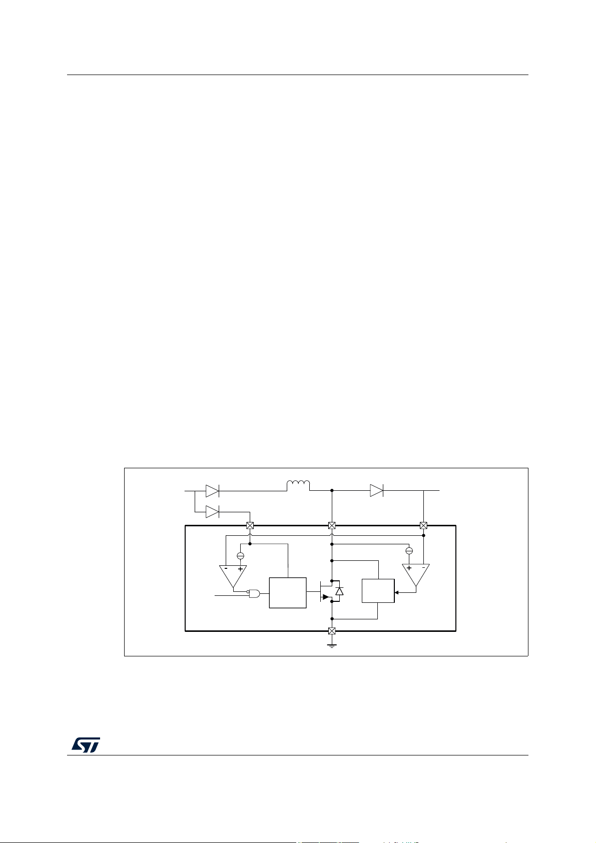
3.2 Boost regulator
The boost regulator can be enabled or disabled via SPI depending on the needs of the
application with respect to the operating battery level. It features an integrated power stage
and operates at 2
capability should be enough to grant full I/O pin supply and minimal µC operation.
When not used, BSTSW pin can be connected to ground and VBST directly to the protected
battery line. The device enables or keeps disabled the boost converter at start-up depending
on the external circuitry: if BSTSW pin is shorted to ground, the boost is disabled at power
up and kept disabled; in case the BSTSW experiences a high voltage at power up, given by
battery connection through the inductor, the boost is enabled. This condition is reported via
SPI with bit BOOST_KEPT_OFF of SUPPLY_CONTROL_2 register (it means that boost
has been kept off and will not operate).
Boost converter diagnostics include under voltage, reported via SPI and FAULT pin (if the
regulator is enabled). The integrated FET featuring the boost switch is protected against
short to battery by means of a thermal shutdown circuit. When thermal fault is detected the
FET is switched off and latched in this state until the related fault flag is read. In case of loss
of ground the FET is switched off and automatically reactivated as soon as ground
connection is restored. Over-voltage protection from load-dump and inductive flyback is
provided via an active clamp and a disable circuitry. A dedicated circuitry is implemented to
keep the boost off at start-up till the voltage difference between VB and VBST pins is lower
than BST_DISABLETH in order to reduce in-rush current and diagnose VBST pin loss
condition or diode loss. An SPI bit is present to report output of this comparator (bit
BOOST_READY of SUPPLY_CONTROL_2 register goes high when VBST>=VBBST_DISABLETH).
MHz to allow the use of external low cost 2.2 µH inductor. The current
State of boost regulator is reported via SPI bit BOOST_ON_FLAG in register
SUPPLY_CONTROL_2. In case boost is disabled due to diagnostic or battery voltage
above output regulation voltage this bit is cleared to 0.
Figure 3. Boost regulator block diagram
DS12539 Rev 3 19/109
108
Page 20

Power supply L9396
All electrical characteristics are valid for the following conditions unless otherwise noted:
-40 °C ≤ Tj ≤ +175 °C; 4.5 V ≤ VBATP ≤ 19 V
Symbol Parameter Conditions Min Typ Max Unit
VBST
NOV
VBST
UV_UP
VBST
UV_DN
Table 6. Boost regulator electrical characteristics
Design Info With
boost, VBST is more
Normal Operating
Voltage at VBST
VBST under voltage
release threshold
VBST under voltage
detection threshold
than minimum boost
output (> 6 V); Without
boost, VBST is
shorted to VBATP
VBST rising. VBST
under-voltage release
leads to charge pump
switch on
VBST falling. VBST
under-voltage
detection leads to
charge pump shut
down.
61319V
6.5 - 7.1 V
5.6 - 6 V
t
flt_VBST_UV
Under voltage filter
time
VBST Boost Output Voltage
I
O_BST
dV
dV
L
R
C
R
C
SR_ac
LR_ac
BST
LBST
BST
BST
BSTF
Boost Output
Current
Line Transient
Response
Load Transient
Response
Output Inductance
Output Inductance
Impedance
Output Bulk
Capacitance
Bulk Capacitor ESR Design Information - - 0.1 Ω
Output Filter
Capacitance
--12-µs
Across all line and
load (steady state)
Excluding current on
analog and digital 3.3V
All line, load;
dt = 100 µs
All line, load;
dt = 100 µs
8.55 - 9.6 V
20 - 300 mA
-8% - 8% %
-8% - 8% %
2.2 µH nominal
tolerance ±30%
1.6 - 2.8 µH
Design Information
Design Information - - 0.1 Ω
Design Information 1.76 - - µF
Min 100 nF nominal
Design Information
80 - - nF
Over Current
Detection
Switch R
DSon
- 1.2- 2A
---0.8Ω
R
I
OC
DSon
20/109 DS12539 Rev 3
Page 21

L9396 Power supply
Table 6. Boost regulator electrical characteristics (continued)
Symbol Parameter Conditions Min Typ Max Unit
V
BSTSW
BST_DISABLE
CLAMP_EN
f
BSTSW
t
BSTSW
T
JSDBST
T
HYS_TSDBST
I
BSTSW_LO_OFF
I
BSTSW_HI_OFF
BSTSW Voltage
Clamp
Active when not in
load dump
(VB
LOADDUMP
)
30 - 36 V
Voltage difference
between VB and
TH
VBST to deactivate
VB – VBST 1.6 - 2.6 V
the Boost regulator
Voltage difference
between BSTSW
TH
and VBST to activate
BSTSW – VBST 1.5 - 4.5 V
the Boost CLAMP
Operating Frequency - - f
BSTSW Transition
Time
VB = 4.5 V,
= 300 mA
I
O_BST
8 - 50 ns
/8.5(1.88) - MHz
OSCINT
Thermal Shutdown - 175 - 200 °C
Thermal Shutdown
hysteresis
-5-15°C
BSTSW current
consumption when
BSTSW - VBST<1.5V 3 - 20 µA
BOOST is OFF
BSTSW current
consumption when
BSTSW – VBST>4.5V 30 - 70 µA
BOOST is OFF
Voltage threshold to
V
TH_BST_KEEP_OFF
deactivate the Boost
regulator when not
used
3.3 Internal supply
The internal analog and digital part is supplied by the supply voltage VBST through
integrated voltage regulators. The generated voltage is monitored. In case of under/overvoltage, the device performs a power on reset (POR).
An undervoltage condition on VBST will lead to an internal reset of the IC. Above this
undervoltage threshold, full functionality is granted.
The device integrates two separated instances of Bandgap voltage regulators; one of these
bandgaps is used as voltage reference for the internal regulators, while the other one is
used for monitoring the voltage levels.
GNDD ground line is protected against ground loss scenarios. In case GNDD line would be
at least GNDD
GNDD is used for digital logic and charge pump while GNDA is used for analog blocks.
GNDBST is used for boost regulator only.
above the reference ground line GNDA, a POR is asserted.
OPEN
-0.5-1V
DS12539 Rev 3 21/109
108
Page 22

Power supply L9396
The device returns to normal operation with full functionality as soon as the POR is
released.
Symbol Parameter Conditions Min Typ Max Unit
Table 7. Internal supply electrical characteristics
GNDD
OPEN
T
FLT_ GNDD_OPEN
GNDBST
GNDBST
T
FLT_ GNDBST_OPEN
OPEN
PU
GNDD threshold GNDx = 0 180 300 420 mV
GNDD Open deglitch filter
time
--10-µs
GNDBST threshold GNDx=0 200 300 400 mV
GNDBST pull-up current Boost OFF 50 - 200 µA
GNDBST Open deglitch
filter time
-7.5-11µs
VDD VDD Output Voltage - 3.15 3.3 3.4 V
VDD
OV
VDD
UV
T
FLT_ VDD_OV_UV
VDD Over-voltage
threshold
VDD Under-voltage
threshold
VDD Over-voltage / Undervoltage deglitch filter time
-3.47-3.7V
- 2.7 - 2.9 V
--10-µs
VINTA VINTA Output Voltage - 3.2 3.3 3.4 V
VINTA
VINTA
OV
UV
VINTA Over-voltage
threshold
VINTA Under-voltage
threshold
-3.47-3.7V
- 2.95 - 3.13 V
VINTA Over-voltage /
T
FLT_ VINTA_OV_UV
Under-voltage deglitch filter
--10-µs
time
3.4 Wake-up input
The input pin IGN can be used as a wake up source connection. In case the voltage on IGN
pin raises above WAKE
The device moves to sleep in case IGN falls below WAKE
longer than WAKE
flt_down
transceiver inhibit outputs. A filter time is implemented to reject spurious glitches. The filter
time is started when the input signal exceeds the specified threshold.
All electrical characteristics are valid for the following conditions unless otherwise noted:
-40 °C ≤ Tj ≤ +175 °C; 4.5 V ≤ VBATP ≤ 19 V.
22/109 DS12539 Rev 3
for an interval longer than WAKE
high_th
. This input can be connected to ignition battery switches or
high_th
, the device wakes up.
flt_up
- WAKE
for an interval
hys
Page 23
L9396 Power supply
Charge Pump
CTANK
VBST VCP
GADG1801171544PS
C1 C2
VC1 VC2 VC3 VC4
Table 8. Wake-up input electrical characteristics
Symbol Parameter Conditions Min Typ Max Unit
VBATP = 19 V Wake
VB
stby_cur
Battery standby current
consumption
disable Sum of leakage
currents from BSTSW,
- - 30 µA
VBST, VB and VBM
WAKE
WAKE
WAKE
WAKE
WAKE
WAKE
high_th
low_th
hys
pd
flt_up
flt_down
Wake-up high voltage
threshold
Wake-up low voltage
threshold
Wake-up voltage
hysteresis
Wake-up pull down IGN = 14 V 300 - 900 kΩ
Wake up ON deglitch - - 10 - µs
Wake up OFF deglitch - - 10 - µs
-3.5--V
---1.5V
- 0.5 - 1.5 V
KA_period Keep-alive period - - 200 - ms
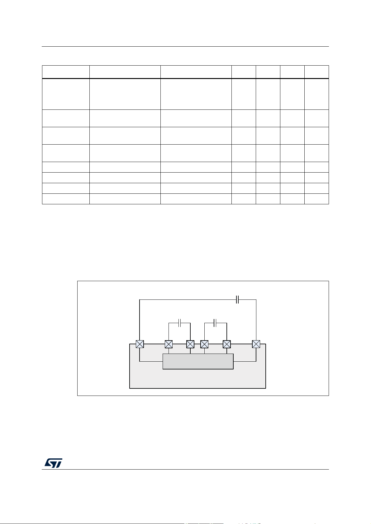
3.5 Charge pump
A two-stage charge pump is integrated to supply the high voltage circuit in the VPREREG
and VCORE regulators and in the pump motor and fail safe pre-drivers.
The charge pump is supplied by the rail connected to VBST pin. External charging
capacitors are used to achieve a high current capability.
Figure 4. Charge pump block diagram
It features a current limitation protection when either C1 or C2 is being charged up. The
charge pump is protected against over temperature with dedicated thermal sensor. In
standby mode the charge pump is disabled.
In case the CP output voltage remains too low for longer than tfCP the CP LOW bit is
latched, which leads to shutdown of VPREREG, pump motor driver and fail safe driver. In
turn, under voltage of VPREREG leads to shutdown of VCC, VCC5 and VCORE regulators.
DS12539 Rev 3 23/109
108
Page 24

Power supply L9396
A second undervoltage threshold is present (V
CPLOW2
) with a higher value. It can be used
together with PDG turn-on threshold voltage to detect that low charge pump voltage is
responsible for low PDG ON voltage.
Symbol Parameter Conditions Min Typ Max Unit
V
CP_5V6
V
CP_8V
V
CP_8V55
I
CP_5V6
I
CP_8V
f
CP
V
CPLOW
Charge pump
output voltage
Charge pump
output voltage
Charge pump
output voltage
Charge pump
output current
Charge pump
output current
Charge pump
frequency
Charge pump low
voltage threshold
Charge pump
V
CPLOW2
second low voltage
threshold
t
fCP
C
TAN K
, C
C
CP1
T
JSDCP
T
HYS_TSDCP
Low voltage filter
time
Output capacitor Design Info - 220 - nF
Switching capacitor Design Info - 68 - nF
CP2
Thermal Shutdown - 175 - 200 °C
Thermal Shutdown
hysteresis
Table 9. Charge pump electrical characteristics
VBST > 5.6 V
Iload_ext = 8 mA
VBST >8V
Iload_ext=10mA
VBST >8.55V
Iload_ext=1mA
VBST>5.6V - - 8 mA
VBST>8V - - 10 mA
--f
- VBST+5.6 VBST+6 VBST+6.8 V
- VBST+7.85 VBST+8.35 VBST+8.85 V
--10-µs
-5-15°C
VBST+7.0 - VBST+11 V
VBST+8.9 - VBST+11 V
VBST+9.1 - VBST+11 V
/34(0.470) - MHz
OSCINT
3.6 VPREREG buck regulator
The integrated buck regulator provides a reduced voltage supply to the remaining regulators
and to the WSS / tracking interface. Its default output level 6.5
7.2
V via register of BUCK VOLTAGE SELECTION in SPI.
This regulator is protected against short circuits and over temperature with dedicated
thermal sensor, and an over/under voltage monitor is implemented. VPREREG itself is not
shut down in case of over/under voltage at its output. VPREREG itself is not shut down in
case of overcurrent, only in case of over temperature the regulator is switched off.
This regulator is not protected against diode loss and the IC may be irreparably damaged
due to diode loss.
Under voltage of VPREREG (VPREREG_UV) leads to shutdown of VCC, VCC5 and
VCORE regulators.
24/109 DS12539 Rev 3
V can be further increased to
Page 25
L9396 Power supply
All electrical characteristics are valid for the following conditions unless otherwise noted:
-40 °C ≤ Tj ≤ +175 °C; 6 ≤ VBST ≤ 19 V.
Symbol Parameter Conditions Min Typ Max Unit
Table 10. VPREREG buck regulator
V
PREREG_H
V
PREREG_L
V
PREREG_UV
t
flt_VPREREG_UV
V
PREREG_OV
t
flt_VPREREG_OV
I
VPREREG_HI
I
VPREREG_LO
L
VPREREG
C
VPREREG
dV
SR_ac
dV
LR_ac
I
OC_VPREREG_HI
Output Voltage VBST > 8.2 V 6.984 7.2 7.416 V
Output Voltage VBST > 7.5 V 6.305 6.5 6.695 V
Under voltage
threshold
Under voltage
filter time
Over voltage
threshold
Over voltage
filter time
Output load
current
Output load
current
- 5.05 5.21 5.32 V
--12-µs
+5%
x
-
V
PREREG_
+10%
V
-
PREREG_
x
V
--12-µs
SYS_CONFIG_1[9]=1 0.01 - 1 A
SYS_CONFIG_1[9]=0
(default)
0.01 - 0.5 A
Buck inductor - 17.6 22 26.4 µH
Output
capacitor
Line Transient
Response
Load Transient
Response
- 14.3 22 29.7 µF
All line, load; dt = 10 µs
VBST> V
PREREG
(Typ)+3V
All line, load; dt = 10 µs
VBST> V
PREREG
(Typ)+3V
-8% - 8% %
-8% - 8% %
High Over
current
SYS_CONFIG_1[9]=1 1.8 - 3 A
detection
I
OC_VPREREG_LO
- High side t
- High side t
Fv
preregsw
R
DSon
t
softstart
Low Over
current
detection
on
off
Operating
Frequency
High side
Rds_ON
Softstart time
SYS_CONFIG_1[9]=0
(default)
0.9 - 1.6 A
---40ns
---40ns
f
/
--
OSCINT
34
-MHz
(0.470)
= 25 °C - - 0.4 Ω
T
j
T
= 175 °C - - 0.44 Ω
j
From 10% to 90% of
nominal output voltage
130 - 390 µs
DS12539 Rev 3 25/109
108
Page 26

Power supply L9396
Table 10. VPREREG buck regulator (continued)
Symbol Parameter Conditions Min Typ Max Unit
T
JSDVPRE
T
HYS_TSDVPRE
Thermal
Shutdown
Thermal
Shutdown
hysteresis
-175-200°C
-5-15°C
26/109 DS12539 Rev 3
Page 27
L9396 Power supply
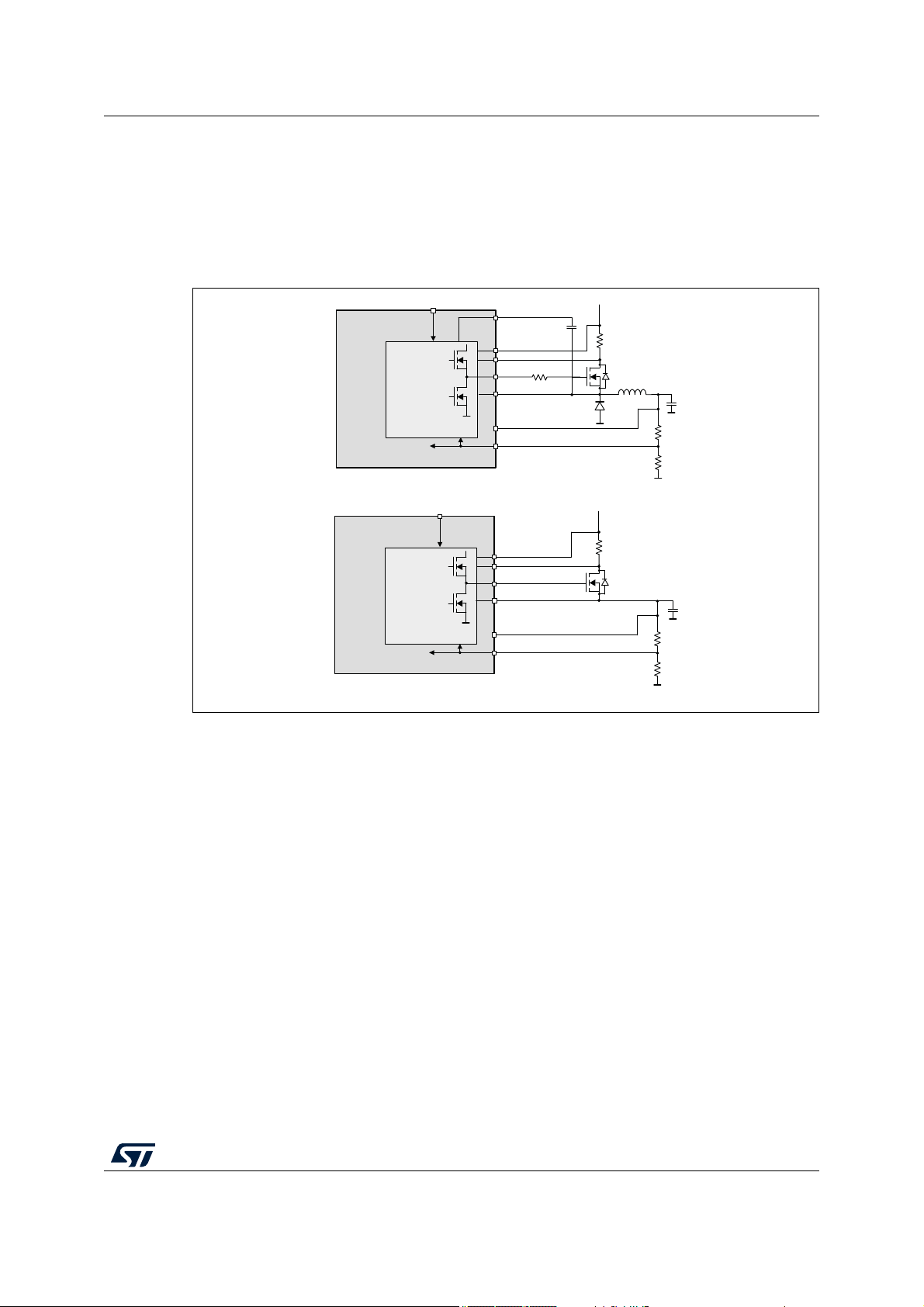
CP
Buck
Configuration
VCOREFDBK
GCORE
SCORE
VCORE
CBS
Linear
configuration
VCOREFDBK
GCORE
SCORE
VCORE
CP
GADG1901171138PS
I_CORE_SL
I_CORE_SH
I_CORE_SL
I_CORE_SH
(w/ Stop Mode bypass
with ext. FET
LDO)
Volt. Mon.
Volt. Mon.
22uH
VPREREG
VPREREG
L9396
L9396
3.7 VCORE regulator
This regulator provides the supply to the µC core. The flexible approach with the external
voltage divider allows the rail to be regulated from 0.8
either as a buck controller or as a linear controller, driving an external FET in both cases.
Figure 5. VCORE configuration diagram (buck regulator - top, linear regulator -
bottom)
V to 5 V. It can also be configured
Typically 100 Ω resistor is to be inserted between GCORE pin and gate of the external FET
for buck configuration. For buck configuration, the source of the external FET should be
connected to the SCORE pin, and the output tank capacitor should be connected to the
VCORE pin. For linear configuration, the output tank capacitor should be connected with the
source of the external FET and the SCORE pin, while VCORE pin could be left either
floating, tied to ground or still connected to VCORE to allow ADC internal measurement.
The VCORE regulator has over and under voltage detections and the VCORE is not shut
down in case of over or under voltage. It is also protected against short to ground by
monitoring regulation loop for VCORE buck or over current for VCORE linear. When short to
ground is detected and lasts more than the filter time of tflt_oc_vcore, the vcore is shut down
and the restart is automatic in tflt_restart. No thermal protection is implemented for VCORE
because the power MOS is external.
Both VPREREG and VCORE regulators could be disabled by connecting I_CORE_SH pin
to ground or leaving it open. In this case, VPREREG pin should be connected to VBST pin.
Moreover two pins (AI0 and AI1) are used to configure additional features of VCORE
regulator. It's possible to disable only VCORE regulator leaving VPREREG enabled. It's
possible to change the monitor of regulated voltage (monitor on VCORE pin or monitor on
VCOREFDBK pin). All the possibilities are listed in the following table.
DS12539 Rev 3 27/109
108
Page 28

Power supply L9396
Table 11. Vcore configuration
AI0 AI1 I_CORE_SH VCORE state VPREREG state VCORE monitor
Low Low High Enabled Enabled
Low High High Enabled Enabled
High Low High Enabled Enabled
VCORE_UV_L,
VCORE_OV_L
VCORE_UV_H,
VCORE_OV_H
VCOREFDBK_UV,
VCOREFDBK_OV
High High High Disabled Enabled Disabled
Don’t care Don’t care Low Disabled Disabled Disabled
The state of configuration pins (AI0, AI1 and I_CORE_SH) is latched at power up when
VPREREG voltage exceeds the V
PREREG_
UV threshold and stays latched until next POR
event.
Microcontroller can monitor the voltage of AI0 and AI1 pins using embedded ADC converter
and latched configuration is available via SPI bits.
All electrical characteristics are valid for the following conditions unless otherwise noted:
-40 °C ≤ Tj ≤ +175 °C; V
Table 12. VCORE regulator electrical characteristics
PREREG
_L(Min) ≤ VPREREG ≤ V
PREREG
_H(Max).
Symbol Parameter Conditions Min Typ Max Unit
R
SH_HI_CURR
R
SH_LO_CURR
VCORE FDBK_RES
VCOREFDBK_UV
VCOREFDBK_OV
Shunt resistor high
current
Shunt resistor low
current
Feedback resistor
range
Undervoltage
threshold
Overvoltage
threshold
- 99 100 101 mΩ
Only in linear mode 327 330 333 mΩ
- 10 - 100 kΩ
Excluding external
voltage divider
accuracy
Excluding external
voltage divider
accuracy
VCOREFDBK
– 10%
VCOREFDBK +
5%
VCOREFDBK
-
VCOREFDBK
-
– 5%
+ 10%
VCORE low
VCORE_UV_L
Undervoltage
- 2.97 - 3.135 V
threshold
VCORE low
VCORE_OV_L
Overvoltage
- 3.465 - 3.63 V
threshold
VCORE high
VCORE_UV_H
Undervoltage
- 4.5 - 4.75 V
threshold
V
V
28/109 DS12539 Rev 3
Page 29

L9396 Power supply
Table 12. VCORE regulator electrical characteristics (continued)
Symbol Parameter Conditions Min Typ Max Unit
VCORE high
VCORE_OV_H
t
flt_VCORE_VCOREFDBK
_UVOV
VICORESH_IH
Overvoltage
threshold
Under/overvoltage
filter time
I_CORE_SH input
high voltage
-5.25-5.5V
--12-µs
-1.75--V
VICORESH_IL
VICORESH_Ihys
Ipd_ICORESH_L
Ipd_ICORESH_B
V_AI0_IH
V_AI0_IL
I_CORE_SH input
low voltage
I_CORE_SH input
hysteresis
I_CORE_SH input
Pull down current
I_CORE_SH input
Pull down current
AI0 input high
voltage
AI0 input low
voltage
---0.75V
-100-1000mV
VCORE linear
mode,
5 - 20 µA
I_CORE_SH=3.3V
VCORE buck
mode,
100 - 300 µA
I_CORE_SH=3.3V
-1.75--V
---0.75V
V_AI0_Ihys AI0 input hysteresis - 100 - 1000 mV
Ipd_AI0
V_AI1_IH
V_AI1_IL
AI0 input Pull down
current
AI1 input high
voltage
AI1 input low
voltage
AI0=3.3V 10 - 100 µA
-1.75--V
---0.75V
V_AI1_Ihys AI1 input hysteresis - 100 - 1000 mV
Ipd_AI1
AI1 input Pull down
current
AI1 = 3.3 V 10 - 100 µA
From 10% to 90%
t
softstart
Softstart time
of nominal output
240 - 720 µs
voltage
Buck configuration
VCORE Output voltage
I
VCORE
C
VCORE
C
VCORE
Nominal 0.8V to 5V
Excluding external
voltage divider
0.776 - 5.15 V
accuracy
Output load current R
SH_HI_CURR
0.01 - 1 A
Output capacitor VCORE > 1.2 V -35% 22 +35% µF
Output capacitor VCORE ≤ 1.2V -35% 47 +35% µF
DS12539 Rev 3 29/109
108
Page 30

Power supply L9396
Table 12. VCORE regulator electrical characteristics (continued)
Symbol Parameter Conditions Min Typ Max Unit
L
VCORE
L
VCORE
R
LVC ORE
C
C
FET
BS
Buck inductor VCORE > 1.2 V -20% 22 +20% µH
Buck inductor VCORE ≤ 1.2 V -20% 12 +20% µH
Buck inductor
resistance
External FET gate
charge
- - - 105 mΩ
---30nC
Bootstrap capacitor - - 100 - nF
Excluding external
VCOREFDBK Feedback voltage
voltage divider
0.8 -3% - 0.8 +3% V
accuracy
dV
dV
SR_ac
LR_ac
Line Transient
Response
Load Transient
Response
All line, load;
dt = 10 µs
All line, load;
dt = 10 µs
-8% - 8% %
-8% - 8% %
VCORE ripple Ripple voltage - -20 - +20 mV
I
OC_VCORE_BUCK
Rdson_hs
Rdson_ls
Over current
detection
High side on
resistance
Low side on
resistance
R
SH_HI_CURR
---28Ω
---8.3Ω
1.6 - 2.6 A
tflt_oc_vcore
tflt_restart
Sw_fr
PSRR
Shut down filter
time for short to
ground
restart filter time for
short to ground
Switching
frequency
Power supply
rejection ratio
Filter time starts to
count from when
current in power
85 100 115 µs
MOS is more than
I
O_LIM
Filter time starts to
count from when
core buck is
1.7 2 2.3 ms
disabled
f
OSCINT
--
/34
-MHz
(0.470)
VPREREG = 6.5 V,
V
= 1 Vpp
noise
f
noise
C
VCORE
L
VCORE
= 20 kHz,
= 22 µF
= 22 µH
40 - - dB
30/109 DS12539 Rev 3
Page 31

L9396 Power supply
Table 12. VCORE regulator electrical characteristics (continued)
Symbol Parameter Conditions Min Typ Max Unit
Linear configuration
Nominal 0.8 V to
VCORE Output voltage
5 V Excluding
external voltage
divider accuracy
0.78 - 5.125 V
I
VCORE_HI
I
VCORE_LO
C
VCORE
R
CVCORE
C
VCORE_EMI
C
FET
Output load current
high
Output load current
low
R
SH_HI_CURR
R
SH_LO_CURR
Output capacitor - 5 - 40 µF
Output capacitor
ESR
Drain output
stability capacitor
External FET gate
charge
-0.01-0.1Ω
-0.1--µF
---50nC
0.07 - 0.75 A
0.07 - 0.25 A
Excluding external
VCOREFDBK Feedback voltage
voltage divider
0.8 -2.5% - 0.8 + 2.5% V
accuracy
dV
SR_ac
dV
LR_ac
GCORE_pd
Line Transient
Response
Load Transient
Response
Gate internal pull
down
All line, load;
dt = 10 µs
All line, load;
dt = 10 µs
Not tested,
guaranteed by
design.
-5% - 5% %
-5% - 5% %
100 - - kΩ
GCORE_Vclamp Gate voltage clamp - 8 - 12 V
I
COREL_HI
I
COREL_HI
Ilim
_OC
High Current
limitation
High Overcurrent
threshold
-0.8-1.6A
-0.8-1.6A
I
COREL_LO
I
COREL_LO
tflt_oc_vcore
Ilim
_OC
Low Current
limitation
Low Overcurrent
threshold
Shut down filter
time for short to
ground
- 0.26 - 0.48 A
- 0.26 - 0.48 A
Filter time starts to
count from when
current in power
85 100 115 µs
MOS is more than
Ilimx
I
COREL
DS12539 Rev 3 31/109
108
Page 32

Power supply L9396
Table 12. VCORE regulator electrical characteristics (continued)
Symbol Parameter Conditions Min Typ Max Unit
Filter time starts to
tflt_restart
restart filter time for
short to ground
count from when
core buck is
1.7 2 2.3 ms
disabled
VPREREG = 6.5V,
= 1 Vpp
V
PSRR
Power supply
rejection ratio
noise
f
= 20 kHz,
noise
C
VCORE
L
VCORE
40 - - dB
= 22µF
= 22µH
3.8 VCC5 regulator
This regulator provides a fixed 5V rail to supply µC I/Os and ADC. The VCC5 regulator has
over and under voltage detections and is also protected against short circuits and over
temperature with shared thermal sensor with VCC regulator.
All electrical characteristics are valid for the following conditions unless otherwise noted:
-40 °C ≤ Tj ≤ +175 °C; V
Table 13. VCC5 regulator electrical characteristics
PREREG
_L(Min) ≤ VPREREG ≤ V
PREREG
_H(Max).
Symbol Parameter Conditions Min Typ Max Unit
VCC5
VCC5_UV
Regulated output
voltage
Undervoltage threshold -
VCC5_OV Overvoltage threshold -
t
flt_VCC5_UVOV
I
VCC5
C
VCC5
C
ESR Output capacitor ESR - 0.01 - 0.1 Ω
VCC5
dV
SR_ac
dV
LR_ac
R
DSon
Under/overvoltage filter
time
Output load current - 0 - 250 mA
Output capacitor - 2.2 4.7 20 µF
Line Transient
Response
Load Transient
Response
High side Rds_ON - - - 4 Ω
0mA ≤ I
250mA
--12-µs
All line, load;
dt = 10 µs
All line, load;
dt = 10 µs
VCC5
≤
4.88 5 5.12 V
VCC5 -
10%
VCC5 +
5%
-
-
VCC5 -
5%
VCC5 +
10%
-5% - 5% %
-5% - 5% %
VCC5_cur lim Current limitation - 300 - 600 mA
VCC5_oc Overcurrent threshold - 300 - 600 mA
VCC5_ilim_oc_delta Delta_Ilim_Oc
VCC5_cur_lim –
VCC5_oc
0.1 - 100 mA
V
V
32/109 DS12539 Rev 3
Page 33

L9396 Power supply
Table 13. VCC5 regulator electrical characteristics (continued)
Symbol Parameter Conditions Min Typ Max Unit
From 10% to 90%
t
softstart
Softstart time
of nominal output
345 - 1035 µs
voltage
T
JSDVCCx
T
HYS_TSDVCCx
Thermal Shutdown - 175 - 200 °C
Thermal Shutdown
hysteresis
-5-15°C
3.9 VCC regulator
This regulator provides a dedicated rail to supply µC I/Os. It can be configured via VCCSEL
pin to output either 3.3 V or 5 V. The VCC regulator has over and under voltage detections
and is also protected against short to ground and over temperature with shared thermal
sensor with VCC5.
The state of VCCSEL pin is latched at power up when VPREREG voltage exceeds the
VPREREG_UV threshold and stays latched until next POR event.
All electrical characteristics are valid for the following conditions unless otherwise noted:
-40 °C ≤ Tj ≤ +175 °C; V
Table 14. VCC regulator electrical characteristics
PREREG
_L(Min) ≤ VPREREG ≤ V
PREREG
_H(Max).
Symbol Parameter Conditions Min Typ Max Unit
VCC_L
VCC_H
VCCSEL_IH
VCCSEL_IL
VCCSEL_Ihys
Ipd_VCCSEL
VCC_UV
Regulated output
voltage
Regulated output
voltage
VCCSEL input high
voltage
VCCSEL input low
voltage
VCCSEL input
hysteresis
VCCSEL input Pull
down current
Undervoltage
threshold
VCC_OV Overvoltage threshold -
t
flt_VCC_UVOV
Under/overvoltage
filter time
0mA ≤ I
VCCSEL = ‘0’
VPREREG ≥ 6V, 0mA
≤ I
VCC
VCCSEL = ‘1’
-1.75--V
---0.75V
- 100 - 1000 mV
VCCSEL=3.3V 1 - 10 µA
-
--12-µs
≤ 100mA;
VCC
≤ 100mA;
3.220 3.3 3.380 V
4.88 5 5.12 V
VCC_x
- 10%
VCC_x
+ 5%
-
-
VCC_x -
5%
VCC_x +
10%
V
V
I
C
VCC
VCC
Output load current - 0 - 100 mA
Output capacitor - 2.2 4.7 20 µF
DS12539 Rev 3 33/109
108
Page 34

Power supply L9396
Table 14. VCC regulator electrical characteristics (continued)
Symbol Parameter Conditions Min Typ Max Unit
C
ESR Output capacitor ESR - 0.01 - 0.1 Ω
VCC
dV
SR_ac
dV
LR_ac
R
DSon
VCC_cur lim Current limitation - 125 - 240 mA
VCC_oc Overcurrent threshold - 125 - 240 mA
VCC_ilim_oc_delta Delta_Ilim_Oc
t
softstart
Line transient
response
Load transient
response
High side Rds_ON - - - 12 Ω
Softstart time
All line, load;
dt = 10 µs
All line, load;
dt = 10 µs
VCC_cur_lim –
VCC_oc
From 10% to 90% of
nominal output
voltage
-5% - 5% %
-5% - 5% %
0.1 - 100 mA
345 - 1035 µs
3.10 Protected battery switch
The device provides a fully protected switched battery output VB_SW, always active when
the device is not in stand-by mode and WD1 is correctly served. This functionality can be
used as further battery supply, e.g. for external sensors requiring battery level, or as a pullup voltage rail.
The output can be disabled through SPI. Should the VB_SW diagnostics detect an over
current condition, the output is turned off and the over current SPI fault is set. Once an overcurrent condition is detected, the output can only be re-enabled through SPI command,
when the fault disappears, writing the bit PROTECTED BATTERY SWITCH COMMAND at
1 after the related OVER CURRENT flag is cleared on read.
All electrical characteristics are valid for the following conditions unless otherwise noted:
-40 °C ≤ Tj ≤ +175 °C; 4.5 ≤ VB = VBATP ≤ 19 V.
Symbol Parameter Conditions Min Typ Max Units
- Saturation voltage
- Operating current - - - 150 mA
VB_SW_oc
VB_SW _cur lim Current limitation - 165 - 250 mA
VB_SW _ilim_oc_delta Delta_Ilim_Oc
Table 15. Protected battery switch electrical characteristics
Overcurrent
shutdown
VB – VB_SW @
max. current
-165-250mA
VB_SW_cur_lim –
VB_SW_oc
--0.5V
0.1 - 20 mA
34/109 DS12539 Rev 3
Page 35

L9396 Power supply
VBATP
IGN
ON
VPREREG
VCORE
VPREREG _UV
RESET
OFF
Ton
RESET
VCC
GADG1901171330PS
VCC5_UV
VCORE_UV
VCC_UV
VCC_dly
VCC5_dly
WAKE_FLT_up
St-by
VCC 5
Table 15. Protected battery switch electrical characteristics (continued)
Symbol Parameter Conditions Min Typ Max Units
-
Ileak
Shutdown delay
time
Off state leakage
current
-90-110µs
VB_SW off -1 - 1 µA
3.11 Power up and power down sequences
Wake-up signal turns on the device and initiates the regulator power up sequence as in the
figure below.
Figure 6. Power up sequence from wake up input
The device provides three different possibilities to stay in ON state:
a persistent high signal on IGN pin,
the setting of the POWERHOLD bit through SPI,
the refreshing of the KEEPALIVE bit through SPI within a specified time frame.
At each transition H->L on the wake-up pin the device enters the keep-alive mode for one
keep-alive period (KA_period).
DS12539 Rev 3 35/109
108
Page 36

Power supply L9396
VBATP
13.5V
VCC5_UV
VCC_UV
VPREREG
IGN
VCC5
VCC
RESET
WAKE_FLT_down
KA_period
VCORE
Tflt_VCC5_UVOV/Tflt_VCC_UVOV/Tflt_VCORE_VCOREFDBK_UVOV
VCORE_dly
VDD_UV/VINTA_UV
VDD/VINTA
POR
Tflt_ VDD_OV_UV / Tflt_ VINTA_OV_UV
GADG1901171502PS
If the device receives an SPI command to set the POWERHOLD bit within the first keepalive period the device remains awake. Similarly, if the device receives an SPI command to
refresh the KEEPALIVE bit within the first keep-alive period the device remains awake.
Once the KEEPALIVE bit is refreshed a new KA_period starts and so forth. To stay on the
keep-alive bit should be refreshed at each KA_period.
Should the KA_period elapse without any of the above 3 conditions, the device exits the
keep-alive mode and enters in power down.
The power down sequence depends on the keep alive choice being done.
In the following figure, the power down sequence related to a H->L transition on the wake-
up input pin without SPI conditioning is shown.
Figure 7. Power down sequence from wake up input
Table 16. Power up and power down
Symbol Parameter Conditions Min Typ Max Units
VCC5_dly
VCC_dly
VCORE_dly
VCC5 delay at
power-up
VCC delay at
power-up
VCORE delay at
power-down
Ton_RESET RESET hold time
From VPREREG_UV to VCC5
start
From VPREREG_UV to VCC
start
From end of KA_period
VCORE switch off
From regulators in range to
RESET High
to
-200 - µs
-200 - µs
-200 - µs
11 12 13 ms
36/109 DS12539 Rev 3
Page 37

L9396 Pre-drivers
4 Pre-drivers
4.1 Fail safe pre-driver
The device integrates a pre-driver of an external FET for fail safe purposes. It can be used
as a HS pre-driver in case the external FET is used as a switch. The device controls the fail
safe pre-driver in On/Off via SPI. The function remains active while no internal voltage faults
or watchdog faults are detected.
This pre-driver implements a monitor against over current thanks to the diagnostics on
drain-source monitoring of the external FET (in case of overcurrent SPI bit 15 of
DRV_CONTROL_1 register goes high). If charge pump level goes below the disable
voltage, the pre-driver is turned off. When the level returns above the disable voltage, the
pre-driver returns to normal operation.
Symbol Parameter Conditions Min Typ Max Units
VDG_ON VDG On voltage (VDG-VDS)@-0.1mA 5.2 - 12 V
VDG_OFF VDG Off voltage (VDG-VDS)@0.1 mA - - 1 V
Rpd_VDG_VDS
VDG_Isource VDG current source
Table 17. Fail Safe pre-driver electrical characteristics
Pull down resistor at VDGVDS
-130-270kΩ
V(VDG)=V(VDS)
V(CP)– V(VDG)=2V
0.2 1 2 mA
VDG_Isink VDG current sink V(VDG)-V(VDS)=1V 1 5 9 mA
QFS_turn-on_00
QFS_turn-on_01
QFS_turn-on_10
QFS_turn-on_11
IVDBATT_ds
t
QFS_ON
QFS turn-on threshold
voltage
QFS turn-on threshold
voltage
QFS turn-on threshold
voltage
QFS turn-on threshold
voltage
VDBATT leakage current
for drain-source monitor
Filter time of QFS turn-on guaranteed by scan - 12 - µs
V(VDBATT) – V(VDS)
VDS_TH=’00’
V(VDBATT) – V(VDS)
VDS_TH=’01’
V(VDBATT) – V(VDS)
VDS_TH=’10’
V(VDBATT) – V(VDS)
VDS_TH=’11’
FAIL SAFE DRIVER
ENABLE=0
0.25 - 0.75 V
0.75 - 1.25 V
1.25 - 1.8 V
1.75 - 2.4 V
7 - 67 µA
DS12539 Rev 3 37/109
108
Page 38

Pre-drivers L9396
4.2 Pump motor pre-driver
The device can drive a pump motor through this pre-driver for external FETs. It provides predriver circuitry for the motor high-side FET and the motor recirculation FET.
The PDG gate drive signal is referenced to PDS, and the pre-driver pair shall be able to float
below the logic ground voltage, while keeping full on/off control on the external FET. This is
required to prevent the FET from being partially turned on in the case of a ground offset
between ECU and motor ground, or in case of loss of ECU ground.
Similarly, the PRG gate drive signal shall be referenced to PRS, and the pre-driver pair shall
be able to float below the logic ground voltage, while keeping full on/off control on the
external recirculation FET.
The motor FET pre-drivers shall be controlled by logic level input pins PDI and PRI, with
logical operation defined as:
PDI PRI PDG PRG High-side FET Recirculation FET
L L L L OFF OFF
H L H L ON OFF
L H L H OFF ON
H H H L ON OFF
Table 18. Logical operation definition
The state of the PDI and PRI pins can be observed via SPI.
The device is able to generate software selectable dead time between PDG and PRG
transitions, to prevent cross-conduction on the external FETs.
In order to enable either PDG or PRG the following conditions must be met:
the watchdog reset must not be asserted,
the Enable Motor FET Driver SPI bit must be set,
no device faults preventing PDG or PRG operation must be present.
When disabled, PDG and PRG are driven to their low states.
4.3 Pump motor diagnostics
To enable MCU diagnostics, the device provides an internal pull-up current (IPDS) on PDS
and the PDS voltage can be read by the ADC and available over SPI.
After PDG is turned on, the device monitors the rising differential voltage between PDG and
PDS. If the differential voltage does not exceed the PDG turn-on voltage threshold within the
PDG switching time, the device disables the PDG pre-driver and sets the PDG Turn-On
Fault SPI bit. The device automatically re-enables the PDG pre-driver on the next rising PDI
edge.
After PDG is turned off, the device monitors the falling differential voltage between PDG and
PDS. If the differential voltage does not drop below the PDG turn-off voltage threshold within
the PDG switching time, the device disables both the PDG and PRG pre-drivers, sets the
PDG Turn-Off Fault SPI bit and clears the Enable Motor FET Driver SPI bit. The PDG and
38/109 DS12539 Rev 3
Page 39

L9396 Pre-drivers
PRG pre-drivers remain disabled until the Enable Motor FET Driver SPI bit is re-set over
SPI. The PDG Turn-On/off Fault SPI bits are latched until read.
In case the negative flyback voltage on PDS drops below the open flyback voltage threshold
for longer than the open flyback debounce time after PDG is turned off, the device disables
both the PDG and PRG pre-drivers, sets the Open Flyback Fault SPI bit and clears the
Enable Motor FET Driver SPI bit. The PDG and PRG pre-drivers remain disabled until the
Enable Motor FET Driver SPI bit is re-set over SPI. The Open Flyback Fault SPI bit is
latched until read.
After PDG is turned on, the device monitors the falling differential voltage between PDBATT
and PDS. If the differential voltage does not drop below the QPD turn-on voltage threshold
within the QPD switching time, the device disables the PDG pre-driver and sets the QPD
Turn-On Fault SPI bit. The device automatically re-enables the PDG pre-driver on the next
rising PDI edge. The QPD Turn-On Fault SPI bit is latched until read.
After PDG is turned off, the device monitors the falling PDS voltage. If the voltage does not
drop below the QPD turn-off voltage threshold within the QPD switching time, the device
disables both the PDG and PRG pre-drivers, sets the QPD Turn-Off Fault SPI bit and clears
the Enable Motor FET Driver SPI bit. The PDG and PRG pre-drivers remain disabled until
the Enable Motor FET Driver SPI bit is re-set over SPI. The QPD Turn-Off Fault SPI bit is
latched until read.
After PRG is turned on, the device monitors the rising differential voltage between PRG and
PRS. If the differential voltage does not exceed the PRG turn-on voltage threshold within the
PRG switching time, the device sets the PRG Turn-On Fault SPI bit. The device continues
to drive the current limited PRG pin. The PRG Turn-On Fault SPI bit is latched until read.
After PRG is turned off, the device monitors the falling differential voltage between PRG and
PRS. If the differential voltage does not drop below the PRG turn-off voltage threshold within
the PRG switching time, the device disables both the PDG and PRG pre-drivers, sets the
PRG Turn-Off Fault SPI bit and clears the Enable Motor FET Driver SPI bit. The PDG and
PRG pre-drivers remain disabled until the Enable Motor FET Driver SPI bit is re-set over
SPI. The PRG Turn-On Fault SPI bit is latched until read.
All the OFF diagnostic comparators (PDG_OFF, open flyback, QPD_OFF, PRG_OFF) are
active during the entire OFF state until FETs are switched on. Output of comparators is
masked when Enable Motor FET Driver SPI bit is low while is not masked when Enable bit
is high and FETs are in off state. There is no masking of OFF diagnostic when there is
transition of Enable Motor FET Driver SPI bit from low to high. Masking time is only applied
during the transitions of FETs gate command.
In case of a device ground loss while the motor is enabled, the device disables both external
FETs. These FETs remain disabled until the device returns to the active mode.
If battery level goes below the disable voltage, the pre-driver is turned off after the delay
disable time has elapsed. When the level returns above the disable voltage, the pre-driver
returns to normal operation.
DS12539 Rev 3 39/109
108
Page 40

Pre-drivers L9396
Table 19. Pump motor diagnostics electrical characteristics
Symbol Parameter Conditions Min Typ Max Units
PDG_ON_5V6
PDG_ON_8V
PDG_ON_8V55
PDG_OFF
-
-
Rpd_PDG_PDS
-
-
QPD_turn-on_00
QPD_turn-on_01
QPD_turn-on_10
QPD_turn-on_11
IPDBATT_ds
QPD_turn-off_th
-
PDG On
voltage
PDG On
voltage
PDG On
voltage
PDG Off
voltage
PDG turn-on
threshold
voltage
PDG turn-off
threshold
voltage
Pull down
resistor at
PDG-PDS
PDG switching
time
PDG filter
time
QPD turn-on
threshold
voltage
QPD turn-on
threshold
voltage
QPD turn-on
threshold
voltage
QPD turn-on
threshold
voltage
PDBATT
leakage current
for drain-source
monitor
QPD turn-off
threshold
voltage
QPD switching
time
(V(PDG)-V(PDS))@1mA@VBST>5.6V
assuming PDBATT=VBST
(V(PDG)-V(PDS))@10mA@VBST>8V
assuming PDBATT=VBST
(V(PDG)-V(PDS))@1mA@VBST>8.55V
assuming PDBATT=VBST
(V(PDG)-V(PDS))@1mA - - 0.5 V
V(PDG) – V(PDS) 5.1 6 6.8 V
V(PDG) – V(PDS) 0.5 - 1 V
-130-270kΩ
guaranteed by scan - 6 - µs
guaranteed by scan - 3 - µs
V(PDBATT) – V(PDS)
PUMP_VDS_TH=’00’
V(PDBATT) – V(PDS)
PUMP_VDS_TH=’01’
V(PDBATT) – V(PDS)
PUMP_VDS_TH=’10’
V(PDBATT) – V(PDS)
PUMP_VDS_TH=’11’
PUMP MOTOR PRE
DRIVER ENABLE=0
V(PDBATT) – V(PDS) -
guaranteed by scan - 6 - µs
6.8 - 12 V
7.8 - 12 V
8.9 - 12 V
0.25 - 0.75 V
0.75 - 1.25 V
1.25 - 1.8 V
1.75 - 2.4 V
7 - 67 µA
QPD_turn-
on_th
-V
40/109 DS12539 Rev 3
Page 41

L9396 Pre-drivers
Table 19. Pump motor diagnostics electrical characteristics (continued)
Symbol Parameter Conditions Min Typ Max Units
- QPD filter time guaranteed by scan - 3 - µs
-
-
PDG_Isource
PDG_Isink
PRG_ON
PRG_OFF
-
-
Rpd_PRG_PRS
-
Open flyback
threshold
Open flyback
filter time
PDG current
source
PDG current
sink
PRG On
voltage
PRG Off
voltage
PRG turn-on
threshold
voltage
PRG turn-off
threshold
voltage
Pull down
resistor at
PRG-PRS
PRG switching
time
--11--7.5V
--3-µs
V(PDG)=V(PDS)
V(CP)-V(PDG) = 2 V
15 25 35 mA
V(PDG) – V(PDS) = 1 V 15 25 35 mA
(V(PRG)-V(PRS))@1 mA@VBST>5.6 V
6.8 - 12 V
(V(PRG)-V(PRS))@1 mA - - 0.5 V
V(PRG)-V(PRS) 5.1 - 6.8 V
V(PRG)-V(PRS) 0.5 - 1 V
-130-270kΩ
guaranteed by scan - 6 - µs
- PRG filter time guaranteed by scan - 3 - µs
PRG_Isource
PRG_Isink
-
-
PDI _IH
PDI _IL
PDI _Ihys
Ipd_PDI
PRG current
source
PRG current
sink
PDI
propagation
delay
PRI
propagation
delay
PDI input high
voltage
PDI input low
voltage
PDI input
hysteresis
PDI input Pull
down current
V(PRG)=V(PRS)
V(CP)-V(PRG)=2V
15 25 35 mA
V(PRG) – V(PRS)=1V 15 25 35 mA
From PDI rising edge to
PDG at turn-on threshold
-2-µs
voltage
From PRI rising edge to
PRG at turn-on threshold
-2-µs
voltage
-1.75--V
---0.75V
- 100 - 1000 mV
PDI=3.3V 10 - 100 µA
DS12539 Rev 3 41/109
108
Page 42

Pre-drivers L9396
Table 19. Pump motor diagnostics electrical characteristics (continued)
Symbol Parameter Conditions Min Typ Max Units
PRI _IH
PRI _IL
PRI _Ihys
Ri_pd_PRI
-
PRI input high
voltage
PRI input low
voltage
PRI input
hysteresis
PRI input Pull
down current
Non overlap
timing
-1.75--V
---0.75V
- 100 - 1000 mV
PRI=3.3V 10 - 100 µA
Programmable in 24 steps - 0.25 6 µs
42/109 DS12539 Rev 3
Page 43

L9396 Remote sensor interface
5 Remote sensor interface
The device contains 4 remote sensor interfaces, capable of supporting active wheel speed
sensors or operating as an independent 2-channel tracking regulation supply.
The interface supply is internally connected to the VPREREG pin. The circuitry consists of a
power interface delivering a dedicated output voltage on RSUHx pins. This output could be
voltage regulated in case of operation as tracking supply (pins RSUH0 and RSUH1). When
WSS operation is selected, the function mirrors the current flowing in the external sensor
and transmits this current information to the decoder, which produces a digital value for
each sensor channel. RSULx pins are used as ground returns from the sensors and current
sense is carried out in low side.
Data are then output through SPI registers. Received signals can be processed to the
corresponding discrete logic output pin WSO0-WSO3.
5.1 Active wheel speed sensor
The remote sensor interface circuit conditions and interprets active wheel speed sensor
signals with various pulse widths and output currents. The following sensor types are
supported and selected through SPI configuration:
Standard active 2-level wheel speed sensors (7/14 mA);
A three-level (7/14/28 mA) VDA compliant sensor with direction and air gap information
("Requirement Specification for Standardized Interface for Wheel Speed Sensor with
Additional Information", Version 4.0);
PWM encoded 2-level sensors with 2 edges per tooth (see data sheet Infineon IC
TLE4942/BOSCH DF11);
PWM encoded 2-level sensors with 1 edge per tooth (see data sheet Allegro
ATS651LSH/BOSCH DF11).
Received wheel speed frames from all the above sensors are decoded into signals suitable
for the microcontroller through SPI or the four WSOx output pins. For all sensors, other than
the standard active 2- level sensor, additional sensor data (diagnostics, etc…) are decoded
and available within SPI registers. The user may select to have all sensor data processed
on WSOx pins through the microcontroller by selecting pass through mode. In pass through
mode, the remote sensor interface simply conditions the incoming sensor current pulses to
digital pulses, no decoding is performed.
The sensor input filter time, deglitch filter, (delay until a threshold crossing is detected) can
be configured (from 8 µs to 50 µs). Filters can be selected individually for each channel,
through the RS_CFG_x_y registers, bits [9:6].
For PWM encoded sensors with 2 edges per tooth not in pass through mode, the standstill
signal can be processed directly to the WSOx output pins. This is done in the RS_CFG_x_y
registers, bit [4].
Since the decoder has to measure the pulses in order to determine whether they are standstill pulses or not, the first standstill pulse will always be seen on the WSOx output pins and
the first not stand-still pulse after a stand-still period will be suppressed.
DS12539 Rev 3 43/109
108
Page 44

Remote sensor interface L9396
GADG1901171624PS
Sensor current
WSO pin
Bit SSDIS = 1
First not stand still
pulse is suppressed
WSO pin
Bit SSDIS = 0
Stand still time
Figure 8. Standstill operation diagram
Data from the sensor are not latched: last incoming frame overwrites the previous one once
validated. Faults coming from diagnostic (i.e. over current, short to ground or battery) are
latched until the microcontroller reads them.
We have two different digital algorithms:
Auto-adjusting current trip points. With this option, the IC is able to find sensor base
current value (named IB0). Range of base current can be configured via SPI. The IC is
also able to detect the current value of the data pulse and compute the first threshold
(named Ith1): Ith1 = IB0 + (ΔIth1)/2 where ΔIth1 range is also configurable via SPI.
Besides, in case of VDA selected, the IC is also able to recognize the current value of
the speed pulse by computing a second threshold (named Ith2): Ith2 = IB0 + ΔIth1 +
(ΔIth2)/2 where ΔIth2 range is configurable via SPI.
Fixed current trip points where the thresholds are set by SPI. To avoid the risk of wrong
settings (inverted thresholds, thresholds outside WSI limits and similar) only the first
threshold can be directly programmed while, to determine the second one, an offset vs.
the first threshold must be provided. Both values, threshold and offset, can be specified
through an 8-bit word (range 0x00 → 0xFF). A fixed offset of 54 (0x36) is also added to
determine the actual thresholds in order to prevent any potential wrong setting out or
range. Complete formulas for threshold computation are the following:
– First threshold (typ.) = 93.75 µA*(54 +WSI_FIRST_TH)
– Second threshold rising edge (typ.) =
93.75 µA*(108+WSI_FIRST_TH+WSI_OFFS_TH)
– Second threshold falling edge (typ.) =
93.75 µA*(108+WSI_FIRST_TH+WSI_OFFS_TH)*0.6865
– WSI_FIRST_TH: SPI programmable from 0x00 to 0xFF (default = 0x33)
– WSI_OFFS_TH: SPI programmable from 0x00 to 0xFF (default = 0x34)
44/109 DS12539 Rev 3
Page 45

L9396 Remote sensor interface
GADG2001170743PS
Three levels current
(VDA compliant sensor
with Manchester encoded
information)
Three levels current
(Standard compliant sensor
with only speed information
information)
Two levels current PWM
(One pulse per tooth with data
encoded in pulse width)
Two levels current PWM
(Two pulses per tooth with data
and diagnostic encoded
in pulse width)
WSx pin
WSx pin
WSx pin
Data and diagnostic by SPI: Three level sensors have eight data bits and a parity bit which are written into the register upon
receiving At higher speeds not all bits can be transmitted. The data register for each wheel contains the number of data bits
received between two speed pulses.
Data by WSx pin (Pass-through model)
Data by WSx pin and Duty cycle info by SPI
(Normal mode)
WSx pin
Data by WSx pin and Duty cycle info by SPI
(Normal mode)
(Pass-through model)
(Pass-through model)
high
db0
I
THopen
I
TH1
I
TH2
db1 db2 db3 db4 db5 db6 db7 p
high highlow highhighhighhighlow
28mA
I
TH1
14mA
7mA
45μs
45μs n x 45μs
45μs 90μs 90μs
I
TH1
14mA
7mA
I
TH1
14mA
7mA
7mA
Figure 9. Wheel speed sensor protocol types
DS12539 Rev 3 45/109
108
Page 46

Remote sensor interface L9396
5.1.1 Wheel speed data register formats
In the wheel speed sensor interface four data registers are used (Remote Sensor Data
Register RS_DATA_RSDR_0- RS_DATA_RSDR_3).
Independent data registers are defined for each wheel speed channel and their contents are
determined by sensor type. Three-level VDA sensors have eight data bits and parity as
shown in the table below. At fast speed not all bits may be transmitted by the sensor: the IC
is able both to process normal or either truncated frames by providing together with data, a
4-bit counter to inform the microcontroller about the number of received valid bits.
For PWM encoded sensors, each pulse length is written to the sensor data register with a
typical resolution of 5 µs per bit. In case of pulse width duration equal to or higher than
1.045
ms, the standstill condition will be recognized and bit 15 in the corresponding register
will be set.
The register is updated when a PWM falling edge is detected; in case of stuck-at 1 of the
PWM signal the register is updated when the counter reaches the overflow value (0x1FF): in
this case the standstill bit not set and the counter in overflow will signal a fault to the
microcontroller.
5.1.2 Testmode
In order to test the input structures of the connected microcontroller, the device features a
wheel speed test mode that allows test patterns to be applied on the four wheel speed
outputs WSOx. The test mode can be entered via SPI and the test patterns can also be
controlled via SPI commands. Test patterns can be composed only of static high or low
signals, which can be selected via SPI. For safety reasons only one channel at a time can
be switched into test mode.
In order to enable testmode it is necessary to write to '1' bit DIAG (bit 4) of register
RS_CTRL. After that the bits of WSS_TEST register select the channel under test and the
state of output pin.
To exit this testmode it is not sufficient to clear to '0' the DIAG bit but, before that, also bits
8:2 of WSS_TEST register (Config range field) must be changed in order not to select any of
the four available outputs.
5.1.3 Wheel Speed SPI Registers
WSI test
Addr Name Type Bits = 9
0001111 WSS_TEST RW Config Range= 8:2, X:1, TestBit = 0;
WSS_TEST register stores Static Test configurator bit-field.
This register configures a static test for WSI interface. Test consists in transferring TestBit
value on a selected (by Config range) WSI output.
TestBit: Test input value.
Table 20. WSS_TEST register
46/109 DS12539 Rev 3
Page 47

L9396 Remote sensor interface
Table 21. WSS_TEST register bit description
Data Field Description Reset value Reset Event
Config range: selects one WSI
output according to the following
range:
Bit 8:2
1010011 => DOUT4 output;
1010101 => DOUT3 output;
0
SSM_RESET
LBIST
1011001 => DOUT2 output;
1010110 => DOUT1 output;
all others: test mode disabled
Bit 1 DON’T CARE 0
SSM_RESET
LBIST
WSSTP: DOUTx Output Test Value
Bit 0
0 => Output for selected DOUTx
set ‘high’
1 => Output for selected DOUTx
0
SSM_RESET
LBIST
set ‘low’
WSI configuration
Table 22. RS_CFG_0_1 register
ADDR Name Type Bits = 20
0001100 RS_CFG_0_1 RW Config1 Range ch1 = 19:10, Config0 Range ch0 = 9:0;
Any WSI interface is configured by a 10-bit field according to the following format.
Data Field Description Reset value Reset Event
Bit 19:16
Bit 15
Table 23. RS_CFG_0_1 register bit description
WSFILT[3:0]: Wheel Speed filter
time selection (500nsec per bit)
If WSFILT_CONF=0:
0000 => 8 µs
----- => 500 ns per bit
1111 => 15.5 µs
If WSFILT_CONF=1:
=> 30 µs, xx11 => 50 µs
WSIPTEN: Pass Through mode
enable (valid only for PWM
encoded sensors)
0 => Off
1 => On
0010
0
SSM_RESET
LBIST
SSM_RESET
LBIST
DS12539 Rev 3 47/109
108
Page 48

Remote sensor interface L9396
Table 23. RS_CFG_0_1 register bit description (continued)
Data Field Description Reset value Reset Event
SSDIS: DOUTx output disabled in
case of Standstill condition (valid
only for PWM encoded 2 edges
Bit 14
Bit 13
sensor)
0 => DOUTx enabled during
standstill
1 => DOUTx disabled during
standstill
WSI_FIX_THRESH: WSI selection
of fixed or auto adaptive thresholds
0 => auto adaptive thresholds
1 => fixed thresholds
0
0
SSM_RESET
LBIST
SSM_RESET
LBIST
Bit 12 WSFILT_CONF (see bits 16 to 19) 0
STS: Sensor Type Selection
00 => Two level, Standard
01 => Three level, VDA
Bit 11:10
Bit 9:6
Bit 5
Bit 4
10 => PWM Encoded, 2 level, 2
edges/tooth
11 => PWM Encoded, 2 level, 1
edge/tooth
WSFILT[3:0]: Wheel Speed filter
time selection (500 ns per bit)
If WSFILT_CONF=0:
0000 => 8 µs
----- => 500 ns per bit
1111 => 15.5 µs
If WSFILT_CONF=1:
xx00 => 8 µs, xx01 ≥15 µs,
xx10 => 30 µs, xx11 ≥50 µs
WSIPTEN: Pass Through mode
enable (valid only for PWM
encoded sensors
0 => Off
1 => On
SSDIS: DOUTx output disabled in
case of Standstill condition (valid
only for PWM encoded 2 edges
sensor)
0 => DOUTx enabled during
standstill
1 => DOUTx disabled during
standstill
)
0
0010
0
0
SSM_RESET
LBIST
SSM_RESET
LBIST
SSM_RESET
LBIST
SSM_RESET
LBIST
SSM_RESET
LBIST
48/109 DS12539 Rev 3
Page 49

L9396 Remote sensor interface
Table 23. RS_CFG_0_1 register bit description (continued)
Data Field Description Reset value Reset Event
WSI_FIX_THRESH: WSI selection
Bit 3
of fixed or auto adaptive thresholds
0 => auto adaptive thresholds
1 => fixed thresholds
Bit 2 WSFILT_CONF (see bits 6 to 9) 0
STS: Sensor Type Selection
00 => Two level, Standard
01 => Three level, VDA
Bit 1:0
10 => PWM Encoded, 2 level, 2
edges/tooth
11 => PWM Encoded, 2 level, 1
edge/tooth
0
0
SSM_RESET
LBIST
SSM_RESET
LBIST
SSM_RESET
LBIST
Table 24. RS_CFG_2_3 register
ADDR Name Type Bits = 20
0001101 RS_CFG_2_3 RW Config3 Range ch3= 19:10, Config2 Range ch2 = 9:0;
Any WSI interface is configured by a 10-bit field according to the following format.
Data Field Description Reset Value Reset Event
Bit 19:16
Bit 15
Table 25. RS_CFG_2_3 register bit description
WSFILT[3:0]: Wheel Speed filter
time selection (500 ns per bit)
If WSFILT_CONF=0:
0000 => 8 µs
----- => 500 ns per bit
1111 => 15.5 µs
If WSFILT_CONF=1:
xx00 => 8 µs, xx01 =>15 µs,
xx10 => 30 µs, xx11 => 50 µs
WSIPTEN: Pass Through mode
enable (valid only for PWM
encoded sensors
)
0 => Off
1 => On
0
0
SSM_RESET
LBIST
SSM_RESET
LBIST
DS12539 Rev 3 49/109
108
Page 50

Remote sensor interface L9396
Table 25. RS_CFG_2_3 register bit description (continued)
Data Field Description Reset Value Reset Event
SSDIS: DOUTx output disabled in
case of Standstill condition (valid
only for PWM encoded 2 edges
Bit 14
Bit 13
sensor)
0 => DOUTx enabled during
standstill
1 => DOUTx disabled during
standstill
WSI_FIX_THRESH: WSI selection
of fixed or auto adaptive thresholds
0 => auto adaptive thresholds
1 => fixed thresholds
0
0
SSM_RESET
LBIST
SSM_RESET
LBIST
Bit 12 WSFILT_CONF (see bits 16 to 19) 0
STS: Sensor Type Selection
00 => Two level, Standard
01 => Three level, VDA
Bit 11:10
Bit 9:6
Bit 5
Bit 4
10 => PWM Encoded, 2 level, 2
edges/tooth
11 => PWM Encoded, 2 level, 1
edge/tooth
WSFILT[3:0]: Wheel Speed filter
time selection (500 ns per bit)
If WSFILT_CONF=0:
0000 => 8 µs
----- => 500 ns per bit
1111 => 15.5 µs
If WSFILT_CONF=1:
xx00 => 8 µs, xx01 =>15 µs,
xx10 => 30 µs, xx11 => 50 µs
WSIPTEN: Pass Through mode
enable (valid only for PWM
encoded sensors
0 => Off
1 => On
SSDIS: DOUTx output disabled in
case of Standstill condition (valid
only for PWM encoded 2 edges
sensor)
0 => DOUTx enabled during
standstill
1 => DOUTx disabled during
standstill
)
SSM_RESET
LBIST
0
0
0
0
SSM_RESET
LBIST
SSM_RESET
LBIST
SSM_RESET
LBIST
SSM_RESET
LBIST
50/109 DS12539 Rev 3
Page 51

L9396 Remote sensor interface
Table 25. RS_CFG_2_3 register bit description (continued)
Data Field Description Reset Value Reset Event
WSI_FIX_THRESH: WSI selection
Bit 3
of fixed or auto adaptive thresholds
0 => auto adaptive thresholds
1 => fixed thresholds
Bit 2 WSFILT_CONF (see bits 6 to 9) 0
STS: Sensor Type Selection
00 => Two level, Standard
01 => Three level, VDA
Bit 1:0
10 => PWM Encoded, 2 level, 2
edges/tooth
11 => PWM Encoded, 2 level, 1
edge/tooth
0
0
SSM_RESET
LBIST
SSM_RESET
LBIST
SSM_RESET
LBIST
Table 26. RS_CTRL register
ADDR NAME TYPE BITS = 10
0001011 RS_CTRL RW
9: WSS_EN_SAT_FLAGS, 8: WSS_READ_CURRENT, 5:
INIT, 4:DIAG, 3:0 WSIENA
WSICTRL register stores Remote sensor control field.
Bits 3 down to 0 of this register are used to enable WSS interfaces. These bits can be
written only when INIT bit (bit 5) of this register is '1'. When INIT is cleared to 0, also bits 3
down to 0 are cleared to 0. Enable/Disable state of interfaces is maintained and it can be
monitored by reading back RS_DATA_RSDR registers.
Bits 8 and 9 of this register can be changed only when INIT bit is '1'. When INIT is cleared to
'0' these bits maintain their values.
Data Field Description Reset Value Reset Event
WSS EN SAT FLAGS: Allow to
read WSS current saturation flags
Bit 9
available in RS_DATA_RSDR_12
0 => disable flags
1 => enable flags
Table 27. RS_CTRL register bit description
0
SSM_RESET
LBIST
Bit 8
WSS READ CURRENT: Allow to
read instantaneous converted
current in bit [9:0] of
RS_DATA_RSDR_4/5/6/7
0 => reading base current
1 => reading instantaneous current
DS12539 Rev 3 51/109
0
SSM_RESET
LBIST
108
Page 52

Remote sensor interface L9396
Table 27. RS_CTRL register bit description (continued)
Data Field Description Reset Value Reset Event
INIT: Allow access to RS_CFG_x
registers, RS_CTRL register bits 3
Bit 5
Bit 4
Bit 3:0
down to 0 and RS_AUX_CFG
register.
0 => Off
1 => On
DIAG: Allow access to WSS test
reg
0 => Off
1 => On
CHxEN: Channel x Output enable,
updated by Reset Event or SPI
write
0 => Off
1 => On
0
0
0
SSM_RESET
LBIST
SSM_RESET
LBIST
SSM_RESET
LBIST
Table 28. RS_AUX_CFG register
Addr Name Type Bits = 20
00
01110 RS_AUX_CFG RW Offset Thr Range= 19:10, Lo Thr Range = 9:0
RS_AUX_CFG register stores WSI Thresholds for fixed current trip-point method.
Data Field Description Reset Value Reset Event
Bit 19:18
Bit 17:10
Table 29. RS_AUX_CFG register bit description
SECOND_RANGE_SEL: (valid
only for adaptive thresholds):
00 => ∆Ith2
∆Ith2
MAX
01 => ∆Ith2
∆Ith2
MAX
10 => ∆Ith2
∆Ith2
MAX
11 => ∆Ith2
∆Ith2
MAX
WSI_OFFS_TH[7:0]:
In case of fixed thresholds this
represents offset from low
threshold to calculate the high
threshold (see formula in
Section 4.1).
In case of adaptive thresholds this
is the offset to calculate maximum
value of base current IB0: IB0
IB0
MIN +
In both cases LSB=93.75 µA typ.
= 12.5 mA,
MIN
= 15.5 mA;
=11.0mA,
MIN
=17.0mA;
=9.5mA,
MIN
=18.5mA;
=8.0mA,
MIN
=20.0mA;
OFFSET_IB0.
MAX
01
0x34
=
SSM_RESET
LBIST
SSM_RESET
LBIST
52/109 DS12539 Rev 3
Page 53

L9396 Remote sensor interface
Table 29. RS_AUX_CFG register bit description (continued)
Data Field Description Reset Value Reset Event
FIRST_RANGE_SEL (valid only for
adaptive thresholds):
Bit 9:8
Bit 7:0
00 ==> ∆Ith1
∆Ith1
MAX
01 ==> ∆Ith1
∆Ith1
MAX
10 ==> ∆Ith1
∆Ith1
MAX
11 ==> ∆Ith1
∆Ith1
MAX
WSI_FIRST_TH[7:0]:
In case of fixed thresholds this is
used to calculate low threshold
(see formula in 4.1).
In case of adaptive thresholds this
is the minimum value of IB0
(IB0
range from 0 to 24 mA).
MIN
In both cases LSB=93.75 µA typ.
=6.25mA,
MIN
=7.75mA;
=5.5mA,
MIN
=8.5mA;
=4.75mA,
MIN
=9.25mA;
=4.0mA,
MIN
=10.0mA;
01
0x33
SSM_RESET
LBIST
SSM_RESET
LBIST
WSI remote sensor data/fault register
ADDR Name Type Bits = 20
0010000 RS_DATA_RSDR_0 RO See description
0010001 RS_DATA_RSDR_1 RO See description
0010010 RS_DATA_RSDR_2 RO See description
0010011 RS_DATA_RSDR_3 RO See description
RS_DATA_RSDR_x register stores status bits of WSS interface. Output format depends on
the status of bit 15.
No Fault condition:
Data Field Description Reset Value Reset Event
Bit 19:17
Table 31. RS_DATA_RSDR_0-3 registers bit description [Bit 15 = 0]
CRC [2:0]: CRC based on bits
[16:0] Update based on bits [16:0]
STDSTL: Standstill indication (only
Bit 16
for VDA sensor or PWM 2 edges)
0 => Valid sensor signal
1 => Standstill
Table 30. RS_DATA_RSDR_0-3 registers
-
0
SSM_RESET
LBIST
SSM_RESET
LBIST
DS12539 Rev 3 53/109
108
Page 54

Remote sensor interface L9396
Table 31. RS_DATA_RSDR_0-3 registers bit description [Bit 15 = 0] (continued)
Data Field Description Reset Value Reset Event
FLT: Fault Status, depending on
fault status the DATA bits are
Bit 15
Bit 14
Bit 13:12
defined differently. Cleared when
all the fault bits are 0, set when one
of the fault bits is 1
0 => No fault
1 => Fault
Latch_D0: Latched D0, set when
previous message contains a ‘1’ in
bit0, cleared on read (only for VDA
sensor)
0 => no prior bit0 faults
1 => prior message(s) contained
bit0 fault
LCID[1:0]: Logical Channel ID
00 => ch1
01 => ch2
10 => ch3
11 => ch4
1
0
-
SSM_RESET
LBIST
SSM_RESET
LBIST
SSM_RESET
LBIST
12-bit data from wheel speed
decoder
VDA Data Format:
Bit 11:0
DATA[7:0] Data bits
DATA[11:8] Counter bits
Data Format:
PWM
0
SSM_RESET
LBIST
DATA[8:0] Pulse Data bits
STD Data Format:
All zeros, data bits not used
Fault condition:
Data Field Description Reset Value Reset Event
Bit 19:17
Table 32. RS_DATA_RSDR_0-3 registers bit description [Bit 15 = 1]
CRC [2:0]: CRC based on bits
[16:0] Update based on bits [16:0]
-
Bit 16 NOT USED 0 -
FLT: Fault Status, depending on
fault status the DATA bits are
defined differently. Cleared when
Bit 15
all the fault bits are 0, set when one
1
of the fault bits is 1
0 => No fault
1 => Fault
SSM_RESET
LBIST
SSM_RESET
LBIST
54/109 DS12539 Rev 3
Page 55

L9396 Remote sensor interface
Table 32. RS_DATA_RSDR_0-3 registers bit description [Bit 15 = 1] (continued)
Data Field Description Reset Value Reset Event
On/Off: Channel on/off status,
cleared by Reset Event or when the
channel is commanded OFF via
Bit 14
SPI WSICTRL or when the STG bit
0
is set or WSITEMP bit is set
0 => Off
1 => On
LCID[1:0]: Logical Channel ID
00 => ch1
Bit 13:12
01 => ch2
10 => ch3
11 => ch4
Bit 11:10 NOT USED 0 -
STG: Short to ground of RSUHx
Bit 9
(over current condition of RSUHx)
0 => no fault
0
1 => fault
STB: Short to battery of RSUHx
Bit 8
(V
0 => no fault
RSUHx
> V
PREREG + VRSUHxSTB
)
0
1 => fault
CURRENT HI: Set when channel
current measured in RSULx
Bit 7
exceeds I
THVBATP
determined by an up/down counter
for a time
0
0 => no fault
1 => fault
SSM_RESET
LBIST
SSM_RESET
LBIST
SSM_RESET
LBIST
SSM_RESET
LBIST
SSM_RESET
LBIST
Bit 6
Bit 5
Bit 4
OPENDET: Open Sensor detected.
Set when channel current in
RSULx is below I
THOPEN
for a time
determined by an up/down counter
0 => no fault
1 => fault
WSITEMP: Overtemperature
detected
0 => no fault
1 => fault
INVALID: Invalid data, set when
parity error is detected (when this
check is feasible), valid only for
VDA sensor.
0 => no fault
1 => fault
DS12539 Rev 3 55/109
0
0
0
SSM_RESET
LBIST
SSM_RESET
LBIST
SSM_RESET
LBIST
108
Page 56

Remote sensor interface L9396
Table 32. RS_DATA_RSDR_0-3 registers bit description [Bit 15 = 1] (continued)
Data Field Description Reset Value Reset Event
NODATA: No data in buffer (valid
also for two level STD sensors but
in this case, where data bits are not
Bit 3
expected, this bit is high during
normal communication)
1
SSM_RESET
LBIST
0 => no fault
1 => fault
PULSE OVERFLOW: Pulse
duration counter overflow
Bit 2
(available only for PWM encoded
WSS)
0 => no fault
1 => fault
0
SSM_RESET
LBIST
Bit 1:0 NOT USED 0
Table 33. RS_DATA_RSDR_4-7 registers
SSM_RESET
LBIST
Addr Name Type Bits = 20
0010100 RS_DATA_RSDR_4 RO For channel 0, See description
0010101 RS_DATA_RSDR_5 RO For channel 1, See description
0010110 RS_DATA_RSDR_6 RO For channel 2, See description
0010111 RS_DATA_RSDR_7 RO For channel 3, See description
Table 34. RS_DATA_RSDR_4-7 registers bit description
Data Field Description Reset Value Reset Event
Bit 19:10
the content of this register is value
of first delta (∆Ith1)
0x4B
SSM_RESET
LBIST
LSB=93.75 µA typ.
In case WSS_READ_CURRENT
bit = 0 the content of this register is
value of base current (IB0); in case
Bit 9:0:
WSS_READ_CURRENT bit = 1 the
content of the register is value of
instantaneous current in RSULx
0x4A
SSM_RESET
LBIST
pin.
In both cases LSB=93.75 µA typ.
56/109 DS12539 Rev 3
Page 57

L9396 Remote sensor interface
Table 35. RS_DATA_RSDR_8-11 registers
Addr Name Type Bits = 10
0011000 RS_DATA_RSDR_8 RO For channel 0, See description
0011001 RS_DATA_RSDR_9 RO For channel 1, See description
0011010 RS_DATA_RSDR_10 RO For channel 2, See description
0011011 RS_DATA_RSDR_11 RO For channel 3, See description
Table 36. RS_DATA_RSDR_8-11 registers bit description
Data Field Description Reset Value Reset Event
the content of this register is value
Bit 9:0:
of second delta (∆Ith2)
0x96 SSM_RESET
LSB = 93.75 µA typ.
Table 37. RS_DATA_RSDR_12 register
Addr Name Type Bits = 12
0011100 RS_DATA_RSDR_12 RO See description
Table 38. RS_DATA_RSDR_12 register bit description
Data Field Description Reset Value Reset Event
(2nd range saturation flag, 1st
range saturation flag, Base current
Bit 11:9
saturation flag) related to channel
3. Enabled only when
0x0 SSM_RESET
WSS_EN_SAT_FLAGS (bit 9 of
RSCTRL register) is 1.
(2nd range saturation flag, 1st
range saturation flag, Base current
Bit 8:6
saturation flag) related to channel
2. Enabled only when
0x0 SSM_RESET
WSS_EN_SAT_FLAGS (bit 9 of
RSCTRL register) is 1.
(2nd range saturation flag, 1st
range saturation flag, Base current
Bit 5:3
saturation flag) related to channel
1. Enabled only when
0x0 SSM_RESET
WSS_EN_SAT_FLAGS (bit 9 of
RSCTRL register) is 1.
(2nd range saturation flag, 1st
range saturation flag, Base current
Bit 2:0
saturation flag) related to channel
0. Enabled only when
0x0 SSM_RESET
WSS_EN_SAT_FLAGS (bit 9 of
RSCTRL register) is 1.
DS12539 Rev 3 57/109
108
Page 58

Remote sensor interface L9396
ADDR NAME TYPE BITS = 8
0001010 RSU_STATUS R LS Over Current and Short to ground Status
Data Field Description Reset Value TYPE
Bit 7:4
Bit 3:0
Table 40. RSU_STATUS register bit description
LS OVER CURRENT channels 3:0.
(Active if the wss LS are ON)
0 => NO FAULT
1 => FAULT
LS Short To Ground channels 3:0.
(Active if the wss LS are OFF)
0 => NO FAULT
1 => FAULT
5.2 Tracking regulation
RSUH0 and RSUH1 output pins can be configured as independent tracking regulators; this
is the default configuration at start-up. Each regulator tracks the voltage reference given by
the VCC (default) or VCC5 rail, depending on the user selection via SPI command. The 2
channels can be activated or deactivated independently (default state is off). Over/under
voltage and over current monitoring are applied to RSU0/1 channels when in tracking
regulator configuration and result bits are available via SPI.
Table 39. RSU_STATUS register
0
0
SSM_RESET
LBIST
SSM_RESET
LBIST
5.3 Remote sensor interface fault protection
Each output is short circuit protected by an independent current limit and a thermal
detection circuit. Current limit and overcurrent detection are present for both RSUHx and
RSULx and they are independent of RSUHx and RSULx. In case RSUHx overcurrent is
detected the output stage is disabled after filter time while in case of RSULx overcurrent it's
not disabled. In any case if the thermal protection (shared between RSUH and RSUL) is
triggered the output stage is disabled. In case the thermal warning level would not be
reached, the current limitation circuitry will prevent damages on the channel, while operating
the output. This fault condition does not interfere with the normal operation of the IC or with
the operation of the other channels.
All RSUHx(x=0,1,2,3) are independently protected against a short to battery condition. Short
to battery protection disconnects the channel from its supply rail to guarantee that no
adverse condition occurs within the IC. The channel in short to battery is not shutdown by
this condition. Other channels are not affected in case of short of one output pin.
The sensor interface of RSULx(x=0,1,2,3) also offers open condition (only in ON state) and
short to ground detection (only in OFF state). The channel in this condition is not shutdown.
If there is open circuit for RSUHx, it will be detected by open detection of corresponding
RSULx if the sensor is still connected to RSULx.
The short to ground detection is implemented with a pull-up current (IRSUL_PU) and a
voltage comparator (V
) on RSULx (x=0,1,2,3). Requirement is that external short to
STGTH
58/109 DS12539 Rev 3
Page 59

L9396 Remote sensor interface
ground with a resistance ≤ 7 kΩ will be detected as short condition while a short with a
resistance ≥ 19 kΩ will not be detected. This kind of diagnostic is present only when channel
is in OFF state.
The current sense is carried out in the low side through RSULx(x=0,1,2,3). The sensor
interface implements either the detection of a leakage to battery or RSUHx condition, that
will possibly raise the sensor current level. The channel in this condition is not shutdown.
5.4 Electrical characteristics
Table 41. WSS configuration
Symbol Parameter Conditions Min Typ Max Units
C
RSUHx
C
RSULx
R
RSUx
RSUHx load
capacitance
RSULx capacitance Design Information - - 30.8 nF
Output resistance
Design Information 6 - - nF
High side + low
side Up to I
LIMTH
4.75 - 30 Ω
Auto-adjusting
I
BO
Base Current
option (default
-9% 7 +9% mA
value)
I
TH1
I
TH2_RISE
I
TH2_FALL
I
THOPEN
t
OPEN_DET
I
THVBATP
t
LEAKBAT_DET
I
LIMTHHS
I
OCTHHS
I
LIMTHLS
I
OCTHLS
V
RSUHxSTB
I
STBTH
7 mA / 14 mA detection - -9% 9.8 +9% mA
14 mA / 28 mA rising
edge detection
14 mA / 28 mA falling
edge detection
Open sensor detection V
Open sensor detection
filter time
Leakage to VBATP or
RSUHx threshold
Leakage to VBATP or
RSUHx filter time
- -9% 19.8 +9% mA
- -9% 13.6 +9% mA
RSULx=OPEN
1.0 - 3.5 mA
- 11 - 15 µs
V
RSULx= VRSUHx,
-15% 23 +15% mA
-97-110µs
Output Current Limit High side -80 - -33 mA
Overcurrent threshold High side -80 - -31 mA
Output Current Limit Low side 35 - 80 mA
Overcurrent threshold Low side 35 - 80 mA
Output Short to Battery
Threshold
Static reverse current
into VPREREG
- 10.0 - 100 mV
V
V
V
>
RSUHx
VPREREG
RSUHxSTB
+
0.0 - 1 mA
RSULx=OFF
I
RSUL_PU
RSULx pull-up current
0V < V
V
STGTH
RSULx
<
80 - 180 µA
DS12539 Rev 3 59/109
108
Page 60

Remote sensor interface L9396
Table 41. WSS configuration (continued)
Symbol Parameter Conditions Min Typ Max Units
V
STGTH
t
STGTH
t
BLNKHS
t
ILIMTHHS
V
OH
V
OL
I
LKG
t
deglitch
LS short to ground
threshold voltage
LS short to ground
detection filter time
HS diagnostics blanking
time
HS short to ground
detection filter time
- 1.35 1.65 1.95 V
- 500 - 600 µs
- 240 - 360 µs
- 350 - 650 µs
WSOx Output Voltage Ioh = -1 mA VCC-0.5 - - V
WSOx Output Voltage Iol = 1 mA - - 0.4 V
WSOx Output Leakage Tri-state leakage -10 - 10 µA
WS deglitch filter time
Configurable by
SPI (4bits)
8 - 15.5 μs
Latency time between
receiving sensor data
-
@RSUHx pin and
reaching V
on WSOx
OH
Trigger point 80%
of RSux
modulated current)
--
3.625 +
t
deglitch
pin
- Jitter on Latency time - - - 125 ns
T
JSD
T
HYS_TSD
Thermal Shutdown - 175 - 200 C
--51015°C
µs
Table 42. Tracking regulation configuration
Symbol Parameter Conditions Min Typ Max Units
I
RSUH0
I
RSUH1
C
RSUHx
R
C_RSUHx
C
RSUHx_EXT
V
RSUHx_VCC
V
RSUHx_VCC_UV
V
RSUHx_VCC_OV
V
RSUHx_VCC5
V
RSUHx_VCC5_UV
V
RSUHx_VCC5_OV
RSUHx current capability RSUH0 0 - 120 mA
RSUHx current capability RSUH1 0 - 120 mA
RSUH load capacitance Design Information -25% 2.2 +25% µF
Output capacitor ESR Design Information 0.01 - 1 Ω
External sensor capacitor Design Information - - 150 µF
Regulated output voltage - -20 VCC +20 mV
Undervoltage threshold -
Overvoltage threshold -
VCC
- 10%
VCC
+ 5%
-
-
VCC
- 5%
VCC
+ 10%
Regulated output voltage - -20 VCC5 +20 mV
Undervoltage threshold -
Overvoltage threshold -
VCC5
- 10%
VCC5
+ 5%
-
-
VCC5
- 5%
VCC5
+ 10%
V
V
V
V
60/109 DS12539 Rev 3
Page 61

L9396 Remote sensor interface
Table 42. Tracking regulation configuration (continued)
Symbol Parameter Conditions Min Typ Max Units
V(VPREREG) = 6V to
- Line regulation
- Load regulation
- Transient line regulation
- Transient load regulation
PSRR
I
LIMTH
I
OCTH
V
RSUHxSTB
I
STBTH
Power supply rejection
ratio
Output Current Limit V(RSUHx) = -2 V -340 - -140 mA
Overcurrent threshold - -340 - -140 mA
Output Short to Battery
Threshold
Static reverse current into
VPREREG
- Soft start control
19V, I
RSUHx
= 10mA,
100mA
= 10mA to 100mA,
I
RSUHx
V(VPREREG) = 6V, 19V
V(VPREREG) = 6 V to
19 V, dV/dt = 3 V/µs
RSUHx
RSUHx
= 2.2 µF
= 10 mA to
C
I
1 0 0 m A , d I / d t = 1 0 0 m A / µ s
RSUHx
= 2.2 µF
C
V ( V P R E R E G ) = 6 . 5 V ,
= 1Vpp
V
noise
= 20 kHz,
f
noise
C
RSUHx
= 2.2 µF
- 10.0 - 100 mV
V
V
I
C
RSUHx
RSUHxSTB
= 10 mA
RSUHx
RSUHx
> V
VPREREG
= 2.2 µF
+
-10 - +10 mV
-10 - +10 mV
-5 - +5 %
-5 - +5 %
40 - - dB
0.0 - 1 mA
5-25V/ms
DS12539 Rev 3 61/109
108
Page 62

General purpose output (GPO) driver L9396
6 General purpose output (GPO) driver
The device integrates one GPO driver operating in low-side mode. GPO driver can be used
in multiple ways, depending on application needs.
Default configuration uses the GPO output interface to map the internal RSUHx signal on
the GPOD0 pin. In this way, the decoded signal from the RSUHx sensor channel can be
output as voltage information on the GPO output, even without intervention of the
microcontroller. The following assignment matrix can be configured via SPI.
- RSUH0 RSUH1 RSUH2 RSUH3 GPOD0_RSU_SEL
GPOD0
GPO driver can also be configured to operate in ON-OFF mode or in PWM mode setting the
desired duty cycle and frequency (128
Table 43. Assignment matrix configured via SPI
√ - - - 00 (default)
-√-- 01
--√- 10
---√ 11
Hz nominal) values through SPI register.
The default state of the driver is off. The driver can be activated via SPI.
The driver output structure is designed to stand -1V on its terminals and a +1V reverse
voltage across source and drain. The GPO driver is protected against short circuits and
thermal overload conditions. The driver is switched off if SSM_reset is asserted and the
driver automatically restarts when the fault is cleared.
The device also offers an open load diagnostics while in ON state.
Symbol Parameter Conditions Min Typ Max Units
V
sat
Output saturation
voltage
IGPO_LIM Current Limit V
I
GPO
I
OpenLoad
I
LKG_GPODx
I
GPO_OC
_ilim_oc_delta
reverse
Overcurrent V
Delta_Ilim_Oc I
Open load current
threshold
GPO Output
Leakage Current
Reverse current
Table 44. GPO electrical characteristics
V
= V
sat
= 70mA
I
GPO0
GPOD0
GPOD0
GPO_LIM
ON condition - - 3 mA
V b a t t e r y = V
GPO in OFF condition
V
GPOD0
condition
– GND;
GPOD0
– GND = 1.5V 80 - 145 mA
– GND = 1.5V 80 - 145 mA
– I
GPO_OC
GPOD0
= 1 9 V ;
0.1 - 20 mA
-10 - 10 µA
= -1V OFF
--0.5V
-- 1mA
T
JSD
T
HYS_TSD
C
GPO
Thermal Shutdown - 175 - 200 C
- All states off 5 10 15 °C
Load capacitor Design info 60 100 140 nF
62/109 DS12539 Rev 3
Page 63

L9396 General purpose output (GPO) driver
Table 44. GPO electrical characteristics (continued)
Symbol Parameter Conditions Min Typ Max Units
I
LKG_GPODx_DEV_OFF
dV/dt
led_BLow
dV/dt
led_BHigh
t
ilim
t
open_load
t
mask
t
JSDF
f
PWM
GPO Leakage in
Power-Off
Output Voltage
Slew Rate
Output Voltage
Slew Rate
Current Limit Filter
Time
V
30% - 70%; R
C
4.5 ≤ VBATP ≤ 14 V
30% - 70%; R
C
4.5 ≤ VBATP ≤ 19 V
= 19V; VBST=0V -10 - 10 µA
GPOD0
= 273Ω,
= 100nF;
GPO
= 100nF;
GPO
Load
Load
0.1 0.25 0.55 V/µs
= 273Ω,
0.01 - 0.55 V/µs
-8-15µs
Open load filter time - - - 12.5 µs
Diagnostic mask
delay after switch
ON
Thermal Shutdown
Filter Time
C
= 100 nF typ;
GPO
R
= 273 Ω;
Load
VBATP = 14 V
30 50 70 µs
---12.5µs
PWM frequency Programmable by SPI 64 - 521 Hz
DS12539 Rev 3 63/109
108
Page 64

System functional safety implementations L9396
7 System functional safety implementations
7.1 General functional safety implementations
The device comes with a set of analog and digital design implementations:
Double independent voltage reference;
Oscillator clock monitoring;
Battery monitoring;
ECU supply voltage monitoring;
Internal (more than 30 channels) and external (up to 7 channels) analog voltage
measurements;
Double watchdog control;
Pump motor driver diagnostics;
Reset output pin;
Fault output pin;
Fail-safe configurable output pin;
Analog BIST on all analog voltage monitors;
Digital BIST;
Over temperature protection;
Temperature sensor
7.2 System monitoring and reset handling
7.2.1 Analog to Digital algorithmic converter
The device hosts an integrated 10-bit Analog to Digital converter, running at a clock
frequency of 16MHz. The ADC output is processed by a D to D converter with the following
functions:
Use of trimming bits to recover additional gain error due to resistor dividers mismatch;
Digital low-pass filtering;
Conversion from 12 to 10 bits.
10-bit data are filtered inside the digital section. The number of samples that are filtered vary
depending on the chosen conversion. The sample number can be configured by accessing
the ADC_CFG register. After low pass filter, the residual total error is +/-5 LSB. This error
figure applies to the case of a precise reference voltage: the spread of reference voltage
causes a proportional error in the conversion output.
The reference voltage of the ADC VREFH is set to 2.5 V and VREFL set to 0.1 V. Therefore
the voltage range is 2.4
The conversion time is comprised of several factors: the number of measurements loaded
into the queue, the number of samples taken for any measurement, and the various settling
times. An example of conversion time calculation for a full ADC request queue is reported in
Figure 10. The timings reported in Figure 10 are nominal ones, min/max values can be
obtained by considering the internal oscillator frequency variation reported in the DC
characteristics section.
V.
64/109 DS12539 Rev 3
Page 65

L9396 System functional safety implementations
Pre -
ADC
T_SC IQ
REGISTER
UPDATED
IQ
IQ
IQ
IQ = Intra-Queue Settling Time = 0.5625 μs
T_ SC = Single Sample Conversion Time= 2.0625 μs
S = # of Samples (default = 4 for voltage only measurements)
Pre-AD C = Initial ADC Settling Time = 2.81 μs
T_SC T_SCT_SC
Nsum
GADG2301171629PS
Figure 10. ADC conversion time
All electrical characteristics are valid for the following conditions unless otherwise noted:
-40 °C ≤ Tj ≤ +175 °C; 6 ≤ VBST ≤ 19 V
Symbol Parameter Comments / Conditions Min Typ Max Unit
Table 45. Analog to digital converter
V
ADC_RANGE
V
ADC_REF_H
ADC_RES ADC resolution
-
-
ADC input voltage range - 0.1 - 2.5 V
ADC Reference voltage
(1)
Differential non linearity
error (DNL)
Integral non linearity error
(INL)
- Total error
-
-
1. LSB = (2.5 V / 1024) = 2.44 mV.
Internal BG reference
readout
Internal BG monitor
readout
7.2.2 Voltage measurement
The device includes a 10-bit ADC converter with high voltage multiplexer stage to report any
of the relevant internal voltage levels through SPI.
It further includes 3 discrete analog input pins AI2, AI3, AI4, 0.2V to 5V range, for external
generic measurements.
- -3% 2.5 +3% V
Design Info - 10 - bit
--2-+2LSB
- -3.5 - +3.5 LSB
Not including reference
voltage error
-5 - +5 LSB
- 480 492 504 LSB
- 480 492 504 LSB
All the channels are acquired cyclically after the SSM reset is released and the values are
available on the ADC CONV REG x registers. A digital programmable filter is implemented
in order to reduce the noise.
Setting the ADC CONFIG NSUM [2:0] bits in ADC_CFG register the filter will return the
average values calculated on N samples acquired for each channel to be converted. The
conversion time of the cycle depends on N following this table:
DS12539 Rev 3 65/109
108
Page 66

System functional safety implementations L9396
Table 46. Conversion time
ADC CONFIG NSUM N Con. time (all channels)
“000” 1 sample 445 µs
“001” 2 samples 539 µs
“010” 4 samples 728 µs
“011” 8 samples 1106 µs
“100” to “111” 16 samples 1862 µs
Proper scaling is necessary for various voltage measurements. The divider ratios vary by
measurement and are summarized by function in the table below.
Table 47. Divider ratios vary by measurement are summarized by function
Divider ratio
Measurements
22:1 15:1 10:1 7:1 4:1 2:1 1:1
CP √ - - - - - -
VBST - √ - - - - -
GPOD0 - - √ ----
VB - - √ - - - -
VB_SW - - √ - - - -
VBM - - √ - - - -
VDBATT - - √ - - - -
VDS - - √ ----
PDS - - √ ----
IGN - - √ ----
WDTDIS - - - √ - - -
RSUH/L - - - - √ - -
VPREREG - - - - √ - -
VCC5 - - - - √ - -
VCC - - - - √ - -
VCORE - - - - √ - -
SCORE - - - - √ - -
VDD - - - - √ - -
VINTA - - - - √ - -
AI[0..4] - - - - - √ -
Bandgap reference
(BGR/BGM)
------√
Temperature sensor - - - - - - √
66/109 DS12539 Rev 3
Page 67

L9396 System functional safety implementations
Table 48. Voltage measurement electrical characteristics
Symbol Parameter Conditions Min Typ Max Units
Ratio_1 Divider Ratio Guaranteed by design - 1 - V/V
Ratio_2 Divider Ratio Vinput_range_2 = 0.2 V … 5 V -0.8% 2 0.8% V/V
Vinput_range_4a = 0.4 V … 10 V for
Ratio_4 Divider Ratio
VCORE, SCORE;
Vinput_range_4b = 1.5 V … 10 V for
-3% 4 3% V/V
the other
Ratio_7 Divider Ratio Vinput_range_7 = 1.5 V … 17.5 V -3% 7 3% V/V
Ratio_10 Divider Ratio Vinput_range_10 = 2 V … 25 V -3% 10 3% V/V
Ratio_15 Divider Ratio Vinput_range_15 = 5
.5 V … 35 V -3% 15 3% V/V
Ratio_22 Divider Ratio Vinput_range_22 = 5.5 V … 51 V -3% 22 3% V/V
offset Divider Offset High impedance -10 - 10 mV
Rratio2 Divider impedance Multiplexer input to GNDA 200 - 800 kΩ
Rratio4 Divider impedance Multiplexer input to GNDA 80 - 170 kΩ
Rratio7 Divider impedance Multiplexer input to GNDA 120 - 300 kΩ
Rratio10 Divider impedance Multiplexer input to GNDA 160 - 420 kΩ
Rratio15 Divider impedance Multiplexer input to GNDA 200 - 630 kΩ
Rratio22 Divider impedance Multiplexer input to GNDA 440 - 930 kΩ
Multiplexer On-
I
leak_mux_on
state input
For all divider ratio except Ratio_1 - - 60 µA
leakage current
Note: For more information about L9396 ADC accuracy, please locate the "L9396 ADC
Conversion Error" calculator in the attachment section.
DS12539 Rev 3 67/109
108
Page 68

System functional safety implementations L9396
GADG2401171129PS
GNDSUBx
GNDA
VCCx
VCORE pin
VINTD
VINTA
(Reference)
VBGR
(Monitor)
VBGM
Monitor
GNDA
Monitor
VCCx
Monitor
VCORE
Monitor
VINTD
Monitor
VINTA
VCCx_UV
VCCx_OV
VCORE_UV
VCORE_OV
VINTD_UV
VINTD_OV
VINTA_UV
VINTA_OV
Controlling all supplies
Reference for
VBG_READY
GNDA_ERR
VCCx_ERR
VCORE_ERR
VREG_ERR
7.2.3 Reset output
RESET output pin conveys the active low reset signal generated by the device in case of
over / under voltage conditions on the µC supply rails or when a watchdog error (either from
WD1 or WD2) is asserted.
It is implemented as an open drain output, therefore an external source can be connected to
this output. An external 5 kΩ typ pull-up is recommended to ensure the proper functionality.
RESET output is able to operate and force output low also in standby mode only if VBST
supply is present.
Figure 11. Reset input logic diagram
Three internal reset signals are generated by the device:
POR: Power On Reset - This reset is asserted when GNDD is open or a failure is
detected in the internal supplies or bandgap circuits. When active, all other resets are
asserted.
WSM_RESET: Watchdog State Machine Reset - This reset is generated when the POR
is active or when a failure is detected in the VCCx or VCORE supply.
SSM_RESET: System State Machine Reset - This reset is asserted when the POR or
the WSM_RESET are active, or when a failure is detected in either Watchdog state
machine.
The RESET pin is the active-low signal driven on the output pin, and is an inverted form of
SSM_RESET.
The cause of a RESET activation is latched and reported into the SUPPLY CONTROL
REGISTERS and cleared upon SPI reading.
The reset logic shall be controlled as shown in the diagram below:
68/109 DS12539 Rev 3
Page 69

L9396 System functional safety implementations
GADG2401171135PS
CLKFRERR
VBG_READY
GNDA_ERR
VREG_ERR
WD2 RESET state
WD1 RESET state
VCORE_ERR
VCCx_ERR
RESET (pin)
WSM_Reset
SSM_Reset
POR
stretch
0.5ms
Figure 12. Reset output logic diagram
-40°C ≤ Tj ≤ 175 °C; 3 V ≤ VCC ≤ 5.5 V, 5.6 ≤ VBST ≤ 19 V unless otherwise specified.
Symbol Parameter Conditions/Comments Min. Typ. Max. Unit
Table 49. Reset electrical characteristics
RESET Logic Output
Low Voltage
RESET Logic Output
High Voltage
Rise time Load = 50 pF; 20%-80% - - 1 µs
Fall time Load = 50 pF; 20%-80% - - 1 µs
RESET leakage current
V
Ileak_
V
OL
OH
t
r
t
f
RESET
7.2.4 Oscillator
The IC implements a clock frequency validation circuit. CLK ERR flag is the error signal
reporting a problem with the integrated oscillator source. If the frequency of the integrated
oscillator moves away from the desired one, the error flag is set. The check is performed by
comparing the main oscillator with a secondary one; in case the frequency of the main
oscillator shifts out of the specified range (in case of a stuck oscillator the CLOCK TIMEOUT
ERROR is activated), the secondary oscillator source will recognize it, asserting the CLK
ERROR flag.
The Clock monitor check is performed also comparing the second oscillator to the first one.
The CLK ERROR flag is asserted also in case the frequency of the second oscillator shifts
out of the specified range. To reduce the emissions of the main logic core and of the
switching circuits in general, spread spectrum is operating on the main oscillator: the central
16
MHz frequency is varied by a triangular modulation at 125 kHz. Spread spectrum is
always active and can be disabled setting the SPREAD SPECTRUM DISABLE MODE bit in
the POWER_ON register.
5 kΩ tied to VCC - - 0.4 V
5 kΩ tied to VCC
RESET output off
0<RESET<VCC
VCC-
0.05
--V
-2 - 2 µA
DS12539 Rev 3 69/109
108
Page 70

System functional safety implementations L9396
6 V ≤ VBST ≤ 19 V; -40 °C ≤ Tj ≤ 175 °C unless otherwise noted.
Symbol Parameter Test condition Min Typ Max Unit
Table 50. Oscillator electrical characteristics
f
OSCINT
f
OSCINT_mod_freq
f
OSCINT_mod_id_min
f
OSCINT_mod_id_max
f
OSCINT2
Internal Oscillator main
frequency
Spread spectrum
modulation frequency
Spread spectrum minimum
modulation index
Spread spectrum maximum
modulation index
Internal second oscillator
frequency
7.3 Fault output
The device provides a digital push-pull output. In its default configuration, the output is
controlled low when the watchdogs are properly served and controlled high in case of
watchdog errors. The meaning of watchdog error for WD1 is different in interrupt mode
respect to warning lamp mode. In the first case it will be considered as a fault an event that
causes a WD COUNTER decrease, while in the second case, the fault considered is a WD1
reset (so the most critical fault for WD1). About WD2 error, all faults will be considered,
generating a reset.
- 15.1 16 16.9 MHz
Guaranteed by
scan
--5--2%
-2-5%
-1.722.3MHz
-125- kHz
This output can be used as a pre-driver for a passive warning lamp using the proper SPI Bit.
With a proper SPI configuration, FAULT output pin can act as an interrupt signal to the µC in
case of:
status change on wake-up input (IGN),
over / under-voltage detections (see table below),
thermal warnings (see table below).
Feedbacks can be programmed as mask-able via SPI register ADV_CONFIG (see
Tab le 51).
In case of the above faulty conditions, with FAULT output configured in Interrupt mode, the
FAULT output is driven high for t
FAULT_ACT
in case of IGN status change and Watchdogs
errors, while it is driven high for other faults (OT and over/under voltage detections) until the
faults disappear and t
FAULT_ACT
expires.
In case of faulty conditions, with FAULT output configured as passive warning lamp driver,
the output is driven high until the faults disappear and the related flags are read.
FAULT output is enabled (exit of high impedance state) only at the end of power up cycle.
This happens only when undervoltage of regulators (VPREREG, VCC, VCC5, VCORE) is
no more present after power up.
70/109 DS12539 Rev 3
Page 71

L9396 System functional safety implementations
After that FAULT stays enabled until power down by wake-up is triggered or undervoltage of
VPREREG is generated.
Here the table of masking bits and fault sources
Table 51. Masking bits and fault sources
FAILSAFE / FAULT
-
WD1 and WD2
FAULT M ASK
WD Q/A ERR MASKED
WD PRUN ERR
BOOST OT
BUCK OT
CP OT
VCORE UV/OV
VCC5 UV/OV
BOOST UV
MASKED
INTERRUPT /
WARNING LAMP
INTERRUPT /
WARNING LAMP
INTERRUPT /
WARNING LAMP
INTERRUPT /
WARNING LAMP
INTERRUPT /
WARNING LAMP
INTERRUPT /
WARNING LAMP
OUTPUT
FAILSAFE / FAULT
OUTPUT
THERMAL WARNING
MASK
INTERRUPT /
WARNING LAMP
INTERRUPT /
WARNING LAMP
MASKED
MASKED
MASKED
INTERRUPT /
WARNING LAMP
INTERRUPT /
WARNING LAMP
INTERRUPT /
WARNING LAMP
FAILSAFE / FAULT
OUTPUT
µC VOLTAGE FAULT
MASK
INTERRUPT /
WARNING LAMP
INTERRUPT /
WARNING LAMP
INTERRUPT /
WARNING LAMP
INTERRUPT /
WARNING LAMP
INTERRUPT /
WARNING LAMP
MASKED
MASKED
INTERRUPT /
WARNING LAMP
FAILSAFE / FAULT
OUTPUT
BOOST FAULT
MASK
INTERRUPT /
WARNING LAMP
INTERRUPT /
WARNING LAMP
INTERRUPT /
WARNING LAMP
INTERRUPT /
WARNING LAMP
INTERRUPT /
WARNING LAMP
INTERRUPT /
WARNING LAMP
INTERRUPT /
WARNING LAMP
MASKED
IGN EDGE INTERRUPT INTERRUPT INTERRUPT INTERRUPT
40°C ≤ Tj ≤ 175°C; 3 V ≤ VCC ≤ 5.5 V, unless otherwise specified.
Symbol Parameter Conditions Min. Typ. Max. Unit
V
OL
V
OH
t
FAULT_ ACT
Fault logic output low voltage I
Fault logic output high voltage I
Fault actuation time - 35 48 60 µs
Table 52. Fault characteristics
= 1 mA - - 0.4 V
source
= 1 mA VCC-0.4 - - V
sink
7.4 Watchdog control
This device offers a 2-level watchdog control approach. The first control level is given by
means of a query & answer watchdog (WD1). The second control level controls the PRN
input pin to assert the proper frequency is delivered by the microcontroller (WD2).
DS12539 Rev 3 71/109
108
Page 72

System functional safety implementations L9396
SPI
Watchdog
Logic
Fault Counter
Logic
Register
Configuration
GADG2401171253PS
WD1_RESET
(WD_CNT)
T_Answ_TimeOut
T_start_REQ
T_Valid_Answ_Start
T_Valid_Answ_End
Request
Answer
T_Req _TimeOut
T_Answ_TimeOut
T_start_REQ
T_Valid_Answ_Start
T_Valid_Answ_End
Answer
...
GADG2401171309PS
7.4.1 Watchdog (WD1)
The device and the microcontroller exchange queries and answers on a defined timing
base. An internal watchdog logic is implemented to inhibit load actuation such as to send
reset signal, while it can disable directly these drivers through a second switch-off path:
1. Pump Motor Pre-Driver
2. GPO Driver
3. Fail Safe Pre Driver
4. VBAT Switch
Figure 13. WD1 block diagram
Two modes of timing checks are provided:
Mono-directional: timing check based only on answers. Microcontroller must send
queries (without timing window check) and answers on a defined time window;
Bidirectional: timings are bidirectionally checked. L9396 must receive queries on a
defined time window. Microcontroller must send answers on a defined time window.
In case time windows are not respected an error is generated.
Figure 14. Mono-directional timing check evolution
72/109 DS12539 Rev 3
Page 73

L9396 System functional safety implementations
Answer
Request
Answer
Request
GADG2401171314PS
T_Valid_Answ_Start
T_start_REQ T_Valid_Answ_End
T_Answ_TimeOut
T_start_ANSW T_Valid_Req_End
T_Req_TimeOut
T_Valid_Req_Start
Figure 15. Bidirectional timing check evolution
Table 53. Description of the timing parameter
Timing parameter Description
T_start_REQ Micro reads, through SPI register seed to be elaborated
T_Valid_Answ_Start Starting time interval for Valid answers
T_Valid_Answ_End Ending time interval for Valid answers
T_Answ_TimeOut Time out for answer
T_start_ANSW Micro sends, through SPI register answer to the IC
T_Valid_Req_Start Starting time interval for next following request
T_Valid_Req_End Ending time interval for next following request
T_Req_TimeOut Time out for request
Both the request and the answer must be sent on a predefined timing interval.
When the microcontroller finishes its boot procedures, it will send the first seed sending
request to the device. In this moment all the timing counters will start and never stop.
In order to detect a fast event, such as two consequent SPI frames, the time base is based
on the WD frequency of 250 kHz, which is obtained from the device clock period (16
MHz).
The obtained clock period WD_CLK is 4 µs. The clock used for the timing windows is a
divided version of that in order to obtain a timing resolution of WD_CLK equal to 64 µs or
256 µs depending on the WD_CLK_DIV settings.
When the microcontroller sends the request of a new seed to the device (T_start_REQ) the
WD_REQ_TMR timer starts to count. The microcontroller must send a valid answer inside
the timing interval defined by the two SPI programmable parameters T_Valid_Answ_Start
and T_Valid_Answ_End. In case the microcontroller sends an answer before
T_Valid_Answ_Start or after T_Valid_Answ_End an error will be generated.
In case the WD_TO_RST_EN is set:
If no answer will arrive before T_Answ_TimeOut has elapsed, a WD1_RESET will be
generated and the flag WD_RST_ TO_Answ will be set.
When the microcontroller sends the answer to the device (T_start_ANSW) the
WD_ANSW_TMR timer starts to count. Microcontroller must send a new seed request
inside the timing interval defined by the two SPI programmable parameters
T_Valid_Req_Start and T_Valid_Req_End. In case the Micro sends the request before
T_Valid_Req_Start or after T_Valid_Req_End an error will be generated. If no request will
DS12539 Rev 3 73/109
108
Page 74

System functional safety implementations L9396
IDLE
WAIT
ANSWER
WAIT
REQ
IDLE
WAIT
ANSWER
WAIT
REQ
IDLE
WAIT
ANSWER
IDLE
WAIT
ANSWER
GADG2401171437PS
WD_REQ_CHECK_EN = 1
WD_TO_RST_EN = 1
WD_REQ_CHECK_EN = 1
WD_TO_RST_EN = 0
WD_REQ_CHECK_EN = 0
WD_TO_RST_EN = 1
WD_REQ_CHECK_EN = 0
WD_TO_RST_EN = 0
arrive before T_Req_TimeOut has elapsed, a WD1_RESET will be generated and the flag
WD_RST_TO_Req will be set.
In case the WD_TO_RST_EN is not set:
The error event counter, WD_CNT, will be decreased and the device starts to wait again for
the answer with the same timing procedure.
L9396 starts the WD evolution state machine in IDLE mode in which it is waiting for the first
seed request from microcontroller through SPI. In this way the starting period is completely
under the control of the microcontroller allowing to safely conclude boot procedure before
starting the WD seed request/answer mechanism. During this period WD configuration
registers can be programmed. The first seed request acts when a WD state machine start.
After this event the WD will never stop and WD configuration registers become read only
and cannot be changed. The only exception is about the T_Valid_Answ_Start and the
T_Valid_Req_Start. In case one of these parameters is changed, the timing window restarts
and WD_CNT will be decremented by a WD_cnt_bad_step number of steps.
WD_CNT is a 4-bit counter used to collect good and bad events provided by the
microcontroller.
A good event is a Request coming in the correct timing window if a Request is expected in
the FSM, or a correct Answer coming in the correct timing window when expected.
A bad event is a wrong Answer or an answer in a wrong timing window, a Request in a
wrong timing window (in bidirectional mode), a timeout event, a Request when an Answer is
expected or an Answer when a Read is expected.
Figure 16. Timing State evolution depending on WD_TO_RST_EN and
WD_REQ_CHECK_EN
Note: Also in mono-directional mode the FSM is waiting a Query after an Answer in order to send
a new seed to µC but in this configuration the Timing check on Queries is not performed and
WD_CNT is not decremented in case of request timing error except for Timeout.
74/109 DS12539 Rev 3
Page 75

L9396 System functional safety implementations
WD_RST
Request = No Req
&&
t = T_Req_TimeOut
WD_CNT--
then WD_CNT++
Request = YES
&&
t < T_Valid_Req_Start
REQ 1
WAIT
Request = YES
&&
T_Valid_Req_Start < t < T_Valid_Req_End
WD_CNT--
Request = YES
&&
T_Valid_Req_End < t < T_Req_TimeOut
Request = No Req
&&
t = T_Valid_Req_End
Request = No Req
&&
t = T_Valid_Req_Start
REQ 3
WAIT
REQ 2
WAIT
1 Seed Request
st
ANSWER 1
WAIT
IDLE
WD_CNT--
Answer = YES
&&
T_Valid_Answ_End < t < T_Answ_TimeOut
WD_CNT--
Answer = YES
&&
t < T_Valid_Answ_Start
elseif (Answer==wrong) then WD_CNT--
If (Answer==correct) then WD_CNT++
Answer = YES
&&
T_Valid_Answ_Start < t < T_Valid_Answ_End
Answer = No Answer
&&
t = T_Valid_Answ_Start
WD_RST
Answer = No Answer
&&
t = T_Answ_TimeOut
Answer = No Answer
&&
t = T_Valid_Answ_End
ANSWER 2
WAIT
ANSWER 3
WAIT
GADG2401171444PS
Figure 17. WD1 state machine
Depending on the value of the WD_CNT counter the device will stop the drivers, will send
the WD1_RESET or will enable the drivers.
The WD_CNT will be incremented by a number of steps as defined through the SPI
configurable parameter WD_cnt_good_step each time a correct answer is given in the right
time interval or a Query arrives in the right time interval. In all the other cases, as defined in
the WD state machine, the WD_CNT will be decremented by a number of steps as defined
through the SPI configurable parameter WD_cnt_bad_step.
If WD_CNT reaches the value of zero two different behaviors are possible depending on the
value of WD_RST_EN. If WD_RST_EN is set to 1 then a WD_RST will be sent by the
device and the flag WD_RST_CNT will be set; else if WD_RST_EN is set to 0 then the
WD_RST will not be sent by the device but the flag WD_RST_CNT will be set.
Two different thresholds are defined (both programmable through SPI): WD_th_low and
WD_th_high.
If WD_CNT value is lower than WD_th_low, but greater than zero, the drivers are disabled
such as any WD_RST. If WD_CNT is greater than WD_TH_LOW and lower than
WD_TH_HIGH the load actuation is managed in hysteresis mode:
If drivers are ON it will be stopped only when WD_CNT becomes lower than WD_TH_LOW,
while if actuation was OFF it will be performed only when WD_CNT becomes equal to
WD_TH_HIGH and only when WD_CNT exceeds this threshold drivers are activated.
DS12539 Rev 3 75/109
108
Page 76

System functional safety implementations L9396
0
1
2
3
4
5
6
7
8
9
10
11
12
13
14
15
GADG2401171548PS
WD_RST = OFF
Driver = OFF
WD_RST = ON
Driver = OFF
WD_RST = OFF)
Driver = ON
(Previous state was:
WD_RST = OFF
Driver = ON
WD_RST = OFF
Driver = ON
WD_RST = OFF)
Driver = OFF
(Previous state was:
WD_RST = OFF
Driver = OFF
WD_th_low WD_th_high
In this way, activation of the drivers can be performed only if the watchdog has been started
and a certain number of good Request/Answer has been exchanged.
Figure 18. WD1_RESET & DRIVERS ENABLE versus WD_CNT value
All the status information is stored into the WD_Status_reg, readable through SPI. This
register will be cleaned as a consequence of each read operation. In case a WD1_RESET
is sent to the microcontroller, the device restarts the WD state machine in IDLE mode
waiting for the seed request from microcontroller through SPI. This is valid also in case
PRUN WD sends a reset to µC. WD configuration registers are preserved, but can be
modified by the microcontroller before the WD mechanism has started. In the same way,
also the status register, WD_Status_reg, is preserved and can be read through SPI.
Two cases of unexpected errors have been identified:
If a request of a new seed arrives to the device before the previous answer is received,
the device will serve the new request, sending the old seed decreasing the value of
WD_CNT by the amount WD_cnt_bad_step.
If an answer arrives to the device before a new request and after another answer, the
device will ignore this answer but it will decrease the value of WD_CNT by the amount
WD_cnt_bad_step.
Seeds are 8-bit long words generated by a 7-bit LSFR pseudo-random algorithm. A new
seed is sent into SPI word (WD_Seed) each time a new seed request (T_start_REQ) is sent
to the device (if the last answer was correct).
76/109 DS12539 Rev 3
Page 77

L9396 System functional safety implementations
Seed
01234567
+ + + + +
1
GADG2401171600PS
T_start_REQ
Microcontroller
ASIC
SEED GENERATION
ANSWER WRITE
ANSWER CHECK
SEED SENT SEED
OLD SEED
NEW SEED
SEED SENT SEED
ANSWER OK ?
SEED
=
NEW SEED
SEED
=
OLD SEED
SEED
GADG2401171606PS
SEED_READ
SEED_ELABORATION
SEED_READ
Answer Low
0123456789101112131415
Answer High
Seed ! Seed
0123456701234567
GADG2401171609PS
Figure 19. Seed generation algorithm block diagram
Seed is generated by the LSFR algorithm in Figure above. In particular the algorithm
generates a 7-bit length word, while the seed has 8 bits including a zero as MSB. In this way
the seeds are always positive. A new seed will be stored onto the WD_Seed only in case of
a correct answer received. In case of an error, the same seed will be available into the
WD_Seed until a correct answer will be received.
Figure 20. Seed selection and elaboration flow
Figure 21. Answer check generation algorithm block diagram
The answer is a 16-bit long word checked against a 16-bit word composed by two bytes,
Answer_Low and Answer_High, generated from the sent seed. Answer_Low is the logical
2's complement of the seed, while Answer_High is a replica of the seed being sent.
DS12539 Rev 3 77/109
108
Page 78

System functional safety implementations L9396
WD Seed
313029282726252423222120191817161514131211109876543210
R Addr Reserved Seed CRC
Seed 8 -
SPI parameter
Size
(bits)
default Description
Current value of the Seed sent to the Micro to be used for the
Answer elaboration
Note: WD Seed and WD Answer will be into the same SPI register. When a Read operation will be
performed a new seed will be sent and the read will be treated as a new Seed request.
When an Answer write will not be treated as a new Seed request and the seed related to
that answer will be sent back.
WD Answer
313029282726252423222120191817161514131211109876543210
W Addr Reserved Answer High Answer Low CRC
Answer Low 8 - Lower part of the answer
Answer High 8 - Higher part of the answer
SPI parameter
Size
(bits)
default Description
Note: WD Seed and WD Answer will be onto the same SPI register. When a Read operation will
be performed a new seed will be sent and the read will be treated as a new Seed request.
When an Answer write will not be treated as a new Seed request and the seed related to
that answer will be sent back.
78/109 DS12539 Rev 3
Page 79

L9396 System functional safety implementations
WD Answer Timing
313029282726252423222120191817161514131211109876543210
W Addr - T_Answ_TimeOut_Delta T_Valid_Answ_End_Delta T_Valid_Answ_Start CRC
SPI parameter
Size
(bits)
default Description
Start of the timing window inside which answers must be
T_Valid_Answ_Start 8 0xFF
received. Absolute value.
Time = T_Valid_Answ_Start * WD_clk
End of the timing window inside which answers must be
received. The value specified is an incremental time starting
T_Valid_Answ_End_Delta 6 0x30
from T_Valid_Answ_Start.
Time = (T_Valid_Answ_Start + T_Valid_Answ_End_Delta) *
WD_clk
End of the period for answers acceptance. Once reached, the
WD1_RESET signal will be sent independently of the Error
status (WD_CNT). The value specified is an incremental time
T_Answ_TimeOut_Delta 6 0x00
starting from T_Valid_Answ_Start and
T_Valid_Answ_End_Delta.
Time = (T_Valid_Answ_Start + T_Valid_Answ_End_Delta +
T_Answ_TimeOut_Delta) * WD_clk
SPI parameters are programmable only before the WD mechanism starts. After the first
seed request, these parameters can be only read.
A WD1_RESET event does not clear programmed parameters; default values are applied
only as a consequence of a WSM RESET.
DS12539 Rev 3 79/109
108
Page 80

System functional safety implementations L9396
WD Request Timing
313029282726252423222120191817161514131211109876543210
W Addr - T_Req_TimeOut_Delta T_Valid_Req_End_Delta T_Valid_Req_Start CRC
SPI parameter
Size
(bits)
default Description
Start of the timing window inside which requests must be
T_Valid_Req_Start 8 0xFF
received. Absolute value.
Time = T_Valid_Req_Start * WD_clk
End of the timing window inside which requests must be
received. The value specified is an incremental time starting
T_Valid_Req_End_Delta 6 0x30
from T_Valid_Req_Start.
Time = (T_Valid_Req_Start + T_Valid_Req_End_Delta) *
WD_clk
End of the period for requests acceptance. Once reached, the
WD1_RESET signal will be sent independently of the Error
T_Req_TimeOut_Delta 6 0x00
status (WD_CNT). The value specified is an incremental time
starting from T_Valid_Req_Start and T_Valid_Req_End_Delta.
Time = (T_Valid_Req_Start + T_Valid_Req_End_Delta +
T_Req_TimeOut_Delta) * WD_clk
SPI parameters are programmable only before the WD mechanism starts. After the first
seed request, these parameters can be only read.
A WD1_RESET event does not clear programmed parameters; default values are applied
only as a consequence of a WSM_RESET.
80/109 DS12539 Rev 3
Page 81

L9396 System functional safety implementations
WD Counter Setup
313029282726252423222120191817161514131211109876543210
W Addr -
SPI parameter
Size
(bits)
-
WD_RST_EN
WD_TO_RST_EN
WD_REQ_CHECK_EN
WD_CLK_DIV
WD_Th_Low
WD_Th_High
default Description
CRC
WD_cnt_good_step
WD_cnt_bad_step
Enable for the WD_RST signal.
WD_RST_ EN 1 1
0: WD_RST signal not sent
1: WD_RST signal sent in case of failure
Enable for the Request timing checking.
WD_REQ_CHECK_EN 1 0
0: Request timing check not performed
1: Request timing check performed
Enable for the RST after Timeout generation.
WD_TO_RST_EN 1 0
0: RST not generated after a TO event
1: RST generated after a TO event
Frequency Clock division setup.
WD_CLK_DIV 1 0
0: clock not divided (64 µs)
1: clock divided by (256 µs)
WD_Th_Low 4 7
WD_Th_High 4 15
WD_cnt_good_step 3 1
WD_cnt_bad_step 3 3
SPI parameters are programmable only before the WD mechanism starts. After the first
seed request, these parameters can be only read.
A WD1_RESET event does not clear programmed parameters; default values are applied
only as a consequence of a WSM_RESET.
Threshold level to inhibit the drivers. If WD_CNT is lower than
the threshold no drivers are activated.
WD_Th_Low must be lower than WD_Th_High and minimum 1.
Threshold level to start the actuation. If WD_CNT is lower than
the threshold actuation will be performed depending on the
previous state as shown in Figure 18.
WD_Th_High must be higher than WD_Th_Low.
Number of incremental steps for WD_CNT as consequence of
a good event
Number of incremental steps for WD_CNT as consequence of
an error
DS12539 Rev 3 81/109
108
Page 82

System functional safety implementations L9396
WD Status register
313029282726252423222120191817161514131211109876543210
W Addr Reserved -
SPI parameter
Size
(bits)
-
WD_RST_Cnt
WD_RST_Event_Value
WD_RST_TO_Req
WD_RST_TO_Answ
WD_Late_Req
WD_Early_Req
WD_Bad_Answ
WD_Late_Answ
default Description
WD_Cnt_Value CRC
WD_Early_Answ
WD_Cnt_Value 4 7 Current value of the WD counter
Flag set if the last answer has been sent too early related to
WD_Early_Answ 1 0
the programmed timing parameters.
0: Ok
1: Answer sent before T_Valid_Answ_Start time
Flag set if the last answer has been sent too late related to the
WD_Late_Answ 1 0
programmed timing parameters.
0: Ok
1: Answer sent after T_Valid_Answ_End time
Flag set if the last answer has been sent inside the right timing
window (between T_Valid_Answ_Start and T_Valid_Answ_End
WD_Bad_Answ 1 0
time) but it isn’t the expected answer.
0: Ok
1: Wrong answer
WD_Early_Req 1 0
WD_Late_Req 1 0
WD_RST_ TO_Answ 1 0
WD_RST_ TO_Req 1 0
Flag set if the last request has been sent too early related to
the programmed timing parameters.
0: Ok
1: Request sent before T_Valid_Req_Start time
Flag set if the last request has been sent too late related to the
programmed timing parameters.
0: Ok
1: Request sent after T_Valid_Req_End time
Flag set if the WD1_RESET signal has been sent because
Answer time out elapsed.
0: Ok
1: WD1_RESET because T_Answ_Timeout elapsed
Flag set if the WD1_RESET signal has been sent because
Request time out elapsed.
0: Ok
1: WD1_RESET because T_Req_Timeout elapsed
82/109 DS12539 Rev 3
Page 83

L9396 System functional safety implementations
GADG2501170928PS
RESET
PRN
TRH
TRL
To ff
VSTN
SPI parameter
WD_RST_ Cnt 1 0
WD_RST_Event_Value 4 0 Current value of the WD_RST event already sent
Size
(bits)
default Description
Flag set if the WD1_RESET signal has been sent because
error counter reached zero.
0: Ok
1: WD1_RESET because WD_CNT reached the value of zero
Except the WD_Cnt_Value and WD_RST_Event_Value fields, this register is automatically
cleared once read.
A WD1_RESET event does not clear programmed parameters; default values are applied
only as a consequence of a WSM_RESET.
7.4.2 Second Watchdog (WD2)
When PRN signal input via PRN pin is not in the range of certain frequency, RESET is
asserted. The watchdog logic detects the only rising edge of PRN signal on PRN pin.
When RESET is deasserted (or at WDTDIS deasserting) the WD2 is in IDLE state for at
least TWAIT in order to wait the Microcontroller's logic bist end; after TWAIT the WD2 works
normally.
When PRN signal stops for at least Toff, RESET pin generates low signal for a time equal to
TRL (equal to Ton_RESET). This signal returns to high after TRL and for a time defined as
TRH. If PRN signal is still not a proper one, the RESET signal returns low for TRL and then
back high, repeating the above sequence.
Figure 22. WD2 timing diagram
PRN frequency error is detected if the frequency is higher than 1 kHz and is not detected if
the frequency is lower than 750
edges is less than 1
ms, watchdog detects PRN over frequency and does not clear WDT
counter. If this condition continues during t
Hz. In other words, when the interval between PRN rising
, RESET pin drives low.
off
DS12539 Rev 3 83/109
108
Page 84

System functional safety implementations L9396
RESET
Note: In case that PRN frequency is higher than 1 kHz WDT counter is not cleared.
PRN
RESET RESET
tOFF
To ff
TRL
To ff To f f
Pulse
Width
Counter
WDT
Counter
1ms (=1kHz)
GADG2501171008PS
Table 54. WD2 characteristics
Symbol Parameter Test condition Min Typ Max Unit
ADV_CONFIG[14,13] = '00'
-750
91
ADV_CONFIG[14,13] = '01' - 1500
FWD
WD2 Frequency valid range
valid
ADV_CONFIG[14,13] = '10'
-750
Hz
46
ADV_CONFIG[14,13] = '11' - 1500
ADV_CONFIG[14] = '0' 11 - 16.5
T
WD2 timeout reset time
off
ADV_CONFIG[14] = '1' 22 - 33
ms
RESET re-engagement time
TRH
between two consecutive
200 - - ms
assertion events
TWAIT
WD2 quiescent time at
power-up
200 - - ms
Figure 23. WD2 diagram
7.4.3 Watchdog Timer Disable Input (WDTDIS)
When controlled to a voltage higher than VIH_WDTDIS, this pin is used to disable the WD2
timer. It implements a passive pulldown to ensure the voltage level would not interrupt the
WD control in case of open connection. The state of this pin can be read by SPI because it
is acquired by an internal A2D converter. When WDTDIS pin is asserted, the watchdog
timer is disabled, the timer is reset to its starting value and no faults are generated. When
the watchdog timer is disabled, WD_2_RESET_FLAG bit is set to '0'.
-40°C ≤ Tj ≤ 175°C; 3 V ≤ VCC ≤ 5.5 V, unless otherwise specified.
84/109 DS12539 Rev 3
Page 85

L9396 System functional safety implementations
Symbol Parameter Conditions Min. Typ. Max. Unit
V
IL_WDTDIS
V
IH_WDTDIS
V
hysteresis
WDTDIS PD WDTDIS pull-down WDTDIS = 3.3V 10 - 100 µA
WDTDIS Logic Input Low Voltage - - - 0.75 V
WDTDIS Logic Input High Voltage - 1.75 - - V
WDTDIS Input hysteresis Voltage - 0.1 - 1 V
Table 55. WDTDIS characteristics
7.5 Fail safe output
L9396 provides the active low FSN output to let the system know the device enters the fail
safe state. It means that the device has left its functional operating range due to:
weak supply conditions or supply over/under voltage detections (see the table below
for the signals monitored),
thermal shutdown (see the table below),
wrong SPI communications or wrong watchdog operation.
During fail-safe conditions, corresponding failure bits are set until the faults disappear and
the flags are read. When the device enters a fail-safe condition, it remains in this state until
both the following criteria are met:
the failure condition disappears,
the microcontroller performs a SPI reading on the failure bit(s).
The FSN output is intended to control functional safety logic through a redundant path
(since the µC is not operational anymore) for up to ASIL-D applications.
The functional safety path is intended to control the applications loads in order to either
maintain the functionality in a degraded mode or deactivate the loads. It is fault tolerant
(programmed from 1 to 8 failures before activation) and has a programmable delay; all this
can be programmed via SPI interface. To exit the fail-safe mode a specific SPI access on
the original failure(s) has to be performed when the application recovers in order to clear the
flags and fail safe fault tolerant counter.
FSN output is enabled (can be driven low) only at the end of power up cycle. This happens
only when undervoltage of regulators (VPREREG, VCC, VCC5, VCORE) is no more present
after power up.
After that FSN stays enabled until power down by wake-up is triggered or undervoltage of
VPREREG is generated.
Here the table of masking bits and fault sources.
-
WD Q/A ERR
WD PRUN ERR
Table 56. Masking bits and fault sources
FAILSAFE / FAULT
OUTPUT
WD1 and WD2
FAULT M ASK
MASKED FAILSAFE FAULT FAILSAFE FAULT FAILSAFE FAULT
MASKED FAILSAFE FAULT FAILSAFE FAULT FAILSAFE FAULT
FAILSAFE / FAULT
OUTPUT
THERMAL WARNING
MASK
FAILSAFE / FAULT
OUTPUT
µC VOLTAGE FAULT
MASK
FAILSAFE / FAULT
OUTPUT
BOOST FAULT
MASK
DS12539 Rev 3 85/109
108
Page 86

System functional safety implementations L9396
Table 56. Masking bits and fault sources (continued)
FAILSAFE / FAULT
-
OUTPUT
WD1 and WD2
FAULT M ASK
FAILSAFE / FAULT
OUTPUT
THERMAL WARNING
MASK
FAILSAFE / FAULT
OUTPUT
µC VOLTAGE FAULT
MASK
FAILSAFE / FAULT
OUTPUT
BOOST FAULT
MASK
BOOST OT FAILSAFE FAULT MASKED FAILSAFE FAULT FAILSAFE FAULT
BUCK OT FAILSAFE FAULT
VCC OT FAILSAFE FAULT
CP OT FAILSAFE FAULT
VCC UV/OV FAILSAFE FAULT FAILSAFE FAULT
VCORE UV/OV FAILSAFE FAULT FAILSAFE FAULT
VCC5 UV/OV FAILSAFE FAULT FAILSAFE FAULT
MASKED FAILSAFE FAULT FAILSAFE FAULT
MASKED FAILSAFE FAULT FAILSAFE FAULT
MASKED FAILSAFE FAULT FAILSAFE FAULT
MASKED FAILSAFE FAULT
MASKED FAILSAFE FAULT
MASKED FAILSAFE FAULT
SPI ERROR FAILSAFE FAULT FAILSAFE FAULT FAILSAFE FAULT FAILSAFE FAULT
Table 57. Fail safe output
Symbol Parameter Conditions/Comments Min. Typ. Max. Unit
V
OL
V
OH
FSN Logic Output
Low Voltage
FSN Logic Output
High Voltage
5 kΩ tied to VCC - - 0.4 V
5 kΩ tied to VCC
VCC-
0.05
--V
t
r
t
f
Ileak_
FSN
TFSN_DELAY
TFSN_DELAY
TFSN_DELAY
TFSN_DELAY
TFSN_DELAY
TFSN_DELAY
TFSN_DELAY
TFSN_DELAY
Rise time Load = 50 pF; 20%-80% - - 1 µs
Fall time Load = 50 pF; 20%-80% - - 1 µs
FSN leakage
current
FSN digital
assertion delay
FSN digital
assertion delay
FSN digital
assertion delay
FSN digital
assertion delay
FSN digital
assertion delay
FSN digital
assertion delay
FSN digital
assertion delay
FSN digital
assertion delay
FSN output off
0 < FSN < VCC
Guaranteed by scan,
ADV_CONFIG[7:9]=000
Guaranteed by scan,
ADV_CONFIG[7:9]=001
Guaranteed by scan,
ADV_CONFIG[7:9]=010
Guaranteed by scan,
ADV_CONFIG[7:9]=011
Guaranteed by scan,
ADV_CONFIG[7:9]=100
Guaranteed by scan,
ADV_CONFIG[7:9]=101
Guaranteed by scan,
ADV_CONFIG[7:9]=110
Guaranteed by scan,
ADV_CONFIG[7:9]=111
-2 - 2 µA
0mS
0- 2 mS
2- 4 mS
6- 8 mS
8- 10mS
28 - 30 mS
48 - 50 mS
98 - 100 mS
86/109 DS12539 Rev 3
Page 87

L9396 System functional safety implementations
7.6 Temperature sensor
The device provides an internal analog temperature sensor. The sensor is aimed at having a
reference for the average junction temperature on silicon surface. The sensor is placed far
away from power dissipating stages and drivers. The output of the temperature sensor is
available via SPI through ADC conversion. The formula to calculate temperature from ADC
reading is the following one:
T(°C) = (0.154 - 2.5 * ADCdec / (2^10*4.5)) * 220 / 0.369 + 180
where ADCdec is ADC reading in decimal.
Symbol Parameter Conditions/Comments Min. Typ. Max. Unit
Table 58. Temperature sensor
T
T
MON
ACC
Monitoring temperature range - -40 - 175 °C
Temperature accuracy - -15 - 15 °C
7.7 Over temperature protection
Device is equipped with 9 independent thermal protection circuits placed close to circuits
that can experience over temperature in fault condition.
These circuits are: 4 remote sensor interfaces (WSS), GPO driver, one shared between
VCC and VCC5, VPREREG, Charge Pump, Boost.
The effect of thermal protections and how to manage this kind of fault is described in the
paragraphs related to those blocks.
7.8 Bist
7.8.1 Logic Bist
In order to test the correct operation of the main safety relevant digital blocks, a logic bist is
implemented.
The logic bist check can be controlled via SPI using the register BIST_CTRL.
The digital blocks checked are:
1. Wheel Speed Sensor Logic
2. Driver Controllers Logic
a) BATTERY SWITCH
b) PUMP MOTOR PRE DRIVER
c) GPO
d) FAIL SAFE PRE DRIVER
3. ADC Controller Logic
If Logic BIST runs the logic under test and the SPI registers related to these digital blocks
are not available and reset to its default values at Logic Bist Exit.
Microcontroller can activate Logic bist setting the bit LOGIC BIST RUN = 1 in the register
BIST_CTRL. After that, the Logic Under Test is in BIST mode: the sequential cells are
DS12539 Rev 3 87/109
108
Page 88

System functional safety implementations L9396
reconfigured as scan chains in order to be tested by an internal bist controller. Once µC sets
LOGIC BIST RUN =1 it can perform a polling on BIST_CTRL register (bit 1:0) in order to
read the status of Logic Bist Test.
"01" means BIST RUNNING
"10" BIST PASSED
"11" BIST FAILED
"00" BIST STOPPED
If BIST STATUS is "10" (or "11") the Logic Bist test is finished and passed (or failed).
Microcontroller can write LOGIC BIST RUN = 0 to exit from BIST mode at Logic Bist end
(PASSED or FAILED) but also during the test (BIST RUNNING).
Once LOGIC BIST RUN is set from 1 to 0 the logic under test and SPI registers are reset to
the default condition.
The IC does not take actions if the Logic Bist Test fails. The decision to enable/disable the
drivers and WSS is however given to the µC.
Symbol Parameter Conditions/Comments Min. Ty p. Max. Unit
Table 59. Logic Bist
T
BIST
Duration of digital BIST Design Information 4.8 5.15 5.5 ms
7.8.2 Analog Bist
Analog BIST is performed periodically during normal operation on the overvoltage and
undervoltage monitors of VDD, VINTA, VBST, VPREREG, VCORE, VCOREFDBK, VCC,
VCC5 and Tracking regulators and open of GNDD. In case of ABIST fail, the failing
comparator reports overvoltage or undervoltage or POR is asserted in case of GNDD open.
7.8.3 OTP check
In each power up cycle (POR transition from low to high) the content of internal OTP is
checked. Parity bits have been implemented to monitor the change of state of the trimming
bits. In case check is not completed or not passed a dedicated fault bit is set (OTP_STABLE
bit of ADV_CONFIG register).
88/109 DS12539 Rev 3
Page 89

L9396 Serial Peripheral Communication
8 Serial Peripheral Communication
The SPI interface is used to configure the device, control the output and read the diagnostic
and output status registers.
The SPI protocol is defined by frames of 32 bits with 3 bits of CRC (Cyclic Redundancy
Check) both in input and output directions.
Every time the device sets a Clear on Read bit in one of the SPI registers (for example when
an error is detected), such a bit will not be cleared until the corresponding register is read
via SPI. The bit will not be reset if an SPI error occurs during the access to the register by
the microcontroller or while L9396 sends the content of the register as an answer.
8.1 CRC Field Details
SPI frame (upstream/downstream) include a 3-bit CRC field. CRC field is evaluated
/checked by using a three-degree poly G3(x) = x3+x+1 and covers the bits 0:28 in the SPI
frame.
CRC flops are initialized to 0 at the beginning of the SPI frame.
8.2 SPI frame
Bit 0 to 15 Bit 16 to 31
SDI
Frame 0 Frame 1
SDO
Frame 0 Frame 1
SDI
FRAME 0
01 234567 8 9101112131415
W/R ADD 0 DATA[19..13]
FRAME 1
16 17 18 19 20 21 22 23 24 25 26 27 28 29 30 31
DATA[12..0] CRC[2..0]
DS12539 Rev 3 89/109
108
Page 90

Serial Peripheral Communication L9396
GADG2501171231PS
0 1 2 3 4 5 6 7 8 9 0123456789
0
MISO
MOSI
ERR
FRAME
SHORT
W/Rn
ERR
FRAME
LONG
ERR
CRC
ADD
ERROR
TIMEOUT
CLOCK
FLAG
ERROR
CLOCK
FLAG
ERROR
CLOCK
FLAG
WSM RESET
FLAG
RESET
SSM
10 11 12 13 14 15
DATA
DATA [19 : 0]
CRC
[2 :0]
CRC
10 11 12 13 14 15
CRC
[2 :0]
CRC
FRAME 0
FRAME 1
0 : Write/Read
1...7 : Address
8 : '0'
9...28 : Data
29...31: CRC
SDO
FRAME 0
01 234567 8 9101112131415
GSW[8..0] DATA[19..13]
FRAME 1
16 17 18 19 20 21 22 23 24 25 26 27 28 29 30 31
DATA[12..0] CRC[2..0]
0…8 : SPI error
9...28 : Data
29...31: CRC
The GSW[8..0] bits are mapped as in the following figure:
Figure 24. GSW[8..0] bits
0: Short Frame Error (less than 32 bits received in the last frame)
1: Long Frame Error (more than 32 bits received in the last frame)
2: CRC Error (wrong CRC received in the last frame)
3:4: '00'
5: Clock Timeout Error (Oscillator stuck, RO)
6: Clock Error Flag / CLOCKFRERR (1st or 2nd oscillator with a wrong frequency, R/C)
7: WSM Reset Flag (R/C)
8: SSM Reset Flag (R/C)
90/109 DS12539 Rev 3
Page 91

L9396 Serial Peripheral Communication
8.3 SPI registers
The register table is on 10 pages containing 16 registers each. Address 3 MSBs indicate
page selection, the remaining address 4 LSBs indicates the register.
Maximum word length of registers is 20 bits.
The bits colored in gray are called safe registers.
After the safe registers set has been written, the MCU sends a lock frame writing the lock
word h-AAAAA into the write-protection register (address b-1000010).
From now on, it's mandatory to write consecutively the unlock words h-55555 (first access)
and h-33333 (second access) into the write-protection register in order to write again the
safe registers set.
The write-protection register echo (SDO) reports the lock-state: h-AAAAA in case of lock or
h-55555 in case of unlock.
The write-protection register initial status is unlock.
The summary of the registers is defined in Tab le 60.
DS12539 Rev 3 91/109
108
Page 92

92/109 DS12539 Rev 3
ADDRESS
Page
[6:4]
REG
[3:0]
BIN
0000000 0 0 RESERVED NO OPERATION N/A
Name Description Type
Serial Peripheral Communication L9396
Table 60. Registers summary
DATA
191817161514131211109876543210
WR WR WR WR WR WR WRWR WR WR WR WR WRWR WR WR WR WR WR WR
0000001 0 1 SYS_CONFIG_1
0000010 0 2 SYS_CONFIG_2
CONFIGURATION 1
TYPE = R/W
CONFIGURATION 2
TYPE = R/W
R/W --------------------
PUMP MOTOR PRE DRIVER
R/W
PUMP MOTOR SWITCHING TMR
DEFAULT = '0', RESET = SSM RESET
6µs=0, 12µs=1, 24µs=2, 48µs=3, 96µs=4, 192µs=5/6/7
DEFAULT = 1, RST = SSM RESET
PROTECTED BATTERY SWITCH ENABLE
GPO DRIVER RSU SEL [1:0]
Range of values 0-3, WS ch 0-3
DEFAULT = 00, RST = SSM RESET
GPO DRIVER CONFIG [1:0]
DEFAULT = 0, RST = SSM RESET
'00' WSO; '01' PWM MODE; '10' ON-OFF; '11' NOTHING
(Range of values 0-23, 0.25-
DEFAULT = 0000, RST = SSM
GPO DRIVER ENABLE
DEFAULT = 0, RST = SSM RESET
DEFAULT=0, RST = PORN
THERMAL PROT. DISABLE
DEFAULT = 0, RST = SSM RESET
TEMPERATURE SENSOR DISABLE
BUCK OC LIMITATTION: 0=LOW, 1=HIGH
OVERLAP TMR [4:0]
6µs; 24-31, 80µs)
RESET
--
DEFAULT = 0, RST = SSM RESET
DEFAULT = 0, RST = SSM RESET
TRACK REGULATOR 1 SEL 1=VCC5 - 0=VCC
PUMP MOTOR PRE DRIVER VDS SEL [1:0]
TRACK REGULATOR 1 ENABLE
DEFAULT = 0, RST = SSM RESET
DEFAULT = 0, RST = SSM RESET
TRACK REGULATOR 0 VOLTAGE SEL(1=VCC5 , 0=VCC)
DEFAULT = 0 , RST = SSM RESET
DEFAULT = 00, RST = SSM RESET
PUMP MOTOR PRE DRIVER ENABLE
TRACK REGULATOR 0 ENABLE
DEFAULT = 0, RST = SSM RESET
FAIL SAFE DRIVER VDS SEL [1:0]
BOOST ENABLE
DEFAULT = 0, RST = SSM RESET
DEFAULT = 1, RST = SSM RESET
BUCK VOLTAGE SELECTION: 1 = 7V2V - 0 = 6V5
FAIL SAFE DRIVER ENABLE
DEFAULT = 0, RST = SSM RESET
DEFAULT = 00, RST = SSM RESET
Page 93

93/109 DS12539 Rev 3
ADDRESS
Page
[6:4]
REG
[3:0]
BIN
0000011 0 3 SYS_CONFIG_3
0000100 0 4
Name Description Type
SUPPLY_CONTROL
_1
Table 60. Registers summary (continued)
CONFIGURATION 3
TYPE = R/W
SUPPLY CONTROL 1
DEFAULT = 0 , RESET POR
(masked during power up)
TYPE = C/R
SUPPLY CONTROL 2
DATA
191817161514131211109876543210
WR WR WR WR WR WR WRWR WR WR WR WR WRWR WR WR WR WR WR WR
GPO DRIVER PWM PERIOD [7:0]
PERIOD = 64µs * GPO DRIVER PWM PERIOD
DEFAULT=92 , RST = SSM RESET
-
---
VCORE OVER VOLTAGE
VCORE UNDER VOLTAGE
[7:0] + 1920 µs
Range 0 – 214 , 521 Hz – 64Hz
-
-
-
BUCK OVER CURRENT
BUCK OVER VOLTAGE
BUCK OVER TEMPERATURE
R/W ------
R-
-
-
VCC OVER CURRENT
VCC OVER TEMPERATURE
GPO DRIVER PWM DUTY CYCLE [7:0]
DUTY % = GPO DRIVER PWM DUTY CYCLE
DEFAULT=127 , RST = SSM RESET
-
VCC OVER VOLTAGE
VCC UNDER VOLTAGE
[7:0] * 100 / 255
-
-
VCC5 OVER VOLTAGE
VCC5 OVER CURRENT
-
-
-
-----
VCC5 UNDER VOLTAGE
VCORE OVER CURRENT
1 - VCORE AS BUCK / 0 - VCORE AS LINEAR
--
BUCK UNDER VOLTAGE
Serial Peripheral Communication L9396
-
-
CP LOW
CP OVER TEMPERATURE
0000101 0 5
SUPPLY_CONTROL
_2
DEFAULT = 0 , RESET POR
(masked during power up)
TYPE = C/R (bits 19, 14:9,
3:0)
TYPE = R/O (bits 7:6, 4)
R--
Only): 1=buck OFF; 0=buck ON
PREREG BUCK OFF LATCHED (Read
1=VCORE OFF;0=VCORE ON
VCORE OFF LATCHED (Read Only):
CP LOW 2
1=VCORE; 0=VCOREFDB
VCORE MON ITOR TYPE (Read Only):
-
TRACK 1 OVER CURRENT-TRACK 0 OVER CURRENT
-
-
-
TRACK 1 OVER VOLTAGE
TRACK 1 UNDER VOLTAGE
-
TRACK 0 OVER VOLTAGE
TRACK 0 UNDER VOLTAGE
-
-
---
(Read Only) 0=3V; 1=5V
BOOST READY (Read Only)
BOOST KEPT OFF (Read Only)
VCORE INTERNAL MON ITOR VOLTAGE
-
---
BOOST ON FLAG
BOOST UNDER VOLTAGE
-
BOOST LOSS OF GROUND
BOOST OVER TEMPERATURE
Page 94

94/109 DS12539 Rev 3
ADDRESS
Page
[6:4]
REG
[3:0]
BIN
0000110 0 6 DRV_CONTROL 1
Name Description Type
Table 60. Registers summary (continued)
DRIVER CONTROL 1
DEFAULT = 0,
RST = SSM RESET
(bits 19:17)
RST = POR (bits 15:0),
(masked during power up)
TYPE = R/W (bits 19:17)
TYPE = R/C (bits 15:11, 6:0)
TYPE = R/O (bits 10:7)
DATA
191817161514131211109876543210
WR WR WR WR WR WR WRWR WR WR WR WR WRWR WR WR WR WR WR WR
R/W
DEFAULT = 0 , RESET = SSM RESET
PROTECTED BATTERY SWITCH COMMAND
---
GPO DRIVER COMMAND
FAIL SAFE DRIVE COMMAND
DEFAULT = 0 , RESET = SSM RESET
DEFAULT = 0 , RESET = SSM RESET
FAILSAFE PRE DRIVER VDS COMPARATOR
-
-
-
GPO DRIVER OVER CURRENT
PROTECTED BACTERY SWITCH OVER CURRENT
-
-
GPO DRIVER OPEN LOAD
GPO DRIVER OVER TEMPERATURE
-
PUMP MOTOR PRE DRIVER PDG
PUMP MOTOR PRE DRIVER PDI
-
-
-
-
-
-
-
PUMP MOTOR PRE DRIVER PRI
PUMP MOTOR PRE DRIVER PRG
PUMP MOTOR PRE DRIVER FLYBACK OPEN
PUMP MOTOR PRE DRIVER PDG ON FAULT
PUMP MOTOR PRE DRIVER PDG OFF FAULT
PUMP MOTOR PRE DRIVER PRG OFF FAULT
Serial Peripheral Communication L9396
-
-
PUMP MOTOR PRE DRIVER PRG ON FAULT
PUMP MOTOR PRE DRIVER QPD ON FAULT
PUMP MOTOR PRE DRIVER QPD OFF FAULT
0000111 0 7 POWER_ON
POWER ON
TYPE = R/W
R/W ----
----------------------------
SW RESET REQUEST
(SSM and WSM reset are generated)
DEFAULT = 0, RESET = SSM RESET
SPREAD SPECTRUM DISABLE MODE
POWER HOLD BIT
-
KEEP ALIVE BIT (W/C)
DEFAULT = 0, RESET = SSM RESET
Page 95

95/109 DS12539 Rev 3
ADDRESS
Page
[6:4]
REG
[3:0]
BIN
0001000 0 8 ADV_CONFIG
Name Description Type
ADVANCED
CONFIGURATION
TYPE = RO (bit 19)
TYPE = R/W (9:0)
Table 60. Registers summary (continued)
191817161514131211109876543210
WR WR WR WR WR WR WRWR WR WR WR WR WRWR WR WR WR WR WR WR
R/W -
------
Serial Peripheral Communication L9396
DATA
----
0001001 0 9 NOT USED
0001010 0 10
RSU_STATUS_ADDR
N/A
RSU STATUS
TYPE = R/C
RESET = POR
FAILSAFE OUTPUT FAULT TOLERANCE [2:0]
Range 0-7; 1-8 fault tolerated
DEFAULT = 0, RESET = PORN
Range 0-7; 0ms – 100ms delay
SSM RESET MASK FROM WD2
WD2 t_off 13.6 ms = '0', 27 ms = '1',
DEFAULT = 0, RESET = WSM RESET
DEFAULT = 0, RESET = WSM RESET
OTP STABLE (Is High when trimming bits are loaded at power up)
R/W 0
R -------------------------
DEFAULT = 0, RESET = PORN
WD2 max feq 1 kHz = '0', 2 kHz = '1'
DEFAULT = 0, RESET = WSM RESET
FAULT OUTPUT CONFIG (INTERRUPT 0 / LAMP 1)
DEFAULT = 0, RESET = PORN
FAILSAFE OUTPUT DELAY [2:0]
RSU LS OVER CURRENT ch.3-RSU LS OVER CURRENT ch.2-RSU LS OVER CURRENT ch.1-RSU LS OVER CURRENT ch.0
DEFAULT = 0, RESET = PORN
FAILSAFE / FAULT OUTPUT WD1/WD2 FAULT MASK
FAILSAFE/FAULT OUTPUT THERMAL WARNING MASK
-
-
RSU LS SHORT TO GROUND ch.3
DEFAULT = 0, RESET = PORN
DEFAULT = 0, RESET = PORN
FAILSAFE / FAULT OUTPUT BOOST FAULT MASK
RESET/FAULT OUTPUT uC VOLTAGE FAULT MASK
-
-
RSU LS SHORT TO GROUND ch.2
RSU LS SHORT TO GROUND ch.1
DEFAULT = 0, RESET = PORN
RSU LS SHORT TO GROUND ch.0
Page 96

96/109 DS12539 Rev 3
BIN
ADDRESS
Page
[6:4]
REG
[3:0]
Table 60. Registers summary (continued)
Name Description Type
RSU CONTROL
Serial Peripheral Communication L9396
DATA
191817161514131211109876543210
WR WR WR WR WR WR WRWR WR WR WR WR WRWR WR WR WR WR WR WR
0001011 0 11 RS_CTRL
0001100 0 12 RS_CFG_0_1
0001101 0 13 RS_CFG_2_3
0001110 0 14 RS_AUX_CFG
0001111 0 15 WSS_TEST
0010000 1 0 RS_DATA_RSDR_0 RS_DATA_RSDR_0 R
0010001 1 1 RS_DATA_RSDR_1 RS_DATA_RSDR_1 R
0010010 1 2 RS_DATA_RSDR_2 RS_DATA_RSDR_2 R
0010011 1 3 RS_DATA_RSDR_3 RS_DATA_RSDR_3 R
TYPE = W/R
DEFAULT = 0 ,
RESET = SSM RESET
RSU CONFIG 0 and 1
RESET = SSM RESET
RSU CONFIG 2 and 3
RESET = SSM RESET
RSU AUX CONFIG
DEFAULT = 0,
RESET = SSM RESET
WSS TEST REGISTER
DEFAULT = 0,
RESET = SSM RESET
R/W --------------------
R/W
R/W
R/W
R/W ----------------------
WSS CONFIG ch. 1 [9:0] (see Wheel Speed Chapter)
WSS CONFIG ch. 3 [9:0] (see Wheel Speed Chapter)
DEFAULT = 01
SECOND RANGE SEL
DEFAULT = 0010000000
DEFAULT = 0010000000
WSS AUX 2 [7:0] (see Wheel Speed Chapter)
DEFAULT = 52
WSS RS DATA ch.0 [19:0]
RESET SSM RESET
WSS RS DATA ch.1 [19:0]
RESET SSM RESET
WSS RS DATA ch.2 [19:0]
RESET SSM RESET
WSS RS DATA ch.3 [19:0]
RESET SSM RESET
----
WSS init
WSS diag
WSS ENABLE ch. 3
WSS ENABLE ch. 2
available in RS_DATA_RSDR_12 . DEFAULT =0
WSS READ CURRENT: 1= WSS converted current
WSS EN SAT FLAGS: 1= WSS current saturation flags
available in bit [9:0] of RS_DATA_RSDR_4/5/6/7. DEFAULT =0
WSS CONFIG ch. 0 [9:0] (see Wheel Speed Chapter)
WSS CONFIG ch. 2 [9:0] (see Wheel Speed Chapter)
DEFAULT = 01
FIRST RANGE SEL
DEFAULT = 0010000000
DEFAULT = 0010000000
WSS AUX 1 [7:0] (see Wheel Speed Chapter)
DEFAULT = 0 , RESET SSM RESET
DEFAULT = 51
WSS TEST (8 : 0)
WSS ENABLE ch. 1
WSS ENABLE ch. 0
Page 97

97/109 DS12539 Rev 3
Table 60. Registers summary (continued)
ADDRESS
BIN
Page
[6:4]
REG
[3:0]
Name Description Type
0010100 1 4 RS_DATA_RSDR_4 RS_DATA_RSDR_4 R
0010101 1 5 RS_DATA_RSDR_5 RS_DATA_RSDR_5 R
0010110 1 6 RS_DATA_RSDR_6 RS_DATA_RSDR_6 R
0010111 1 7 RS_DATA_RSDR_7 RS_DATA_RSDR_7 R
191817161514131211109876543210
WR WR WR WR WR WR WRWR WR WR WR WR WRWR WR WR WR WR WR WR
WSS RS DELTA 1st PULSE ch.0 [9:0]
RESET SSM RESET
WSS RS DELTA 1st PULSE ch.1 [9:0]
RESET SSM RESET
WSS RS DELTA 1st PULSE ch.2 [9:0]
RESET SSM RESET
WSS RS DELTA 1st PULSE ch.3 [9:0]
RESET SSM RESET
0011000 1 8 RS_DATA_RSDR_8 RS_DATA_RSDR_8 R --------------------
0011001 1 9 RS_DATA_RSDR_9 RS_DATA_RSDR_9 R --------------------
0011010 1 10 RS_DATA_RSDR_10 RS_DATA_RSDR_10 R --------------------
0011011 1 11 RS_DATA_RSDR_11 RS_DATA_RSDR_11 R --------------------
DATA
WSS RS BASE CURRENT
WSS INSTANTANEOUS CURRENT ch.0 [9:0] when bit8 of
WSS RS BASE CURRENT
WSS INSTANTANEOUS CURRENT ch.0 [9:0] when bit8 of
WSS RS BASE CURRENT
WSS INSTANTANEOUS CURRENT ch.0 [9:0] when bit8 of
WSS RS BASE CURRENT
WSS INSTANTANEOUS CURRENT ch.0 [9:0] when bit8 of
RS_CTRL is 1 RESET SSM RESET
RS_CTRL is 1 RESET SSM RESET
RS_CTRL is 1 RESET SSM RESET
WSS RS DELTA 2nd PULSE ch.0 [9:0]
WSS RS DELTA 2nd PULSE ch.1 [9:0]
WSS RS DELTA 2nd PULSE ch.2 [9:0]
ch.0 [9:0] when bit8 of RS_CTRL is 0
ch.1 [9:0] when bit8 of RS_CTRL is 0
RS_CTRL is 1
RESET SSM RESET
ch.2 [9:0] when bit8 of RS_CTRL is 0
ch.3 [9:0] when bit8 of RS_CTRL is 0
RESET SSM RESET
RESET SSM RESET
RESET SSM RESET
WSS RS DELTA 2nd PULSE ch.3 [9:0]
RESET SSM RESET
Serial Peripheral Communication L9396
-
-
-
-
-
-
-
-
-
-
0011100 1 12 RS_DATA_RSDR_12 RS_DATA_RSDR_12 R -----------------
DELTA SATURATION FLAG ch3
DELTA SATURATION FLAG ch3
st
nd
1
2
BASE SATURATION FLAG ch.3
DELTA SATURATION FLAG ch2
DELTA SATURATION FLAG ch2
st
nd
1
2
BASE SATURATION FLAG ch.2
DELTA SATURATION FLAG ch1
DELTA SATURATION FLAG ch1
BASE SATURATION FLAG ch.1
st
nd
1
2
-
DELTA SATURATION FLAG ch0
DELTA SATURATION FLAG ch0
st
nd
1
2
0011101 1 13 - RESERVED - - - --------------------------------------
0011110 1 14 - RESERVED - - - --------------------------------------
0011111 1 15 - RESERVED - - - --------------------------------------
TYPE R/W
0100000 2 0 WD_SEED_ANSW
RESET WSM RESET
see wd q&a chapter
R/W --------
ANSW HIGH (6)-ANSW HIGH (6)-ANSW HIGH (5)-ANSW HIGH (4)-ANSW HIGH (3)-ANSW HIGH (2)-ANSW HIGH (1)-ANSW HIGH (0)
-
SEED (7)
SEED (6)
SEED (5)
SEED (4)
SEED (3)
SEED (2)
ANSW LOW (6)
ANSW LOW (6)
ANSW LOW (5)
ANSW LOW (4)
ANSW LOW (3)
ANSW LOW (2)
ANSW LOW (1)
SEED (1)
ANSW LOW (0)
BASE SATURATION FLAG ch.0
SEED (0)
Page 98

98/109 DS12539 Rev 3
ADDRESS
Page
[6:4]
REG
[3:0]
BIN
0100001 2 1 WD_ANSW_TIMING
0100010 2 2 WD_REQ_TIMING
Name Description Type
see wd q&a chapter
RESET WSM RESET
see wd q&a chapter
RESET WSM RESET
Table 60. Registers summary (continued)
DATA
191817161514131211109876543210
WR WR WR WR WR WR WRWR WR WR WR WR WRWR WR WR WR WR WR WR
R/W T_VALID_ANSW_TIMEOUT_DELTA T_VALID_ANSW_END_DELTA T_VALID_ANSW_START
R/W T_VALID_REQ_TIMEOUT_DELTA T_VALID_REQ_END_DELTA T_VALID_REQ_START
Serial Peripheral Communication L9396
0100011 2 3
0100100 2 4
0100101 2 5 WD2_CTRL
WD_COUNTER_SET
UP
WD_STATUS_REGIS
TER
RESET WSM RESET
see wd q&a chapter
RESET WSM RESET
see wd q&a chapter
WD2
TYPE C/R (bit 0)
DEFAULT = 0,
RESET = POR
R/W ----
WD_RST_EN
R ---------
R ---------------------------------------
WD_TO_RST_EN
WD_REQ_CHECK_EN
WD_TH_LOW WD_TH_HIGH
WD_CLK_DIV
-
-
WD_RST_CNT
WD_RST_TO_REQ
WD_RST_EVENT_VALUE (3:0)
WD_CNT_GOOD_STEP
-
-
-
-
-
-
-
WD_RST_TO_ANSW
WD_LATE_REQ
WD_BAD_ANSW
WD_EARLY_REQ
WD_LATE_ANSW
WD_EARLY_ANSW
WD_CNT_VALUE (3)-WD_CNT_VALUE (2)-WD_CNT_VALUE (1)-WD_CNT_VALUE (0)
WD_CNT_BAD_STEP
WD2 RESET FLAG
Page 99

99/109 DS12539 Rev 3
ADDRESS
Page
[6:4]
REG
[3:0]
BIN
0100110 2 6 BIST_CTRL
Name Description Type
Table 60. Registers summary (continued)
BIST CONTROL
TYPE R/W (bit 19)
TYPE R/O (bits 1:0)
RESET = POR
Bits (1:0) cleared on BIST
RUN = 1
DATA
191817161514131211109876543210
WR WR WR WR WR WR WRWR WR WR WR WR WRWR WR WR WR WR WR WR
R/W
----------------------------------
LOGIC BIST RUN
Serial Peripheral Communication L9396
00 – Default
11 – Bist Fail
10 – Bist Pass
01 – Bist Running
LOGIC BIST STATUS [1:0]
(Logic bist test requires TBIST ms to complete) 1= enable, 0 = stopped
0100111 2 7 IC_VERSION
0101000 2 8 - RESERVED - - - --------------------------------------
0101001 2 9 - RESERVED - - - --------------------------------------
0101010 2 10 - RESERVED - - - --------------------------------------
0101011 2 11 - RESERVED - - - --------------------------------------
0101100 2 12 - RESERVED - - - --------------------------------------
0101101 2 13 - RESERVED - - - --------------------------------------
0101110 2 14 - RESERVED - - - --------------------------------------
0101111 2 15 - RESERVED - - - --------------------------------------
0110000 3 0 ADC CONV RES 0
0110001 3 1 ADC CONV RES 1
IC VERSION
TYPE R/O
ADC CONV RES 0
RESET SSM_RESET
ADC CONV RES 1
RESET SSM_RESET
R ----------------------------
R AI 4 AI 3
R AI 2 AI 1
IC VERSION [5:0]
AA=000 000;
AB=000 001;
BA=001 000;
BB=001 001;
CA=010 000;
CB=010 001;
Page 100

100/109 DS12539 Rev 3
ADDRESS
Page
[6:4]
REG
[3:0]
BIN
0110010 3 2 ADC CONV RES 2
0110011 3 3 ADC CONV RES 3
0110100 3 4 ADC CONV RES 4
0110101 3 5 ADC CONV RES 5
0110110 3 6 ADC CONV RES 6
0110111 3 7 ADC CONV RES 7
0111000 3 8 ADC CONV RES 8
0111001 3 9 ADC CONV RES 9
0111010 3 10 ADC CONV RES 10
0111011 3 11 ADC CONV RES 11
01111 00 3 12 A DC CO NV RES 12
01111 01 3 13 A DC CO NV RES 13
011111 0 3 14 AD C CON V R ES 14
0111111 3 15 AD C CON V R ES 15
1000000 4 0 ADC CONV RES 16
Name Description Type
ADC CONV RES 2
RESET SSM_RESET
ADC CONV RES 3
RESET SSM_RESET
ADC CONV RES 4
RESET SSM_RESET
ADC CONV RES 5
RESET SSM_RESET
ADC CONV RES 6
RESET SSM_RESET
ADC CONV RES 7
RESET SSM_RESET
ADC CONV RES 8
RESET SSM_RESET
ADC CONV RES 9
RESET SSM_RESET
ADC CONV RES 10
RESET SSM_RESET
ADC CONV RES 11
RESET SSM_RESET
ADC CONV RES 12
RESET SSM_RESET
ADC CONV RES 13
RESET SSM_RESET
ADC CONV RES 14
RESET SSM_RESET
ADC CONV RES 15
RESET SSM_RESET
ADC CONV RES 16
RESET SSM_RESET
Table 60. Registers summary (continued)
DATA
191817161514131211109876543210
WR WR WR WR WR WR WRWR WR WR WR WR WRWR WR WR WR WR WR WR
R VBST AI 0
R VCP GPOD0
R VB VB_SW
R VBM VDBATT
R VDS PDS
R IGN WDTDIS
R TEMPERATURE SENSOR VPREREG
R RSUH 3 RSUH 2
R RSUH 1 RSUH 0
R RSUL 3 RSUL 2
R RSUL 1 RSUL 0
R VCC5 VCC
R VCORE SCORE
R VINTD VINTA
R BGR BGM
Serial Peripheral Communication L9396
 Loading...