

Page 1

■ OUTPUT CURRENT IN EXCESS OF 1A
■ OUTPUT VOLTAGES OF 5; 6; 8; 9; 12; 15;
18; 20; 24V
■ THERMAL OVERLOAD PROTECTION
■ OUTPUT TRANSITION SOA PROTECTION
■ 2% OUTPUT VOLTAGE TOLERANCE
■ GUARANTEED INEXTENDED
TEMPERATURE RANGE
DESCRIPTION
The L7800A series of three terminal positive
regulators is ava ilable in TO-220, TO-220FP,
TO-220FM and D
2
PAK packages and several
fixed output voltages, makin g it useful in a wide
range of applications. These regulators can
provide local on-card regu lation, eliminating the
distribution problem associated with si ngle point
regulation. Each type employs internal current
limiting, thermal shut-down and safe area
protection, making it ess enti ally i ndes tructible. If
adequate heat sinking is provided, they can
deliver over 1A output current, Although design ed
primarily as fixed voltage regulators, these
L7800AB/AC
SERIES
PRECISION 1A REGULATORS
TO-220
D2PAK
devices can be us ed with external components to
obtain adjustable voltage and currents.
TO-220FP
TO-220FM
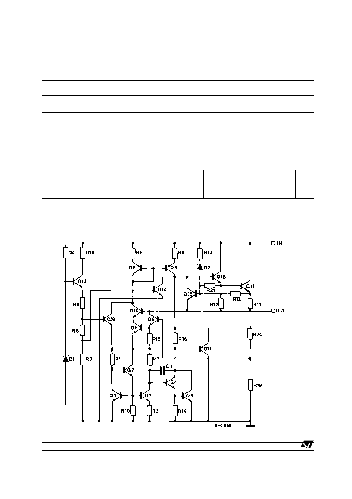
SCHEMATIC DIAGRAM
1/21March 2004
Page 2
L7800AB/AC S ER IES
ABSOLUTE MAXIMUM RATINGS
Symbol Parameter Value Unit
V
I
P
T
T
Absolute Maximum Ratings are those values beyond which damage to the device may occur. Functional operation under these condition is
not implied.
DC Input Voltage (for VO=5to18V)
I
Output Current
O
Power Dissipation
D
Storage Temperature Range
stg
Operating Junction Temperature Range (for L7800AC)
op
(for V
= 20, 24V)
O
(for L7800AB)
THERMAL DATA
35
40
V
V
Internally Limited mA
Internally Limited mW
-65 to +150 °C
0to+150
-40 to +125
°C
°C
Symbol Parameter TO-220 TO-220FP TO-220FM
R
thj-case
R
thj-amb
Thermal Resistance Junction-case
Thermal Resistance Junction-ambient
3553°C/W
50 60 60 62.5 °C/W
SHEMATIC DIAGRAM
2
D
PAK
Unit
2/21
Page 3
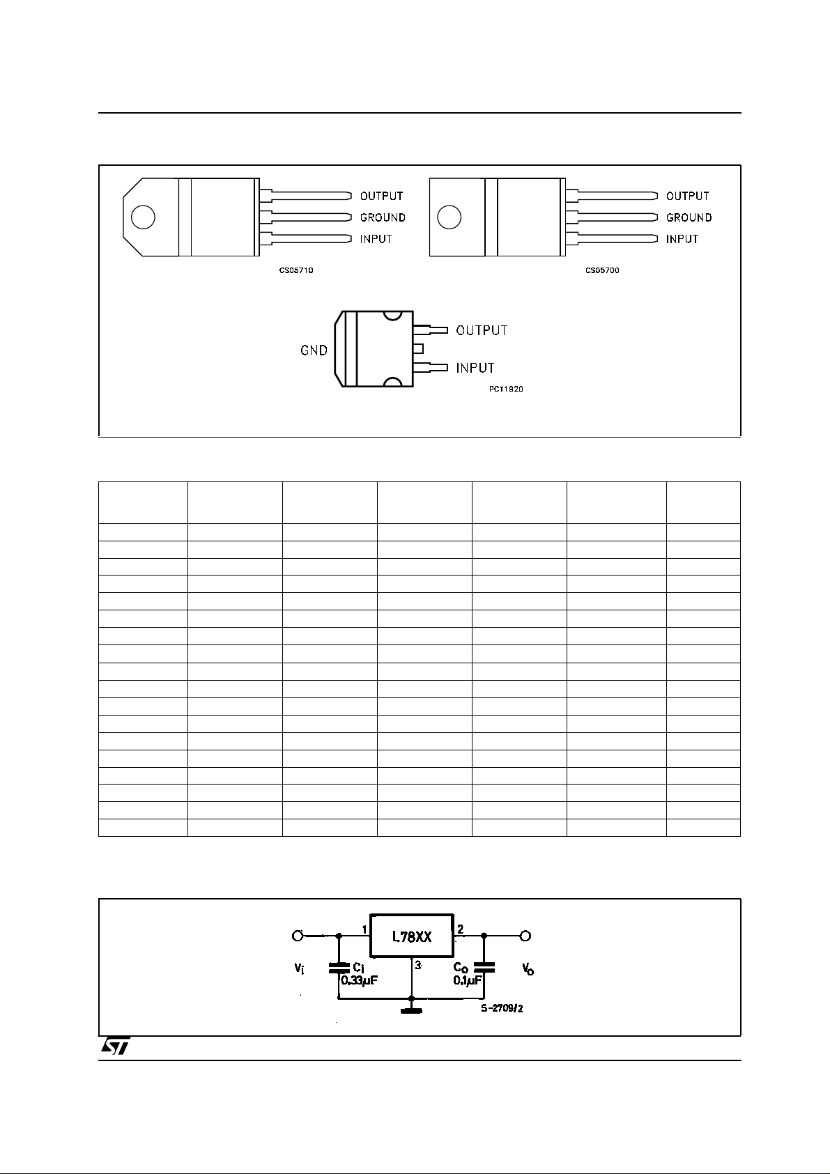
CONNECTION DIAGRAM (t op view)
L7800AB/AC SE RIES
TO-220 (Any Type)
TO-220FP/TO-220FM
D2PAK
ORDERING CODES
2
PAK
TYPE TO-220 TO-220FP TO-220FM
L7805AB L7805ABV L7805ABP L7805ABF L7805ABD2T 5 V
L7805AC L7805ACV L7805ACP L7805ACF L7805ACD2T L7805AC-D2TR 5 V
L7806AB L7806ABV L7806ABP L7806ABF L7806ABD2T 6 V
L7806AC L7806ACV L7806ACP L7806ACF L7806ACD2T 6 V
L7808AB L7808ABV L7808ABP L7808ABF L7808ABD2T 8 V
L7808AC L7808ACV L7808ACP L7808ACF L7808ACD2T 8 V
L7809AB L7809ABV L7809ABP L7809ABF L7809ABD2T 9 V
L7809AC L7809ACV L7809ACP L7809ACF L7809ACD2T 9 V
L7812AB L7812ABV L7812ABP L7812ABF L7812ABD2T 12 V
L7812AC L7812ACV L7812ACP L7812ACF L7812ACD2T 12 V
L7815AB L7815ABV L7815ABP L7815ABF L7815ABD2T 15 V
L7815AC L7815ACV L7815ACP L7815ACF L7815ACD2T 15 V
L7818AB L7818ABV L7818ABP L7818ABF L7818ABD2T 18 V
L7818AC L7818ACV L7818ACP L7818ACF L7818ACD2T 18 V
L7820AB L7820ABV L7820ABP L7820ABF L7820ABD2T 20 V
L7820AC L7820ACV L7820ACP L7820ACF L7820ACD2T 20 V
L7824AB L7824ABV L7824ABP L7824ABF L7824ABD2T 24 V
L7824AC L7824ACV L7824ACP L7824ACF L7824ACD2T 24 V
(*) Available in Tape & Reel with the suffix "-TR".
D
(A Type) (*)
D2PAK
(C Type) (T & R)
OUTPUT
VOLTAGE
APPLICATION CIRCUITS
3/21
Page 4
L7800AB/AC S ER IES
TEST CIRCUITS
Figure1 : DC Parameter
Figure2 : Load Regulation
Figure3 : Ripple Rejection
4/21
Page 5
L7800AB/AC SE RIES
ELECTRICAL CHARACTERISTICS OF L7805A (VI=10V, IO=1A, TJ= 0 to 150°C (L7805AC),
= -40 to 125°C (L7805AB), unless otherwise specified.)
T
J
Symbol Parameter Test Conditions Min. Typ. Max. Unit
V
Output Voltage TJ= 25°C 4.9 5 5.1 V
O
V
Output Voltage IO=5mAto1A PO≤ 15W
O
(*) Line Regulation VI= 7.5 to 25V IO= 500 mA 7 50 mV
∆V
O
(*) Load Regulation IO= 5mA to 1A 25 100 mV
∆V
O
Quiescent Current TJ= 25°C 4.3 6 mA
I
q
∆I
Quiescent Current Change VI=8to25V IO= 500 mA 0.8 mA
q
SVR Supply Voltage Rejection V
V
Dropout Voltage IO=1A TJ= 25°C 2 V
d
eN Output Noise Voltage T
R
Output Resistance f =1KHz 17 mΩ
O
Short Circuit Current VI= 35V TA=25°C 0.2 A
I
sc
I
Short Circuit Peak Current TJ= 25°C 2.2 A
scp
/∆T Output Voltage Drift -1.1 mv/°C
∆V
O
V
= 7.5 to 20V
I
V
=8to12V 10 50 mV
I
=8to12V TJ= 25°C 2 25 mV
V
I
= 7.3 to 20V TJ= 25°C 7 50 mV
V
I
I
=5mAto1.5A TJ= 25°C 30 100 V
O
= 250 to 750mA 8 50 V
I
O
= 7.5 to 20V TJ= 25°C 0.8 mA
V
I
I
=5mAto1A 0.5 mA
O
= 8 to 18V f = 120Hz
I
I
= 500mA
O
= 25°C B =10Hz to 100KHz 10 µV/V
A
4.8 5 5.2 V
6mA
68 dB
O
(*) Load and Line Regulation are specified atconstant junction temperature. Changes in VOdue to heating effects must be taken into account
separately. Pulse testing with low dutycycle is used.
5/21
Page 6

L7800AB/AC S ER IES
ELECTRICAL CHARACTERISTICS OF L7806A (VI=11V, IO=1A, TJ= 0 to 150°C (L7806AC),
= -40 to 125°C (L7806AB), unless otherwise specified.)
T
J
Symbol Parameter Test Conditions Min. Typ. Max. Unit
V
Output Voltage TJ= 25°C 5.88 6 6.12 V
O
V
Output Voltage IO=5mAto1A PO≤ 15W
O
(*) Line Regulation VI= 8.6 to 25V IO= 500 mA 9 60 mV
∆V
O
(*) Load Regulation IO= 5mA to 1A 25 100 mV
∆V
O
Quiescent Current TJ= 25°C 4.3 6 mA
I
q
∆I
Quiescent Current Change VI=9to25V IO= 500 mA 0.8 mA
q
SVR Supply Voltage Rejection V
Dropout Voltage IO=1A TJ= 25°C 2 V
V
d
eN Output Noise Voltage T
R
Output Resistance f =1KHz 17 mΩ
O
I
Short Circuit Current VI= 35V TA=25°C 0.2 A
sc
Short Circuit Peak Current TJ= 25°C 2.2 A
I
scp
/∆T Output Voltage Drift -0.8 mV/°C
∆V
O
(*) Load and Line Regulation are specified atconstant junction temperature. Changes in VOdue to heating effects must be taken into account
separately. Pulse testing with low dutycycle is used.
V
= 8.6 to 21V
I
V
=9to13V 11 60 mV
I
=9to13V TJ= 25°C 3 30 mV
V
I
= 8.3 to 21V TJ= 25°C 9 60 mV
V
I
I
=5mAto1.5A TJ= 25°C 30 100 V
O
= 250 to 750mA 10 50 V
I
O
= 8.6 to 21V TJ= 25°C 0.8 mA
V
I
I
=5mAto1A 0.5 mA
O
= 9 to 19V f = 120Hz
I
I
= 500mA
O
= 25°C B =10Hz to 100KHz 10 µV/V
A
5.76 6 6.24 V
6mA
65 dB
O
6/21
Page 7

L7800AB/AC SE RIES
ELECTRICAL CHARACTERISTICS OF L7808A (VI=14V, IO=1A, TJ= 0 to 150°C (L7808AC),
= -40 to 125°C (L7808AB), unless otherwise specified.)
T
J
Symbol Parameter Test Conditions Min. Typ. Max. Unit
V
Output Voltage TJ= 25°C 7.84 8 8.16 V
O
V
Output Voltage IO=5mAto1A PO≤ 15W
O
(*) Line Regulation VI= 10.6 to 25V IO= 500 mA 12 80 mV
∆V
O
(*) Load Regulation IO= 5mA to 1A 25 100 mV
∆V
O
Quiescent Current TJ= 25°C 4.3 6 mA
I
q
∆I
Quiescent Current Change VI=11to25V IO= 500 mA 0.8 mA
q
SVR Supply Voltage Rejection V
Dropout Voltage IO=1A TJ= 25°C 2 V
V
d
eN Output Noise Voltage T
R
Output Resistance f =1KHz 18 mΩ
O
I
Short Circuit Current VI= 35V TA=25°C 0.2 A
sc
Short Circuit Peak Current TJ= 25°C 2.2 A
I
scp
/∆T Output Voltage Drift -0.8 mV/°C
∆V
O
(*) Load and Line Regulation are specified atconstant junction temperature. Changes in VOdue to heating effects must be taken into account
separately. Pulse testing with low dutycycle is used.
V
=10.6 to 23V
I
V
= 11 to 17V 15 80 mV
I
=11to17V TJ= 25°C 5 40 mV
V
I
= 10.4 to 23V TJ= 25°C 12 80 mV
V
I
I
=5mAto1.5A TJ= 25°C 30 100 V
O
= 250 to 750mA 10 50 V
I
O
= 10.6 to 23V TJ= 25°C 0.8 mA
V
I
I
=5mAto1A 0.5 mA
O
= 11.5 to 21.5V f = 120Hz
I
I
= 500mA
O
= 25°C B =10Hz to 100KHz 10 µV/V
A
7.7 8 8.3 V
6mA
62 dB
O
7/21
Page 8

L7800AB/AC S ER IES
ELECTRICAL CHARACTERISTICS OF L7809A (VI=15V, IO=1A, TJ= 0 to 150°C (L7809AC),
= -40 to 125°C (L7809AB), unless otherwise specified.)
T
J
Symbol Parameter Test Conditions Min. Typ. Max. Unit
V
Output Voltage TJ= 25°C 8.82 9 9.18 V
O
V
Output Voltage IO=5mAto1A PO≤ 15W
O
(*) Line Regulation VI= 10.6 to 25V IO= 500 mA 12 90 mV
∆V
O
(*) Load Regulation IO= 5mA to 1A 25 100 mV
∆V
O
Quiescent Current TJ= 25°C 4.3 6 mA
I
q
∆I
Quiescent Current Change VI=11to25V IO= 500 mA 0.8 mA
q
SVR Supply Voltage Rejection V
Dropout Voltage IO=1A TJ= 25°C 2 V
V
d
eN Output Noise Voltage T
R
Output Resistance f =1KHz 18 mΩ
O
I
Short Circuit Current VI= 35V TA=25°C 0.2 A
sc
Short Circuit Peak Current TJ= 25°C 2.2 A
I
scp
/∆T Output Voltage Drift -0.8 mV/°C
∆V
O
(*) Load and Line Regulation are specified atconstant junction temperature. Changes in VOdue to heating effects must be taken into account
separately. Pulse testing with low dutycycle is used.
V
=10.6 to 23V
I
V
= 11 to 17V 15 90 mV
I
=11to17V TJ= 25°C 5 45 mV
V
I
= 10.4 to 23V TJ= 25°C 12 90 mV
V
I
I
=5mAto1.5A TJ= 25°C 30 100 V
O
= 250 to 750mA 10 50 V
I
O
= 10.6 to 23V TJ= 25°C 0.8 mA
V
I
I
=5mAto1A 0.5 mA
O
= 11.5 to 21.5V f = 120Hz
I
I
= 500mA
O
= 25°C B =10Hz to 100KHz 10 µV/V
A
8.65 9 9.35 V
6mA
61 dB
O
8/21
Page 9

L7800AB/AC SE RIES
ELECTRICAL CHARACTERISTICS OF L7812A (VI=19V, IO=1A, TJ= 0 to 150°C (L7812AC),
= -40 to 125°C (L7812AB), unless otherwise specified.)
T
J
Symbol Parameter Test Conditions Min. Typ. Max. Unit
V
Output Voltage TJ= 25°C 11.75 12 12.25 V
O
V
Output Voltage IO=5mAto1A PO≤ 15W
O
(*) Line Regulation VI= 14.8 to 30V IO= 500 mA 13 120 mV
∆V
O
(*) Load Regulation IO= 5mA to 1A 25 100 mV
∆V
O
Quiescent Current TJ= 25°C 4.4 6 mA
I
q
∆I
Quiescent Current Change VI= 15 to 30V IO= 500 mA 0.8 mA
q
SVR Supply Voltage Rejection V
Dropout Voltage IO=1A TJ= 25°C 2 V
V
d
eN Output Noise Voltage T
R
Output Resistance f =1KHz 18 mΩ
O
I
Short Circuit Current VI= 35V TA=25°C 0.2 A
sc
Short Circuit Peak Current TJ= 25°C 2.2 A
I
scp
/∆T Output Voltage Drift -1 mV/°C
∆V
O
V
=14.8 to 27V
I
V
= 16 to 22V 16 120 mV
I
= 16 to 22V TJ= 25°C 6 60 mV
V
I
= 14.5 to 27V TJ= 25°C 13 120 mV
V
I
I
=5mAto1.5A TJ= 25°C 30 100 V
O
= 250 to 750mA 10 50 V
I
O
= 14.8 to 27V TJ= 25°C 0.8 mA
V
I
I
=5mAto1A 0.5 mA
O
= 15 to 25V f = 120Hz
I
I
= 500mA
O
= 25°C B =10Hz to 100KHz 10 µV/V
A
11.5 12 12.5 V
6mA
60 dB
O
(*) Load and Line Regulation are specified atconstant junction temperature. Changes in VOdue to heating effects must be taken into account
separately. Pulse testing with low dutycycle is used.
9/21
Page 10
L7800AB/AC S ER IES
ELECTRICAL CHARACTERISTICS OF L7815A (VI=23V, IO=1A, TJ= 0 to 150°C (L7815AC),
= -40 to 125°C (L7815AB), unless otherwise specified.)
T
J
Symbol Parameter Test Conditions Min. Typ. Max. Unit
V
Output Voltage TJ= 25°C 14.7 15 15.3 V
O
V
Output Voltage IO=5mAto1A PO≤ 15W
O
(*) Line Regulation VI= 17.9 to 30V IO= 500 mA 13 150 mV
∆V
O
(*) Load Regulation IO= 5mA to 1A 25 100 mV
∆V
O
Quiescent Current TJ= 25°C 4.4 6 mA
I
q
∆I
Quiescent Current Change VI= 17.5 to 30V IO= 500 mA 0.8 mA
q
SVR Supply Voltage Rejection V
Dropout Voltage IO=1A TJ= 25°C 2 V
V
d
eN Output Noise Voltage T
R
Output Resistance f =1KHz 19 mΩ
O
I
Short Circuit Current VI= 35V TA=25°C 0.2 A
sc
Short Circuit Peak Current TJ= 25°C 2.2 A
I
scp
/∆T Output Voltage Drift -1 mV/°C
∆V
O
(*) Load and Line Regulation are specified atconstant junction temperature. Changes in VOdue to heating effects must be taken into account
separately. Pulse testing with low dutycycle is used.
V
= 17.9 to 30V
I
V
= 20 to 26V 16 150 mV
I
= 20 to 26V TJ= 25°C 6 75 mV
V
I
= 17.5 to 30V TJ= 25°C 13 150 mV
V
I
I
=5mAto1.5A TJ= 25°C 30 100 V
O
= 250 to 750mA 10 50 V
I
O
= 17.5 to 30V TJ= 25°C 0.8 mA
V
I
I
=5mAto1A 0.5 mA
O
= 18.5 to 28.5V f = 120Hz
I
I
= 500mA
O
= 25°C B =10Hz to 100KHz 10 µV/V
A
14.4 15 15.6 V
6mA
58 dB
O
10/21
Page 11

L7800AB/AC SE RIES
ELECTRICAL CHARACTERISTICS OF L7818A (VI=27V, IO=1A, TJ= 0 to 150°C (L7818AC),
= -40 to 125°C (L7818AB), unless otherwise specified.)
T
J
Symbol Parameter Test Conditions Min. Typ. Max. Unit
V
Output Voltage TJ= 25°C 17.64 18 18.36 V
O
V
Output Voltage IO=5mAto1A PO≤ 15W
O
(*) Line Regulation VI= 21 to 33V IO= 500 mA 25 180 mV
∆V
O
(*) Load Regulation IO= 5mA to 1A 25 100 mV
∆V
O
Quiescent Current TJ= 25°C 4.5 6 mA
I
q
∆I
Quiescent Current Change VI= 21 to 33V IO= 500 mA 0.8 mA
q
SVR Supply Voltage Rejection V
Dropout Voltage IO=1 A TJ= 25°C 2 V
V
d
eN Output Noise Voltage T
R
Output Resistance f =1KHz 19 mΩ
O
I
Short Circuit Current VI= 35V TA=25°C 0.2 A
sc
Short Circuit Peak Current TJ= 25°C 2.2 A
I
scp
/∆T Output Voltage Drift -1 mV/°C
∆V
O
(*) Load and Line Regulation are specified atconstant junction temperature. Changes in VOdue to heating effects must be taken into account
separately. Pulse testing with low dutycycle is used.
V
= 21 to 33V
I
V
= 24 to 30V 28 180 mV
I
= 24 to 30V TJ= 25°C 10 90 mV
V
I
= 20.6 to 33V TJ= 25°C 5 180 mV
V
I
I
=5mAto1.5A TJ= 25°C 30 100 V
O
= 250 to 750mA 10 50 V
I
O
= 21 to 33V TJ= 25°C 0.8 mA
V
I
I
=5mAto1A 0.5 mA
O
= 22 to 32V f = 120Hz
I
I
= 500mA
O
= 25°C B =10Hz to 100KHz 10 µV/V
A
17.3 18 18.7 V
6mA
57 dB
O
11/21
Page 12

L7800AB/AC S ER IES
ELECTRICAL CHARACTERISTICS OF L7820A (VI=28V, IO=1A, TJ= 0 to 150°C (L7820AC),
= -40 to 125°C (L7820AB), unless otherwise specified.)
T
J
Symbol Parameter Test Conditions Min. Typ. Max. Unit
V
Output Voltage TJ= 25°C 19.6 20 20.4 V
O
V
Output Voltage IO=5mAto1A PO≤ 15W
O
(*) Line Regulation VI= 23 to 35V IO= 500 mA 200 mV
∆V
O
(*) Load Regulation IO= 5mA to 1A 25 100 mV
∆V
O
Quiescent Current TJ= 25°C 4.5 6 mA
I
q
∆I
Quiescent Current Change VI= 23 to 35V IO= 500 mA 0.8 mA
q
SVR Supply Voltage Rejection V
Dropout Voltage IO=1 A TJ= 25°C 2 V
V
d
eN Output Noise Voltage T
R
Output Resistance f =1KHz 20 mΩ
O
I
Short Circuit Current VI= 35V TA=25°C 0.2 A
sc
Short Circuit Peak Current TJ= 25°C 2.2 A
I
scp
/∆T Output Voltage Drift -1 mV/°C
∆V
O
V
= 23 to 35V
I
V
= 26 to 32V 200 mV
I
= 26 to 32V TJ= 25°C 100 mV
V
I
= 23 to 32V TJ= 25°C 200 mV
V
I
I
=5mAto1.5A TJ= 25°C 30 100 V
O
= 250 to 750mA 10 50 V
I
O
= 23 to 35V TJ= 25°C 0.8 mA
V
I
I
=5mAto1A 0.5 mA
O
= 24 to 35V f = 120Hz
I
I
= 500mA
O
= 25°C B =10Hz to 100KHz 10 µV/V
A
19.2 20 20.8 V
6mA
56 dB
O
(*) Load and Line Regulation are specified atconstant junction temperature. Changes in VOdue to heating effects must be taken into account
separately. Pulse testing with low dutycycle is used.
12/21
Page 13

L7800AB/AC SE RIES
ELECTRICAL CHARACTERISTICS OF L7824A (VI=33V, IO=1A, TJ= 0 to 150°C (L7824AC),
= -40 to 125°C (L7824AB), unless otherwise specified.)
T
J
Symbol Parameter Test Conditions Min. Typ. Max. Unit
V
Output Voltage TJ= 25°C 23.5 24 24.5 V
O
V
Output Voltage IO=5mAto1A PO≤ 15W
O
(*) Line Regulation VI= 27 to 38V IO= 500 mA 31 240 mV
∆V
O
(*) Load Regulation IO= 5mA to 1A 25 100 mV
∆V
O
Quiescent Current TJ= 25°C 4.6 6 mA
I
q
∆I
Quiescent Current Change VI= 27.3 to 38V IO= 500 mA 0.8 mA
q
SVR Supply Voltage Rejection V
Dropout Voltage IO=1 A TJ= 25°C 2 V
V
d
eN Output Noise Voltage T
R
Output Resistance f =1KHz 20 mΩ
O
I
Short Circuit Current VI= 35V TA=25°C 0.2 A
sc
Short Circuit Peak Current TJ= 25°C 2.2 A
I
scp
/∆T Output Voltage Drift -1.5 mV/°C
∆V
O
(*) Load and Line Regulation are specified atconstant junction temperature. Changes in VOdue to heating effects must be taken into account
separately. Pulse testing with low dutycycle is used.
V
= 27.3 to 38V
I
V
= 30 to 36V 35 240 mV
I
= 30 to 36V TJ= 25°C 14 120 mV
V
I
= 26.7 to 38V TJ= 25°C 31 240 mV
V
I
I
=5mAto1.5A TJ= 25°C 30 100 V
O
= 250 to 750mA 10 50 V
I
O
= 27.3 to 38V TJ= 25°C 0.8 mA
V
I
I
=5mAto1A 0.5 mA
O
= 28 to 38V f = 120Hz
I
I
= 500mA
O
= 25°C B =10Hz to 100KHz 10 µV/V
A
23 24 25 V
6mA
54 dB
O
13/21
Page 14

L7800AB/AC S ER IES
APPLICATION INFORMATION
DESIGN CONSIDERATION
The L7800A Series of fixed voltage regulators are
designed with Th ermal Overload Protection that
shuts down the circuit when subje cted to an
excessive power overload condition, Internal
Short-circuit Protection that limits the maximum
current the circuit will pass, and Output transistor
Safe-Area Compensation that reduc es the output
short-circuit current as the voltage across the pass
transistor is in crea se d. In many low current
applications, compensation capac itor s are not
required. However, it is recommended that the
regulator input be bypassed with capacitor if the
regulator is connected to the power supply filter
with long lengths, or if the output load capacitance
is large. A n input bypass capacitor should be
selected to provide good high frequency
characteristics to insure stable operation under all
load conditions. A 0.33mF or larger tantalum,
mylar or other capacitor having low i nterna l
impedance at high frequencies should be chosen.
The bypass capacitor should be mounted with the
shortest possible leads directly across the
regulators input terminals. Normally good
construction techniques should be used to
minimize ground loops and lead resistance drops
since the regulator has no external sense lead.
The addition of an operational amplifier allows
adjustment to higher or intermediate v alues while
retaining regulation characteristics. The minimum
voltage obtained with the arrangement is 2V
greater than the regulator voltage.
The circuit of figure 6 can be modified to provide
supply protection against short circuit by adding a
short circuit sense resistor, RSC, and an
additional PNP transistor. T he current sensing
PNP must be able to handle the short c ircuit
current of the three terminal regulator Therefore a
four ampere plastic power transistor is specified.
Figure5 : DC Parameter
VO, 7.0 to 20V
VI-VO≥ 2.0V
Figure6 : DC Parameter
V
R1=
IO=I
BEQ1
I
Q1
I
-
REQ
β
Q1
REG+Q1(IREG
V
BEQ1
)
R
Figure7 : DC Parameter
1
Figure4 : DC Parameter
V
xx
IO= +I
14/21
d
R
1
Page 15

L7800AB/AC SE RIES
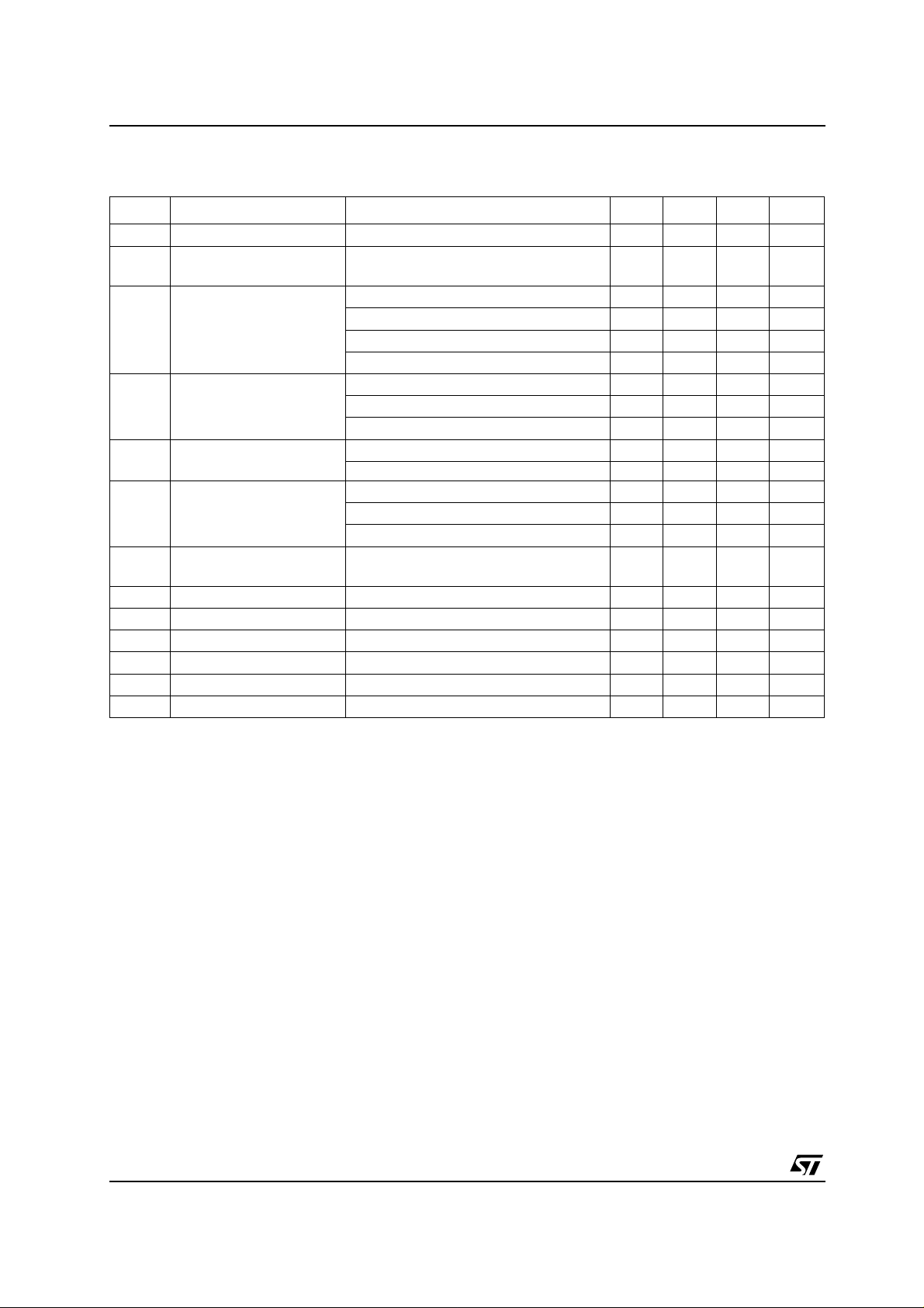
TO-220 MECHANICAL DAT
DIM.
A 4.40 4.60 0.173 0.181
C 1.23 1.32 0.048 0.051
D 2.40 2.72 0.094 0.107
D1 1.27 0.050
E 0.49 0.70 0.019 0.027
F 0.61 0.88 0.024 0.034
F1 1.14 1.70 0.044 0.067
F2 1.14 1.70 0.044 0.067
G 4.95 5.15 0.194 0.203
G1 2.4 2.7 0.094 0.106
H2 10.0 10.40 0.393 0.409
L2 16.4 0.645
L4 13.0 14.0 0.511 0.551
L5 2.65 2.95 0.104 0.116
L6 15.25 15.75 0.600 0.620
L7 6.2 6.6 0.244 0.260
L9 3.5 3.93 0.137 0.154
DIA. 3.75 3.85 0.147 0.151
MIN. TYP MAX. MIN. TYP. MAX.
mm. inch
A
P011C
15/21
Page 16

L7800AB/AC S ER IES
TO-220FP MECHANICAL DATA
DIM.
A 4.40 4.60 0.173 0.181
B 2.5 2.7 0.098 0.106
D 2.5 2.75 0.098 0.108
E 0.45 0.70 0.017 0.027
F 0.75 1 0.030 0.039
F1 1.15 1.50 0.045 0.059
F2 1.15 1.50 0.045 0.059
G 4.95 5.2 0.194 0.204
G1 2.4 2.7 0.094 0.106
H 10.0 10.40 0.393 0.409
L2 16 0.630
L3 28.6 30.6 1.126 1.204
L4 9.8 10.6 0.385 0.417
L6 15.9 16.4 0.626 0.645
L7 9 9.3 0.354 0.366
DIA. 3 3.2 0.118 0.126
MIN. TYP MAX. MIN. TYP. MAX.
mm. inch
A
B
H
E
D
L3
L6
L7
¯
F1
F
G1
G
F2
123
L2
L4
7012510/G
16/21
Page 17

TO-220FM MECHANICAL DATA
L7800AB/AC SE RIES
DIM.
A 4.50 4.90 0.177 0.193
B 3.04 3.44 0.120 0.135
D 2.56 2.96 0.101 0.117
E 0.45 0.50 0.60 0.018 0.020 0.024
F 0.70 0.90 0.028 0.035
F1 1.47 0.058
G 5.08 0.200
G1 2.34 2.54 2.74 0.092 0.100 0.108
H 9.96 10.36 0.392 0.408
L2 15.8 0.622
L4 9.45 10.05 0.372 0.396
L6 15.67 16.07 0.617 0.633
L7 8.99 9.39 0.354 0.370
L8 3.30 0.130
DIA. 3.08 3.28 0.121 0.129
MIN. TYP MAX. MIN. TYP. MAX.
mm. inch
7012510C/G
17/21
Page 18

L7800AB/AC S ER IES
D2PAK (A TYPE) MECHANICAL DATA
mm. inch
DIM.
MIN. TYP MAX. MIN. TYP. MAX.
A 4.4 4.6 0.173 0.181
A1 0.03 0.23 0.001 0.009
b 0.7 0.93 0.027 0.036
b2 1.14 1.7 0.044 0.067
c 0.45 0.6 0.017 0.023
c2 1.23 1.36 0.048 0.053
D 8.95 9.35 0.352 0.368
D1
E 10 10.4 0.393 0.409
E1 8.5 0.335
e 2.54 0.100
e1 4.88 5.28 0.192 0.208
H 15 15.85 0.590 0.624
J1 2.49 2.69 0.098 0.106
L 2.29 2.79 0.090 0.110
L1 1.27 1.4 0.050 0.055
L2 1.3 1.75 0.051 0.069
R 0.4 0.016
V2 0° 8° 0° 8°
8
0.315
18/21
0079457/I
Page 19
L7800AB/AC SE RIES
D2PAK (C TYPE) MECHANICAL DATA
mm. inch
DIM.
MIN. TYP MAX. MIN. TYP. MAX.
A 4.3 4.7 0.169 0.185
A1 0 0.20 0.000 0.008
b 0.70 0.90 0.028 0.035
b2 1.17 1.37 0.046 0.054
c 0.45 0.50 0.6 0.018 0.020 0.024
c2 1.25 1.30 1.40 0.049 0.051 0.055
D 9.0 9.2 9.4 0.354 0.362 0.370
D1 7.5 0.295
E 9.8 10.2 0.386 0.402
E1 7.5 0.295
e 2.54 0.100
e1 5.08 0.200
H 15 15.30 15.60 0.591 0.602 0.614
J1 2.20 2.60 0.087 0.102
L 1.79 2.79 0.070 0.110
L1 1.0 1.4 0.039 0.055
L2 1.2 1.6 0.047 0.063
R 0.3 0.012
V2 0° 3° 0° 3°
0079457/I
19/21
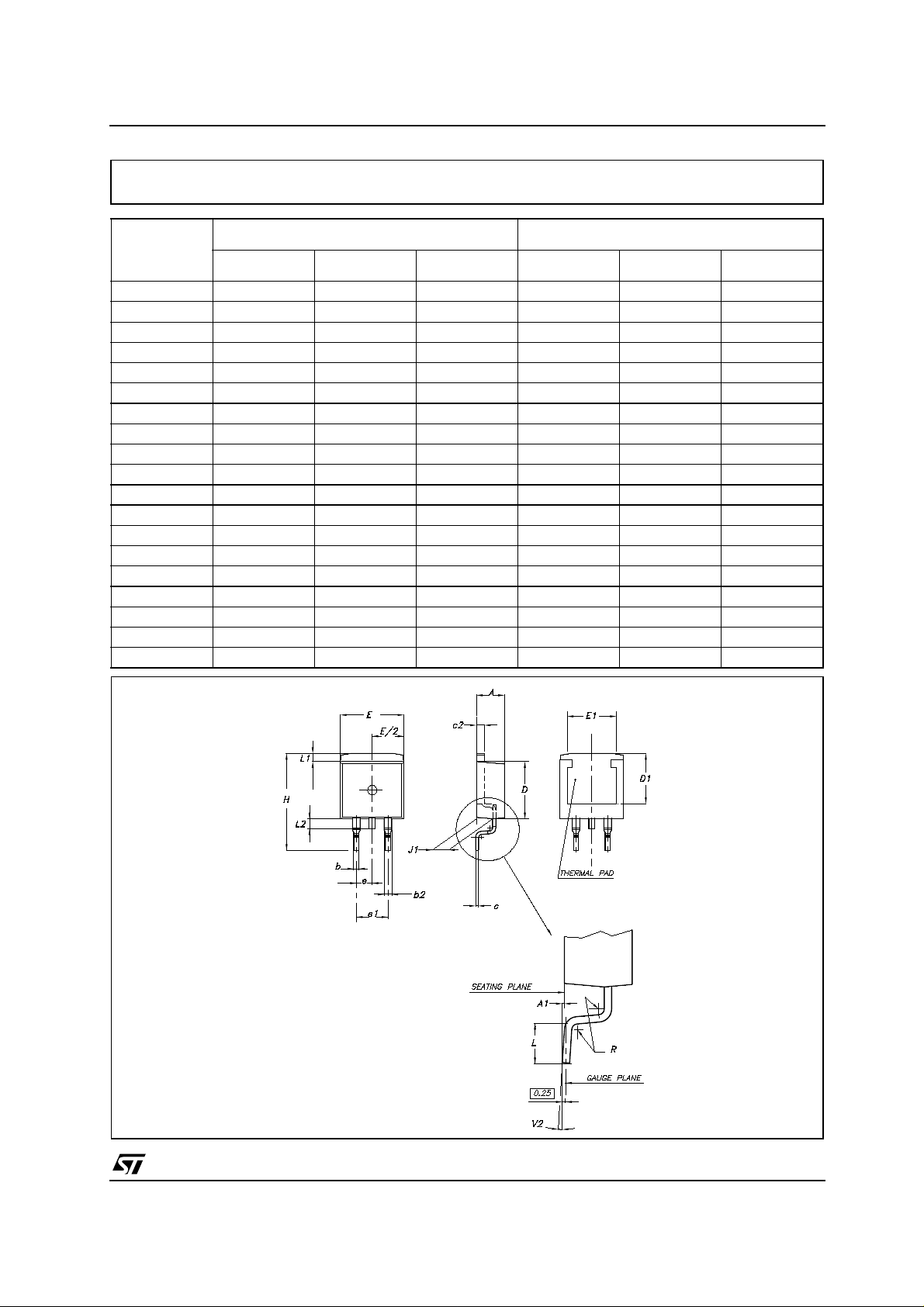
Page 20
L7800AB/AC S ER IES
Tape & Reel D
DIM.
A 180 7.086
C 12.8 13.0 13.2 0.504 0.512 0.519
D 20.2 0.795
N 60 2.362
T 14.4 0.567
Ao 10.50 10.6 10.70 0.413 0.417 0.421
Bo 15.70 15.80 15.90 0.618 0.622 0.626
Ko 4.80 4.90 5.00 0.189 0.193 0.197
Po 3.9 4.0 4.1 0.153 0.157 0.161
P 11.9 12.0 12.1 0.468 0.472 0.476
2
PAK-P2PAK-D2PAK/A-P2PAK/A MECHANICAL DATA
mm. inch
MIN. TYP MAX. MIN. TYP. MAX.
20/21
Page 21

L7800AB/AC SE RIES
Information furnished is believed to be accurate and reliable. However, STMicroelectronics assumes no responsibility for the
consequences of use of such inform ation nor fo r an y infring ement of p atents or o ther rights of third p arties which may r esult f rom
its use. No license is granted by implication or otherwise under any patent or patent rights of STMicroelectronics. Specifications
mentioned in this publication are subject to change without notice. This publication supersedes and replaces all information
previously supplied. STMicroelectronics products are not authorized for use as critical components in life support devices or
systems without express written approval of STMicroelectronics.
Australia - Belgium - Brazil - Canada - China - Czech Republic - Finland - France - Germany - Hong Kong - India - Israel - Italy - Japan -
Malaysia - Malta - Morocco - Singapore - Spain - Sweden - Switzerland - United Kingdom - United States.
The ST logo is a registered trademark of STMicroelectronics
All other names are the property of their respective owners
© 2004 STMicroelectronics - All Rights Reserved
STMicroelectronics GROUP OF COMPANIES
http://www.st.com
21/21
 Loading...