

Page 1

L6258E
Fi
PWM CONTROLLED - HIGH CURRENT
DMOS UNIVERSAL MOTOR DRIVER
NOT FOR NEW DESIGN
1 FEATURES
■ ABLE TO DRIVE BOTH WINDINGS OF A
BIPOLAR STEPPER MOTOR OR TWO DC
MOTORS
■ OUTPUT CURRENT UP TO 1.2A EACH
WINDING
■ WIDE VOLTAGE RANGE: 12V TO 40V
■ FOUR QUADRANT CURRENT CONTROL,
IDEAL FOR MICROSTEPPING AND DC
MOTOR CONTROL
■ PRECISION PWM CONTROL
■ NO NEED FOR RECIRCULATION DIODES
■ TTL/CMOS COMPATIBLE INPUTS
■ CROSS CONDUCTION PROTECTION
■ THERMAL SHUTDOW
2 DESCRIPTION
L6258E is a dual full bridge for mot or control appl ications realized in BCD technology, with the capability
of driving both windings of a bipolar s tepper motor or
bidirectionally control two DC motors.
L6258E and a few external components form a com-
Figure 2. Block Diagram
INPUT
&
SENSE
AMP
INPUT
&
SENSE
AMP
EA_IN1 EA_OUT1VCP2
THERMAL
EA_IN2 EA_OUT2GND
PROT.
VDD(5V)
VCP1
VREF1
PH_1
VREF1
PH_2
TRI_CAP
C
FREF
I3_1
I2_1
I1_1
I0_1
I3_2
I2_2
I1_2
I0_2
C
CHARGE
PUMP
DAC
VR GEN
DAC
TRIANGLE
GENERATOR
P
VR (VDD/2)
TRI_0
TRI_180
gure 1. Package
PowerSO36
Table 1. Order Codes
Part Number Package
L6258E
PowerSO36
(Replaced by L6258EX)
plete control and drive circuit. It has high efficiency
phase shift chopping that allows a very low current
ripple at the lowest current contr ol lev els , and ma kes
this device ideal for steppers as well as for DC motors.The power stage is a dual DMOS full bridge capable of sustaining up to 40V, and includes the
diodes for current recirculation.The o utput current capability is 1.2A per winding in continuous mode, with
peak start-up current up to 1.5A. A thermal protectio n
circuitry disables the outputs if the chip temperature
exceeds the safe limits.
R
1M
1
C
C1
R
C1
TRI_0
+
C
TRI_180
C2
TRI_0
TRI_180
-
+
C
-
+
C
-
+
C
-
ERROR
V
R
AMP
+
-
ERROR
V
R
AMP
+
-
R
C2
C
R
1M
2
VS
POWER
BRIDGE
C
1
POWER
BRIDGE
2
BOOT
VBOOT
D96IN430D
OUT1A
OUT1B
SENSE1B
SENSE1A
DISABLE
VS
OUT2A
OUT2B
SENSE2B
SENSE2A
R
s
R
s
September 2004
Rev. 7
1/24
Page 2

L6258E
Table 2. Absolute Maximum Ratings
Symbol Parameter Value Unit
V
V
DD
V
ref1/Vref2
I
O
I
O
V
V
boot
V
boot
T
T
stg
in
Supply Voltage 45 V
s
Logic Supply Voltage 7 V
Reference Voltage 2.5 V
Output Current (peak) 1.5 A
Output Current (continuous) 1.2 A
Logic Input Voltage Range -0.3 to 7 V
Bootstrap Supply 60 V
- VsMaximum Vgate applicable 15 V
Junction Temperature 150 °C
j
Storage Temperature Range -55 to 150 °C
Figure 3. Pin Connection (Top view)
PWR_GND
PH_1
I1_1
I0_1
OUT1A
DISABLE
TRI_CAP
V
GND
VCP1
VCP2
VBOOT
OUT2A
I0_2
I1_2
PH_2
PWR_GND
VS
1
2
3
4
5
6
7
DD
8
9
10
11
12
13 24
14
15
16
17
18
36
35
34
33
32
31
30
29
28
27
26
25
23
22
21
20
19
PWR_GND
SENSE1
OUT1B
I3_1
I2_1
VS
EA_OUT1
EA_IN1
VREF1
SIG_GND
VREF2
EA_IN2
EA_OUT2
I2_2
I3_2
OUT2B
SENSE2
PWR_GND
2/24
D96IN432E
Page 3

Table 3. Pins Function
Pin # Name Description
1, 36 PWR_GND Ground connection (1). They also conduct heat from die to printed circuit copper.
2, 17 PH_1, PH_2 These TTL compatible logic inputs set the direction of current flow through the load. A
3I
4I
1_1
0_1
5 OUT1A Bridge output connection (1)
6 DISABLE Disables the bridges for additional safety during switching. When not connected the
7 TRI_cap Triangular wa v e gen er ati on ci rc uit ca pac ito r. The value of thi s ca paci tor def ine s th e ou tput
8V
(5V) Supply Voltage Input for logic circuitry
DD
9 GND Power Ground connection of the internal charge pump circuit
10 V
11 V
12 V
13, 31 V
CP1
CP2
BOOT
S
14 OUT2A Bridge output connection (2)
15 I
16 I
0_2
1_2
18, 19 PWR_GND Ground connection. They also conduct heat from die to printed circuit copper
20, 35 SENSE2,
SENSE1
21 OUT2B Bridge output connection and positive input of the tranconductance (2)
22 I
23 I
3_2
2_2
24 EA_OUT_2 Error amplifier output (2)
25 EA_IN_2 Negative input of error amplifier (2)
26, 28 V
REF2
, V
27 SIG_GND Signal ground connection
29 EA_IN_1 Negative input of error amplifier (1)
30 EA_OUT_1 Error amplifier output (1)
32 I
33 I
2_1
3_1
34 OUT1B Bridge output connection and positive input of the tranconductance (1)
Note: The number in parenthesis shows the relevant Power Bridge of the circuit. Pins 18, 19, 1 and 36 are connected together.
high level causes current to flow from OUTPUT A to OUTPUT B.
Logic input of the internal DAC (1). The output voltage of the DAC is a percentage of the
Vref voltage applied according to the thruth table of page 7
See pin 3
bridges are enabled
switching frequency
Charge pump oscillator output
Input for external charge pump capacitor
Overvoltage input for driving of the upper DMOS
Supply voltage input for output stage. They are shorted intern ally
Logic input of the internal DAC (2). The output voltage of the DAC is a percentage of the
VRef voltage applied accordin g to the tr uth table of page 7
See pin 15
Negative input of the transconductance input amplifier (2, 1)
See pin 15
See pin 15
Reference voltages for the internal DACs, determining the output current value. Output
REF1
current also depends on the logic inputs of the DAC and on the sensing resistor value
See pin 3
See pin 3
L6258E
3/24
Page 4

L6258E
Figure 4. Thermal Characteristics
Conditions
pad layout + ground layers + 16 via hol
PCB ref.: 4 LAYER cm 12 x 12
pad layout + ground layers
PCB ref.: 4 LAYER cm 12 x 12
pad layout + 6cm2 on board heat sink
PCB ref.: 2 LAYER cm 12 x 12
12
10
8
20˚C/W
6
4
Power Dissipated (W)
2
Power Dissipated
(W)
5.3 70 15
4.0 70 20
2.3 70 35
15˚C/W
35˚C/W
T Ambient
(˚C)
Thermal J-A resistance
(˚C/W)
D02IN1370
4/24
0
0
20 40 60 80 100 120 140 160
Ambient Temperature (˚C)
D02IN1371
Page 5

L6258E
Table 4. Electrical Characteristics (VS = 40V; VDD = 5V; Tj = 25°; unless otherwise specif ied .)
Symbol Parameter Test Condition Min. Typ. Max. Unit
V
Supply Voltage 12 40 V
S
V
V
BOOT
V
Sense
V
S(off)
V
DD(off)
I
S(on)
I
S(off)
I
∆T
T
f
TRANSISTORS
I
DSS
R
ds(on)
CONTROL LOGIC
V
V
I
V
ref1/ref2
I
FI =
V
ref/Vsense
V
V
offset
SENSE AMPLIFIER
V
I
ERROR AMPLIFIER
G
SR Output Slew Rate Open Loop 0.2 V/µs
GBW Gain Bandwidth Product 400 kHz
Note 1: This is true for all the logic inputs except the disable input.
(*) Chopping frequency is twice fosc value.
Logic Supply Voltage 4.75 5.25 V
DD
Storage Voltage VS = 12 to 40V VS+6 VS+12 V
Max Drop Across Sense Resistor 1.25 V
Power off Reset Off Threshold 6 7.2 V
Power off Reset Off Threshold 3.3 4.1 V
VS Quiescent Current Both bridges ON, No Load 15 mA
VS Quiescent Current Both bridges OFF 7 mA
VDD Operative Current 15 mA
DD
Shut Down Hysteresis 25 °C
SD-H
Thermal shutdown 150 °C
SD
Triangular Oscillator Frequency
osc
(*)CFREF
= 1nF 12.5 15 18.5 KHz
Leakage Current OFF State 500 µA
On Resistance ON State 0.6 0.75 Ω
Flywheel diode Voltage If =1.0A 1 1.4 V
V
f
lnput Voltage All Inputs 2 V
in(H)
Input Voltage All Inputs 0 0.8 V
in(L)
Input Current (Note 1) 0 < Vin < 5V -150 +10 µA
I
in
Disable Pin Input Current -10 +150 µA
dis
Reference Voltage operating 0 2.5 V
V
ref
Terminal Input Current V
ref
= 1.25 -2 5 µA
ref
PWM Loop Transfer Ratio 2
DAC Full Scale Precision V
FS
Current Loop Offset V
= 2.5V I0/I1/I2/I3 = L 1.23 1.34 V
ref
= 2.5V I0/I1/I2/I3 = H -30 +30 mV
ref
DAC Factor Ratio Normalized @ Full scale Value -2 +2 %
lnput Common Mode Voltage
cm
-0.7 VS+0.7 V
Range
Input Bias sense1/sense2 -200 0 µA
inp
Open Loop Voltage Gain 70 dB
V
DD
V
5/24
Page 6

L6258E
3 FUNCTIONAL DESCRIPTION
The circuit is intended to drive both windings of a bipolar stepper motor or two DC motors.
The current control is generated through a switch mode regulation.
With this system the direct ion and the ampl itud e of the load current are depending on the r el ation of phas e and
duty cycle between the two outputs of the current control loop.
The L6258E power stage is composed by power DMOS in bridge confi guration as it is shown in figure 5, wher e
the bridge outputs OUT_A and OUT_B are driven to V
driven to ground with a low level at the same inputs .
The zero current condition is obtained by driving the two half bridge us ing si gnals I N_A and IN_B with the same
phase and 50% of duty cycle.
In this case the outputs of the two half bridges are continuously switched between power supply (V
ground, but keeping the differential voltage across the load equal to zero.
In figure 5A is shown the timing diagram of the two outputs and the load current for this working condition.
Following we consider positive the current flowing into the load with a direction from OUT_A to OUT_B, while
we consider negative the current flowing into load with a direction from OUT_B to OUT_A.
Now just increasing the duty cycle of the IN_A signal and decreasi ng the duty c ycle of IN_B s ignal we driv e pos-
itive current into the load.
In this way the two outputs are not in phase, and the current can flow into the load trough the diagonal bridge
formed by T1 and T4 when the output OUT_A is driven to V
there will be a current r eci rculati on into the higher side of the bri dge, th rough T1 an d T2, when both the outputs
are at Vs and a current recir culation int o the l ower si de of the br idge, through T3 and T4, when both the outputs
are connected to ground.
Since the voltage applied to the load for r ecirculation is low, the res ulting current discharge time cons tant is higher than the current charging time cons tant dur ing the per iod in whi ch th e cur rent fl ows i nto the l oad thr ough th e
diagonal bridge formed by T1 and T4. In this way the load current will be positive with an average amplitude
depending on the difference in duty cycle of the two driving signals.
In figure 5B is shown the timing diagram in the case of positive load current
On the contrary, if we want to drive negative curr ent into the load is necessary to decrease the du ty cycle of th e
IN_A signal and increase the duty cycle of the IN_B signal. In this way we obtain a phase shift between the two
outputs such to have current flowing into the diagonal bridge formed by T2 and T3 when the output OUT_A is
driven to ground and output OUT_B is driven to V s, while we wi ll hav e the sam e current recirculati on condit ions
of the previous case when both the outputs are driven to Vs or to ground.
So, in this case the load current will be negativ e with an average ampl itude always depending by th e difference
in duty cycle of the two driving signals.
In figure 5C is shown the timing diagram in the case of negative load current .
Figure 6 shows the device block diagram of the complete current control loop.
with an high level a t the inpu ts IN_A and IN_B whi le ar e
s
) and
s
and the output OUT_B is driven to ground, while
s
3.1 Reference Voltage
The voltage applied to VREF pi n i s t he r efer ence for the i nternal DAC and, together with the sen se res istor val ue, defines the maximum current into the motor winding according to the following relation:
V
1
-----
--------------
⋅==
FI
REF
R
S
where R
6/24
= sense resistor value
s
I
MAX
0.5 V
⋅
REF
-------------------------- -
R
S
Page 7

Figure 5. Power Bridge Configuration
L6258E
V
S
OUTA
OUTB
Iload
OUTA
IN_A IN_B
0
T1
OUT_A OUT_B
T3
LOAD
T2
T4
Fig. 1A
OUTB
Iload
OUTA
OUTB
Iload
Fig. 1B
0
Fig. 1C
0
D97IN624
7/24
Page 8

L6258E
Figure 6. Current Control Loop Block Diagram
VREF
PH
INPUT TRANSCONDUCTANCE
I0
I1
I2
I3
DAC
VDAC
AMPL.
ia
+
-
Gin=1/Ra
ERROR AMPL.
V
R
+
ic
Rc
Cc
ib
VSENSE
+
Gs=1/Rb
SENSE TRANSCONDUCTANCE
AMPL.
Tri_0
Tri_180
-
+
-
+
POWER AMPL.
VS
VS
OUTA
OUTB
D97IN625
LOAD
R
L
L
L
R
S
3.2 Input Logic (I
- I1 - I2 - I3)
0
The current level in the motor winding is selected according to this table:
Table 5.
I3 I2 I1 I0
HHHH No Current
HHHL 9.5
HHLH 19.1
HHLL 28.6
HLHH 38.1
HLHL 47.6
HLLH 55.6
HLLL 63.5
LHHH 71.4
LHHL 77.8
LHLH 82.5
LHLL 88.9
LLHH 92.1
LLHL 95.2
LLLH 98.4
LLLL 100
Current level
% of IMAX
8/24
Page 9

L6258E
3.3 Phase Input ( PH )
The logic level applied to this input determines the direction of the current flowing in the winding of the motor.
High level on the phase input causes the motor current flowing from OUT_A to OUT_B through the load.
3.4 Triangular Generator
This circuit generates the two triangular waves TRI_0 and TRI_180 internally used to generate the duty cycle
variation of the signals driving the output stage in bridge configuration.
The frequency o f th e tri an gular wave defines the s wi tc hing frequency of the output, and can be ad justed by chang ing
the capacitor connected at TR1_CAP pin :
ref
K
--- -=
C
where : K = 1.5 x 10
F
-5
3.5 Charge Pump Circuit
To ensure the correct driving of t he high sid e drivers a vo ltage higher than Vs i s supplied on the V boot pin. This
boostrap voltage is not needed for the low side power DMOS transistors because their sources terminals are
grounded. To produce this voltage a char ge pump method is used. It is made by usi ng two ex ternal capacitors;
one connected to the internal oscillator (CP) and the other (Cboot) to storage the overvoltage needed for the
driving the gates of the high side DMOS. The value suggested for the capacitors are:
Table 6.
C
boot
C
P
Storage Capacitor 100 nF
PumpCapacitor 10 nF
3.6 Current Control LOOP
The current control loop is a transconductance amplifier working in PWM mode.
The motor current is a function of the programmed DAC voltage.
To keep under control the output current, the curr ent control modulates the duty c ycle of the two outputs OUT_A
and OUT_B, and a sensing resi stor Rs is c onnect ed in series with the motor win ding in or der to prod uce a vol t age feedback compared with the programmed voltage of the DAC .
The duty cycle modulation of the two outputs is generated comparing the voltage at the outputs of the error amplifier, with the two triangular wave references .
In order to drive the output bridge wi th the duty c ycle modula tion expla ined be fore, the signal s dri ving each output ( OUTA & OUTB ) are generated b y the use of the two comparators having as refer ence two triangul ar wave
signals Tri_0 and Tri_180 of the same amplitude, the same average value (in our case Vr), but with a 180° of
phase shift each other.
The two triangular wave references are respectively appli ed to the inverti ng input of the firs t comparator and to
the non inverting input of the second comparator .
The other two inputs of the comparators are connected together to the error amplifier output voltage resulting
by the difference between the programmed DAC. The reset of the comparison between the mentioned signals
is shown in fig. 7.
9/24
Page 10

L6258E
Figure 7. Output comparator waveforms
Tri_0
Error Ampl.
Output
Tri_180
First Comp.
Output
Second Comp.
Output
In the case of V
equal to zero, the transconductance loop is balanced at the value of Vr, so the outputs of
DAC
the two comparators are signals having the same phase and 50% of duty cycle .
As we have already mentioned, in this situation, the two outputs OUT_A and OUT_B are simultaneously driven
from V
to ground ; and the differential voltage across the load in this case is zero and no current flows in the
s
motor winding.
With a positive differential voltage on V
(see Fig 6, the transconductance loop wil l be positively unbalanced
DAC
respected Vr.
In this case being the error amplifier output voltage greater than Vr, the output of the fi rst comparator is a square
wave with a duty cycle higher than 50%, while the output of the second comparator is a square wave wi th a duty
cycle lower than 50%.
The variation in duty cycle obtained at the outputs of the two comparators is the same, but one is positive and
the other is negative with respect to the 50% level.
The two driving signals, generated in this case, drive the two outputs in such a way to have switched current
flowing from OUT_A through the motor winding to OUT_B.
With a negative differential voltage V
, the transconductance loop will be negatively unbalanced respected Vr.
DAC
In this case the output of the first comparator is a square wave wi th a duty cycle lower than 50%, while the output
of the second comparator is a square wave with a duty cycle higher than 50%.
The variation in the duty cycle obtained at the outputs of the two comparators is always of the same.
The two driving signals, generated in this case, drive the the two outputs in order to have the switched current
flowing from OUT_B through the motor winding to OUT_A.
3.7 Current Control Loop Compensation
In order to have a flexible system able to drive motors with different electrical characteristics, the non inverting
input and the output of the error amplifier ( EA_OUT ) are available.
Connecting at these pins an external RC compensation network it is possible to adjust the gain and the bandwidth of the current control loop.
10/24
Page 11

L6258E
4 PWM CURRENT CONTROL LOOP
4.1 Open Loop Transfer Function Analysis
Block diagram : refer to Fig. 6.
Table 7. Application data:
VS = 24V Gs transconductance gain = 1/Rb
LL = 12mH Gin transconductance gain = 1/Ra
= 12Ω Ampl. of the Tria_0_180 ref. = 1.6V (peak to peak)
R
L
RS = 0.33Ω Ra = 40KΩ
RC = to be calculated Rb = 20KΩ
= to be calculated Vr = Internal reference equal to VDD/2 (Typ. 2.5V)
C
C
these data refer to a typica l application , and will be used as an example duri ng the analysis of the stabili ty of the
current control loop.
The block diagram shows the schematics of the L6258E i nternal current control loop working in PWM mode; the
current into the load is a function of the input control voltage V
is given by the following formula:
, and the relation between the two variables
DAC
I
I
LOAD
· RS · GS = V
load
I
⋅⋅ V
LOADRS
V
DAC
1
------ -
R
b
R
b
------------------
⋅ 0.5
RaRs⋅
DAC
DAC
· G
in
1
------ -
⋅=
R
V
-------------- -
R
a
DAC
S
A()⋅==
where:
V
G
G
R
DAC
in
s
s
is the control voltage defining the load current value
is the gain of the input transconductance amplifier ( 1/Ra )
is the gain of the sense transconductance amplifier ( 1/Rb )
is the resistor connected in series to the output to sense the load current
In this configuration the input voltage is compared with the feedback voltage coming from the sense resistor,
then the difference between this two signals is amplified by the error amplifier in order to have an error signal
controlling the duty cycle of the output stage keeping the load current under control.
It is clear that to have a good performance of the current contr ol loop, the error amplifier must h ave an high DC
gain and a large bandwidth .
Gain and bandwidth must be cho sen dependi ng on many par ameter s of the application, like the c har acteri sti cs
of the load, power supply etc..., and most important is the stability of the system that must always be guaranteed.
To have a very flexible system and to have the possibility to adapt the system to any application, the error amplifier must be compensated using an RC network connected between the output and the negative input of the
same.
For the evaluation of the stability of the system, we have to consider the open loop gain of the current control
loop:
11/24
Page 12

L6258E
Aloop = ACerr · ACpw · ACload · ACsense
where AC... is the gain of the blocks that refers to the error, power and sense amplifier plus the attenuation of
the load block.
The same formula in dB can be written in this way:
Aloop
= ACerrdB + ACpwdB + ACloaddB + ACsense
dB
dB
So now we can start to analyse the dynam ic char ac teristi cs of each s ingl e bl ock , with par ticu lar attenti on to th e
error amplifier.
4.2 Power Amplifier
The power amplifier is not a linear amplifier, but is a circuit driving in PWM mode the output stage in full bridge
configuration.
The output duty cycle variation is given by the comparison between the voltage of the error amplifier and two
triangular wave references Tri_0 and Tri_180. Because all the current control loop is referred to the Vr reference, the result is that when the output voltage of the error amplifier is equal to the Vr voltage the two output
Out_A and Out_B have the same phase and duty cycle at 50%; increasing the output voltage of the error amplifier above the Vr voltage, the duty cycle of the Out_A increases and the duty cycle of the Out_B decreases
of the same percentage; on the contrary decreasing the voltage of the error amplifier below the Vr voltage, the
duty cycle of the Out_A decreases and the duty cycle of the Out_B increases of the same percentage.
The gain of this block i s defi ned by the ampl itude of the two triangular wave refer ences; more prec isely the gain
of the power amplifier block is a reversed proportion of the amplitude of the two references.
In fact a variation of the error amplifier output voltage produces a lar ger variation i n duty cycle of t he two outputs
Out_A and Out_B in case of low amplitude of the two triangular wave references.
The duty cycle has the max value of 100% when the input voltage is equal to the amplitude of the two triangular
references.
The transfer function of this bl ock consist in the relation between the output duty cycle and the amplitude of the
triangular references.
ACpw
Vout = 2 · V
dB
ACpw
20
dB
· (0.5 - DutyCycle)
S
∆
V
out
-------------- -
log⋅
∆
V
in
10
log⋅ 29.5dB==
⋅
2V
------------------------------------------------------ -==
Triangular Amplitude
224⋅
------------- -
1.6
S
Moreover, having the two references Tri _0 and Tri _180 a triangular shape it is clear that the tran sfer function of
this block is a linear constant gain without poles and zeros.
4.3 Load Attenuation
The load block is composed by the equivalent ci rcuit of the motor winding (resistance and inductance) plus the
sense resistor.
We will considered the effect of the Bemf voltage of the motor in the next chapter.
The input of this block is the PWM voltage of the power am pl ifi er an d as outp ut we have the vol t age across th e
sense resistor produced by the current flowi ng into the motor winding. The relation between the two variable is :
V
out
12/24
V
sense
-------------------- -
RLRS+
R
⋅=
S
Page 13

so the gain of this block is:
ACload
ACload
Aload
dB
where:
R
= equivalent resistance of the motor winding
L
R
= sense resistor
S
Because of the inductance of the motor L
L
V
sense
------------------
v
out
20
dB
0.33
20
------------------------
log⋅ 31.4dB–==
12 0.33+
log⋅=
R
S
-------------------- -==
RLRS+
R
S
-------------------- -
RLRS+
, the load has a pole at the frequency :
L6258E
1
-------------------------------- -=
-------------------- -
2π
⋅
RLRS+
1
⋅
12 10
------------------------
12 0.33+
L
L
3–
Fpole
Fpole
---------------------------------------- - 163Hz==
⋅
6.28
Before analysing the error amplifier block and the sense transconductance block, we have to do this consideration :
Aloop
Ax|dB = ACpw|dB + ACload|
= AxdB + Bx
dB
dB
dB
and
Bx|
= ACerr|dB + ACsense|
dB
dB
this means that Ax|dB is the sum of the power amplifier and load blocks;
Ax|
= (29,5) + (-31.4) = -1.9dB
dB
The BODE analysis of the transfer function of Ax is:
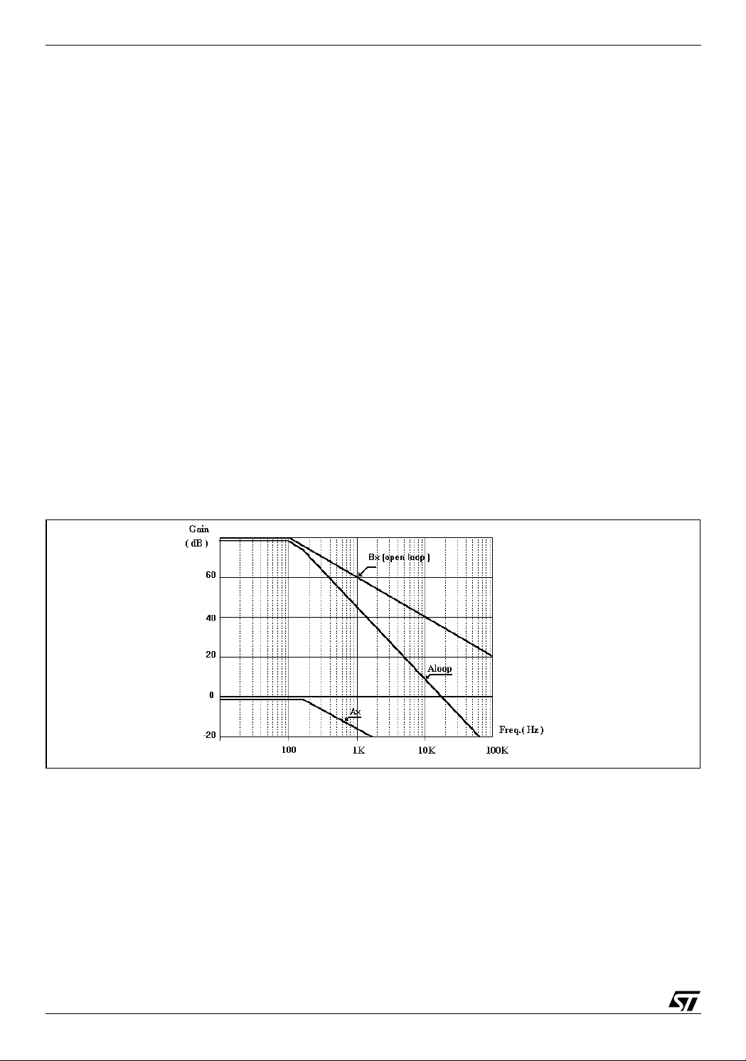
Figure 8.
The Bode plot of the Ax|dB function shows a DC gain of -1.9dB and a pole at 163Hz.
It is clear now that (because of the negative gain of the Ax function), Bx function must have an high DC gain in
13/24
Page 14
L6258E
order to increment the total open loop gain increasing the bandwidth too.
4.4 Error Amplifier and Sense Amplifier
As explained before the gain of these two blocks is :
Bx
= ACerrdB + ACsense
dB
Being the voltage across the sense resistor the input of the Bx block and the error amplifier voltage the output
of the same, the voltage gain is given by :
because ib = icwe have:
dB
ib Vsense Gs⋅ Vsense
Verr_out = -(ic · Zc) so ic = -(Verr_out · )
1
------- -
⋅==
Rb
1
------ -
Zc
1
Bx
------- -
Rb
Verr_out
------------------------–
Vsense
Vsense · = -(Verr_out · )
1
------ -
Zc
Zc
------- -–==
Rb
In the case of no external RC network is used to compensate the error amplifier, the typical open loop transfer
function of the error plus the sense amplifier is something with a gain around 80dB and a unity gain bandwidth
at 400kHz. In this case the situation of the total transfer function Aloop, given by the sum of the Ax
and Bx
dB
dB
is :
Figure 9.
The BODE diagram shows together the error amplifier open loop transfer function, the Ax function and the resultant total Aloop given by the following equation :
Aloop
= AxdB + Bx
dB
dB
The total Aloop has an high DC gain of 78.1dB with a bandwidth of 15KHz, but the problem in this case is the
stability of the system; in fact the total Aloop cross the zero dB axis with a slope of -40dB/decade.
Now it is necessary to compensate the error amplifier in order to obtain a total Aloop with an high DC gain and
a large bandwidth. Aloop must have enough phase margin to guarantee the stability of the system.
A method to reach the stability of the system, using the RC network showed in the block diagram, is to cancel
the load pole with the zero given by the compensation of the error amplifier.
14/24
Page 15

L6258E
The transfer function of the Bx block with the compensation on the error amplifier is :
1
------------------------ -
Rc j
Bx
Zc
------- -–
Rb
In this case the Bx block has a DC gain equal to the open loop and equal to zero at a frequency given by the
following formula:
---------------------------------------- -–==
–
2π fCc⋅⋅
Rb
Fzero
1
-------------------------------=
2π Rc Cc⋅⋅
In order to cancel the pole of the load, the zero of the Bx block must be located at the same frequency of 163Hz;
so now we have to find a compromise between the resistor and the capacitor of the compensation network.
Considering that the resistor value defines the gain of the Bx block at the zero frequency, it is clear that this
parameter will influence the total bandwidth of the system because, annulling the load pole with the error amplifier zero, the slope of the total transfer function is -20dB/decade.
So the resistor value must be chosen in order to have an error amplifier gain enough to guarantee a desired
total bandwidth .
In our example we fix at 35dB the gain of the Bx block at zero frequency, so from the formula:
Rc
------- -
log⋅=
Rb
where: Rb = 20k
Ω
we have: Rc = 1.1M
Bx_gain
@ zero freq.
20
Ω
Therefore we have the zero with a 163Hz the capacitor value :
Cc
---------------------------------------- -
2π Fzero Rc⋅⋅
1
------------------------------------------------------- 880pF== =
6.28 163 1.1 10
1
⋅⋅⋅
6–
Now we have to analyse how the new Aloop transfer function with a compensati on network on the error amplifier
is.
The following bode diagram shows :
– the Ax function showing the position of the load pole
– the open loop transfer function of the Bx block
– the transfer function of the Bx with the RC compensation network on the error amplifier
– the total Aloop transfer function that is the sum of the Ax function plus the transfer function of the com-
pensated Bx block.
15/24
Page 16

L6258E
Figure 10.
We can see that the effect of the load pole is cancelled by the zero of the Bx block ; the total Aloop cross a the
0dB axis with a slope of -20dB/decade, having in this way a stable system with an high gain at low frequency
and a bandwidth of around 8KHz.
To increase the bandwidth of the system, we should increase the gain of the Bx block, keeping the zero in the
same position. In this way the result is a shift of the total Aloop transfer function up to a greater value.
4.5 Effect of the Bemf of the stepper motor on the current control loop stability
In order to evaluate what is the effect of the Bemf voltage of the s tepper motor we have to look at the load block :
Figure 11.
OUT+
Bemf
R
L
L
L
R
S
OUT-
to Sense
Amplifier
The schematic now shows the equivalent circuit of the stepper motor including a sine wave voltage generator
of the Bemf. The Bemf voltage of the motor is not constant, its value changes depending on the speed of the
motor.
Increasing the motor speed the Bemf voltage increases :
Bemf = Kt ·
ω
where:
Kt is the motor constant
ω
is the motor speed in radiant per second
16/24
Page 17

L6258E
The formula defining the gain of the load considering the Bemf of the stepper motor becomes:
R
S
⋅
V
S
R
S
-------------------- -
⋅
RLRS+
-------------------- -
RLRS+
R
S
ACload
ACload
Vsense
--------------------- -
Acload
dB
Vout
20
Bemf–()
V
S
-----------------------------------------------------------==
V
Bemf–
S
----------------------------
V
S
V
----------------------------
log⋅=
S
⋅=
Bemf–
V
S
-------------------- -
RLRS+
we can see that the Bem f i nflu ences o nly the gain of the load block and does not intr oduce any other additi onal
pole or zero, so from the stability point of view the effect of the Bemf of the motor is not critical because the
phase margin remains the same.
Practically the only effect of the Bemf is to limit the gain of the total Aloop with a consequent variation of the
bandwidth of the system.
5 APPLICATION INFORMATION
A typical application circuit is shown in Fig.12.
Note: For avoid current spikes on falling edge of DISABLE a "DC feedback" would be added to the ERROR
Amplifier. (R1-R2 on Fig. 12).
5.1 Interference
Due to the fact that the circuit operates with switch mode current regulation, to reduce the effect of the wiring
inductance a good capacitor (100nF) c an be plac ed on the board near the package, between the power supply
line (pin 13,31) and the power ground (pin 1,36,18,19) to absorb the small amount of inductive energy.
It should be noted that this capacitor is usually required in addition to an electrolytic capacitor, that has poor
performance at the high frequencies, always located near the package, between power supply voltage (pin
13,31) and power ground (pin 1,36,18,19), just to have a current recircu lation path during the fast curren t decay
or during the phase change.
The range value of this capacitor is between few
µ
F and 100µF, and it must be chosen depending on application
parameters like the motor inductance and load current amplitude.
A decoupling capacitor of 100nF is suggested also between the logic supply and ground.
The EA_IN1 and EA_IN2 pins carry out high impedance lines and care must be taken to avoid coupled noise
on this signals. The suggestion is to put the components c onnected to this pins close to the L6258E, to surround
them with ground tracks and to keep as far as possible fast switching outputs of the devi ce. Remember als o an
1 Mohm resistor between EA_INx and EA_OUTx to avoid out put current spi ke during supply startup/shutdo wn.
A non inductive resistor is the best way to implement the sens ing. Whether this is not possi ble, some metal f ilm
resistor of the same value can be paralleled.
The two inputs for the sensing of the winding motor current (SENSE_A & SENSE_B) should be connected directly on the sensing resis tor Rs terminals , and the pa th lead between the Rs and the two sens ing inputs shoul d
be as short as possible.
17/24
Page 18

L6258E
Figure 12. Typical Application Circuit.
VS
10nF
100nF
1nF
VCP1
VCP2
VBOOT
TRI_CAP
I0_1
I1_1
I2_1
I3_1
PH2
I0_2
I1_2
I2_2
I3_2
DISABLE
VS
EA_IN1
10
11
12
13,31
7
2
4
3
32
33
17
15
16
23
22
6
OUT2B
SENSE2
OUT2A
SENSE1
OUT1B
OUT1APH1
GND
PWR_GND
V
DD
SIG_GND
VREF1
VREF2
0.33
0.33
D97IN626E
M
VDD(5V)
VREF
STEPPER
MOTOR
12mH 10Ω
21
20
14
35
34
L6258
SOP36
E
5
9
PACKAGE
1,36
18,19
8
27
28
26
29
EA_OUT1
1M
820pF
30
EA_IN2
25
EA_OUT2
1M
R2 1MR1 1M
24
820pF
5.2 Motor Selection
Some stepper motor have such high core losses that they are not suitable for switch mode current regulation. Furthermore, some stepper motors are not designed for continuous operating at maximum current. Since the circuit
can drive a c onstant current t hrough th e motor, i ts temperat ure might exceed, both at lo w and high speed ope ration.
5.3 Unused Inputs
Unused inputs should be connected to the proper voltage levels in order to get the highest noise immunity.
5.4 Notes on PCB Design
We recommend to observe the foll owing lay out rule s to avoi d application problem s with gr ound and anoma lous
recirculation current.
The by-pass capacitors for the power and logic supply must be kept as near as possible to the IC.
It's important to separate on the PCB board the logic and power grounds and the internal charge pump circuit
ground avoiding that ground traces of the logic signals cross the ground traces of the power signals.
Because the IC uses the board as a heat sink, the di ssipating c opper area must be sized in accordance with th e
required value of R
thj-amb
.
18/24
Page 19

L6258E
6 OPERATION MODE TIME DIAGRAMS
Figure 13. Full step operation mode timing diagram (Phase - DAC input and Motor Current)
Position
Phase
1
Phase
2
DAC 1
Inputs
DAC 2
Inputs
Motor drive
Current 1
Motor drive
Current 2
I0_1
I1_1
I2_1
I3_1
I0_2
I1_2
I2_2
I3_2
5V
0
5V
0
5V
0
5V
0
5V
0
5V
0
5V
0
5V
0
5V
0
0
0
0
023103210
Ph2
95.2%
19.1%
95.2%
19.1%
D97IN629A
FULL Step Vector
Ph1
1
Ph1
0
Ph2
32
I3 I2 I1 I0
Current level
% of I
MAX
0000 100
0001 98.4
0010 95.2
0011 92.1
0100 88.9
0101 82.5
0110 77.8
0111 71.4
1000 63.5
1001 55.6
1010 47.6
1011 38.1
1100 28.6
1101 19.1
1110 9.5
1111 No Current
19/24
Page 20
L6258E
Figure 14. Half step operation mode timing diagram (Phase - DAC input and Motor Current)
67451320
I0_1
I1_1
I2_1
I3_1
I0_2
I1_2
I2_2
I3_2
5V
0
5V
0
5V
0
5V
0
5V
0
5V
0
5V
0
5V
0
5V
0
5V
0
100%
71.4%
0
-71.4%
-100%
100%
71.4%
0
-71.4%
-100%
Ph2
D97IN627C
Half Step Vector
Ph1
2
of I
1
7
MAX
3
4
5
6
Ph1
I3 I2 I1 I0
0000 100
0001 98.4
0010 95.2
0011 92.1
0100 88.9
0101 82.5
0110 77.8
0111 71.4
1000 63.5
1001 55.6
1010 47.6
1011 38.1
1100 28.6
1101 19.1
1110 9.5
1111 No Current
Current level%
0
Phase 1
Phase 2
DAC 1
Inputs
DAC 2
Inputs
Motor drive
Current 1
Motor drive
Current 2
Ph2
20/24
Page 21

L6258E
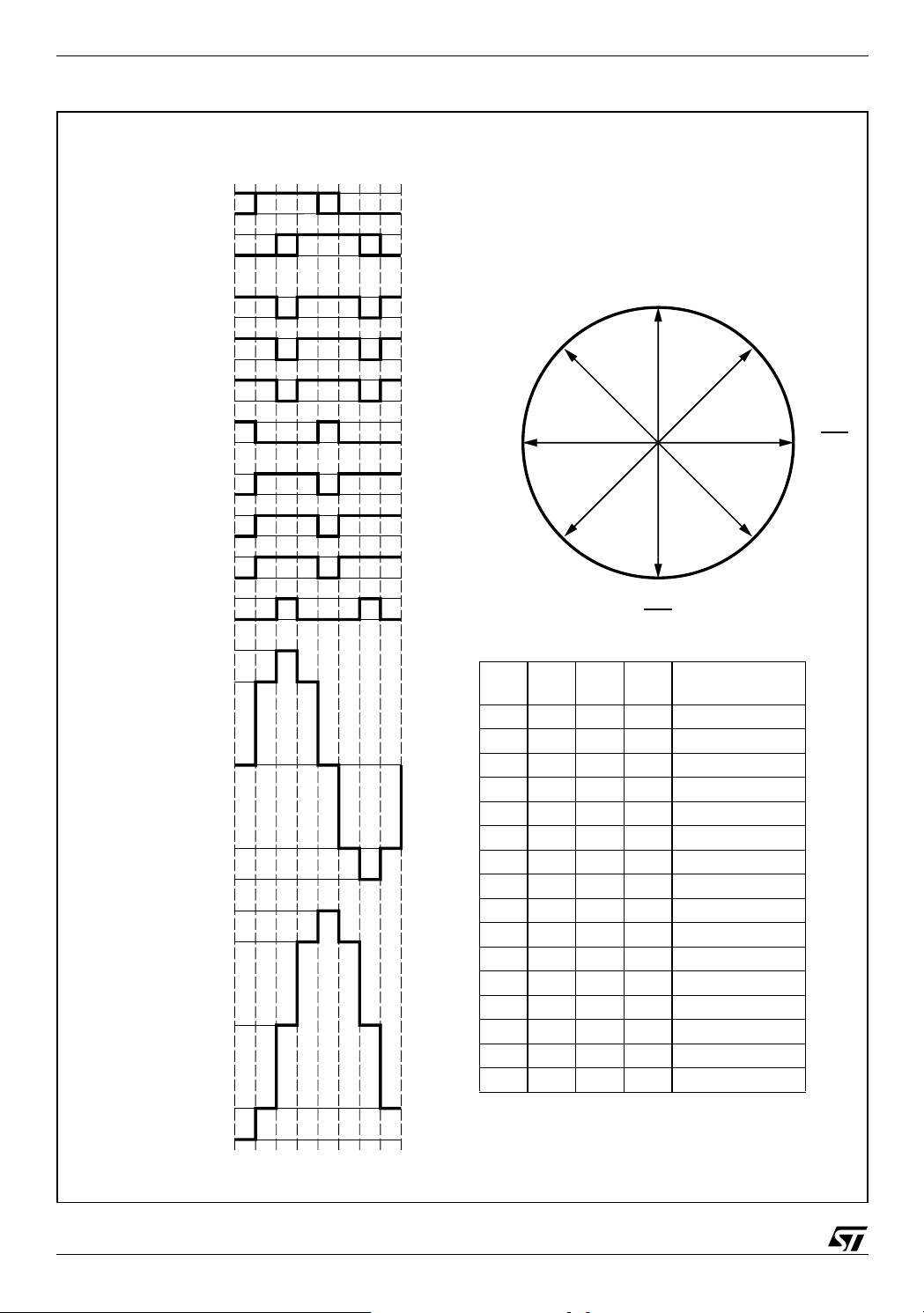
Figure 15. 4 bit microstep operation mode timing diagram (Phase - DAC input and Motor Current)
Position
Phase
1
Phase
2
I0_1
I1_1
DAC 1
Inputs
I2_1
I3_1
I0_2
DAC 2
Inputs
I1_2
I2_2
I3_2
Motor drive
Current 1
Motor drive
Current 2
5V
5V
5V
5V
5V
5V
5V
5V
5V
0
4
8
12
16
20
36
40
44
48
52
24
28
32
56
60
64
Micro Step Vector
Ph1
0
24
0
Ph2
0
0
0
32
40
16
8
0
Ph2
56
48
Ph1
0
0
0
I3 I2 I1 I0
Current level%
of I
MAX
0000 100
0001 98.4
0
0010 95.2
0011 92.1
0
100%
95.2%
82.5%
63.5%
47.6%
38.1%
19.1%
0
0%
0100 88.9
0101 82.5
0110 77.8
0111 71.4
1000 63.5
1001 55.6
1010 47.6
1011 38.1
1100 28.6
1101 19.1
0
1110 9.5
1111 No Current
D97IN628A
21/24
Page 22

L6258E
Figure 16. PowerSO36 Mechanical Data & Package Dimensions
DIM.
mm inch
MIN. TYP. MAX. MIN. TYP. MAX.
A 3.25 3.5 0.128 0.138
A2 3.3 0.13
A4 0.8 1 0.031 0.039
A5 0.2 0.008
a100.07500.003
b 0.22 0.38 0.008 0.015
c 0.23 0.32 0.009 0.012
D 15.8 16 0.622 0.630
D1 9.4 9.8 0.37 0.38
D2 1 0.039
E 13.9 14.5 0.547 0.57
E1 10.9 11.1 0.429 0.437
E2 2.9 0.114
E3 5.8 6.2 0.228 0.244
E4 2.9 3.2 0.114 1.259
e 0.65 0.026
e3 11.05 0.435
G 0 0.075 0 0.003
H 15.5 15.9 0.61 0.625
h 1.1 0.043
L 0.8 1.1 0.031 0.043
N 10˚ (max)
s 8˚ (max)
Note: “D a nd E 1” do not include mold flash or protusions.
- Mold flash or protusions sh al l not exceed 0.15mm (0.006”)
- Critical dimensions are "a3", "E" and "G " .
OUTLINE AND
MECHANICAL DA T A
PowerSO36
E2
NN
DETAIL A
118
h x 45
A
e3
H
D
1936
b
0.12 AB
a2
A
e
M
E1
DETAIL B
lead
a3
B
Gage Plane
PSO36MEC
BOTTOM VIEW
DETAIL B
0.35
S
L
DETAIL A
a1
E
slug
D1
SEATING PLANE
(COPLANARITY)
c
E3
- C -
GC
0096119 B
22/24
Page 23

Table 8. Revision History
Date Revi sio n Description of Chan g es
January 2004 5 First Issue in EDOCS DMS
L6258E
May 2004 6 Restyling of the graphic form, changed all V
delete TSD parameter in the Electrical characteristic on the page 5/24.
NOT FOR NEW DESIGN, it has been replaced by equivalent L6258EX.
September 2004 7 Changed on the page 5 the f
18.5kHz
parameter max. value from 17.5 to
osc
with VDD;
CC
23/24
Page 24

L6258E
Information furnished is believed to be accurate and reliable. However, STMicroelectronics assumes no responsibility for the consequences
of use of such information nor for any infri ngement of patents or other rights of third parties which may result from its use. No licens e is granted
by implication or otherwise under any patent or patent rights of STMicroelectronics. Specifications mentioned in this publication are subject
to change without no tice. This publication supersedes and replaces all information previously supplied. STMicroelectronics products are not
authorized for use as critical components in life support devices or systems without express written approval of STMicroelectronics.
The ST logo is a registered trademark of STMicroelectronics.
All other names are the property of their respective owners
© 2004 STMicroelectronics - All rights reserved
Australia - Belgium - Brazil - Canada - China - Czec h Republic - Finland - France - Germany - Hong Kong - India - Is rael - Italy - Japan -
Malaysia - Malta - Morocco - Singapore - Spain - Sweden - Switzerland - United Kingdom - United States of America
STMicroelectronics group of companies
www.st.com
24/24
 Loading...