

Page 1
HEX BUFFER/CONVERTER (INVERTING)
■ PROPAGATION DELAY TIME:
t
= 40ns (TYP.) at VDD= 10V CL= 50pF
PD
■ HIGH TO LOW LEVEL LOGIC CONVERSION
■ HIGH "SINK" AND "SOURCE" CURRENT
CAPABILITY
■ QUIESCENT CURRENT SPECIFIED UP TO
20V
■ 5V,10V AND 15V PARAMETRIC RATINGS
■ INPUT LEAKAGE CURRE NT
I
= 100nA (MAX) AT VDD=18VTA= 25°C
I
■ 100% TESTED FOR QUIESCENT CURRENT
DESCRIPTION
The HCF4049UB is a monolithic integrated circuit
fabricated in Metal Oxide Semiconductor
technology available in DIP and SOP packages.
It is an in ve rting Hex Buffer/Converter and feature
logic level conversions using only one supply
voltage (V
The input high level signal (V
V
supply voltage when t hes e devices are used
DD
DD
).
) can exceed the
IH
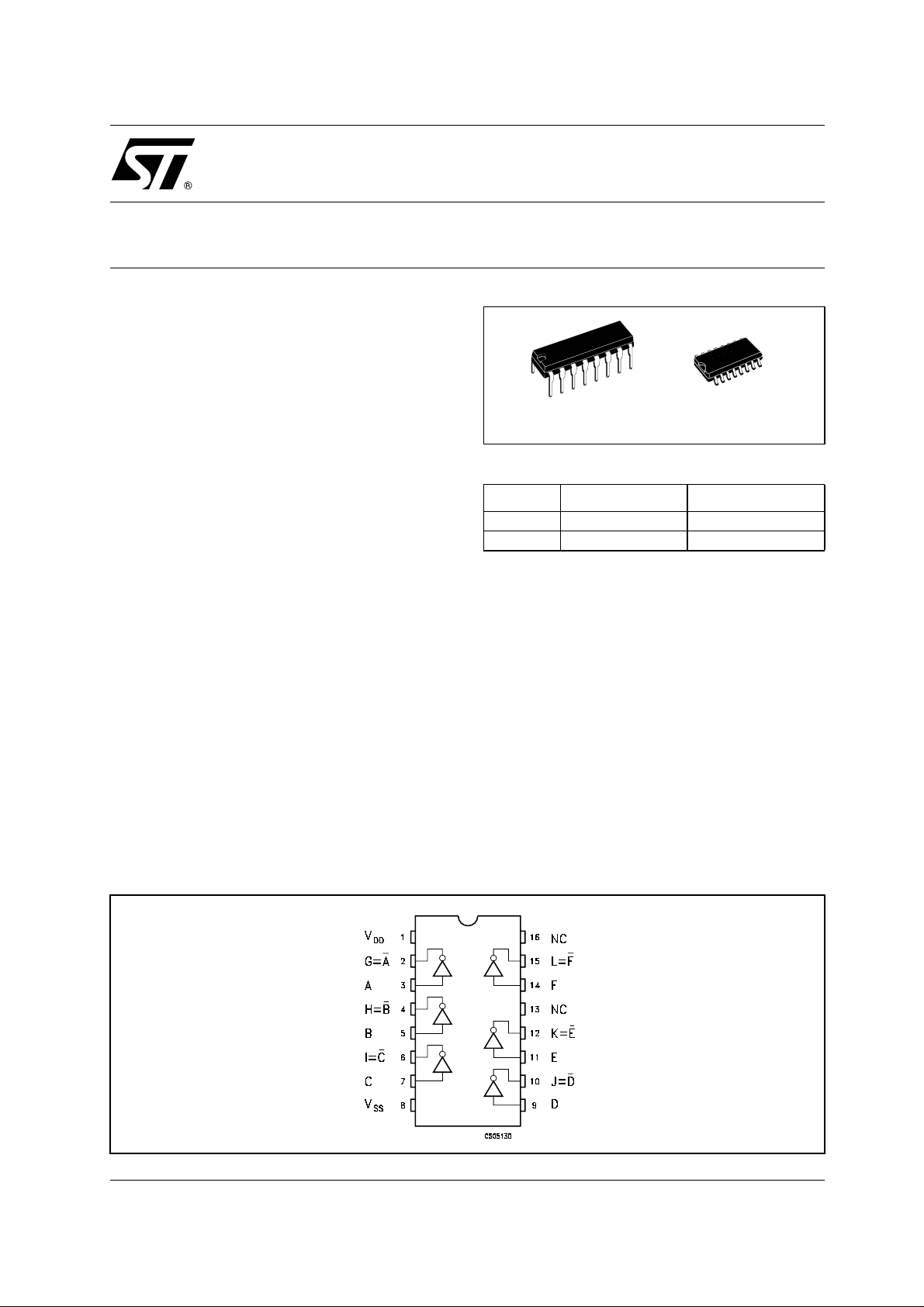
HCF4049UB
DIP SOP
ORDER CODES
PACKAGE TUBE T & R
DIP HCF4049UBEY
SOP HCF4049UBM1 HCF4049UM013TR
for logic level conversions. This device is intended
for use as CMOS to DTL/TTL converters and can
drive directly two DTL/TTL loads (V
0.4V and I
≤ 3.2mA.
OL
=5V,V
DD
OL
≤
PIN CONNECTION
1/9March 2004
Page 2
HCF4049UB
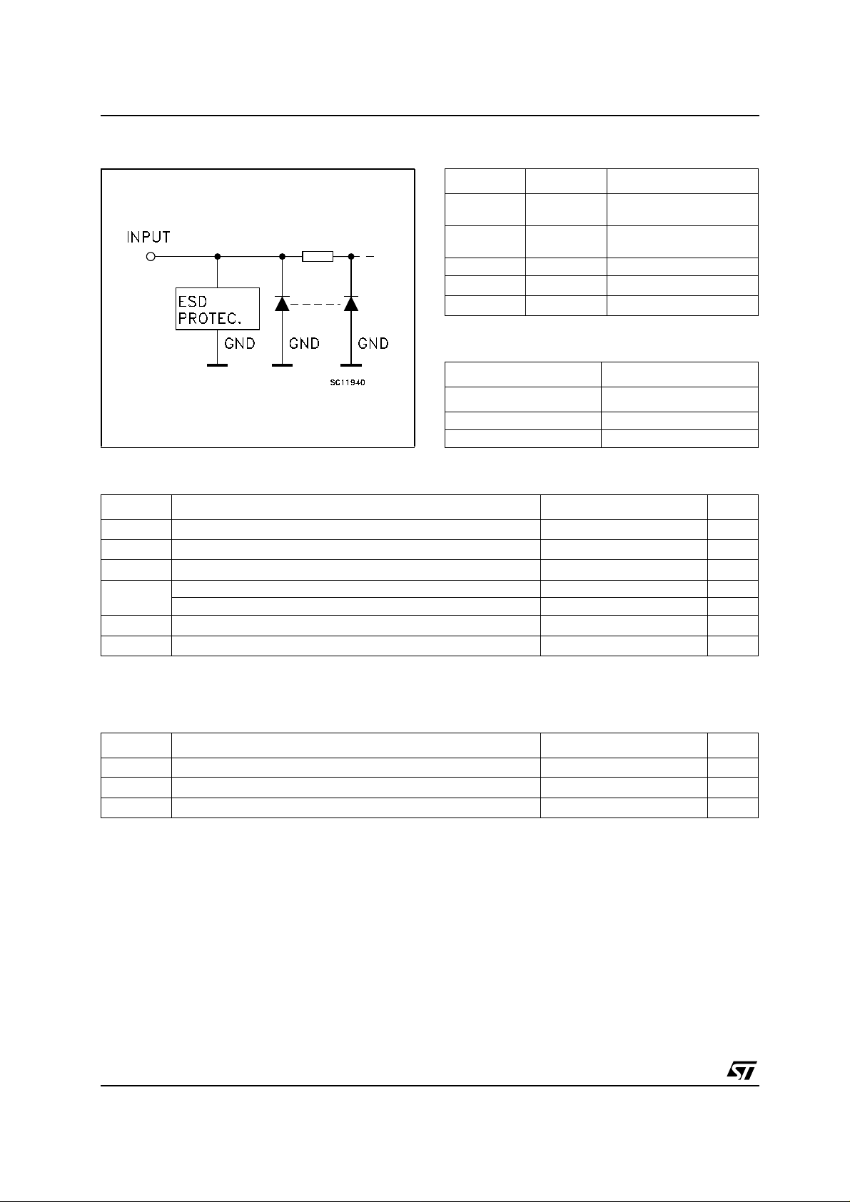
INPUT EQUIVALENT CIRCUIT PIN DESCRIP TION
PIN N° SYMBOL NAME AND FUNCTION
3, 5, 7, 9, 11,14A, B,C, D,E,
F
2, 4, 6, 10,
12, 15
G, H, I, J, K,
L
13, 16 NC Not Connected
8
1
V
SS
V
DD
TRUTH TABLE
INPUTS OUTPUTS
A,B,C,D,E,F G,H,I,J,K,L
LH
HL
ABSOLUTE MAXIMUM RATINGS
Symbol Parameter Value Unit
V
V
P
T
T
stg
Absolute Maximum Ratings are those values beyond which damage to the device may occur. Functional operation under these conditions is
not implied.
All voltagevalues are referred to VSSpin voltage.
Supply Voltage
DD
DC Input Voltage
I
DC Input Current
I
I
Power Dissipation per Package 200 mW
D
Power Dissipation per Output Transistor 100 mW
Operating Temperature
op
Storage Temperature
Data Inputs
Data Outputs
Negative Supply Voltage
Positive Supply Voltage
-0.5 to +22 V
-0.5 to +18 V
± 10 mA
-55 to +125 °C
-65 to +150 °C
RECOMMENDED OPERATING CONDITIONS
Symbol Parameter Value Unit
V
V
T
2/9
Supply Voltage
DD
Input Voltage -0.5 to 15V
I
Operating Temperature
op
3to20 V
-55 to 125 °C
V
Page 3
DC SPECIFICATIONS
Test Condition Value
T
Symbol Parameter
I
Quiescent Current 0/5 5 0.02 1 30 30
L
V
(V)
V
I
(V)
|I
|
O
O
(µA)
V
DD
(V)
= 25°C
A
Min. Typ. Max. Min. Max. Min. Max.
0/10 10 0.02 2 60 60
0/15 15 0.02 4 120 120
0/20 20 0.04 20 600 600
V
High Level Output
OH
Voltage
0/5 <1 5 4.95 4.95 4.95
0/15 <1 15 14.95 14.95 14.95
V
Low Level Output
OL
Voltage
5/0 <1 5 0.05 0.05 0.05
15/0 <1 15 0.05 0.05 0.05
V
High Level Input
IH
Voltage
0.5/4.5 <1 5 4 4 4
1.5/13.5 <1 15 12 12 12
V
Low Level Input
IL
Voltage
4.5/0.5 <1 5 1 1 1
13.5/1.5 <1 15 3 3 3
I
OH
Output Drive
Current
0/5 2.5 <1 5 -1.25 -6.4 -0.42 -0.42
0/5 4.6 <1 5 -0.51 -1.6 -0.38 -0.38
0/10 9.5 <1 10 -1.25 -3.6 -1 -1
0/15 13.5 <1 15 -3.75 -12 -3 -3
I
OL
Output Sink
Current
0/5 0.4 <1 5 3.2 6.4 2.6 2.6
0/15 1.5 <1 15 24 48 19 19
I
Input Leakage
I
Current
Input Capacitance
C
I
The Noise Margin forboth "1"and "0" level is:1V min. with VDD=5V, 2V min. with VDD=10V, 2.5V min. with VDD=15V
0/18 Any Input 18
Any Input 5 7.5 pF
±10
-5
-40 to 85°C -55 to 125°C
±0.1 ±1 ±1 µA
HCF4049UB
Unit
µA
V0/10 <1 10 9.95 9.95 9.95
V10/0 <1 10 0.05 0.05 0.05
V1/9 <1 10 8 8 8
V9/1 <1 10 2 2 2
mA
mA0/10 0.5 <1 10 8 16 6.6 6.6
3/9
Page 4

HCF4049UB
DYNAMIC ELECTRICAL CH ARACTERISTICS (T
Symbol Parameter
t
t
t
t
(*) Typical temperature coefficient for all VDDvalue is 0.3%/°C.
Output Transition Time 5 5 80 160
TLH
Output Transition Time 5 5 30 60
THL
Propagation DelayTime 5 5 60 120
PLH
Propagation DelayTime 5 5 32 65
PHL
(V) VI(V)
V
DD
15 15 30 60
15 15 15 30
10 10 32 65
510 4590
15 15 25 50
515 4590
10 10 20 40
510 1530
15 15 15 30
515 1020
TEST CIRCUIT
=25°C,CL= 50pF, RL= 200KΩ,tr=tf=20ns)
amb
Test Condition Value (*) Unit
Min. Typ. Max.
ns10 10 40 80
ns10 10 20 40
ns
ns
CL= 50pF or equivalent (includes jig and probe capacitance)
R
=200KΩ
L
R
T=ZOUT
of pulse generator (typically 50Ω)
4/9
Page 5

WAVEFORM: PROPAGATION DELAY TIMES (f=1MHz; 50% duty cycle)
HCF4049UB
5/9
Page 6

HCF4049UB
Plastic DIP-16 (0.25) MECHANICAL DATA
mm. inch
DIM.
MIN. TYP MAX. MIN. TYP. MAX.
a1 0.51 0.020
B 0.77 1.65 0.030 0.065
b 0.5 0.020
b1 0.25 0.010
D 20 0.787
E 8.5 0.335
e 2.54 0.100
e3 17.78 0.700
F 7.1 0.280
I 5.1 0.201
L 3.3 0.130
Z 1.27 0.050
6/9
P001C
Page 7

SO-16 MECHANICAL DATA
HCF4049UB
DIM.
A 1.75 0.068
a1 0.1 0.2 0.004 0.008
a2 1.65 0.064
b 0.35 0.46 0.013 0.018
b1 0.19 0.25 0.007 0.010
C 0.5 0.019
c1 45˚ (typ.)
D 9.8 10 0.385 0.393
E 5.8 6.2 0.228 0.244
e 1.27 0.050
e3 8.89 0.350
F 3.8 4.0 0.149 0.157
G 4.6 5.3 0.181 0.208
L 0.5 1.27 0.019 0.050
M 0.62 0.024
S8 ˚ (max.)
MIN. TYP MAX. MIN. TYP. MAX.
mm. inch
PO13H
7/9
Page 8

HCF4049UB
Tape & Reel SO-16 MECHANICAL DATA
mm. inch
DIM.
MIN. TYP MAX. MIN. TYP. MAX.
A 330 12.992
C 12.8 13.2 0.504 0.519
D 20.2 0.795
N 60 2.362
T 22.4 0.882
Ao 6.45 6.65 0.254 0.262
Bo 10.3 10.5 0.406 0.414
Ko 2.1 2.3 0.082 0.090
Po 3.9 4.1 0.153 0.161
P 7.9 8.1 0.311 0.319
8/9
Page 9

HCF4049UB
Information furnished is believed to be accurate and reliable. However, STMicroelectronics assumes no responsibility for the
consequences of use of such inform ation nor fo r an y infring ement of p atents or o ther rights of third p arties which may r esult f rom
its use. No license is granted by implication or otherwise under any patent or patent rights of STMicroelectronics. Specifications
mentioned in this publication are subject to change without notice. This publication supersedes and replaces all information
previously supplied. STMicroelectronics products are not authorized for use as critical components in life support devices or
systems without express written approval of STMicroelectronics.
Australia - Belgium - Brazil - Canada - China - Czech Republic - Finland - France - Germany - Hong Kong - India - Israel - Italy - Japan -
Malaysia - Malta - Morocco - Singapore - Spain - Sweden - Switzerland - United Kingdom - United States.
The ST logo is a registered trademark of STMicroelectronics
All other names are the property of their respective owners
© 2004 STMicroelectronics - All Rights Reserved
STMicroelectronics GROUP OF COMPANIES
http://www.st.com
9/9
 Loading...