

Page 1

HCF40107B
DUAL 2-INPUT NAND BUFFER/DRIVER
■ 32 TIMES STANDARD B-SERIES OUTPUT
CURRENT DRIVE SINKING CAPABILITY 136 mA TYP. AT V
■ QUIESCENT CURRENT SPECIF . UP TO 20V
■ 5V , 10V AND 15V PARAMETRIC RATINGS
■ INPUT LEAKAGE CURRENT
I
= 100nA (MAX) AT VDD = 18V TA = 25°C
I
■ 100% TESTED FOR QUIESCENT CURRENT
■ MEETS ALL REQUIREMENTS OF JEDEC
= 10V, VDS = 1V
DD
JESD13B "STANDARD SPECIFICATIONS
FOR DESCRIPTI ON OF B SERI ES CMOS
DEVICES"
DESCRIPTION
HCF40107B is a monolithic integrated circuit
fabricated in Metal Oxide Semiconductor
technology available in DIP and SOP packages.
HCF40107B is a dual 2-input NAND buffer/driver
containing two independent 2-input NA ND buffers
with open-drain single n-channel transistor
outputs. This device features a wired-OR
capability and hig h output sink current capa bility
(136 mA typ. at V
= 10V, VDS = 1V).
DD
DIP SOP
ORDER CODES
PACKAGE TUBE T & R
DIP HCF40107BEY
SOP HCF40107BM1 HCF40107M013TR
PIN CONNECTION
1/11October 2002
Page 2

HCF40107B
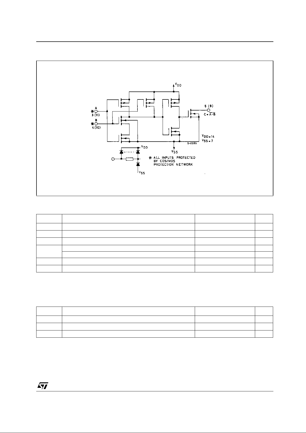
INPUT EQUIVALENT CIRCUIT PIN DESCRIPTION
PIN No SYMBOL NAME AND FUNCTION
2, 1, 7, 6 A, B, D, E Input
3, 5 C,F Outputs
4
8
FUNCTIONAL DIAGRAM
V
SS
V
DD
Negative Supply Voltage
Positive Supply Voltage
TRUTH TABLE
AB C
LLH*
HLH*
LHH*
HHL
* : Requires external and pull-up resistor (RL) to VDD.
# : Without pull-up resistor (3-state).
2/11
#
Z
#
Z
#
Z
Page 3
LOGIC DIAGRAM
HCF40107B
ABSOLUTE MAXIMUM RATINGS
Symbol Parameter Value Unit
V
V
P
Supply Voltage
DD
DC Input Voltage -0.5 to VDD + 0.5
I
I
DC Input Current
I
Power Dissipation per Package 200 mW
D
-0.5 to +22 V
10 mA
±
V
Power Dissipation per Output Transistor 100 mW
T
T
Absolute Maximum Ratings are those values beyond which damage to the device may occur. Functional operation under these conditions is
not implied.
All voltage values are referred to V
Operating Temperature
op
Storage Temperature
stg
pin voltage.
SS
-55 to +125 °C
-65 to +150 °C
RECOMMENDED OPERATING CONDITIONS
Symbol Parameter Value Unit
V
V
T
Supply Voltage
DD
Input Voltage 0 to V
I
Operating Temperature
op
3 to 20 V
DD
-55 to 125 °C
V
3/11
Page 4
HCF40107B
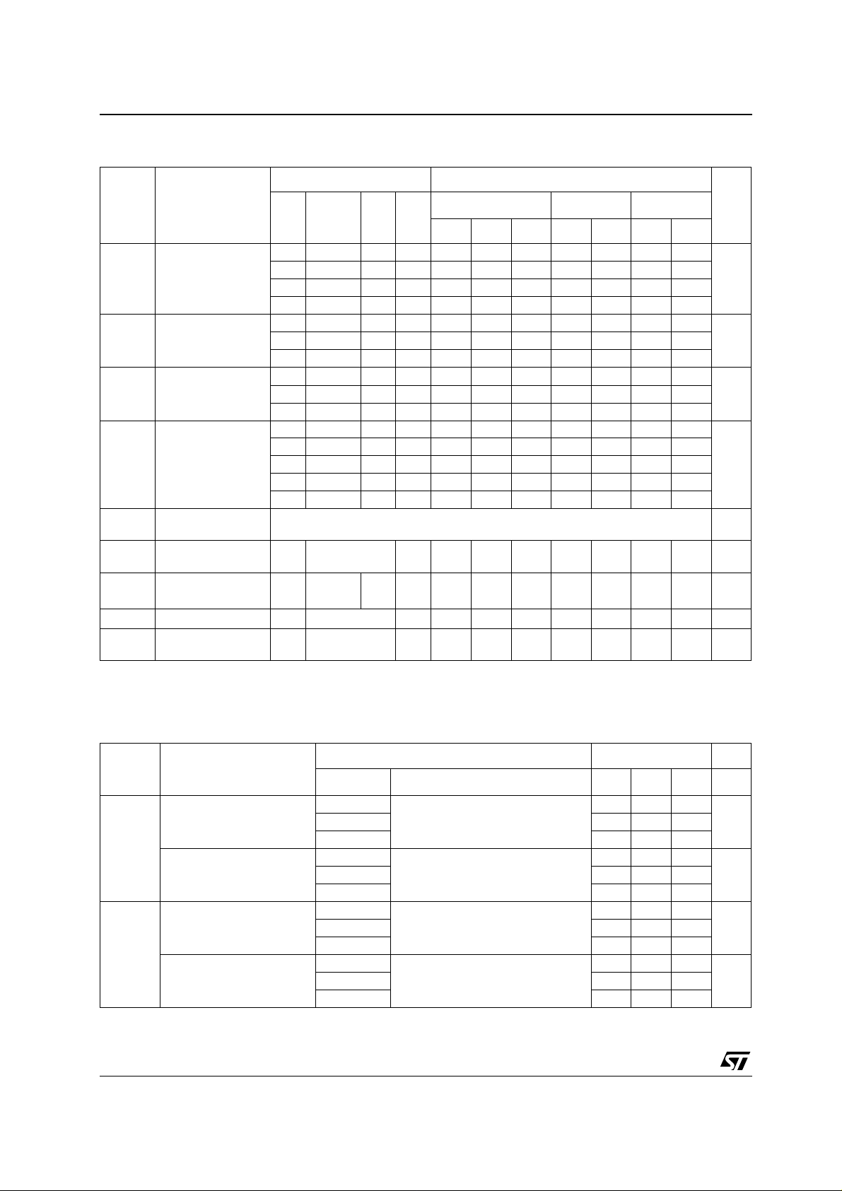
DC SPECIFICATIONS
Test Condition Value
T
Symbol Parameter
I
Quiescent Current 0/5 5 0.02 5 150 30
L
V
(V)
V
I
(V)
|I
|
O
O
(µA)
V
DD
(V)
= 25°C
A
Min. Typ. Max. Min. Max. Min. Max.
0/10 10 0.02 10 300 60
0/15 15 0.02 20 600 120
0/20 20 0.04 100 3000 600
V
High Level Input
IH**
Voltage
0.5/4.5 <1 5 3.5 3.5 3.5
1.5/13.5 <1 15 11 11 11
V
Low Level Input
IL**
Voltage
4.5/0.5 <1 5 1.5 1.5 1.5
13.5/1.5 <1 15 4 4 4
I
OL
Output Sink
Current
5 0.4 5 21 32 16 12
51 54468 30 25
10 0.5 10 49 74 37 28
10 1 10 89 136 68 51
15 0.5 15 66 100 50 38
Output Drive
I
OH
Current
I
IH, IIL
I
OH, IOL
The Noi se Margin fo r both "1" and "0" level is: 1V min. with VDD=5V, 2V min. with VDD=10V, 2.5V min. with VDD=15V
** Measur e d wi th exter nal pull-up resistor, R
*** Forced output dis abled.
Input Leakage
Current
3-State Output
Leakage Current
***
C
Input Capacitance
I
C
Output
O
Capacitance
0/18 Any Input 18
0/18 18 18
Any Input 5 7.5 pF
Any Output 30 pF
= 10kΩ to VDD.
L
No Internal Pull-up Device mA
-5
10
±
-4
10
±
-40 to 85°C -55 to 125°C
0.1
±
0.1
±
2220
1
±
Unit
A
µ
V1/9 <1 10 7 7 7
V9/1 <1 10 3 3 3
mA
A
µ
A
µ
DYNAMIC ELECTRICAL CHARACTERISTICS (T
Symbol Parameter
t
PHL tPLH
Propagation Delay Time
High to Low
Low to High 5
t
THL tTLH
Transition Time
High to Low
Low to High 5
(*) RL is external pull-up resistor to V
4/11
DD.
(V)
V
DD
5
15 30 60
15 50 100
5
15 10 20
15 25 50
= 25°C, CL = 50pF, RL = 200KΩ, tr = tf = 20 ns)
amb
Test Condition Value (*) Unit
Min. Typ. Max.
100 200
R
* = 120
L
Ω
ns10 45 90
100 200
* = 120
R
L
Ω
ns10 60 120
50 100
R
* = 120
L
Ω
ns10 20 40
50 100
* = 120
R
L
Ω
ns10 35 70
Page 5

TYPICAL APPLICATIONS
HCF40107B
Line-driver Circuit.
Interface of 40107B with Triac, with COS/MOS
Component and Triac isolated.
A 2.2-watt Incandescent Lamp-driver Circuit.
Solenoid Driver Circuit
Direct Dc Driver Interface of 40107B with a Triac.
5/11
Page 6

HCF40107B
Multiplexed Led Circuit
6/11
Page 7

Motor-controller Circuit Led Driver Circuit
A B MOTOR FUNCTION
LL OFF
H L COUNTER CLOCKWISE
H H AS PREVIOUS STATE
L H CLOCKWISE
H H AS PREVIOUS STATE
INHIBIT ENABLE OUTPUT
L L OFF
H L OFF
L H OFF
LHON
HCF40107B
TEST CIRCUIT
CL = 50pF or equivalent (in cludes jig and probe capac i t ance)
R
= 200K
Ω
L
R
= Z
of pulse generator (typically 50Ω)
T
OUT
7/11
Page 8

HCF40107B
WAVEFORM : PROPAGATION DELAY TIMES (f=1MHz; 50% duty cycle)
8/11
Page 9

Plastic DIP-8 MECHANICAL DATA
HCF40107B
DIM.
MIN. TYP MAX. MIN. TYP. MAX.
A 3.3 0.130
a1 0.7 0.028
B 1.39 1.65 0.055 0.065
B1 0.91 1.04 0.036 0.041
b 0.5 0.020
b1 0.38 0.5 0.015 0.020
D 9.8 0.386
E 8.8 0.346
e 2.54 0.100
e3 7.62 0.300
e4 7.62 0.300
F 7.1 0.280
I 4.8 0.189
L 3.3 0.130
Z 0.44 1.6 0.017 0.063
mm. inch
P001F
9/11
Page 10

HCF40107B
SO-8 MECHANICAL DATA
DIM.
A 1.75 0.068
a1 0.1 0.25 0.003 0.009
a2 1.65 0.064
a3 0.65 0.85 0.025 0.033
b 0.35 0.48 0.013 0.018
b1 0.19 0.25 0.007 0.010
C 0.25 0.5 0.010 0.019
c1 45˚ (typ.)
D 4.8 5.0 0.189 0.196
E 5.8 6.2 0.228 0.244
e 1.27 0.050
e3 3.81 0.150
F 3.8 4.0 0.149 0. 157
L 0.4 1.27 0.015 0.050
M 0.6 0.023
S
MIN. TYP MAX. MIN. TYP. MAX.
mm. inch
˚ (max.)
8
10/11
0016023
Page 11

HCF40107B
Information furnished is believed to be accurate and reliable. However, STMicroelectronics assumes no responsibilit y for t he
consequences of use of such informatio n nor for any infringement of paten ts or o ther rig hts of t hird part ies which ma y result from
its use. No license is granted by implication or otherwise under any patent or patent rights of STMicroelectronics. Specifications
mentioned in this publication are subject to change without notice. This publication supersedes and replaces all information
previousl y suppl ied. STM icroel ectronics produc ts are not auth orized for use as c ritica l compone nts in l ife s upport dev ices or
systems without express written approval of STMicroelectronics.
Australia - Brazil - Canada - China - Finland - France - Germany - Hong Kong - India - Israel - Italy - Japan - Malaysia - Malta - Morocco
© The ST logo is a registered trademark of STMicroelectronics
© 2002 STMicroelectronics - Printed in Italy - All Rights Reserved
STMicroelectronics GROUP OF COMPANIES
Singapore - Spain - Sweden - Switzerland - United Kingdom - United States.
© http://www.st.com
11/11
 Loading...