

Features
Obsolete Product(s) - Obsolete Product(s)
rd
■ 3
order high resolution sigma delta converter
for MPX sampling
■ Digital decimation and filtering stages
■ Demodulation of european radio data system
(RDS)
■ Demodulation of USA radio broadcast data
system (RBDS)
■ Automatic group and block synchronization
with flywheel mechanism
■ Error detection and correction
■ RAM buffer with a storage capacity of 24 RDS
blocks and related status information
■ Programmable interrupt source (RDS block
TA)
2
■ I
C/SPI bus interface
■ Common quartz frequency 8.55 MHz or
8.664 MHz
■ 3.3 V power supply, 0.35 µm CMOS
technology
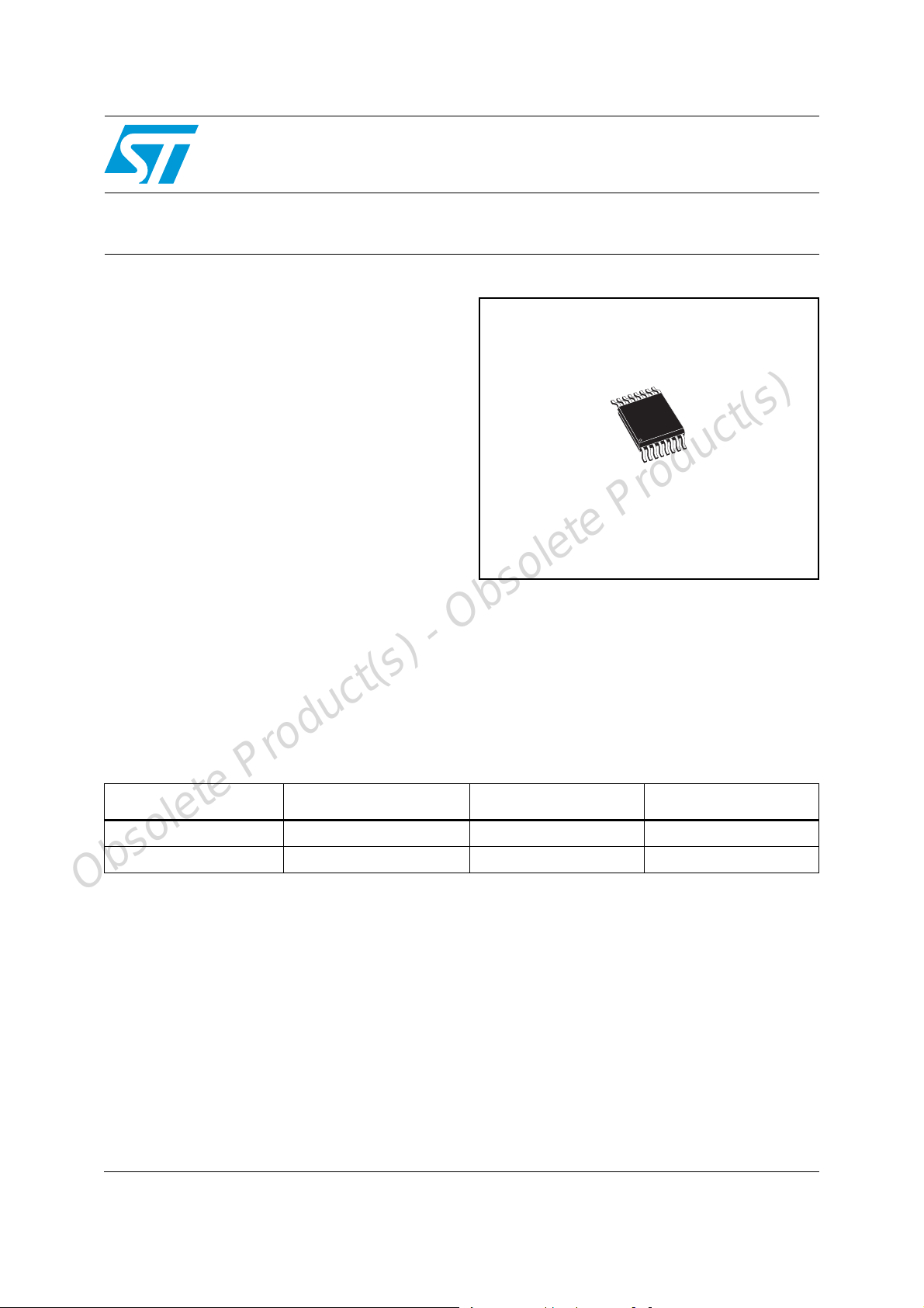
TDA7333
RDS/RBDS processor
TSSOP16
Description
The TDA7333 circuit is a RDS/RDBS signal
processor, intended for recovering the inaudible
RDS/RBDS informations which are transmitted on
most FM radio broadcasting stations.
Table 1. Device summary
Order code
E-TDA7333 -40 to +85 TSSOP16 Tube
E-TDA7333013TR -40 to +85 TSSOP16 Tape and reel
1. Devices in ECOPACK® package (see Section 5: Package information).
(1)
Operating temp. range, °C Package Packing
Obsolete Product(s) - Obsolete Product(s)
June 2008 Rev 1 1/26
www.st.com
1

Obsolete Product(s) - Obsolete Product(s)
Contents TDA7333
Contents
1 Block diagram and pin description . . . . . . . . . . . . . . . . . . . . . . . . . . . . . 5
1.1 Block diagram . . . . . . . . . . . . . . . . . . . . . . . . . . . . . . . . . . . . . . . . . . . . . . . 5
1.2 Pin description . . . . . . . . . . . . . . . . . . . . . . . . . . . . . . . . . . . . . . . . . . . . . . 5
2 Electrical specifications . . . . . . . . . . . . . . . . . . . . . . . . . . . . . . . . . . . . . . 7
2.1 Quick reference . . . . . . . . . . . . . . . . . . . . . . . . . . . . . . . . . . . . . . . . . . . . . 7
2.2 Absolute maximum ratings . . . . . . . . . . . . . . . . . . . . . . . . . . . . . . . . . . . . . 7
2.3 General interface electrical characteristics . . . . . . . . . . . . . . . . . . . . . . . . . 7
2.4 Electrical characteristics . . . . . . . . . . . . . . . . . . . . . . . . . . . . . . . . . . . . . . . 8
3 Functional description . . . . . . . . . . . . . . . . . . . . . . . . . . . . . . . . . . . . . . 10
3.1 Overview . . . . . . . . . . . . . . . . . . . . . . . . . . . . . . . . . . . . . . . . . . . . . . . . . 10
3.2 Sigma delta converter . . . . . . . . . . . . . . . . . . . . . . . . . . . . . . . . . . . . . . . 10
3.3 Sinc4/16 decimation filter . . . . . . . . . . . . . . . . . . . . . . . . . . . . . . . . . . . . . 10
3.4 RDS bandpass filter and interpolator . . . . . . . . . . . . . . . . . . . . . . . . . . . . 12
3.5 Demodulator . . . . . . . . . . . . . . . . . . . . . . . . . . . . . . . . . . . . . . . . . . . . . . . 13
3.6 Group and block synchronization module . . . . . . . . . . . . . . . . . . . . . . . . 14
3.7 Programming through serial bus interface . . . . . . . . . . . . . . . . . . . . . . . . 15
3.7.1 rds_int register . . . . . . . . . . . . . . . . . . . . . . . . . . . . . . . . . . . . . . . . . . . . 16
3.7.2 rds_qu register . . . . . . . . . . . . . . . . . . . . . . . . . . . . . . . . . . . . . . . . . . . . 16
3.7.3 rds_corrp register . . . . . . . . . . . . . . . . . . . . . . . . . . . . . . . . . . . . . . . . . . 17
3.7.4 rds_bd_h register . . . . . . . . . . . . . . . . . . . . . . . . . . . . . . . . . . . . . . . . . . 17
3.7.5 rds_bd_l register . . . . . . . . . . . . . . . . . . . . . . . . . . . . . . . . . . . . . . . . . . 18
3.7.6 rds_bd_ctrl register . . . . . . . . . . . . . . . . . . . . . . . . . . . . . . . . . . . . . . . . 18
3.8 I2C transfer mode . . . . . . . . . . . . . . . . . . . . . . . . . . . . . . . . . . . . . . . . . . . 19
3.8.1 Write transfer . . . . . . . . . . . . . . . . . . . . . . . . . . . . . . . . . . . . . . . . . . . . . 19
Obsolete Product(s) - Obsolete Product(s)
3.9 SPI mode . . . . . . . . . . . . . . . . . . . . . . . . . . . . . . . . . . . . . . . . . . . . . . . . . 21
3.8.2 Read transfer . . . . . . . . . . . . . . . . . . . . . . . . . . . . . . . . . . . . . . . . . . . . . 20
4 Application notes . . . . . . . . . . . . . . . . . . . . . . . . . . . . . . . . . . . . . . . . . . 23
5 Package information . . . . . . . . . . . . . . . . . . . . . . . . . . . . . . . . . . . . . . . . 24
6 Revision history . . . . . . . . . . . . . . . . . . . . . . . . . . . . . . . . . . . . . . . . . . . 25
2/26

Obsolete Product(s) - Obsolete Product(s)
TDA7333 List of tables
List of tables
Table 1. Device summary . . . . . . . . . . . . . . . . . . . . . . . . . . . . . . . . . . . . . . . . . . . . . . . . . . . . . . . . . . 1
Table 2. Pin description . . . . . . . . . . . . . . . . . . . . . . . . . . . . . . . . . . . . . . . . . . . . . . . . . . . . . . . . . . . 6
Table 3. Quick Reference . . . . . . . . . . . . . . . . . . . . . . . . . . . . . . . . . . . . . . . . . . . . . . . . . . . . . . . . . . 7
Table 4. Absolute maximum ratings . . . . . . . . . . . . . . . . . . . . . . . . . . . . . . . . . . . . . . . . . . . . . . . . . . 7
Table 5. General interface electrical characteristics . . . . . . . . . . . . . . . . . . . . . . . . . . . . . . . . . . . . . . 7
Table 6. Electrical characteristics . . . . . . . . . . . . . . . . . . . . . . . . . . . . . . . . . . . . . . . . . . . . . . . . . . . . 8
Table 7. External pins alternate functions. . . . . . . . . . . . . . . . . . . . . . . . . . . . . . . . . . . . . . . . . . . . . 15
Table 8. Registers description . . . . . . . . . . . . . . . . . . . . . . . . . . . . . . . . . . . . . . . . . . . . . . . . . . . . . 15
Table 9. Document revision history . . . . . . . . . . . . . . . . . . . . . . . . . . . . . . . . . . . . . . . . . . . . . . . . . 25
Obsolete Product(s) - Obsolete Product(s)
3/26

Obsolete Product(s) - Obsolete Product(s)
List of figures TDA7333
List of figures
Figure 1. Block diagram . . . . . . . . . . . . . . . . . . . . . . . . . . . . . . . . . . . . . . . . . . . . . . . . . . . . . . . . . . . . 5
Figure 2. Pin connection (top view) . . . . . . . . . . . . . . . . . . . . . . . . . . . . . . . . . . . . . . . . . . . . . . . . . . . 5
Figure 3. Transfer function of a 4
Figure 4. Magnitude response of sinc. 4/16 filter in RDS band . . . . . . . . . . . . . . . . . . . . . . . . . . . . . 11
Figure 5. Transfer function of RDS bandpass filter . . . . . . . . . . . . . . . . . . . . . . . . . . . . . . . . . . . . . . 12
Figure 6. Phase response of the RDS bandpass filter . . . . . . . . . . . . . . . . . . . . . . . . . . . . . . . . . . . . 12
Figure 7. Demodulator block diagram . . . . . . . . . . . . . . . . . . . . . . . . . . . . . . . . . . . . . . . . . . . . . . . . 13
Figure 8. Group and block synchronization block diagram . . . . . . . . . . . . . . . . . . . . . . . . . . . . . . . . 14
Figure 9. rds_int register . . . . . . . . . . . . . . . . . . . . . . . . . . . . . . . . . . . . . . . . . . . . . . . . . . . . . . . . . . 16
Figure 10. rds_qu register . . . . . . . . . . . . . . . . . . . . . . . . . . . . . . . . . . . . . . . . . . . . . . . . . . . . . . . . . . 16
Figure 11. rds_corrp register . . . . . . . . . . . . . . . . . . . . . . . . . . . . . . . . . . . . . . . . . . . . . . . . . . . . . . . . 17
Figure 12. rds_bd_h register . . . . . . . . . . . . . . . . . . . . . . . . . . . . . . . . . . . . . . . . . . . . . . . . . . . . . . . . 17
Figure 13. rds_bd_l register . . . . . . . . . . . . . . . . . . . . . . . . . . . . . . . . . . . . . . . . . . . . . . . . . . . . . . . . . 18
Figure 14. rds_bd_ctrl register . . . . . . . . . . . . . . . . . . . . . . . . . . . . . . . . . . . . . . . . . . . . . . . . . . . . . . . 18
Figure 15. I2C data transfer . . . . . . . . . . . . . . . . . . . . . . . . . . . . . . . . . . . . . . . . . . . . . . . . . . . . . . . . . 19
Figure 16. I2C write transfer . . . . . . . . . . . . . . . . . . . . . . . . . . . . . . . . . . . . . . . . . . . . . . . . . . . . . . . . 19
Figure 17. I2C write operation example: write of rds_int and rds_bd_ctrl registers . . . . . . . . . . . . . . . 19
Figure 18. I2C read transfer . . . . . . . . . . . . . . . . . . . . . . . . . . . . . . . . . . . . . . . . . . . . . . . . . . . . . . . . . 20
Figure 19. I2C read access example 1: read of 5 bytes . . . . . . . . . . . . . . . . . . . . . . . . . . . . . . . . . . . 20
Figure 20. I2C read access example 2: read of 1 byte . . . . . . . . . . . . . . . . . . . . . . . . . . . . . . . . . . . . 20
Figure 21. SPI data transfer . . . . . . . . . . . . . . . . . . . . . . . . . . . . . . . . . . . . . . . . . . . . . . . . . . . . . . . . . 21
Figure 22. Write rds_int and rds_bd_ctrl registers in SPI mode, reading RDS data and related flags 21
Figure 23. Read out RDS data and related flags, no update of rds_int and rds_bd_ctrl registers. . . . 22
Figure 24. Write rds_int registers in SPI mode, reading 1 register . . . . . . . . . . . . . . . . . . . . . . . . . . . 22
Figure 25. TSSOP16 mechanical data and package dimensions . . . . . . . . . . . . . . . . . . . . . . . . . . . . 24
th
order sinc. filter, decimation factor is 16. . . . . . . . . . . . . . . . . . . 11
Obsolete Product(s) - Obsolete Product(s)
4/26
Obsolete Product(s) - Obsolete Product(s)
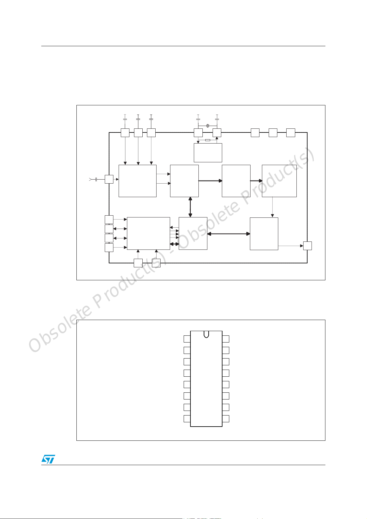
TDA7333 Block diagram and pin description
1 Block diagram and pin description
1.1 Block diagram
Figure 1. Block diagram
Cmpx
SCL_CLK
SDA_DATAIN
SA_DATAOUT
CSN
MPX
16
11
12
13
14
Cref Cref Cref
REF1
4 3 2
SIGMA DELTA
converter
REF3REF2
TEST LOGIC
&
PIN MUX's
resetn
tm
86
TM RESETN
16pF
10
Cxto
BANDPASS
filter
VDDA
Cxti
16pF
XTI XTO
9 1 5 7
OSCILLATOR
SINC4
filter
sinc4reg
sdaout
sdain
I2C/SPI
sck
interface
spi
testreg
VSS
INTERPOLATOR
RDS
demodulator &
synchronisation
VDDD
MPX
MPX
INTN
15
INTN
1.2 Pin description
Figure 2. Pin connection (top view)
VDDA
1
REF3
2
REF2
3
Obsolete Product(s) - Obsolete Product(s)
REF1
4
TDA7333
VSS
5
TM
6
7
RESETN
8
5/26
MPX
16
INTN
15
CSN
14
SA_DATAOUT
13
SDA_DATAIN
12
SCL_CLK
11
XTOVDDD
10
XTI
9
Obsolete Product(s) - Obsolete Product(s)
Block diagram and pin description TDA7333
Table 2. Pin description
Pin # Pin name Function
1 VDDA Analog supply voltage
2 REF3 Reference voltage 3 of A/D converter (2.65 V)
3 REF2 Reference voltage 2 of A/D converter (1.65 V)
4 REF1 Reference voltage 1 of A/D converter (0.65 V)
5 VSS Common ground
6TM
7 VDDD Digital supply voltage
8 RESETN External reset input (active low)
9 XTI Oscillator input
10 XTO Oscillator output
11 SCL_CLK Clock signal for I
12 SDA_DATAIN Data line in I
13 SA_DATAOUT Slave address in I
14 CSN Chip select (1 = I
15 INTN
Testmode selection (scan test).
Normal mode must be connected to gnd.
2
C and SPI modes
2
C mode, data input in SPI mode
2
C mode, data output in SPI mode
2
C mode, 0=SPI mode)
Interrupt output (active low), prog. at buff.not empty, buff. full, block A,B,D
,TA, TA EON
16 MPX Multiplex input signal
Obsolete Product(s) - Obsolete Product(s)
6/26
Obsolete Product(s) - Obsolete Product(s)
TDA7333 Electrical specifications
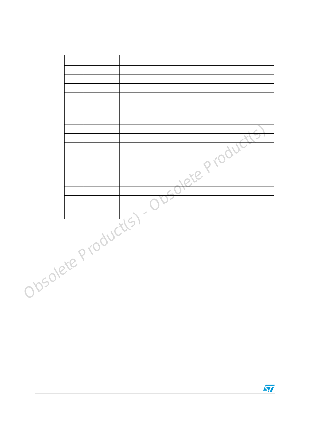
2 Electrical specifications
2.1 Quick reference
Table 3. Quick Reference
Symbol Parameter Min. Typ. Max. Unit
V
DDA/VDDD
T
S
V
(T
= 25 °C, VDDA/VDDD = 3.3 V, f
amb
Analog/digital power supply 3.0 3.3 3.6 V
amb
f
osc
I
dd
P
d
RDS
MPX
i Maximum speed in SPI mode 1 MHz
f
SP
f
i2c
Operating temperature -40 +85 °C
Quartz frequency
Total supply current 10 mA
Power dissipation 33 mW
RDS input sensitivity 1 mVrms
Input range of MPX signal 750 mVrms
Maximum speed in I2C mode 400 kHz
= 8.55 MHz)
osc
8.55 or
8.664
MHz
2.2 Absolute maximum ratings
Table 4. Absolute maximum ratings
Symbol Parameter Test conditions Min. Typ. Max. Unit
V
V
V
V
peak
3.3 V power supply voltages -0.5 4 V
DD
Input voltage 5 V tolerant inputs -0.5 5.5 V
in
Output voltage 5 V tolerant output buffers in tri-state -0.5 5.5 V
out
Maximum peak voltage 6 V
2.3 General interface electrical characteristics
Table 5. General interface electrical characteristics
Obsolete Product(s) - Obsolete Product(s)
Symbol Parameter Test conditions Min. Typ. Max. Unit
I
il
I
ih
I
oz
Low level input current Vi = 0 V 1 µA
High level input current Vi = V
V
= 0 V or V
Tri-state output leakage
o
= 5.5 V 1 3 µA
V
o
DD
DD
1µA
1µA
7/26
Obsolete Product(s) - Obsolete Product(s)
Electrical specifications TDA7333
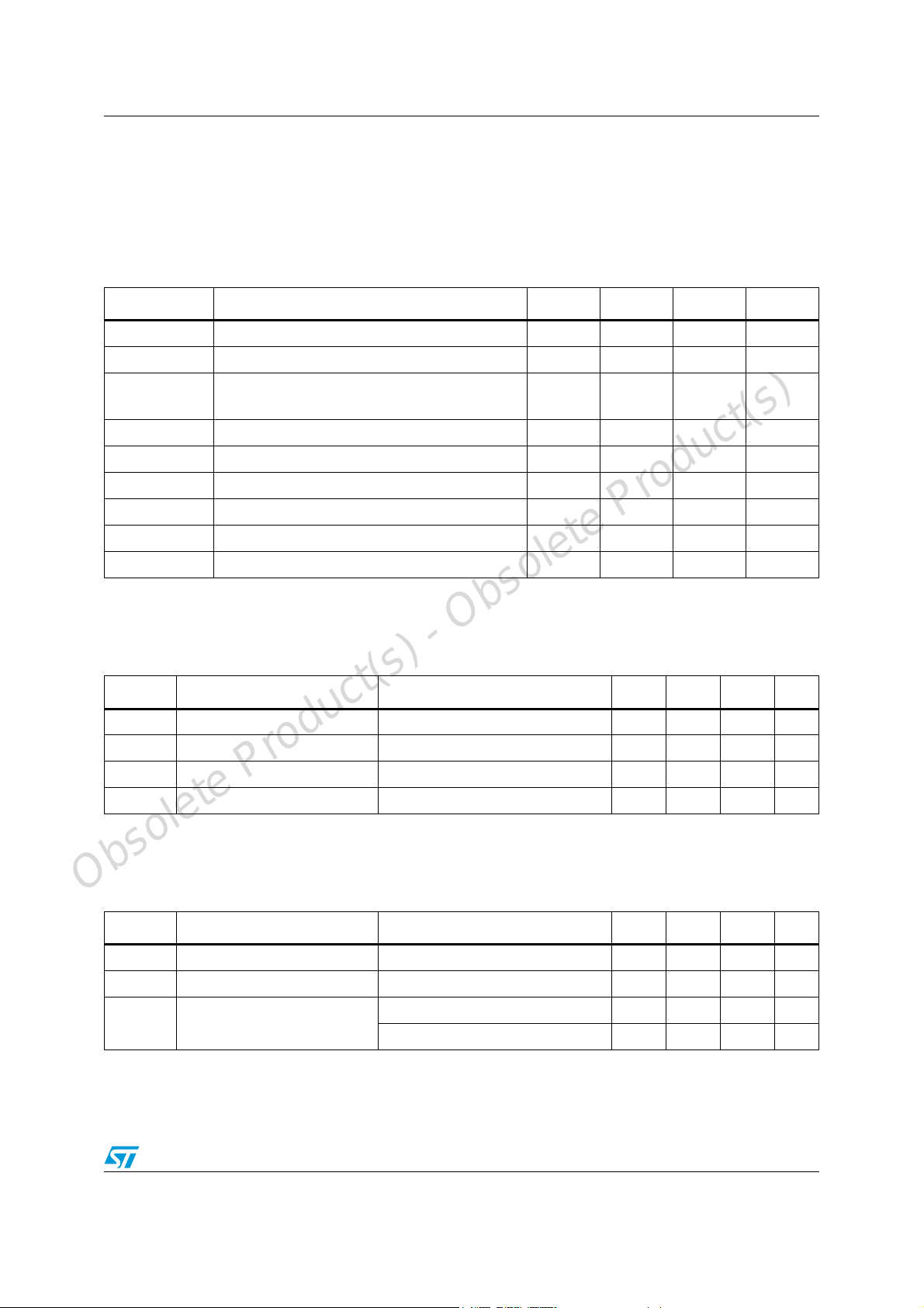
2.4 Electrical characteristics
Table 6. Electrical characteristics
Symbol Parameter Test conditions Min. Typ. Max. Unit
Supply (pin 1,5,7)
V
DDD
V
DDA
I
DDD
I
DDA
P
d
Digital inputs (pin 6,8,11,12,13,14)
V
il
V
ih
V
ilhyst
V
ihhyst
V
hst
Digital outputs (pin 12,13,15) are open drains
T
= -40 to +85 °C, V
amb
V
and V
DDD
Digital supply voltage 3.0 3.3 3.6 V
Analog supply voltage 3.0 3.3 3.6 V
Digital supply current 2 mA
Analog supply current 8 mA
Total power dissipation 33 mW
Low level input voltage 0.8 V
High level input voltage 2.0 V
Low level threshold input
falling
High level threshold input
rising
Schmitt trigger hysteresis 0.4 0.7 V
must not differ more than 0.15 V
DDA
DDA/VDDD
= 3.0 to 3.6 V, f
= 8.55 MHz, unless otherwise specified
osc
1.0 1.15 V
1.5 1.7 V
V
V
Analog inputs (pin 16)
V
MPX
S
R
Crystal parameters
Obsolete Product(s) - Obsolete Product(s)
f
g
C
xti,Cxto
t
High level output voltage
oh
Low level output voltage
ol
Input range of MPX signal 0.75 Vrms
RDS detection sensitivity 1 mVrms
RDS
Input Impedance of MPX pin 55k Ohm
MPX
Quartz frequency
osc
Start up time 10 ms
su
Transconductance 0.0006 A/V
m
Load capacitance 16 pF
Open drain, depends on external
circuitry
= 4 mA, takes into account
I
ol
200 mV drop in the supply voltage
8.55 or
8.664
V
DDD
0.4 V
V
MHz
8/26
Obsolete Product(s) - Obsolete Product(s)
TDA7333 Electrical specifications
Table 6. Electrical characteristics (continued)
T
= -40 to +85 °C, V
amb
V
and V
DDD
Symbol Parameter Test conditions Min. Typ. Max. Unit
Sigma delta modulator
must not differ more than 0.15 V
DDA
DDA/VDDD
= 3.0 to 3.6 V, f
= 8.55 MHz, unless otherwise specified
osc
F
OVR Oversampling ratio f = 57 kHz 38
THD+N
Sinc4/16 decimation filter
A57 Attenuation at 57 kHz -2.6 dB
Bandpass filter
R
f
stop
R
M
2
I
C
f
SPI
Sample rate f
s
Relative total harmonic dist.
plus noise
f
Decimated sample rate f
s
Attenuation difference BW = 54.5 to 59.5 kHz 0.4 dB
f
Sample rate f
s
f
Pass-band frequencies 55.6 58.4 kHz
p
Pass-band ripple -0.5 +0.5 dB
p
Stop-band corner frequencies 53.0 61 kHz
Stop-band attenuation -43 dB
s
Interpolation factor 32
i
Clock frequency in I2C mode 400 kHz
I2C
= 8.55 MHz 4.275 MHz
osc
BW = 54.5 to 59.5 kHz,
unweigted, V
= 8.55 MHz 267.2 kHz
osc
= 8.55 MHz 267.2 kHz
osc
= 3 mVrms
rds
27 dB
f
SPI
t
t
t
t
odv
Obsolete Product(s) - Obsolete Product(s)
t
t
Clock frequency in SPI mode 1 MHz
Clock high time 450 ns
ch
Clock low time 450 ns
t
cl
Chip select setup time 500 ns
csu
Chip select hold 500 ns
csh
Output data valid 250 ns
Output hold 0 ns
oh
Deselect time 1000 ns
t
d
Data setup time 200 ns
su
t
Data hold time 200 ns
h
9/26

Obsolete Product(s) - Obsolete Product(s)
Functional description TDA7333
3 Functional description
3.1 Overview
The new RDS/RBDS processor contains all RDS/RBDS relevant functions on a single chip.
It recovers the inaudible RDS/RBDS information which are transmitted on most FM radio
broadcasting stations.
Due to an integrated 3
further processing is done in the digital domain and therefore very economical. After filtering
the highly oversampled output of the A/D converter, the RDS/RBDS demodulator extracts
the RDS DataClock, RDS Data Signal and the Quality information. A next RDS/RBDS
decoder will synchronize the bitwise RDS stream to a group and block wise information.
This processing includes an error detection and error correction algorithm. In addition, an
automatic flywheel control avoids exhaustive data exchange between the RDS/RBDS
processor and the host.
The device operates in accordance with the EBU (European Broadcasting Union)
specifications.
3.2 Sigma delta converter
rd
order sigma delta converter, which samples the MPX signal, all
The sigma delta modulator is a 3rd order (second order-first order cascade) structure.
Therefore a multibit output (2 bit streams) represents the analog input signal. A next digital
noise canceller will take the 2 bit streams and calculates a combined stream which is then
fed to the decimation filter. The modulator works at a sampling frequency of XTI/2. The
oversampling factor in relation to the band of interest (57 kHz ±2.4 kHz) is 38.
3.3 Sinc4/16 decimation filter
The oversampled data delivered from the modulator are decimated by a value of 16 with a
th
4
order Sinc Filter.
This is considered to be the optimum solution for high decimation factors and for a 3
sigma delta modulator.
The architecture is a very economical implementation because digital multipliers are not
required. It is implemented by cascading 4 integrators operating at full sampling rate (XTI/2)
followed by 4 differentiates operating at the reduced sampling rate (XTI/2/16). Also wrap
around logic is allowed and the internal overflow will not affect the output signal as long as a
minimum required bit width is maintained.
Obsolete Product(s) - Obsolete Product(s)
The transfer function of this Sinc4/16 filter is:
Hz()
=
1z
–
--------------------
1z
–
M–
1–
⎛⎞
1
---- -
⎜⎟
M
⎝⎠
K
rd
order
with K = 4, M = 16
10/26

Obsolete Product(s) - Obsolete Product(s)
TDA7333 Functional description
and its frequency response is:
K
Mω
⎛⎞
Hejω()
=
⎛⎞
⎜⎟
⎜⎟
⎜⎟
⎝⎠
sin
1
-----------------------
---- -
M
sin
-------- -
⎝⎠
2
ω
⎛⎞
--- -
⎝⎠
2
with
f
ω 2π
---- -
=
fs
Figure 3. Transfer function of a 4
0
10
20
30
40
50
Magnitude [dB]
60
70
80
90
100
0 0.2 0.4 0.6 0.8 1 1.2 1.4 1.6 1.8 2
th
order sinc. filter, decimation factor is 16.
Sinc4/16 Transfer Function
Frequency [Hz]
x 10
6
Figure 4. Magnitude response of sinc. 4/16 filter in RDS band
0
0.5
1
1.5
2
2.5
Magnitude [dB]
3
Obsolete Product(s) - Obsolete Product(s)
3.5
4
4.5
5
5.4 5.5 5.6 5.7 5.8 5.9 6
Sinc4/16 Transfer Function (RDS Band)
Frequency [Hz]
x 10
4
11/26

Obsolete Product(s) - Obsolete Product(s)
Functional description TDA7333
3.4 RDS bandpass filter and interpolator
The 8th order digital RDS bandpass filter is of type Tschebyscheff and centered at 57 kHz.
With linear phase characteristics in the passband and approximately flat group delay it
guarantees best filter function of the RDS and ARI signal. Four biquads are cascaded
working at a common sampling frequency of XTI/2/16.
Figure 5. Transfer function of RDS bandpass filter
10
0
10
20
30
40
50
Magnitude [dB]
60
70
80
90
100
4 4.5 5 5.5 6 6.5 7
Transfer Function of RDS Filter
Frequency [Hz]
x 10
4
Figure 6. Phase response of the RDS bandpass filter
3
2
1
0
Phase [Radians]
1
2
3
5.6 5.65 5.7 5.75 5.8
Obsolete Product(s) - Obsolete Product(s)
Phase of RDS Filter
Frequency [Hz]
x 10
4
The output sample of the bandpass filter is picked up from a linear interpolator with sinc2
characteristics. The interpolation factor is 32. A zero cross detection is simply formed by
taking the sign bit of the interpolated signal. This signal which contains only phase
informations is processed by the RDS Demodulator.
12/26

Obsolete Product(s) - Obsolete Product(s)
TDA7333 Functional description
3.5 Demodulator
The demodulator includes:
● RDS quality indicator with selectable sensitivity
● Selectable time constant of 57 kHz PLL
● Selectable time constant of bit PLL
● time constant selection done automatically or by software
Figure 7. Demodulator block diagram
MPX
mclk
(8,550 or 8,664 MHz)
to RDS group and block synchronisation
from RDS group and block synchronisation
module:
RD
RDSDAT
RDSQUAL
module:
AR_RES
Input-stage
(digital Filter)
Sine comp.
Cosine comp.
Half Wave
Integrator
ARI-indicator
mclk
57 kHz PLL
Clock Generator
1187.5Hz
PLL
Half Wave
Extractor
frequency
offset comp.
RDS Data
Extractor
RDS Quality
Extractor
The demodulator is fed by the 57 kHz bandpass filter and interpolated multiplex signal. The
input signal passes a digital filter extracting the sinus and cosinus components, to be used
for further processing.
The sign of both channels are used as input for the ARI indicator and for the 57 kHz PLL.
A fast ARI indicator determines the presence of an ARI carrier. If an ARI carrier is present,
the 57 kHz PLL is operating as a normal PLL, else it is operating as a Costas loop.
One part of the PLL is compensating the integral offset (frequency deviation between
oscillator and input signal).
One channel of the filter is fed into the half wave integrator. Two half waves are created, with
a phase deviation of 90 degrees. One wave represents the RDS component, whereas the
other wave represents the ARI component. The sign of both waves are used as reference
for the bit PLL (1187.5 Hz).
Obsolete Product(s) - Obsolete Product(s)
The RDS wave is then fed into the half wave extractor. This leads into an RDS signal, which
after integration and differential decoding represents the RDS data.
In a similar way a quality bit can be calculated. This is useful to optimize error correction.
The module needs a fixed clock of 8.55 MHz. Optionally an 8.664 MHz clock may be used
by setting the corresponding bit in rds_bd_ctrl register (see Chapter 3.7.6).
In order to optimize the error correction in the group and block synchronization module, the
sensitivity level of the quality bit can be adjusted in three steps (see Chapter 3.7.6). Only
13/26

Obsolete Product(s) - Obsolete Product(s)
Functional description TDA7333
bits marked as bad by the quality bit are allowed to be corrected in the group and block
synchronization module. Thus the error correction is directly influenced by this setup.
The time constant of the 57 kHz PLL and the 1187.5 Hz PLL may be influenced by software
(see Chapter 3.7.6).
This is useful in order to achieve a fast synchronization after a program resp. frequency
change (fast time constant) and to get a maximum of noise immunity after synchronization
(slow time constant).
The user may choose between 2 possibilities via bit rds_bd_ctrl[1] (see Chapter 3.7.6):
1. Hardware selected time constant - In this case both pll time constants are reset to the
fastest one with a reset from the group and block synchronization module. If the
software decides to re synchronize, it generates a reset. Both PLL are set to the fastest
time constant, which is automatically increased to the slowest one. This is done in four
steps within a total time of 215.6 ms (256 RDS clocks).
2. Software selected time constant - In this case the time constant of both PLL can be
selected individually by software.PLL time constants can be set independently.
3.6 Group and block synchronization module
The group and block synchronization module has the following features:
● Hardware group and block synchronization
● Hardware error detection
● Hardware error correction using the quality bit information of the demodulator
● Hardware synchronization flywheel
● TA information extraction
● reset by software (ar_res)
Figure 8. Group and block synchronization block diagram
RDSCLK
RDSDAT
RDSQAL
from RDS
Demodulator
Obsolete Product(s) - Obsolete Product(s)
BLOCK A
BLOCK B
BLOCK D
AR_RES
TAEON
TA
rds_bd_h,rds_bd_l
read only read only read only
RDSDAT(15:0)
Syndrome register
Correction
logic
Quality bit counter
RDS block counter
14/26
Group & Block Synchr oniza tion Co ntro l Bloc k
rds_corrp rds_qu rds_int
S(4:0)
CP(9:5)
Corrected
Data_OK
Syndrom zero
ABH
DBH
BLOCKE detected
S(9:0)
Correct. pat.
Block
misse d
Q(3:0)
QU(0:3)
next
RDS
bit
bit_int
set set
read/write
BLOCK D
BLOCK B
BLOCK A
new
Block
availabl e
res
int
synch. AR_RES
TAEON
TA

Obsolete Product(s) - Obsolete Product(s)
TDA7333 Functional description
This module is used to acquire group and block synchronization of the received RDS data
stream, which is provided in a modified shortened cyclic code. For the theory and
implementation of the modified shortened cyclic code, please refer to the specification of the
radio data system (RDS) EN50067.
It further detects errors in the data stream. Depending on the quality bit information of the
demodulator an error correction is made.
The RDS data bytes are available to the software together with status bits giving an
indication on the reliability of the data.
It also extracts TA information which can be used as interrupt source (see Chapter 3.7.1).
3.7 Programming through serial bus interface
The serial bus interface is used to access the different registers of the chip. It is able to
handle both I
thanks to the pin CSN:
● if the pin CSN is high, the interface operates as an I
● if the pin CSN is asserted low, the interface operates as a SPI bus.
In both modes, the device is a slave, i.e the clock pin SCL_CLK is only an input for the chip.
Depending on the transfer mode, external pins have alternate functions as following:
Table 7. External pins alternate functions
SCL_CLK CLK (serial clock) SCL (serial clock)
SDA_DATAIN DATAIN (data input) SDA (data line)
SA_DATAOUT DATAOUT (data output) SA (slave address)
Eight registers are available with read or read/write access rights as the following:
Table 8. Registers description
rds_int[7:0] (see 3.7.1) read/write Interrupt source setting, sync., bne information
rds_qu[7:0] (see 3.7.2) read Quality counter, actual block name
2
C and SPI transfer protocols, the selection between the two modes is done
2
C bus.
Pin Function in SPI mode (CSN =0) Function in I2C mode (CSN=1)
Register
Access
rights
Function
rds_corrp[7:0] (see 3.7.3) read Error correction status, buffer ovf information
Obsolete Product(s) - Obsolete Product(s)
rds_bd_h[7:0] (see 3.7.4) read High byte of current RDS block
rds_bd_l[7:0] (see 3.7.5) read Low byte of current RDS block
rds_bd_ctrl[7:0] (see 3.7.6) read/write Frequency, quality sensitivity, demodulator pll settings
sinc4reg[7:0] read/write Sinc4 filter settings (for internal use only)
testreg[7:0] read/write Test modes (for internal use only)
The meaning of each bit is described below:
15/26

Obsolete Product(s) - Obsolete Product(s)
Functional description TDA7333
3.7.1 rds_int register
Figure 9. rds_int register
rds_int
bit 7 bit 6 bit 5 bit 4 bit 3 bit 2 bit 1 bit 0
reset value
bit name
access
(1)
write bne ar_res synch itsrc2 itsrc1 itsrc0 int
r/w r r/w r r/w r/w r/w r
interrupt source i tsrc2 itsrc1 itsrc0
no interrupt
RDS Block
block A
block B
block D
TA
TAEON
3.7.2 rds_qu register
00
00
001
101
010
011
110
111
00000
0
0
interrupt bit. It is set to one on every programmed interrupt. It
is reset by reading rds_int register.
interrupt source
itsrc[2:0] select the interrupt source
synchronization information.
1: the module is already synchronized.
0: the module is synchronizing
It is used to force a resynchronization. If it is set to one, the
RDS modules are forced to resynchronization state.
The bit is automatically reset. So it is always read as zero.
RDS block.
if 1, one block has been detected
rds_int and rds_bd_ctrl write order (
1: rds_int and rds_bd_ctrl are updated with data shifted in.
0: rds_int and rds_bd_ctrl are not updated.
Note : when changing the interrupt mode, one has to
perform a reset of the module (i.e set the bit “ar_res” at
one)
(1)
when in SPI mode
)
Figure 10. rds_qu register
rds_qu
reset value
bit name
acc ess
Obsolete Product(s) - Obsolete Product(s)
bit 7 bit 0bit 1bit 2bit 3bit 4bit 5bit 6
0
00
r
rr
(2)
block name
block A
block B
block D
000
rrr
blk1
blk0
00
10
1block C,C’ 0
11
0
0
synzequ0qu3 qu1qu2 blk1 blk0
r
r
It indicates if the error correction was successfull.
1: the syndrome was zero after the error correction.
0: the syndrome did not become zero and therefore the
correction was not successfull.
1: a block E is detected.This indicates a paging block
which is defined in the RBDS specification used in the
united states of America.
0: an ordinary RDS block A, B, C, c·or D is detected, or no
valid syndrome was found.
bit 0 of block counter (2)
bit 1 of block counter (2)
bit 0 of quality counter
bit 1 of quality counter
bit 2 of quality counter
bit 3 of quality counter
(3) qu[3..0] is a counter of the quality bit information coming
from the RDS demodulator. It is counting the number of bits
which are marked as bad by the demodulator. Only those bits
are allowed to be corrected. Thus the quality bit counter indicates the maximum possible number of bits being corrected.
(3)
(3)
(3)
(3)
16/26

Obsolete Product(s) - Obsolete Product(s)
TDA7333 Functional description
3.7.3 rds_corrp register
Figure 11. rds_corrp register
rds_comp bit 7 bit 6 bit 5 bit 4 bit 3 bit 2 bit 1 bit 0
reset value 0 0 0 0 0 0 0 0
bit name cp9 cp8 cp7 cp6 cp5
access r r r r r r r r
correct data_ok
-
It is an information about a correct syndrome after reception resp. after an error correction routine.
1: a correct syndrome was detected.
0: the syndrome was wrong. The current RDS data cannot
be used.
It is an information about error correction.
1: an error correction was made.
0: the actual RDS block is detected as error free.
bit 5 of the syndrome register(*)
bit 6 of the syndrome register(*)
bit 7 of the syndrome register(*)
bit 8 of the syndrome register(*)
bit 9 of the syndrome register(*)
(*) (refer to: Specification of the radio data system EN50067
of CENELEC, ANNEX B). When bits 4...0 of the syndrome
register are all zero a possible error burst is stored in this
bits. With the help of the correction pattern(bits 9..5 of the
syndrome register), the type of error can be measured in order to classify the reliability of the correction.
3.7.4 rds_bd_h register
Figure 12. rds_bd_h register
rd s_ b d _h
reset value
bit name
access
Obsolete Product(s) - Obsolete Product(s)
bit 7 bit 0bit 1bit 2bit 3bit 4bit 5bit 6
0
00
r
rr
000
rrr
0
r
0
m8m9m12m15 m13m14 m11 m10
r
bit 15 of the actual RDS 16bits information
bit 14 of the actual RDS 16bits information
bit 13 of the actual RDS 16bits information
bit 12 of the actual RDS 16bits information
bit 11 of the actual RDS 16bits information
bit 10 of the actual RDS 16bits information
bit 9 of the actual RDS 16bits information
bit 8 of the actual RDS 16bits information
17/26

Obsolete Product(s) - Obsolete Product(s)
Functional description TDA7333
3.7.5 rds_bd_l register
Figure 13. rds_bd_l register
rds_bd_I
reset value
bit name
access
bit 7 bit 0bit 1bit 2bit 3bit 4bit 5bit 6
0
00
r
rr
000
rrr
0
r
0
m0m1m4m7 m5m6 m3 m2
r
bit 7 of the actual RDS 16bits information
bit 6 of the actual RDS 16bits information
bit 5 of the actual RDS 16bits information
bit 4 of the actual RDS 16bits information
bit 3 of the actual RDS 16bits information
bit 2 of the actual RDS 16bits information
bit 1of the actual RDS 16bits information
bit 0 of the actual RDS 16bits information
3.7.6 rds_bd_ctrl register
Figure 14. rds_bd_ctrl register
rds_bd_ctrl bit 7 bit 6 bit 5 bit 4 bit 3 bit 2 bit 1 bit 0
reset value
bit name
access
(1)
Obsolete Product(s) - Obsolete Product(s)
(2)
pllb1 pllb0
0
00
r/w r/w r/w r/w r/w r/w r/w
pllf
lock time needed for 90 deg deviation
0
1
lock time needed for 90 deg deviation
00
10
10
11
10 ms
5 ms (reset status)
15 ms
35 ms
76 ms
00 0
pllb0freq qsens1qsens0 pllf
2 ms
1
0
shw -pllb1
r
select PLL’s time constants by software or hardware:
1: software. Time constants are selected by pllb[1:0] resp.
pllf
0: hardware. (reset value) Time constants automatically
increase after a reset.
set the 57kHz pll time constant
bit 0 of 1187.5Hz pll time constant
bit 1 of 1187.5Hz pll time constant
bit 0 of quality sensitivity
bit 1 of quality sensitivity
select oscillator frequency:
1: 8.664MHz
0: 8.55MHz (reset value)
(3)
select sensitivity of quality bit.
00: minimum (reset value)
11: m a xim u m
(1)
(2)
(2)
(3)
(3)
Note: Sinc4reg and testreg are reserved registers dedicated to testing and evaluation.
18/26

Obsolete Product(s) - Obsolete Product(s)
TDA7333 Functional description
3.8 I2C transfer mode
This interface consists of three lines: a serial data line (SDA), a bit clock (SCL), and a slave
address select (SA).
The interface is capable of operating in fast mode (up to 400kbits/s) but also at lower rates
(<100kbits/s).
Data transfers follow the format shown in Figure 15. After the START condition (S), a slave
address is sent. The address is 7 bits long followed by an eighth bit which is a data direction
bit (R/_W).
A ’zero’ indicates a transmission (WRITE), a ’one’ indicates a request for data (READ).
The slave address of the chip is set to 001000S, where S is the least significant bit of the
slave address set externally via the pin SA_DATAOUT. This allows to choose between two
addresses in case of conflict with another device of the radio set.
Each byte has to be followed by an acknowledge bit (SDA low).
Data is transferred with the most significant (MSB) bit first.
A data transfer is always terminated by a stop condition (P) generated by the master.
Figure 15. I
2
C data transfer
SDA
SCL
S P
START
CONDITION
1-7 8
ADDRESS R/W ACK DAT A ACK DATA
91-7891-7 8
9
ACK/ACK
STOP
CONDITION
3.8.1 Write transfer
Figure 16. I2C write transfer
S Slave address rds_int AA A sinc4reg A PW testreg
from master to slave
from slave to master
Obsolete Product(s) - Obsolete Product(s)
Figure 17. I
SA
0
1
CSN
SDA
2
C write operation example: write of rds_int and rds_bd_ctrl registers
rds_b d_ctrl
S = start condition
W = write mode
Slave address = 001000S ( where S is the level of the pin
A = acknowledge bit
P = stop condition
rds_int[7:0]
SA_DATAOUT)
rds_bd_ctrl[7:0]
A
SCL
START
CONDITION
S
SLAVE ADDRESS
WACK
ACK ACK
P
STOP
CONDITION
19/26

Obsolete Product(s) - Obsolete Product(s)
Functional description TDA7333
3.8.2 Read transfer
Figure 18. I2C read transfer
S Slave address rds_int A rds_quA A testreg A P
R
S = start condition
R = read mode
from master to slave
from slave to master
Slave address = 001000S ( where S is the level of the pin
SA_DATAOUT)
A = acknowledge bit
P = stop condition
Eight bytes can be read at a time (please refer to Section 3.7 for the meaning of each bit).
The master has always the possibility to read less than eight registers by not sending the
acknowledge bit and then generating a stop condition after having read the needed amount
of registers.
There are two typical read access:
● read only the first register rds_int to check the interrupt bit.
● read the first five registers rds_int, rds_qu, rds_corrp, rds_bd_h, rds_bd_l to get the
RDS data
The registers are read in the following order: rds_int, rds_qu, rds_corrp, rds_bd_h,rds_bd_l,
rds_bd_ctrl, sinc4reg, testreg.
Figure 19. I
SA
0
1
CSN
2
C read access example 1: read of 5 bytes
SDA
SCL
S
SLAVE ADDRESS
START
CONDITION
Figure 20. I
2
C read access example 2: read of 1 byte
Obsolete Product(s) - Obsolete Product(s)
RACK
SA
CSN
SDA
SCL
0
1
S
START
CONDITION
rds_int[7:0]
SLAVE ADDRESS
rds_qu[7:0]
ACK ACK
RACK
rds_corrp[7:0]
rds_int[7:0]
rds_bd_h[7:0]
ACK ACK ACK
ACK
STOP
CONDITION
rds_bd_l[7:0]
P
P
STOP
CONDITION
20/26

Obsolete Product(s) - Obsolete Product(s)
TDA7333 Functional description
3.9 SPI mode
Figure 21. SPI data transfer
CSN
CLK
DATAIN
DATAOUT
update of
shiftregister with
registers content
t
csu
t
su
rds_int[7] testreg[0]rds_int[6] rds_int[0]rds_int[1]rds_int[2]rds_int[3]rds_int[4]rds_i nt[5] testreg[1]
shift of DATAIN
in shiftregister
t
h
t
odvtoh
2
tclt
ch
64638765431
rds_int[0]rds_int[1]
content if reque sted
t
d
t
csh
update of regi sters
with shiftregister
This interface consists of four lines. A serial data input (DATAIN), a serial data output
(DATAOUT), a chip select input (CSN) and a bit clock input (CLK).
The chip select input signals the begin and end of the data transfer. If the data transfer
starts, at each
bit clock one bit is clocked out via the serial data output and one bit is clocked in via the
serial data input.
When chip enable signals the begin of the data transfer the internal 64 bits shift register is
updated with the current registers content of the V324.
When chip enable signals the end of the data transfer the registers with write access can be
updated with the bits which have been last shifted in.
The last byte on DATAIN input is always rds_int[7:0] and the former last one is
rds_bd_ctrl[7:0]. In other words, the master has to take in account the amount of bytes
transmitted when intending to perform a write operation so that the last two bytes sent on
DATAIN are rds_bd_ctrl[7:0] and rds_int[7:0].
If the update of both rds_int and rds_bd_ctrl registers is actually taking place depends on
the MSB of rds_int, i.e. rds_int[7] = 0 - no update, rds_int[7] = 1 update of both registers.
Hereafter you can find typical read/write access in SPI mode:
Figure 22. Write rds_int and rds_bd_ctrl registers in SPI mode, reading RDS data
and related flags
CSN
Obsolete Product(s) - Obsolete Product(s)
CLK
DATAIN
DATAOUT
{1,rds_int[6:0]}rds_bd_c trl[7:0]
rds_int[7:0] rds_qu[7:0] rds_corrp[7:0] rds_bd_h[7:0] rds_bd_l[7:0]
21/26

Obsolete Product(s) - Obsolete Product(s)
Functional description TDA7333
Figure 23. Read out RDS data and related flags, no update of rds_int and
rds_bd_ctrl registers
CSN
CLK
DATAIN
DATAOUT
rds_int[7:0] rds_qu[7:0] rds_corrp[7:0] rds_bd_h[7:0] rds_bd_l[7:0]
{0,x,x,x,x,x,x,x}
Figure 24. Write rds_int registers in SPI mode, reading 1 register
CSN
CLK
DATAIN
DATAOUT
{1,rds_int[6 :0]}
rds_int[7:0]
The content of the rds registers is clocked out on DATAOUT pin in the following order:
rds_int[7:0], rds_qu[7:0], rds_corrp[7:0], rds_bd_l[7:0], rds_bd_h[7:0], rds_ctrl[7:0],
sinc4reg[7:0], testreg[7:0]
For the meaning of the single bits please refer to the Section 3.7.
Note: After 40 bit clocks the whole RDS data and flags are clocked out.
Obsolete Product(s) - Obsolete Product(s)
22/26

Obsolete Product(s) - Obsolete Product(s)
TDA7333 Application notes
4 Application notes
A typical rds data transfer could work like this:
1. The micro sets the interrupt source to “RDS block” interrupt by setting itsrc[2:0] to 001.
2. The micro continuously checks the rds_int[7:0] bits for the first interrupt (rds_int[0] goes
high). If there is no interrupt it stops the transfer after these 8 bits. No update of the
rds_int[7:0] is performed.
3. Once there is an interrupt detected the micro will also clock out all the other RDS bits
(rds_qu[7:0], rds_corrp[7:0], rds_bd_h[7:0], rds_bd_l[7:0]).
4. The next interrupt can not be expected before 22ms.
The above example is working by polling the rds_int[0] bit. An easier and better application
is possible by checking the RDS interrupt pin INTN (see below) and starting the transfer only
when this interrupt is present.
The output pin INTN acts as an interrupt pin. The source of interrupt is programmable
through the register rds_int (see Section 3.7.1), the value on the pin is the inverted value of
the bit rds_int[0] (i.e this interrupt pin is active low). With the help of this pin an interrupt
driven request of the rds data is possible (the external processor only starts the transfer if an
interrupt is active).
Obsolete Product(s) - Obsolete Product(s)
23/26

Obsolete Product(s) - Obsolete Product(s)
Package information TDA7333
5 Package information
In order to meet environmental requirements, ST (also) offers these devices in ECOPACK®
packages. ECOPACK® packages are lead-free. The category of second Level Interconnect
is marked on the package and on the inner box label, in compliance with JEDEC Standard
JESD97. The maximum ratings related to soldering conditions are also marked on the inner
box label.
ECOPACK is an ST trademark. ECOPACK specifications are available at: www.st.com.
Figure 25. TSSOP16 mechanical data and package dimensions
DIM.
A 1.200 0.047
A1 0.050 0.150 0.002 0.006
A2 0.800 1.000 1.050 0.031 0.039 0.041
b 0.190 0.30 0 0.007 0.012
c 0.090 0.200 0.005 0.009
D (1) 4.900 5.000 5.100 0.114 0.118 0.122
E 6.200 6.400 6.600 0.244 0.252 0.260
E1 (1) 4.300 4.400 4.500 0.170 0 .173 0.177
e 0.6 50 0 .026
L 0.450 0.600 0.75 0 0.018 0 .024 0.030
L1 1.000 0.039
k 0˚ (min.) 8˚ (max.)
aaa 0.100 0.004
Note: 1. D and E1 does not include mold flash or protrusions.
mm inch
MIN. TYP. MAX. MIN. TYP. MAX.
Mold flash or potrusions shall not exceed 0.15mm
(.006inch) p er side.
OUTLINE AND
MECHANICAL DATA
TSSOP16
(Body 4.4mm)
Obsolete Product(s) - Obsolete Product(s)
0080338 (Jedec MO-153-AB)
24/26

Obsolete Product(s) - Obsolete Product(s)
TDA7333 Revision history
6 Revision history
Table 9. Document revision history
Date Revision Changes
25-Jun-2008 1 Initial release.
Obsolete Product(s) - Obsolete Product(s)
25/26

Obsolete Product(s) - Obsolete Product(s)
TDA7333
Please Read Carefully:
Information in this document is provided solely in connection with ST products. STMicroelectronics NV and its subsidiaries (“ST”) reserve the
right to make changes, corrections, modifications or improvements, to this document, and the products and services described herein at any
time, without notice.
All ST products are sold pursuant to ST’s terms and conditions of sale.
Purchasers are solely responsible for the choice, selection and use of the ST products and services described herein, and ST assumes no
liability whatsoever relating to the choice, selection or use of the ST products and services described herein.
No license, express or implied, by estoppel or otherwise, to any intellectual property rights is granted under this document. If any part of this
document refers to any third party products or services it shall not be deemed a license grant by ST for the use of such third party products
or services, or any intellectual property contained therein or considered as a warranty covering the use in any manner whatsoever of such
third party products or services or any intellectual property contained therein.
UNLESS OTHERWISE SET FORTH IN ST’S TERMS AND CONDITIONS OF SALE ST DISCLAIMS ANY EXPRESS OR IMPLIED
WARRANTY WITH RESPECT TO THE USE AND/OR SALE OF ST PRODUCTS INCLUDING WITHOUT LIMITATION IMPLIED
WARRANTIES OF MERCHANTABILITY, FITNESS FOR A PARTICULAR PURPOSE (AND THEIR EQUIVALENTS UNDER THE LAWS
OF ANY JURISDICTION), OR INFRINGEMENT OF ANY PATENT, COPYRIGHT OR OTHER INTELLECTUAL PROPERTY RIGHT.
UNLESS EXPRESSLY APPROVED IN WRITING BY AN AUTHORIZED ST REPRESENTATIVE, ST PRODUCTS ARE NOT
RECOMMENDED, AUTHORIZED OR WARRANTED FOR USE IN MILITARY, AIR CRAFT, SPACE, LIFE SAVING, OR LIFE SUSTAINING
APPLICATIONS, NOR IN PRODUCTS OR SYSTEMS WHERE FAILURE OR MALFUNCTION MAY RESULT IN PERSONAL INJURY,
DEATH, OR SEVERE PROPERTY OR ENVIRONMENTAL DAMAGE. ST PRODUCTS WHICH ARE NOT SPECIFIED AS "AUTOMOTIVE
GRADE" MAY ONLY BE USED IN AUTOMOTIVE APPLICATIONS AT USER’S OWN RISK.
Resale of ST products with provisions different from the statements and/or technical features set forth in this document shall immediately void
any warranty granted by ST for the ST product or service described herein and shall not create or extend in any manner whatsoever, any
liability of ST.
ST and the ST logo are trademarks or registered trademarks of ST in various countries.
Information in this document supersedes and replaces all information previously supplied.
Obsolete Product(s) - Obsolete Product(s)
The ST logo is a registered trademark of STMicroelectronics. All other names are the property of their respective owners.
© 2008 STMicroelectronics - All rights reserved
STMicroelectronics group of companies
Australia - Belgium - Brazil - Canada - China - Czech Republic - Finland - France - Germany - Hong Kong - India - Israel - Italy - Japan -
Malaysia - Malta - Morocco - Singapore - Spain - Sweden - Switzerland - United Kingdom - United States of America
www.st.com
26/26

 Loading...