


STMicroelectronics ESDA14V2L, ESDA25L, ESDA5V3L, ESDA6V1L Schematic [ru]
®
ESDAxxL
Application Specific Discretes
A.S.D.
APPLICATIONS
Where transient overvoltage protection in ESD
sensitive equipment is required, such as :
- COMPUTERS
- PRINTERS
- COMMUNICATION SYSTEMS
It is particulary recommended for the RS232 I/O
port protection where the line interface withstands
only with 2kV ESD surges.
FEATURES
2 UNIDIRECTIONAL TRANSIL FUNCTIONS.
n
LOW LEAKAGE CURRENT : IRmax. < 20µAat
n
.
V
BR
300 W PEAK PULSE POWER (8/20µs)
n
DESCRIPTION
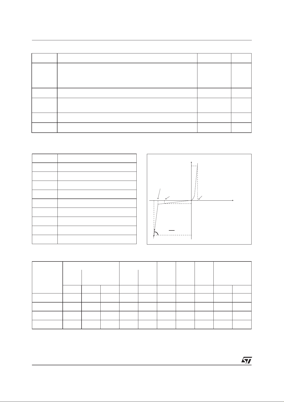
The ESDAxxL is a dual monolithic voltage
suppressordesignedtoprotectcomponentswhich
are connected to data and transmission lines
against ESD.
It clamps the voltage just above the logic level
supply for positive transients, and to a diode drop
below ground for negative transients.
It can also work as bidirectionnal suppressor by
connecting only pin1 and 2.
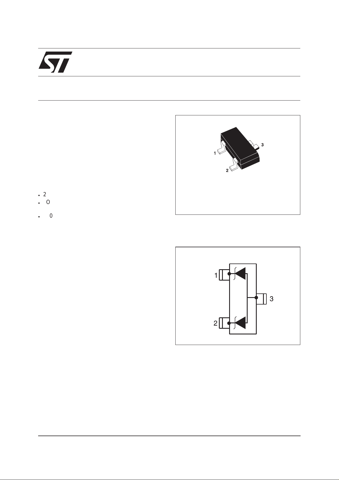
DUAL TRANSIL ARRAY
FOR ESD PROTECTION
SOT23
FUNCTIONAL DIAGRAM
BENEFITS
High ESD protection level : up to 25 kV.
High integration.
Suitable for high density boards.
COMPLIESWITHTHEFOLLOWINGSTANDARDS :
IEC61000-4-2 level 4
MIL STD 883C-Method 3015-6 : class 3.
(human body model)
Marchr 2000 - Ed: 4A
1/6
ESDAxxL
ABSOLUTE MAXIMUM RATINGS (T
amb
= 25°C)
Symbol Parameter Value Unit
V
PP
P
PP
T
stg
T
j
T
L
T
op
note 1: Evolution of functional parameters is given by curves.
ELECTRICAL CHARACTERISTICS (T
Symbol Parameter
V
RM
V
BR
V
CL
I
RM
I
PP
Electrostatic discharge
MIL STD 883C - Method 3015-6
IEC61000-4-2 air discharge
IEC61000-4-2 contact discharge
Peak pulse power (8/20 µs)
Storage temperature range
Maximum junction temperature
Maximum lead temperature for soldering during 10s
Operating temperature range
= 25°C)
amb
Stand-off voltage
Breakdown voltage
Clamping voltage
Leakage current
V
BR
V
Peak pulse current
RM
25
16
9
300 W
-55to+150
150
260 °C
-40to+125 °C
I
I
F
V
F
I
RM
kV
°C
°C
V
αT
C
Rd
V
F
Types VBR@
ESDA5V3L
ESDA6V1L
ESDA14V2L
ESDA25L
note 1 : Square pulse Ipp = 15A, tp=2.5µs.
note 2 : ∆ VBR= αT* (Tamb -25°C) * VBR(25°C)
Voltage temperature coefficient
Capacitance
Dynamic resistance
Forward voltage drop
min. max. max. typ. max. typ. max.
VVmAµAV
5.3 5.9 1 2 3 280 5 220 1.25 200
6.1 7.2 1 20 5.25 350 6 140 1.25 200
14.2 15.8 1 5 12 650 10 90 1.25 200
25 30 1 1 24 1000 10 50 1.2 10
1
Slope:
Rd
I
R
IRM@V
RM
Rd αTC V
note 1 note 2 0V bias
10-4/⊃CpF V mA
Ω
m
I
PP
@I
F
F
2/6
CALCULATION OF THE CLAMPING VOLTAGE
USE OF THE DYNAMIC RESISTANCE
The ESDA family has been designed to clamp fast
spikes like ESD. Generally the PCB designers
need to calculate easily the clamping voltage V
CL
This is why we give the dynamic resistance in
addition to the classical parameters. The voltage
across the protection cell can be calculated with
the following formula:
=VBR+RdI
V
CL
PP
WhereIpp is thepeak current throughthe ESDA cell.
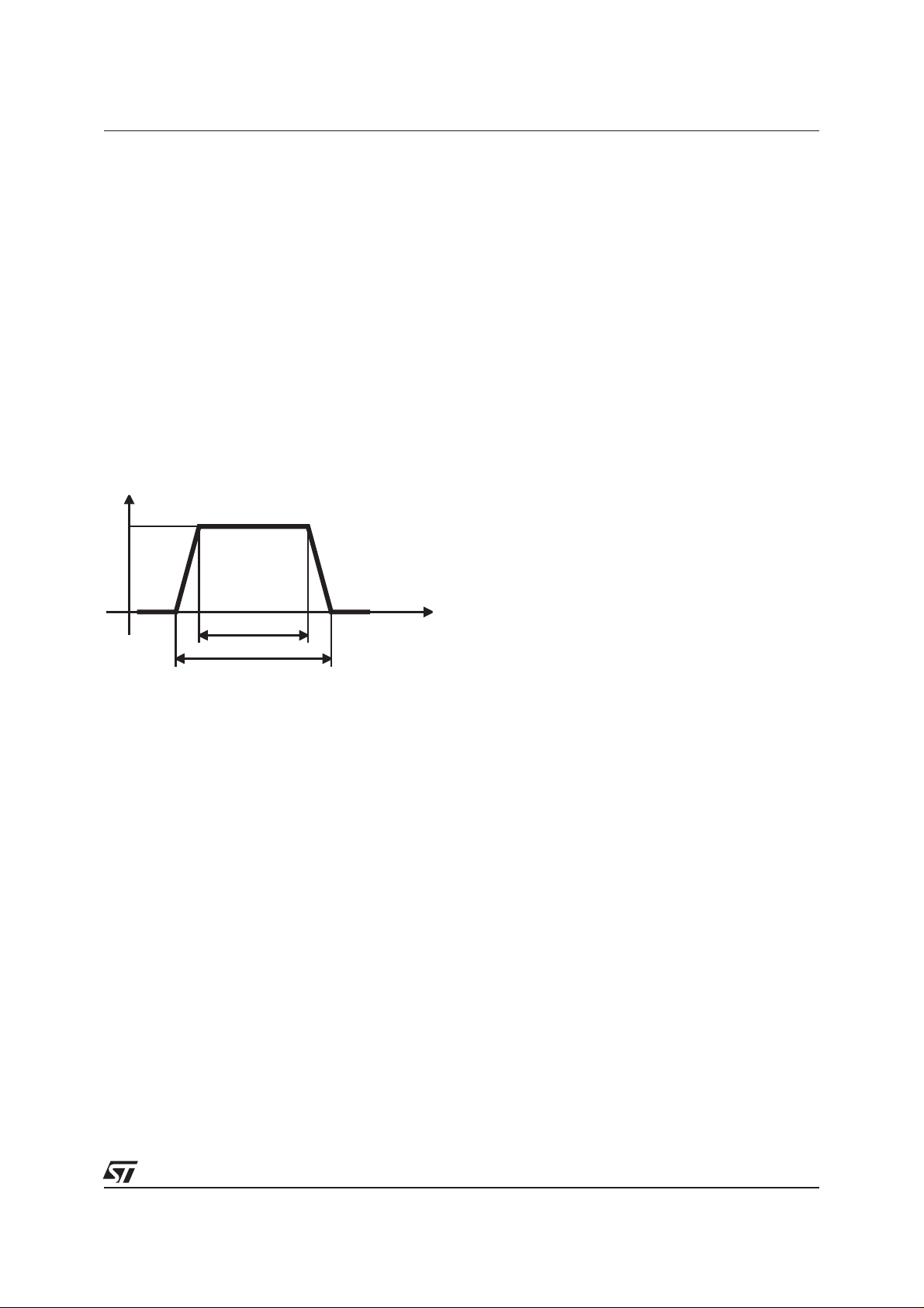
DYNAMIC RESISTANCE MEASUREMENT
The short duration of the ESD has led us to prefer
amore adapted test wave, as below defined, to the
classical 8/20µs and 10/1000µs surges.
I
Ipp
As the value of the dynamic resistance remains
stable for a surge duration lower than 20µs, the
.
2.5µs rectangular surge is well adapted. In
addition both rise and fall times are optimized to
avoid any parasitic phenomenon during the
measurement of Rd.
ESDAxxL
2µs
tp = 2.5µs
2.5µs duration measurement wave.
t
3/6