

®
HIGH VOLTAGE FAST-SWITCHING
■ HIGH VOLTAGE CAPABILITY
■ LOW SPREAD OF DYNAMIC PARAMETERS
■ MINIMUM LOT- TO- LO T SP RE AD F OR
RELIABLE OPERATION
■ VERY H IGH SWITCHING SPEED
■ FULLY CHARACTERIZE D AT 125
■ LARGE RBSOA
■ FULLY INSULATE D PA CKA GE (U. L.
COMPLIANT) FOR EASY MOUNTING
APPLICATIONS
■ HORIZONT A L DEFLE CT ION F OR TV
■ SMPS
■ ELECTRONIC BALLASTS FOR
FLUORESCENT LIGHTING
DESCRIPTION
The BUL312FP is manufactured using high
voltage Multi Epitaxial Planar technology for high
switching speeds and high voltage capability. It
uses a Cellular Emitter structure with planar edge
termination to enhance switching speeds while
maintaining a wide RBSOA.
o
C
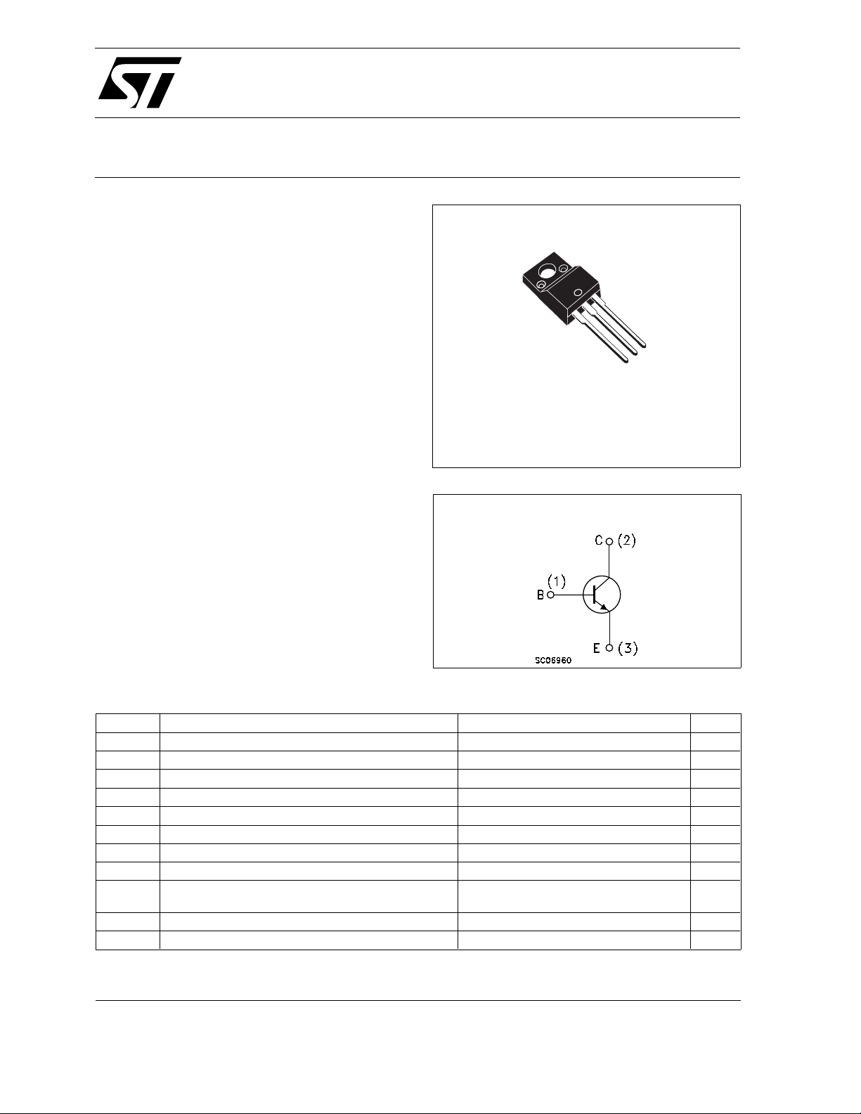
BUL312FP
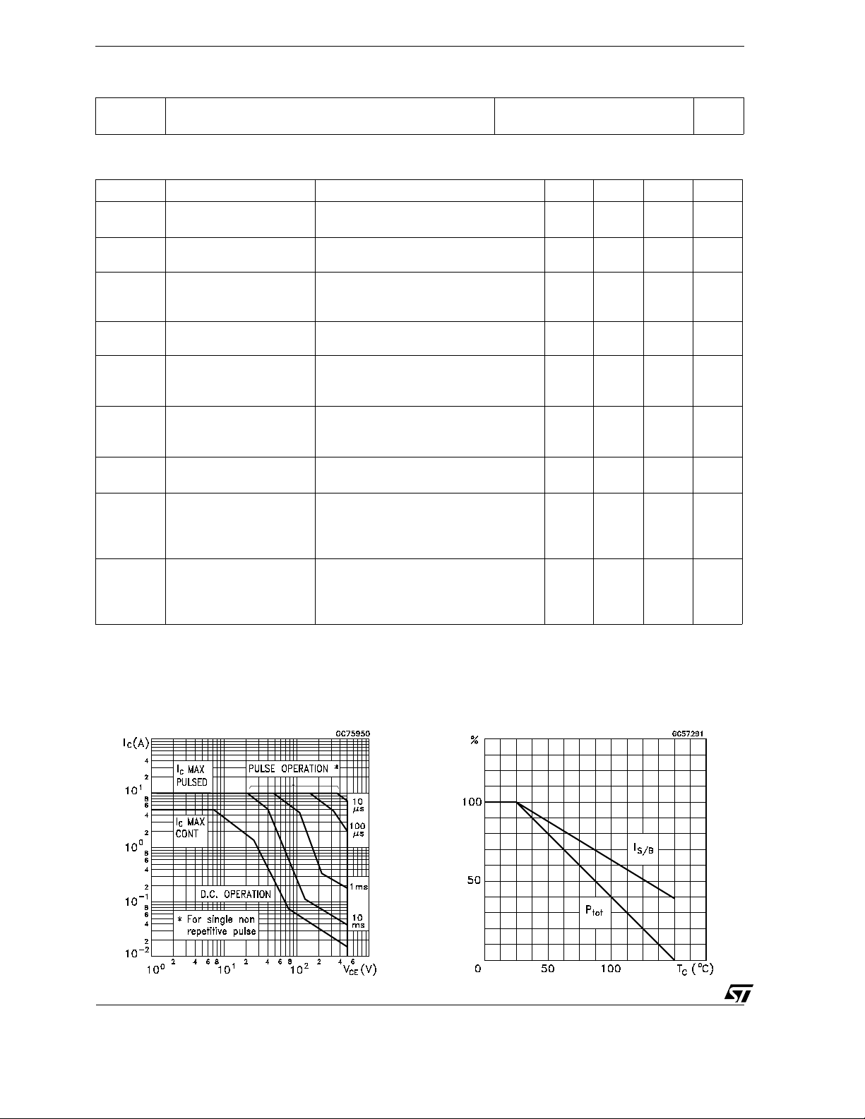
NPN POWER TRANSISTOR
3
2
1
TO-220FP
INTERNAL SCHEMATIC DIAGRAM
ABSOL UT E MAXIMU M RATINGS
Symbol Parameter Value Unit
V
V
V
I
I
P
V
T
March 2004
Collector-Emitter Voltage (VBE = 0) 1150 V
CES
Collector-Emitter Voltage (IB = 0) 500 V
CEO
Emitter-Base Voltage (IC = 0) 9 V
EBO
I
Collector Current 5 A
C
Collector Peak Current (tp <5 ms) 10 A
CM
Base Current 3 A
I
B
Base Peak Current (tp <5 ms) 4 A
BM
Total Dissipation at Tc = 25 oC36W
tot
Insulation Withstand Voltage (RMS) from All
isol
1500 V
Three Leads to External Heatsink
Storage Temperature -65 to 150
stg
Max. Operating Junction Temperature 150
T
j
o
C
o
C
1/6
BUL312FP
THERMAL DATA
R
thj-case
R
thj-amb
Thermal Resistance Junction-Case Max
Thermal Resistance Junction-Ambient Max
3.5
62.5
o
C/W
o
C/W
ELECTRICAL CHARACTERISTICS (T
= 25 oC unless otherwise specified)
case
Symbol Parameter Test Conditions Min. Typ. Max. Unit
I
CES
I
CEO
V
CEO(sus)
Collector Cut-off
Current (V
BE
= 0)
Collector Cut-off
Current (I
= 0)
B
∗ Collector-Emitter
= 1150 V
V
CE
V
= 1150 V Tj = 125 oC
CE
V
= 500 V 250 µA
CE
I
= 100 mA L= 25 mH 500 V
C
1
2
Sustaining Voltage
(I
= 0)
B
V
V
CE(sat)
EBO
Emitter-Base Voltage
= 0)
(I
C
∗ Collector-Emitter
Saturation Voltage
V
∗ Base-Emitter
BE(sat)
Saturation Voltage
h
∗ DC Current Gain IC = 10 mA VCE = 5 V
FE
INDUCTIVE LOAD
t
Storage Time
s
Fall Time
t
f
I
= 10 mA 10 V
E
IC = 1 A IB = 0.2 A
I
= 2 A IB = 0.4 A
C
I
= 3 A IB = 0.6 A
C
IC = 1 A IB = 0.2 A
I
= 2 A IB = 0.4 A
C
I
= 3 A IB = 0.6 A
C
0.5
0.7
1.1
1
1.1
1.2
8
I
= 3 A VCE = 2.5 V
C
I
= 2 A IB1 = 0.4 A
C
V
V
= -5 V R
BE(off)
= 250 V L = 200 µH
CL
BB
= 0 Ω
8 13.5
1.2
80
1.9
160
(see fig. 1)
INDUCTIVE LOAD
t
Storage Time
s
Fall Time
t
f
∗ Pulsed: Pulse duration = 300 µs, duty cycle 1.5 %
I
= 2 A IB1 = 0.4 A
C
V
V
T
= -5V R
BE(off)
= 250 V L = 200 µH
CL
= 125 oC (see fig. 1)
j
BB
= 0 Ω
1.8
150
mA
mA
V
V
V
V
V
V
µs
ns
µs
ns
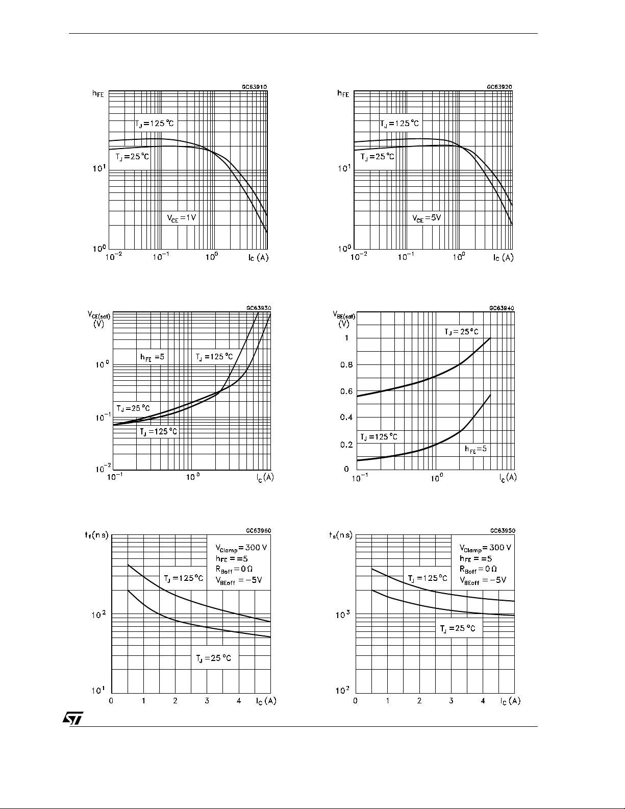
Safe Operating Areas Derating Curve
2/6
BUL312FP
DC Current Gain
Collector Emit ter Sat uration Volt ag e
DC Current Gain
Base Emitter Satur ation Voltage
Inductive Fall Time
Inductive Storage Time
3/6

BUL312FP
Reverse Biased SOA Figure 1: Inductive Load Switching Test
Circuit
(1) Fast electronic switch
(2) Non-inductive Resistor
(3) Fast recovery rectifie r
4/6

TO-220FP MECHANICAL DATA
BUL312FP
DIM.
MIN. TYP. MAX. MIN. TYP. MAX.
A 4.4 4.6 0.173 0.181
B 2.5 2.7 0.098 0.106
D 2.5 2.75 0.098 0.108
E 0.45 0.7 0.017 0.027
F 0.75 1 0.030 0.039
F1 1.15 1.7 0.045 0.067
F2 1.15 1.7 0.045 0.067
G 4.95 5.2 0.195 0.204
G1 2.4 2.7 0.094 0.106
H 1 0 10.4 0.393 0.409
L2 16 0.630
L3 28.6 30.6 1.126 1.204
L4 9.8 10.6 0.385 0.417
L6 15.9 16.4 0.626 0.645
L7 9 9.3 0.354 0.366
Ø 3 3.2 0.118 0.126
mm inch
A
B
H
E
D
L3
L6
L7
¯
F1
F
G1
G
F2
123
L2
L4
5/6

BUL312FP
Information furnished is believed to be accurate and reliable. However, STMicroelectronics assumes no responsibility for the consequences
of use of such inform ation nor for any infringe ment o f patents or other rig hts o f third par ties which ma y resul t from i ts use. N o li cen se is
granted by implicatio n or otherwise under any patent or patent rights of STMicroelectronics. Specification mentioned in this publication are
subject to change without notice. This publication supersedes and replaces all information previously supplied. STMicroelectronics products
are not authorized for use as critical compo nents in life support devices or systems without express written approval of STMicroelectronics.
The ST logo is a trademark of STMicroelectronics.
All other names are the property of their respective owners.
© 2004 STMicroelectronics – All Rights reserved
STMicroelectronics GROUP OF COMPANIES
Australia - Belgium - Brazil - Canada - China - Czech Republic - Finland - France - Germany - Hong Kong - India - Israel - Italy - Japan -
Malaysia - Malta - Morocco - Singapore - Spain - Sweden - Switzerland - United Kingdom - United States.
http://www.st.com
6/6

This datasheet has been download from:
www.datasheetcatalog.com
Datasheets for electronics components.
 Loading...