

BlueNRG-M0
Datasheet
Very low power network processor module for Bluetooth® low energy v4.2
Features
• Bluetooth v4.2 compliant
– Supports master and slave modes
– Multiple roles supported simultaneously
• Embedded Bluetooth low energy protocol stack
– GAP, GATT, SM, L2CAP, LL, RFPHY
• Bluetooth low energy profiles provided separately
• Embedded ST BlueNRG-MS network processor
– Up to +8 dBm available output power
– Down to -88 dBm Rx sensitivity
– Up to 96 dB link budget with excellent link reliability
• Host interface
– SPI, IRQ, and RESET
– On-field stack upgrading available via SPI
• AES security co-processor
• Certification
– CE qualified
– FCC, IC modular approval certified
– TYPE qualified
– BQE qualified
– WPC certification (BlueNRG-M0L)
Product status link
BlueNRG-M0
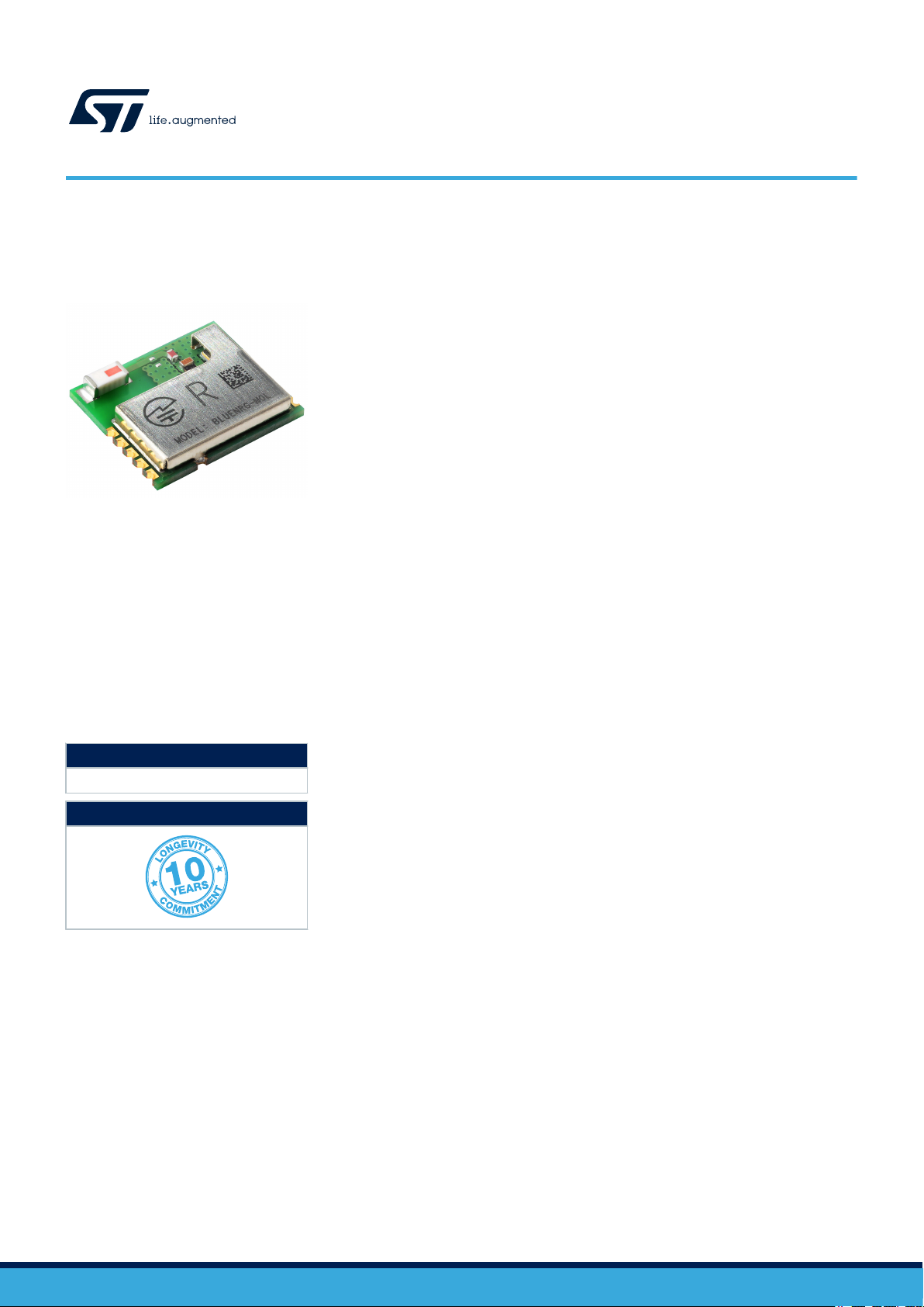
Product label
• On-board chip antenna
• Operating supply voltage: from 1.7 to 3.6 V
• Operating temperature range: -40 °C to 85 °C
Applications
• Watches
• Fitness, wellness and sports
• Consumer medical
• Security/proximity
• Remote control
• Home and industrial automation
• Assisted living
• Mobile phone peripherals
• PC peripherals
Description
The BlueNRG-M0 is an easy to use Bluetooth® low energy master/slave network
processor module, compliant with Bluetooth v4.2. The BlueNRG-M0 module supports
multiple roles simultaneously, and can act at the same time as Bluetooth low energy
sensor and hub device.
DS13023 - Rev 5 - March 2021
For further information contact your local STMicroelectronics sales office.
www.st.com

BlueNRG-M0
The entire Bluetooth low energy stack and protocols are embedded into BlueNRG-
M0 module. The external host application processor, where the application resides, is
connected to the BlueNRG-M0 module through a standard SPI interface.
The BlueNRG-M0 module provides a complete RF platform in a tiny form factor.
Radio, antenna, high frequency and LPO oscillators are integrated to offer a certified
solution to optimize the time-to-market of the final applications.
The BlueNRG-M0 can be powered directly with a standard 3 V coin cell battery, a
pair of AAA batteries or any power source from 1.7 to 3.6 V.
DS13023 - Rev 5
page 2/27

1 General description
The BlueNRG-M0 is a single-mode Bluetooth low energy master/slave network processor module compliant with
Bluetooth® v4.2.
The BlueNRG-M0 module has been designed around the ST BlueNRG-MS network processor, on which a
complete power-optimized stack for Bluetooth single mode protocol runs, providing
• Master, slave role support
• GAP: central, peripheral, observer or broadcaster roles
• ATT/GATT: client and server
• SM: privacy, authentication and authorization
• L2CAP
• Link Layer: AES-128 encryption and decryption
The BlueNRG-MS radio embeds non-volatile Flash memory allows on-field stack upgrading. In addition,
according to the Bluetooth specification v4.2, the BlueNRG-M0 module provides:
• Multiple roles simultaneously support
• Support simultaneous advertising and scanning
• Support being slave of up to two masters simultaneously
• Privacy V1.1
• Low duty cycle directed advertising
• Connection parameters request procedure
• LE Ping
• 32 bits UUIDs
• L2CAP connection oriented channels
The BlueNRG-M0 module is equipped with Bluetooth low energy profiles in C source code, available for the ST
radio BlueNRG-MS.
The external host application processor, where the application resides, is interfaced with the BlueNRG-M0 module
through an application controller interface protocol, which is based on a standard SPI interface.
The BlueNRG-M0 module enables wireless connectivity into electronic devices, not requiring any RF experience
or expertise for integration into the final product. The BlueNRG-M0 module provides a complete RF platform in a
tiny form factor and being a certified solution optimizes the time-to-market of the final applications.
The BlueNRG-M0 module allows applications to meet of the tight advisable peak current requirements imposed
with the use of standard coin cell batteries. Optimized results are obtained when the embedded high-efficiency
DC-DC step-down converter is used (BLUENRG-M0A). Instead, concerning the BLUENRG-M0L the best
performance in terms of power consumption is achieved using a 1.8V DC power supply.
The BlueNRG-M0 can be powered directly with a standard 3 V coin cell battery, a pair of AAA batteries or any
power source from 1.7 to 3.6 V.
ST may update the FW provided with the modules at any time. ST recommends that users regularly check for
documentation and the current FW version available at www.st.com/bluemodules.
BlueNRG-M0
General description
DS13023 - Rev 5
page 3/27
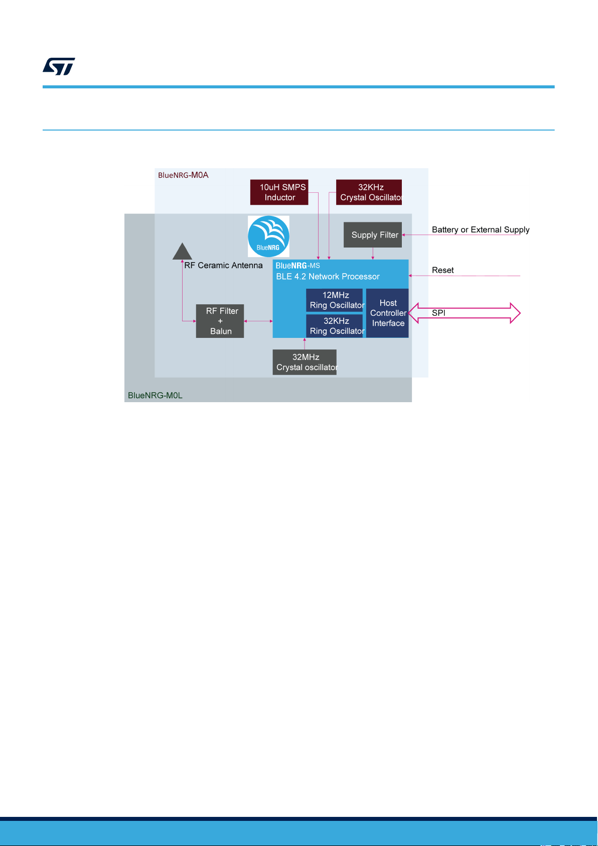
2 Block diagram
BlueNRG-M0
Block diagram
Figure 1. HW block diagram for the BlueNRG-M0
DS13023 - Rev 5
page 4/27
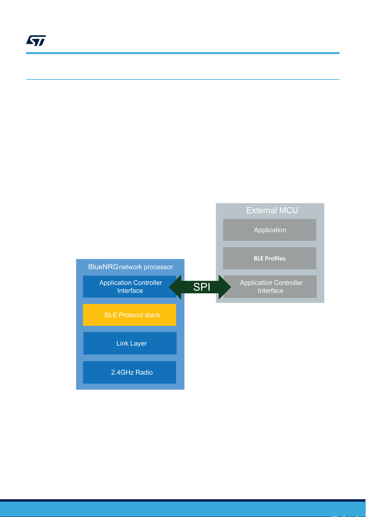
3 Software architecture
3.1 Bluetooth firmware implementation
The BlueNRG-M0 modules have been designed to work with an external host processor. The external host
application processor, where the application resides, is interfaced with the BlueNRG-MS inside the BlueNRG-M0
modules through an application controller interface (ACI) protocol, which is based on a standard SPI slave
interface as transport layer, basing on five physical wires:
• 2 control wires (Clock and “Chip Select")
• 2 data wires with serial shift-out (MOSI and MISO) in full duplex
• 1 wire to indicate data availability from the slave (IRQ)
All the SPI pins have an internal pull-down except for the CS that has a pull-up. All the SPI pins, except the CS,
are in high impedance state during the low-power states. The IRQ pin needs a pull-down external resistor.
Figure 2. BlueNRG-M0 application block diagram
BlueNRG-M0
Software architecture
DS13023 - Rev 5
page 5/27
4 General characteristics
4.1 Absolute maximum ratings
Ratings Min. Typ. Max. Unit
Storage temperature range -40 - +85 °C
Supply voltage, VIN -0.3 - 3.9 V
I/O pin Voltage (VIO five-volt tolerant pin) -0.3 - 3.9 V
RF saturation input power - 8 - dBm
VESD-HBM Electrostatic discharge voltage ±2.0 kV
4.2 Operating conditions
BlueNRG-M0
General characteristics
Table 1. Operating conditions
Ratings Min. Typ. Max. Unit
Storage temperature range -40 - +85 °C
Operating ambient temperature range -40 - +85 °C
Supply voltage, VIN 1.7 3.3 3.6 V
Signals & I/O pin voltage (according supply voltage) 1.7 - 3.6 V
Frequency range 2402 - 2480 MHz
DS13023 - Rev 5
page 6/27
5 Electrical specifications
5.1 Electrical characteristics
Characteristic measured over recommended operating conditions unless otherwise specified. Typical values are
referred to VIN= 3.3 V, 25 °C, SMPS on, XO 32 kHz and 32 MHz.
Table 2. Electrical characteristics for the BLUENRG-M0A
Symbol Parameter Test conditions Min. Typ. Max. Unit
Sleep mode: 32 kHz XO ON (12 KB retention
Sleep mode: 32 kHz XO ON (24 KB retention
IDD Supply current
BlueNRG-M0
Electrical specifications
Reset 5 nA
Standby 1.8 uA
RAM)
RAM)
Active mode 2.12 mA
RX 9.36 mA
TX +8 dBm 16.50 mA
TX +4 dBm 12.04 mA
TX +2 dBm 10.40 mA
TX -2 dBm 9.44 mA
TX -5 dBm 8.79 mA
TX -8 dBm 8.29 mA
TX -11 dBm 8.01 mA
TX -14 dBm 7.82 mA
1.7
μA
2.2
Characteristic measured over recommended operating condition unless otherwise specified. Typical values are
referred to VIN= 3.3 V, 25 °C, SMPS off, RO 32 kHz and 32 MHz.
Table 3. Electrical characteristics for the BLUENRG-M0L
Symbol
IDD Supply current
Parameter Test conditions Min. Typ. Max. Unit
Reset 5 nA
Standby 1.7 uA
Sleep mode: 32 kHz RO ON (12 kB retention
RAM)
Sleep mode: 32 kHz RO ON (24 kB retention
RAM)
Active mode 2.54 mA
RX 16.36 mA
TX +8 dBm 27.35 mA
TX +4 dBm 21.3 mA
TX +2 dBm 18.29 mA
TX -2 dBm 16.44 mA
2.8
μA
3.2
DS13023 - Rev 5
page 7/27
Symbol Parameter Test conditions Min. Typ. Max. Unit
IDD Supply current
5.2 Digital I/O specifications
IO pins are directly connected to the embedded state of the art BlueNRG-MS chipset. For more details about the
digital I/I specification, please refer directly to the BlueNRG-MS datasheet available on www.st.com.
5.3 RF general characteristics
Characteristic measured over recommended operating conditions unless otherwise specified. Typical value are
referred to VIN= 3.3 V, 25 °C, DC/DC on, XO 32 kHz (BLUENRG-M0A only) and XO 32 MHz.
BlueNRG-M0
Digital I/O specifications
TX -5 dBm 15.18 mA
TX -8 dBm 14.19 mA
TX -11 dBm 13.61 mA
TX -14 dBm 13.25 mA
Table 4. RF general characteristics
Symbol Parameter Test conditions Min. Typ. Max. Unit
FREQ Frequency range 2400 - 2483.5 MHz
FCH Channel spacing - 2 - MHz
RFch RF channel center frequency 2402 - 2480 MHz
Table 5. BLUENRG-M0A RF characteristics
Symbol Parameter Test conditions Min. Typ. Max. Unit
RPMAX
RXSENS
(1)
Output power
Sensitivity
(2)
(2)
Radiated +6 dBm
Conducted -85 dBm
1. PA-Level set to 0x07 and En-High_Power set to 0x01 (corresponding to +8 dBm in conducted mode).
2. Radiated power may be impacted by application board / housing / etc.
Table 6. BLUENRG-M0L RF characteristics
Symbol
(1)
RPMAX
RXSENS
Radiated output power
Sensitivity
1. PA-Level set to 0x07 and En-High_Power set to 0x01 (corresponding to +8dBm in conducted mode)
2. Radiated power may be impacted by application board / housing / etc.
Parameter Test conditions Min. Typ. Max. Unit
(2)
(2)
Radiated +6 dBm
Conducted -85 dBm
DS13023 - Rev 5
page 8/27
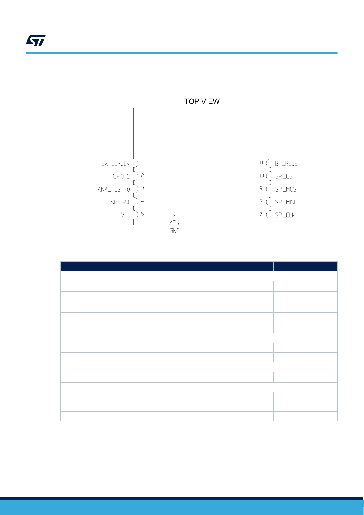
5.4 Pin assignment
BlueNRG-M0
Pin assignment
Figure 3. Pin connection
Table 7. Pin connection
Name
SPI_IRQ O 4 SPI IRQ (SLAVE has data for MASTER)
SPI_CLK I 7 SPI CLOCK (Max. 8 MHz)
SPI_MISO O 8 SPI MISO (MASTER in / SLAVE out)
SPI_MOSI I 9 SPI MOSI (MASTER out SLAVE in)
SPI_CS I 10 SPI “Chip select” (SPI slave select)
Vin 5 Vin (1.7 V - 3.6 V max.)
GND 6 GND
BT_RESET I 11
EXT_LPCLK I 1 Not connected
GPIO2 I/O 2 Not connected
ANA TEST 0 I 3 Not connected
Type Pin # Description V max. tolerant
SPI interface
Power and ground
Reset
Reset input (active low < 0.35 Vin)
LPO
(1.7 V - 3.6 V max.)
V
in
V
in
V
in
V
in
V
in
DS13023 - Rev 5
page 9/27

6 Hardware design
The BlueNRG-M0 module supports SPI hardware interfaces.
Note: • All unused pins should be left floating; do not ground
• All GND pins must be well grounded
• The area around the module should be free of any ground planes, power planes, trace routings, or metal
for 6 mm from the module antenna position, in all directions.
• Traces should not be routed underneath the module
BlueNRG-M0
Hardware design
6.1
Reflow soldering
The BlueNRG-M0 is a high temperature strength surface mount Bluetooth® module supplied on a 11-pin, 4-layer
PCB. The final assembly recommended reflow profiles are indicated here below.
Soldering phase has to be executed with care: in order to avoid undesired melting phenomenon, particular
attention has to be taken on the set up of the peak temperature.
Here are some suggestions for the temperature profile based on the following recommendations.
Table 8. Soldering profile
Profile feature PB-free assembly
Average ramp up rate (T
Preheat
temperature min (TS min.)
temperature max (TS max.)
time (tS min to tS max) (tS)
Time maintained above
Temperature T
Time t
L
Peak temperature (TP)
Time within 5 °C of peak temperature (TP -5°)
Ramp down rate 6 °C/s
Time from 25 °C to peak temperature 8 minutes max.
SMAX
L
to Tp)
3°C/ sec max
150 °C
200 °C
60-100 s
217 °C
60-70 s
240+0 °C
10-20 s
DS13023 - Rev 5
Figure 4. Soldering profiles
page 10/27

7 Regulatory compliance
7.1 FCC certification
This module has been tested and found to comply with the FCC part 15 rules. These limits are designed to
provide reasonable protection against harmful interference in approved installations. This equipment generates,
uses, and can radiate radio frequency energy and, if not installed and used in accordance with the instructions,
may cause harmful interference to radio communications.
However, there is no guarantee that interference may not occur in a particular installation.
This device complies with part 15 of the FCC rules. Operation is subject to the following two conditions:
1. this device may not cause harmfulinterference
2. this device must accept any interference received, including interference that may cause undesired
operation
Modifications or changes to this equipment not expressly approved by STMicroelectronics may render void the
user's authority to operate this equipment.
Modular approval
FCC ID: S9NBNRGM0AL
In accordance with FCC part 15, the BlueNRG-M0 is listed as a modular transmitter device.
This module is evaluated for stand-alone use only. Finished products incorporating multiple transmitters must
comply with collocation and RF exposure requirements in accordance with FCC multi-transmitter product
procedures. Collocated transmitters operating in portable RF Exposure conditions (e.g. <20 cm from persons
including but not limited to body worn and hand held devices) may require separate approval.
BlueNRG-M0
Regulatory compliance
7.1.1 Labeling instructions
When the BlueNRG-M0 is integrated into the final product, the OEM must ensure that the FCC labeling
requirements are satisfied. A statement must be included on the exterior of the final product which indicates
the product includes a certified module. The label should state the following (or similar wording that conveys the
same meaning):
Contains FCC ID: S9NBNRGM0AL
OR
This product contains FCC ID: S9NBNRGM0AL
The OEM must include the following statements on the exterior of the final product unless the product is too small
(e.g. less than 4 x 4 inches):
This device complies with part 15 of the FCC rules. Operation is subjected to the following two conditions:
1. this device may not cause harmful interference and
2. this device must accept any interference received, including any interference that may cause undesired
operations
7.1.2 Product manual instructions
This section applies to OEM final products containing the BlueNRG-M0 module, subjected to FCC compliance.
The final product manual must contain the following statement (or a similar statement that conveys the same
meaning):
Note: Changes or modifications not expressly approved by the party responsible for compliance could void the user's
authority to operate the equipment. (Part. 15.21)
In the case where an OEM seeks Class B (residential) limits for the final product, the following statement must be
included in the final product manual:
DS13023 - Rev 5
page 11/27

BlueNRG-M0
IC certification
Note: This equipment has been tested and found to comply with the limits for a Class B digital device, pursuant to part
15 of the FCC rules. These limits are designed to provide reasonable protection against harmful interference
in a residential installation. This equipment generates, uses and can radiate radio frequency energy and, if not
installed and used in accordance with the instructions, may cause harmful interference to radio communications.
However, there is no guarantee that interference will not occur in a particular installation. If this equipment does
cause harmful interference to radio or television reception, which can be determined by turning the equipment
off and on, the user is encouraged to try to correct the interference by one or more of the following measures:
• Reorient or relocate the receiving antenna
• Increase the separation between the equipment and receiver
• Connect the equipment into an outlet on a circuit different from that to which the receiver is connected
• Consult the dealer or an experienced radio/TV technician for help
In the case where an OEM seeks the lesser category of a Class A digital device for the final product, the following
statement must be included in the final product manual:
Note: This equipment has been tested and found to comply with the limits for a Class A digital device, pursuant to part
15 of the FCC rules. These limits are designed to provide reasonable protection against harmful interference
when the equipment is operated in a commercial environment. This equipment generates, uses, and can radiate
radio frequency energy and, if not installed and used in accordance with the instruction manual, may cause
harmful interference to radio communications. Operation of this equipment in a residential area is likely to cause
harmful interference in which case the user will be required to correct the interference at his expense.
7.2 IC certification
This device contains license-exempt transmitter(s)/receiver(s) that comply with innovation, science and economic
development Canada’s license-exempt RSS(s). Operation is subjected to the following two conditions:
1. this device may not cause interference
and
1. this device must accept any interference, including interference that may cause undesired operations of the
device.
In addition, in accordance with RSS-102 clause 2.6, the RF exposure compliance distance of the BlueNRG-M0 is
set equal to 15 mm.
Modular approval
IC: 8976C-BNRGM0AL
In accordance with IC RSS-247, the BlueNRG-M0 is listed as a modular transmitter device.
This module is evaluated for stand-alone use only. Finished products incorporating multiple transmitters
must comply with collocation and RF exposure requirements in accordance with IC multi-transmitter product
procedures. Collocated transmitters operating in portable RF Exposure conditions (e.g. <20 cm from persons
including but not limited to body worn and hand held devices) may require separate approval.
7.2.1 Labeling instructions
When the BlueNRG-M0 is integrated into the final product, the OEM must ensure that the IC labeling
requirements are satisfied. A statement must be included on the exterior of the final product which indicates
that the product includes a certified module. The label should state the following (or similar wording that conveys
the same meaning):
Contains IC: 8976C-BNRGM0AL
or
this product contains IC: 8976C-BNRGM0AL
The OEM must include the following statements on the exterior of the final product unless the product is too small
(e.g. less than 4 x 4 inches):
This device complies with RSS-247 of the IC rules. Operation is subjected to the following two conditions:
1. this device may not cause harmful interference, and
1. this device must accept any interference received, including any interference that may cause undesired
operation
DS13023 - Rev 5
page 12/27

BlueNRG-M0
CE certification
7.2.2 Product manual instructions
This section applies to OEM final products containing the BlueNRG-M0 module, subjected to FCC compliance.
The final product manual must contain the following statement (or a similar statement that conveys the same
meaning):
Note: Changes or modifications not expressly approved by the party responsible for compliance could void the user's
authority to operate the equipment. (RSS-247)
In the case where an OEM seeks Class B (residential) limits for the final product, the following statement must be
included in the final product manual:
Note: This equipment has been tested and found to comply with the limits for a Class B digital device, pursuant to to
RSS-247 of the IC rules. These limits are designed to provide reasonable protection against harmful interference
in a residential installation. This equipment generates, uses and can radiate radio frequency energy and, if not
installed and used in accordance with the instructions, may cause harmful interference to radio communications.
However, there is no guarantee that interference will not occur in a particular installation. If this equipment does
cause harmful interference to radio or television reception, which can be determined by turning the equipment
off and on, the user is encouraged to try to correct the interference by one or more of the following measures:
• Reorient or relocate the receiving antenna
• Increase the separation between the equipment and receiver
• Connect the equipment into an outlet on a circuit different from that to which the receiver is connected
• Consult the dealer or an experienced radio/TV technician for help
In the case where an OEM seeks the lesser category of a Class A digital device for the final product, the following
statement must be included in the final product manual:
Note: This equipment has been tested and found to comply with the limits for a Class A digital device, pursuant to
RSS-247 of the IC rules. These limits are designed to provide reasonable protection against harmful interference
when the equipment is operated in a commercial environment. This equipment generates, uses, and can radiate
radio frequency energy and, if not installed and used in accordance with the instruction manual, may cause
harmful interference to radio communications. Operation of this equipment in a residential area is likely to cause
harmful interference in which case the user will be required to correct the interference at his expense.
7.3
CE certification
The BlueNRG-M0 module has been certified according to the following certification rules:
• ETSI EN 300 328 V 2.1.1 (2016-11)
• ETSI EN 301 489-17 V3.1.1 (2017-02)
• ETSI EN 301 489-1 V2.1.1 (2017-02)
• EN 62368-1:2020/A11:2020
(4)
• EN 62311:2008
1. ETSI EN 300 328 V 2.1.1 (2016 11): “electromagnetic compatibility and radio spectrum Matters (ERM); Wideband
transmission systems; data transmission equipment operating in the 2.4 GHZ ISM band and using wideband modulation
techniques; harmonized EN covering essential requirements under article 3.2 of the R&TTE directive”.
2. ETSI EN 301 489-17 V 3.1.1 (2017 02): “electromagnetic compatibility and radio spectrum matters (ERM); electromagnetic
compatibility (EMC) standard for radio equipment and services; part 17: specific condition for 2.4 GHz wideband
transmission systems and 5 GHz high performance RLAN equipment”.
3. ETSI EN 301 489-1 V2.1.1 (2017 02): “electromagnetic compatibility and radio spectrum matters (ERM); electromagnetic
compatibility (EMC) standard for radio equipment and services; part 1: common technical requirements”.
4. EN 62368-1:2020/A11:2020: “Audio/video, information and communication technology equipment - Part 1: Safety
requirements”.
The module is provided by CE marking:
The module has obtained the RED certificate: No. 0051-RED-0097
The Certificate of Conformity is available / downloadable at the following web page: www.ST.com/product/bluenrgm0.
(1)
(2)
(3)
DS13023 - Rev 5
page 13/27

BlueNRG-M0
CE certification
The certified module production firmware release is: 7.X
For additional information please refer to: STMicroelectronics Via C. Olivetti 2, Agrate Brianza 20864 (ITALY).
DS13023 - Rev 5
page 14/27

7.4 TYPE certification
The BlueNRG-M0 module has been tested according to following TYPE certification rules:
• Type of specified radio equipment
– Radio equipment according to certification ordinance article 2-1-9
• Sophisticated low power radio data communication system in 2.4 GHz band.
• Class of emissions, assigned frequency, and antenna power
– F1D 2402 - 2480 MHz channel separation 2 MHz/40 channel, 0.005 W
• Certification number:
– 006-000713 (BLUENRG-M0A)
– 006-000714 (BLUENRG-M0L)
7.5 WPC ETA certificate
The BlueNRG-M0L module is registered for equipment type approval (ETA) with WPC India.
• Registration No: ETA-SD-20201108376
7.6 Bluetooth certification
The module with embedded stack and profile has been qualified in accordance with SIG qualification rules:
• Declaration ID: D043964
• Qualified design ID: 122868
• Product type: End Product
• Core spec version: 4.2
• Product description: Bluetooth low energy v4.2 module
BlueNRG-M0
TYPE certification
DS13023 - Rev 5
page 15/27

8 Package information
In order to meet environmental requirements, ST offers these devices in different grades of ECOPACK packages,
depending on their level of environmental compliance. ECOPACK specifications, grade definitions and product
status are available at: www.st.com. ECOPACK is an ST trademark.
8.1 BlueNRG-M0 package information
Figure 5. BlueNRG-M0 package outline
BlueNRG-M0
Package information
DS13023 - Rev 5
page 16/27

Table 9. BlueNRG-M0 mechanical data
BlueNRG-M0
BlueNRG-M0 package information
Symbol
A
A1 0.7 0.8 0.9
A2 1.4 1.5 1.6
D 11.5
E 13.5
F 1
G 4.0
dia 0.7
Pad size X,Y (on bottom side) 0.6x1
e-pitch 1.27 tol.+/-0.025
Min. Typ. Max.
2.1 2.3 2.5
mm
Figure 6. BlueNRG-M0 recommended footprint
DS13023 - Rev 5
page 17/27

8.2 BlueNRG-M0 packing information
Figure 7. BlueNRG-M0 tape outline
Figure 8. BlueNRG-M0 tape dimension outline
BlueNRG-M0
BlueNRG-M0 packing information
DS13023 - Rev 5
page 18/27

Figure 9. BlueNRG-M0 reel outline
BlueNRG-M0
BlueNRG-M0 packing information
Table 10. BlueNRG-M0 reel mechanical data
Dimensions
A
B 1.5
C 12.8 13.5
D 20.2
G 24.4 26.4
N 100 103
T 26.4 30.4
Min. Max.
328 332
Reel
DS13023 - Rev 5
page 19/27

9 Ordering information
Order code Description MOQ Packing
BLUENRG-M0A
BLUENRG-M0L
Bluetooth® v4.2 low energy
Table 11. Ordering information
module
1000 pieces Tape and reel
BlueNRG-M0
Ordering information
DS13023 - Rev 5
page 20/27

10 Traceability
Each module is univocally identified by serial number stored in a 2D data matrix laser marked on the top side
(shield) of the module itself.
Each module bulk is identified by a bulk ID.
Bulk ID and module 2D data matrix are linked by a reciprocal traceability link. The module 2D data matrix traces
the lot number of any raw material used according to following rules:
Letter Meaning
HA Reserved
YWW Year and week number
E Reserved
LL Lot sequence number
XX Lot sub-sequence number
0000 Serial number
BlueNRG-M0
Traceability
Table 12. Traceability information
DS13023 - Rev 5
page 21/27

Revision history
Table 13. Document revision history
Date Version Changes
29-May-2019 1 Initial release.
Added logo to cover page.
23-Jul-2019 2
13-Mar-2020 3 Updated Figure 1. HW block diagram for the BlueNRG-M0.
13-Jan-2021 4
04-Mar-2021 5
Updated features in cover page, Table 5. BLUENRG-M0A RF characteristics
and Table 6. BLUENRG-M0L RF characteristics.
Added Section 8.2 BlueNRG-M0 packing information.
Updated cover image.
Updated Table 8. Soldering profile.
Updated Section 7.3 CE certification
Updated Section Features.
Added Section 7.5 WPC ETA certificate.
BlueNRG-M0
DS13023 - Rev 5
page 22/27

BlueNRG-M0
Contents
Contents
1 General description................................................................3
2 Block diagram .....................................................................4
3 Software architecture ..............................................................5
3.1 Bluetooth firmware implementation................................................5
4 General characteristics ............................................................6
4.1 Absolute maximum ratings.......................................................6
4.2 Operating conditions............................................................6
5 Electrical specifications ...........................................................7
5.1 Electrical characteristics.........................................................7
5.2 Digital I/O specifications .........................................................8
5.3 RF general characteristics .......................................................8
5.4 Pin assignment ................................................................9
6 Hardware design .................................................................10
6.1 Reflow soldering ..............................................................10
7 Regulatory compliance ...........................................................11
7.1 FCC certification ..............................................................11
7.1.1 Labeling instructions .....................................................11
7.1.2 Product manual instructions ............................................... 11
7.2 IC certification ................................................................12
7.2.1 Labeling instructions .....................................................12
7.2.2 Product manual instructions ...............................................13
7.3 CE certification ...............................................................13
7.4 TYPE certification .............................................................15
7.5 WPC ETA certificate ...........................................................15
7.6 Bluetooth certification ..........................................................15
8 Package information..............................................................16
8.1 BlueNRG-M0 package information ...............................................16
8.2 BlueNRG-M0 packing information................................................18
9 Ordering information .............................................................20
DS13023 - Rev 5
page 23/27

BlueNRG-M0
Contents
10 Traceability .......................................................................21
Revision history .......................................................................22
DS13023 - Rev 5
page 24/27

BlueNRG-M0
List of tables
List of tables
Table 1. Operating conditions ................................................................. 6
Table 2. Electrical characteristics for the BLUENRG-M0A ..............................................7
Table 3. Electrical characteristics for the BLUENRG-M0L ..............................................7
Table 4. RF general characteristics..............................................................8
Table 5. BLUENRG-M0A RF characteristics .......................................................8
Table 6. BLUENRG-M0L RF characteristics........................................................8
Table 7. Pin connection......................................................................9
Table 8. Soldering profile.................................................................... 10
Table 9. BlueNRG-M0 mechanical data.......................................................... 17
Table 10. BlueNRG-M0 reel mechanical data ...................................................... 19
Table 11. Ordering information................................................................. 20
Table 12. Traceability information............................................................... 21
Table 13. Document revision history ............................................................. 22
DS13023 - Rev 5
page 25/27

BlueNRG-M0
List of figures
List of figures
Figure 1. HW block diagram for the BlueNRG-M0 ...................................................4
Figure 2. BlueNRG-M0 application block diagram ...................................................5
Figure 3. Pin connection ....................................................................9
Figure 4. Soldering profiles ................................................................. 10
Figure 5. BlueNRG-M0 package outline ........................................................ 16
Figure 6. BlueNRG-M0 recommended footprint ................................................... 17
Figure 7. BlueNRG-M0 tape outline ........................................................... 18
Figure 8. BlueNRG-M0 tape dimension outline .................................................... 18
Figure 9. BlueNRG-M0 reel outline ............................................................19
DS13023 - Rev 5
page 26/27

BlueNRG-M0
IMPORTANT NOTICE – PLEASE READ CAREFULLY
STMicroelectronics NV and its subsidiaries (“ST”) reserve the right to make changes, corrections, enhancements, modifications, and improvements to ST
products and/or to this document at any time without notice. Purchasers should obtain the latest relevant information on ST products before placing orders. ST
products are sold pursuant to ST’s terms and conditions of sale in place at the time of order acknowledgement.
Purchasers are solely responsible for the choice, selection, and use of ST products and ST assumes no liability for application assistance or the design of
Purchasers’ products.
No license, express or implied, to any intellectual property right is granted by ST herein.
Resale of ST products with provisions different from the information set forth herein shall void any warranty granted by ST for such product.
ST and the ST logo are trademarks of ST. For additional information about ST trademarks, please refer to www.st.com/trademarks. All other product or service
names are the property of their respective owners.
Information in this document supersedes and replaces information previously supplied in any prior versions of this document.
© 2021 STMicroelectronics – All rights reserved
DS13023 - Rev 5
page 27/27
 Loading...