


UM2071
User manual
BlueNRG-1, BlueNRG-2 development kits
Introduction
The BlueNRG-1 and BlueNRG-2 devices are low power Bluetooth Low Energy (BLE) systems-on-chip that are compliant with
the Bluetooth® specification and support master, slave and simultaneous master-and-slave roles. BlueNRG-2 also supports the
Bluetooth Low Energy data length extension feature.
The following BlueNRG-1, BlueNRG-2 kits are available:
(1)
1. BlueNRG-1 development platforms (order code: STEVAL-IDB007V1
2. BlueNRG-2 development platforms (order code: STEVAL-IDB008V1
IDB008V1M)
1. This board is no longer available for purchase
The development platforms feature hardware resources for a wide range of application scenarios: sensor data (accelerometer,
pressure and temperature sensor), remote control interfaces (buttons and LEDs) and debug message management through
USB virtual COM. Three power options are available (USB only, battery only and external power supply plus USB) for high
application development and testing flexibility.
STEVAL-IDB007V2)
,
(1)
, STEVAL-IDB008V2, STEVAL-IDB009V1, STEVAL-
RELATED LINKS
The document content is also valid for the BlueNRG-1 STEVAL-IDB007V1M evaluation platform based on the SPBTLE-1S module with 32
MHz HS crystal.
UM2071 - Rev 12 - June 2020
For further information contact your local STMicroelectronics sales office.
www.st.com
1 Development platforms
UM2071
Development platforms
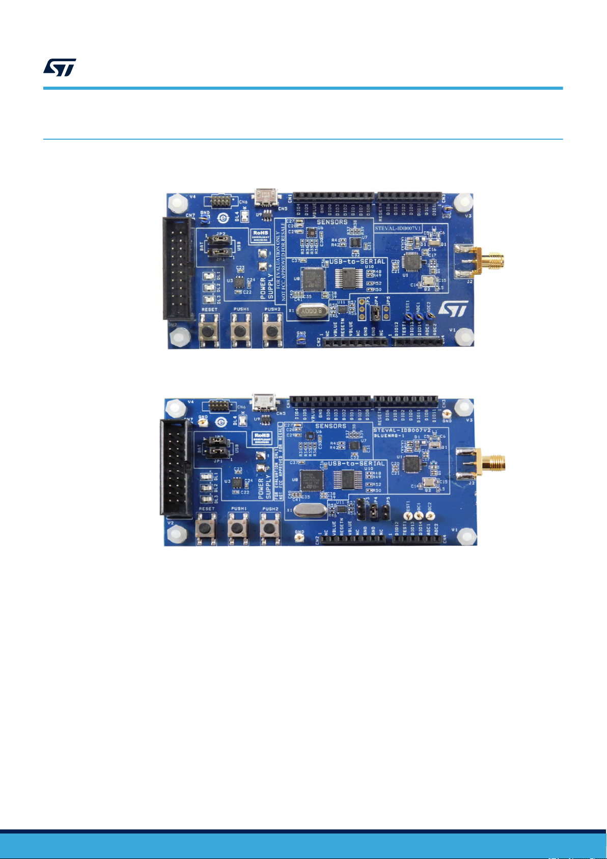
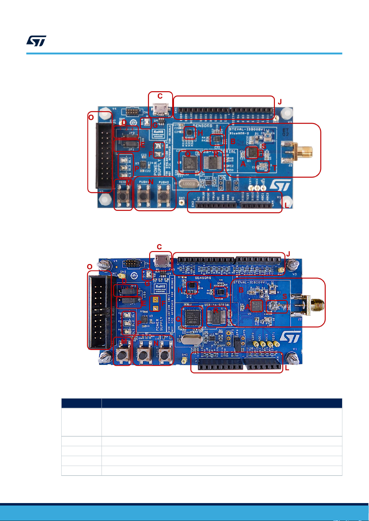
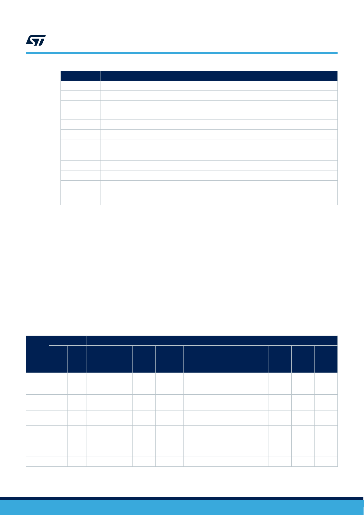
Figure 1. STEV
This item is no longer available for sale
Figure 2. STEV
based on BlueNRG-1 SoC
AL-IDB007V1 development platform
AL-IDB007V2 development platform
UM2071 - Rev 12
page 2/94
UM2071
Development platforms
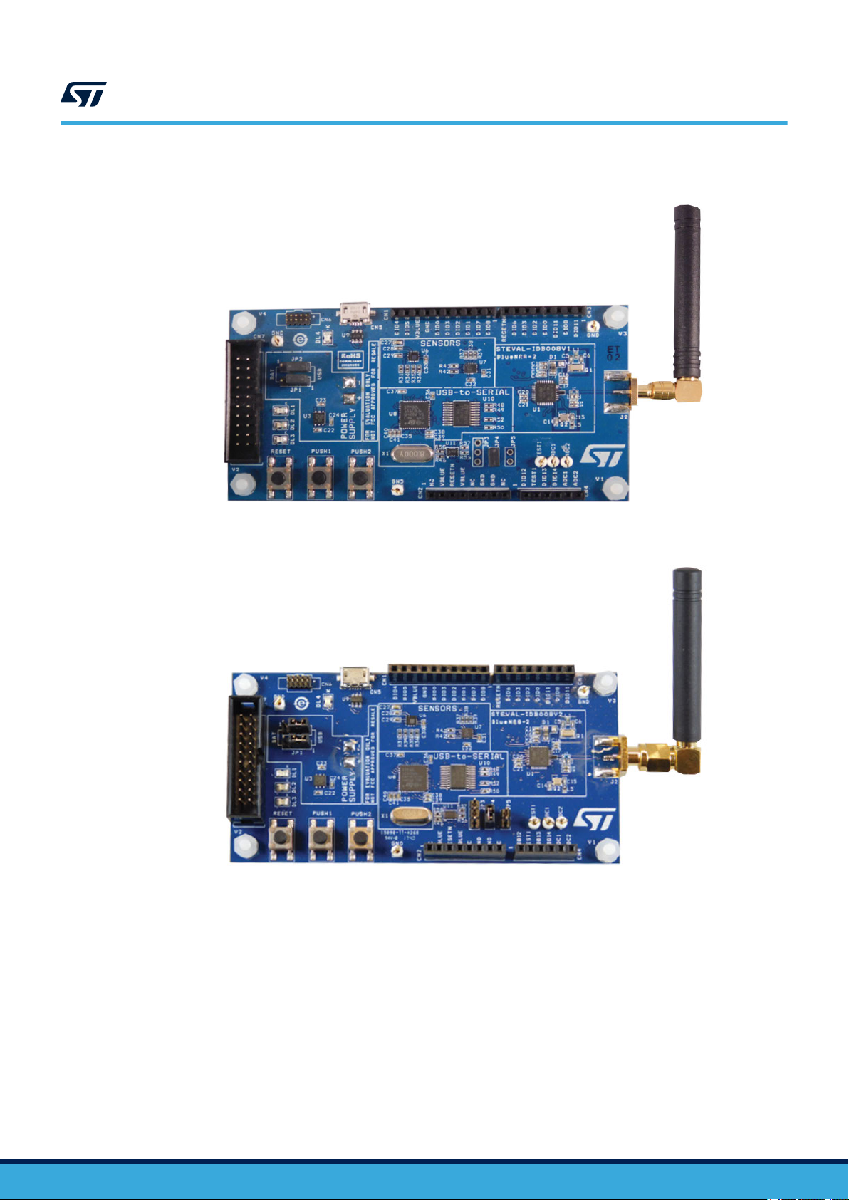
based on BlueNRG-2 SoC
based on BlueNRG-2 SoC
Figure 3. STEV
AL-IDB008V1 development platform
Figure 4. STEVAL-IDB008V2 development platform
UM2071 - Rev 12
page 3/94
UM2071
Development platforms
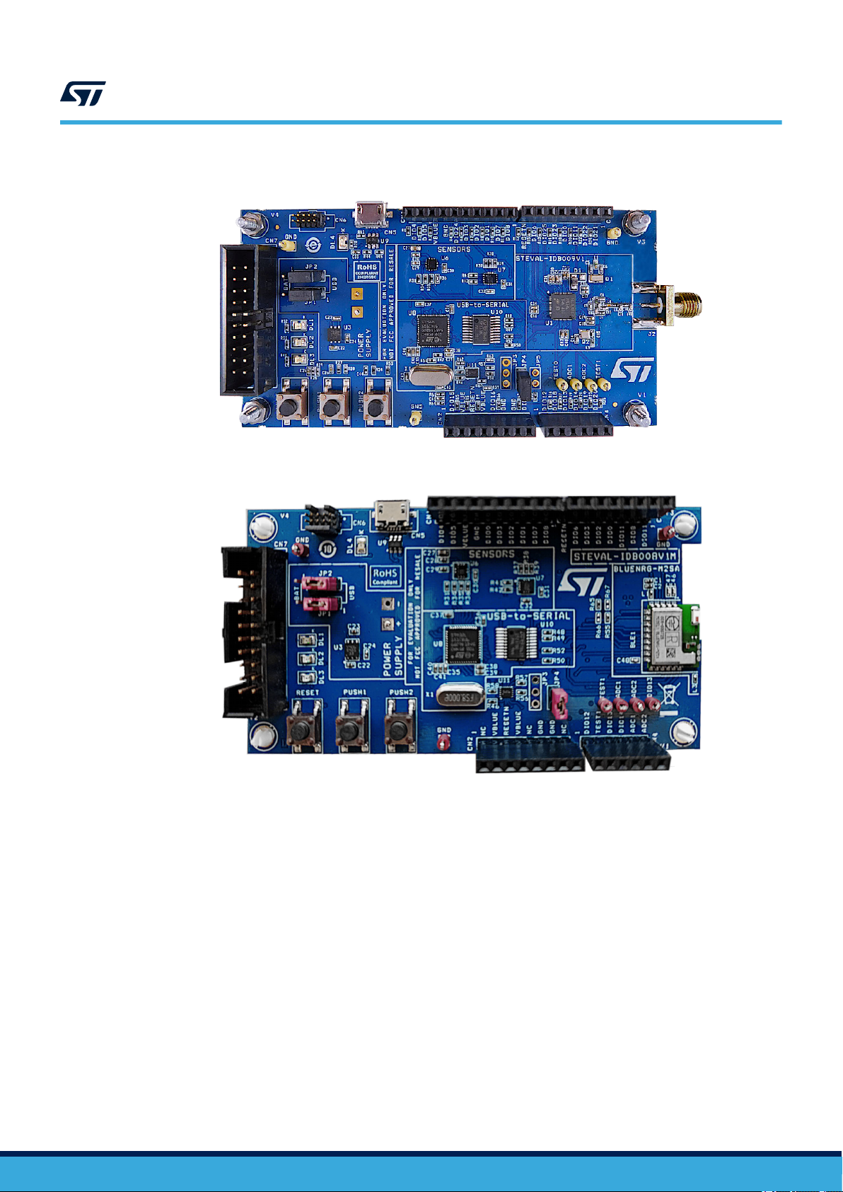
Figure 5. STEV
based on BlueNRG-2 SoC in QFN48 package
AL-IDB009V1 development platform
Figure 6. STEVAL-IDB008V1M development platform
based on BlueNRG-M2SA module with embedded BlueNRG-2 SoC
UM2071 - Rev 12
page 4/94

2 Getting started
2.1 Kit contents
The STEVAL-IDB007Vx/STEVAL-IDB008Vx kits include respectively:
a
•
BlueNRG-132 (QFN32 package)/BlueNRG-232 (QFN32 package) development platform
a 2.4 GHz Bluetooth antenna
•
• a USB cable
The STEVAL-IDB009Vx kit includes:
• a BlueNRG-248 (QFN48 package) development platform
• a 2.4 GHz Bluetooth antenna
• a USB cable
The STEVAL-IDB008V1M kit includes:
• a BlueNRG-M2SA certified module based on the BlueNRG-2 Bluetooth low energy system-on-chip
• a USB cable
UM2071
Getting started
2.2 System requirements
The BlueNRG-1, BlueNRG-2 Navigator and Radio Init Parameters Wizard PC applications require:
•
PC with Intel® or AMD® processor running Windows 7/10
• At least 128 MB of RAM
• USB ports
• At least 40 MB of available hard disk space
• Adobe Acrobat Reader 6.0 or later
2.3 BlueNRG-1_2 development kit setup
The following BlueNRG-1, BlueNRG-2 DK software packages are available: BlueNRG-1_2 DK SW package for
BlueNRG-1, BlueNRG-2 BLE stack v2.x family (STSW
After downloading the selected software package (STSW
bluenrg1-dk.zip contents to a temporary directory, launch BlueNRG-1_2-DK-x.x.x-Setup.exe and follow the onscreen instructions.
Note: EWARM Compiler 8.40.1 or later, Keil MDK-ARM v5.27 or later and Atollic-True Studio v8.1.0 are required for
building the related BlueNRG1_2_DK_x.x.x demonstration applications.
-BLUENRG1-DK).
-BLUENRG1-DK) from www.st.com, extract en.stsw-
UM2071 - Rev 12
page 5/94
Hardware description
3 Hardware description
3.1 STEVAL-IDB007Vx/STEVAL-IDB008Vx/STEVAL-IDB009Vx board overview
UM2071
The BlueNRG-1/BlueNRG-2
development kits lets you experiment with BlueNRG-1/BlueNRG-2 system on chip functions. They feature:
• Bluetooth® Low Energy (BLE) board based on the BlueNRG-1/BlueNRG-2 Bluetooth low energy system on
chip
• Associated development kit SW package including firmware and documentation
• Up to +8 dBm available output power (at antenna connector)
• Excellent receiver sensitivity (-88 dBm)
• Very low power consumption: 7.7 mA RX and 8.3 mA TX at -2 dBm
• Bluetooth® low energy compliant, supports master, slave and simultaneous master-and-slave roles
• Integrated balun which integrates a matching network and harmonics filter (only on STEVAL-IDB007Vx/
STEVAL-IDB008Vx)
• Discrete matching network on STEVAL-IDB009V1
• BlueNRG-M2SA certified module based on the BlueNRG-2 Bluetooth LE SoC on STEVAL-IDB008V1M
• SMA connector for antenna or measuring equipment (not available on STEVAL-IDB007V1M/8V1M)
• 3 user LEDs
• 2 user buttons
• 3D digital accelerometer and 3D digital gyroscope
• MEMS pressure sensor with embedded temperature sensor
• Battery holder
• JTAG debug connector
• USB to serial bridge for providing I/O channel with the BlueNRG-1/BlueNRG-2 device
• Jumper for measuring current for BlueNRG-1/BlueNRG-2 only
• RoHS compliant
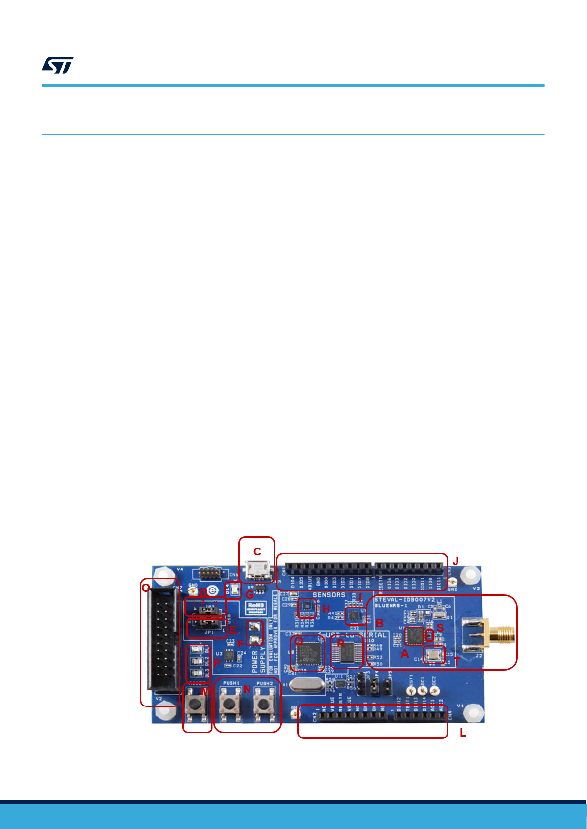
The following figure and table describe physical sections of the board.
devices in the STEV
AL-IDB007Vx/STEV
AL-IDB008Vx/STEVAL-IDB009Vx
Figure 7. STEVAL-IDB007Vx board components
UM2071 - Rev 12
page 6/94
UM2071
STEVAL-IDB007Vx/STEVAL-IDB008Vx/STEVAL-IDB009Vx board overview
Figure 8. STEV
Figure 9. STEV
AL-IDB008Vx board components
AL-IDB009V1 board components
UM2071 - Rev 12
Table 1. STEVAL-IDB007Vx/STEVAL-IDB008Vx/STEVAL-IDB009Vx board component descriptions
Region Description
BlueNRG-132 SoC on STEVAL-IDB007Vx
(1)
A
C
O JTAG connector
M RESET button
N Two USER buttons
BlueNRG-232 SoC on STEVAL-IDB008Vx
BlueNRG-248 SoC on STEVAL-IDB009Vx
Micro USB connector for power supply and I/O
page 7/94
Region Description
H LPS25HB MEMS pressure sensor with embedded temperature
I LSM6DS3 3D digital accelerometer and 3D digital gyroscope
G
P
PWR LED
Three user LEDs
Back of the PCB Battery holder for two AAA batteries
J, L Two rows of Arduino-compliant connectors
Integrated balun with matching network and harmonics filter (BALF-NRG-01D3 on STEV
S
AL-IDB008V1
STEV
and BALF-NRG-02D3 on STEVAL-IDB007V2/STEVAL-IDB008V2). Discrete matching
network on STEVAL-IDB009V1.
Q
STM32L151CBU6 48-pin microcontroller (USB to serial bridge for I/O channel to PC communication)
R ST2378E level translator to adapt voltage level between STM32 and BlueNRG-1
16 MHz High Speed Crystal on STEVAL-IDB007Vx
T
32 MHz High Speed Crystal on STEVAL-IDB008Vx, STEVAL-IDB009Vx, STEV
IDB007V1M/8V1M
1.On STEVAL-IDB008V1M, region A contains the BlueNRG-M2SA module
On STEVAL-IDB007V1M, region A contains the SPBTLE-1S module
2. STM32 is not intended to be programmed by users
UM2071
BlueNRG-1, BlueNRG-2 SoC connections
AL-IDB007V1/
(2)
AL-IDB009Vx, STEVAL-
3.2 BlueNRG-1, BlueNRG-2 SoC connections
The BlueNRG-132, BlueNRG-232 very low power Bluetooth low energy (BLE) single-mode system on chip
(Figure 7. STEVAL-IDB007Vx board components – region A /Figure 8. STEV
region A) have respectively 160 KB, 256 KB of Flash, 24 KB of RAM, a 32-bit core ARM Cortex-M0 processor and
several peripherals (ADC, 15 GPIOs, I²C, SPI, Timers, UART, WDG and RTC).
The BlueNRG-248 very low power Bluetooth low energy (BLE) single-mode system on chip has 256 KB of Flash,
24 KB of RAM, a 32-bit core ARM cortex-M0 processor and several peripherals (ADC, 26 GPIOs, I²C, SPI,
Timers, UART, WDG and RTC).
The microcontroller is connected to various components such as buttons, LEDs and sensors. The following table
describes the microcontroller pin functions.
Table 2. BlueNRG-1, BlueNRG-2 pins description with board functions
Pin no. Board function
Pin
name
QFN3
2
QFN4
(1)
8
LEDs Micro Buttons
(2)
DIO10 1 46
DIO9 2 47
DIO8 3 4
DIO7 4
5 DL2
DIO6 5 5 DL1
VBAT3 6 40
TXD
(P
A2)
Pressure
sensor
3D
accelerometer
and
gyroscope
AL-IDB008Vx board components -
JTAG CN1 CN2 CN3 CN4
JTMSSWTDI
O
JTCKSWTCK
pin 1
(IO8)
pin 2
(IO9)
pin 2
(TX)
pin 7
(IO6)
pin 6
(SCL)
pin 5
(SDA)
UM2071 - Rev 12
page 8/94

Pin no. Board function
Pin
name
QFN3
(1)
2
QFN4
(2)
8
LEDs Micro Buttons
Pressure
sensor
3D
accelerometer
and
gyroscope
SDA
DIO5 7 9
(PUSH2
button)
DIO4 8 13 SCL
DIO3 9 14 SDO/SA0
DIO2 10 15 SDA
DIO1 11 16 CS
DIO0 12 18 SCL
DIO14/
ANA
TEST013 21/23
DL3
UM2071
BlueNRG-1, BlueNRG-2 SoC connections
JTAG CN1 CN2 CN3 CN4
pin 9
(SDA)
pin 10
(SCL)
JTAGTDO
JTAGTDI
pin 5
(MISO)
pin 4
(MOSI)
pin 3
(CS)
pin 6
(SCK)
pin 6
(IO5)
pin 5
(IO4)
pin 4
(IO3)
pin 4
(AD3)
ANATES
T1
14 24
ADC1 15 25
ADC2 16 26
FXTAL1 17 27
FXTAL0 18 28
VBAT2 19 29
RF1 20 30
RF0 21 31
SXTAL1 22 33
SXTAL0 23 34
VBAT1 24 35
RESET 25 36 RESET RESET RESET
SMPSFI
L
T1
SMPSFI
LT2
VDD1V2
26 37
27 38
28 39
DIO13 29 41 PUSH1
DIO12 30 42 INT1
FTEST 31 43
DIO11 32 44
RXD
(P
A3)
pin 3
(NRST)
pin 8
(IO7)
pin 1
(RX)
pin 3
(IO2)
pin 3
(AD2)
pin 1
(AD0)
pin 2
(AD1)
UM2071 - Rev 12
page 9/94

Pin no. Board function
Pin
name
DIO15 - 20
DIO16 - 19
DIO17 - 17
DIO18 - 12
DIO19 - 11
DIO20 - 10
DIO21 - 6
DIO22 - 3
DIO23 - 2
DIO24 - 1
VBAT4 - 8/22
DIO25 - 48
QFN3
2
QFN4
(1)
(2)
8
LEDs Micro Buttons
Pressure
sensor
3D
accelerometer
and
gyroscope
UM2071
Power supply
JTAG CN1 CN2 CN3 CN4
1. QFN32 package on STEVAL-IDB007Vx and STEV
2. QFN48 package on STEVAL-IDB009Vx kits.
The board section labeled respectively BlueNRG-1, BlueNRG-2 (Figure 7. STEVAL-IDB007Vx board
components, Figure 8. STEV
AL-IDB008Vx board components, Figure 9. STEVAL-IDB009V1 board components –
region B) includes the following main components:
• BlueNRG-1/BlueNRG-2 low power system on chip (in a QFN32 package for STEVAL-IDB007Vx, STEVALIDB008Vx, QFN48 package for STEVAL-IDB009Vx) )
• BlueNRG-M2SA certified module based on the BlueNRG-2 Bluetooth LE SoC on STEVAL-IDB008V1M
• High frequency 16 MHz crystal on STEVAL-IDB007Vx and 32 MHz crystal on STEVAL-IDB008Vx, STEVALIDB009Vx
• Low frequency 32 kHz crystal for the lowest power consumption
• Integrated balun which integrates a matching network and harmonics filter
• SMA connector (not available on STEVAL-IDB007V1M/8V1M)
3.3 Power supply
Green LED DL4 (Figure 7.
components, Figure 9. STEVAL-IDB009V1 board components – region G) signals the board is being powered,
either via:
• micro USB connector CN5 (Figure 7. STEVAL-IDB007Vx board components, Figure 8. STEVAL-IDB008Vx
board components, Figure 9. STEVAL-IDB009V1 board components – region C)
• two AAA batteries (region F)
• an external DC power supply plus micro USB connector
The following table describes the power supply modes available on the STEVAL-IDB007V1, STEVAL-IDB008V1
boards and corresponding jumper settings.
STEVAL-IDB007Vx board components, Figure 8.
AL-IDB008Vx kits.
STEVAL-IDB008Vx board
UM2071 - Rev 12
Table 3. STEVAL-IDB007Vx, STEVAL-IDB008Vx, STEVAL-IDB009Vx kit platform power supply modes
Power supply mode JP1 JP2 Comment
1 - USB Fitted: 1-2 Fitted: 2-3
USB supply through connector CN5 (Figure 7. STEV
components, Figure 8. STEV
Figure 9. STEVAL-IDB009V1 board components – region C)
AL-IDB008Vx board components,
AL-IDB007Vx board
page 10/94
Power supply mode JP1 JP2 Comment
2 - Battery Fitted: 2-3 Fitted: 1-2 The supply voltage must be provided through battery pins (region F).
3 - Combo Fitted: 1-2 Optional
3.4 Jumpers
The available jumpers are listed in the table below.
UM2071
Jumpers
USB supply through connector CN5 for STM32L1; JP2 pin 2 external power for
BlueNRG-1, BlueNRG-2
able 4. STEVAL-IDB007Vx, STEV
T
Jumper Description
JP1
JP2
JP3
JP4 Fitted: to provide VBLUE to BlueNRG-1, BlueNRG-2. It can be used also for current measurement.
JP5
1-2: to provide power from USB (JP2: 2-3)
2-3: to provide power from battery holder (JP2: 1-2)
1-2: to provide power from battery holder (JP1: 2-3)
2-3: to provide power from USB (JP1: 1-2)
JP2 pin 2 to VDD to provide external power supply to BlueNRG-1, BlueNRG-2 (JP1: 1-2)
pin 1 and 2 UART RX and TX of MCU
pin 3 GND
Fitted: TEST pin to VBLUE
Not fitted: TEST pin to GND
AL-IDB008Vx, STEVAL-IDB009Vx kit platform jumpers
3.5 Sensors
The following sensors are available on the platform:
An LPS25HB
1.
components, Figure 9. STEVAL-IDB009V1 board components – region H) is a piezoresistive absolute
pressure sensor which functions as a digital output barometer. The device comprises a sensing element and
an IC interface which communicates through I²C from the sensing element to the application.
2. An LSM6DS3 3D (region I) digital accelerometer and 3D digital gyroscope with embedded temperature
sensor which communicates via SPI interface. One line for interrupt is also connected.
Note: In battery operating mode, if R59, R60 and R62 resistors are mounted, you should remove them to make
LSM6DS3 function correctly.
(Figure 7. STEVAL-IDB007Vx board components, Figure 8. STEVAL-IDB008Vx board
3.6 Extension connector
BlueNRG-1, BlueNRG-2 signal test points are shared on two Arduino-compliant connector rows: CN1, CN3
(Figure 7. STEV
AL-IDB007Vx board components, Figure 8. STEVAL-IDB008Vx board components,
Figure 9. STEVAL-IDB009V1 board components – region J) and CN2, CN4 (region L). See Table 2. BlueNRG-1,
BlueNRG-2 pins description with board functions.
3.7 Push-buttons
The board has one user button to reset the microcontroller (Figure 7. STEVAL-IDB007Vx board components,
Figure 8. STEVAL-IDB008Vx board components, Figure 9. STEVAL-IDB009V1 board components – region M)
and two further buttons for application purposes (region N).
Note: The PUSH1 button is not connected on the STEVAL-IDB008V1M as DIO13 is not available on the BlueNRG-
M2SA module (PUSH1 is also not connected on STEVAL-IDB007V1M).
UM2071 - Rev 12
page 11/94

3.8 JTAG connector
UM2071
JTAG connector
A JTAG connector (Figure 7.
components, Figure 9. STEVAL-IDB009V1 board components – region O) allows BlueNRG-1, BlueNRG-2
microcontroller programming and debugging with an in-circuit debugger and programmer such as ST-LINK/V2.
Note: Only SWD mode is supported
STEV
AL-IDB007Vx board components, Figure 8.
STEVAL-IDB008Vx board
3.9 LEDs
LEDs DL1 (yellow), DL2 (red), DL3 (blue) and DL4 (green, power LED) are available on the board
(Figure 7. STEVAL-IDB007Vx board components, Figure 8. STEVAL-IDB008Vx board components,
Figure 9. STEV
AL-IDB009V1 board components – regions G and P).
3.10 STM32L151CBU6 microcontroller
The most important feature of the STM32L151CBU6 48-pin microcontroller (Figure 7. STEVAL-IDB007Vx board
components, Figure 8. STEVAL-IDB008Vx board components, Figure 9. STEVAL-IDB009V1 board components –
regions Q) is the USB to serial bridge providing an I/O channel with the BlueNRG-1, BlueNRG-2 device.
The microcontroller is connected to the BlueNRG-1, BlueNRG-2 device through an ST2378E level translator
(region R).
Note: The STM32L microcontroller on the board is not intended to be programmed by users. ST provides a pre-
programmed firmware image for the sole purpose of interfacing BlueNRG-1, BlueNRG-2 to a USB host device
(e.g., a PC).
3.11 Integrated balun with matching network and harmonics filter
BALF-NRG-01D3 and BALF-NRG-02D3 devices are ultra-miniature baluns which integrate matching network and
harmonics filter on STEV
AL-IDB009V1.
STEV
AL-IDB007Vx and STEVAL-IDB008Vx. Discrete matching network is available on
3.12 Current measurements
To monitor the power consumption of the BlueNRG-1, BlueNRG-2 only, remove the jumper from JP4 and insert an
ammeter between pins 1 and 2 of the connector (when the power is ON, remove the USB connection).
Since power consumption of the BlueNRG-1, BlueNRG-2 are usually very low, an accurate instrument in the
range of few micro amps is recommended.
3.13 Hardware setup
Connect an antenna to the SMA connector
1.
2. Configure the board to USB power supply mode as per Table 3. STEV
STEVAL-IDB009Vx kit platform power supply modes
3. Connect the board to a PC via USB cable (connector CN5)
4. Verify the power indication LED DL4 is on.
AL-IDB007Vx, STEVAL-IDB008Vx,
UM2071 - Rev 12
page 12/94
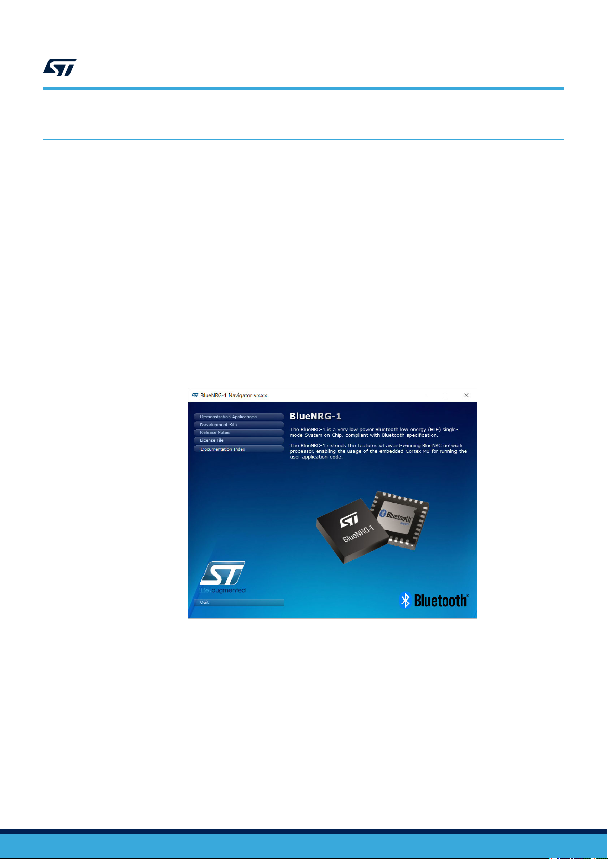
4 BlueNRG-1, BlueNRG-2 Navigator
BlueNRG-1, BlueNRG-2 Navigator are user friendly GUI which lets you select and run demonstration applications
easily
, without requiring any extra hardware. With it, you can access the following DK software package
components:
BlueNRG-1, BlueNRG-2 Bluetooth low energy (BLE) demonstration applications
•
•
BlueNRG-1, BlueNRG-2 peripheral driver examples
• BlueNRG-1, BlueNRG-2 2.4 GHz radio proprietary examples
• BlueNRG-1, BlueNRG-2 development kits
• release notes
• license files
With BlueNRG-1, BlueNRG-2 DK Navigator, you can directly download and run the selected prebuilt application
binary image (BLE examples or peripheral driver example) on the BlueNRG-1, BlueNRG-2 platform without a
JTAG interface.
The interface gives demo descriptions and access to board configurations and source code if needed.
User can run the utility through the BlueNRG-1 and BlueNRG-2 Navigator icon under:
Start → ST BlueNRG -1_2 DK X.X.X → BlueNRG-1 Navigator, BlueNRG-2 Navigator.
UM2071
BlueNRG-1, BlueNRG-2 Navigator
Figure 10. BlueNRG-1 Navigator
Note: BlueNRG-1 Navigator and BlueNRG-2 Navigator are two instances of the same application tailored for the
specific selected device, in order to select the related available resources. Next sections focus on BlueNRG-1
Navigator, but same concepts are also valid for BlueNRG-2 Navigator.
4.1 BlueNRG-1 Navigator ‘Demonstration Applications’
ou can navigate the menus for the reference/demo application you want to launch. For each application, the
Y
following information is provided:
• Application settings (if applicable)
• Application description
• Application hardware related information (e.g., LED signals, jumper configurations, etc.)
The following functions are also available for each application:
UM2071 - Rev 12
page 13/94
UM2071
BlueNRG-1 Navigator ‘Demonstration Applications’
• Flash: to automatically download and run the available prebuilt binary file to a BlueNRG-1 platform
connected to a PC USB port.
• Doc: to display application documentation (html format)
• Project: to open the project folder with application headers, source and project files.
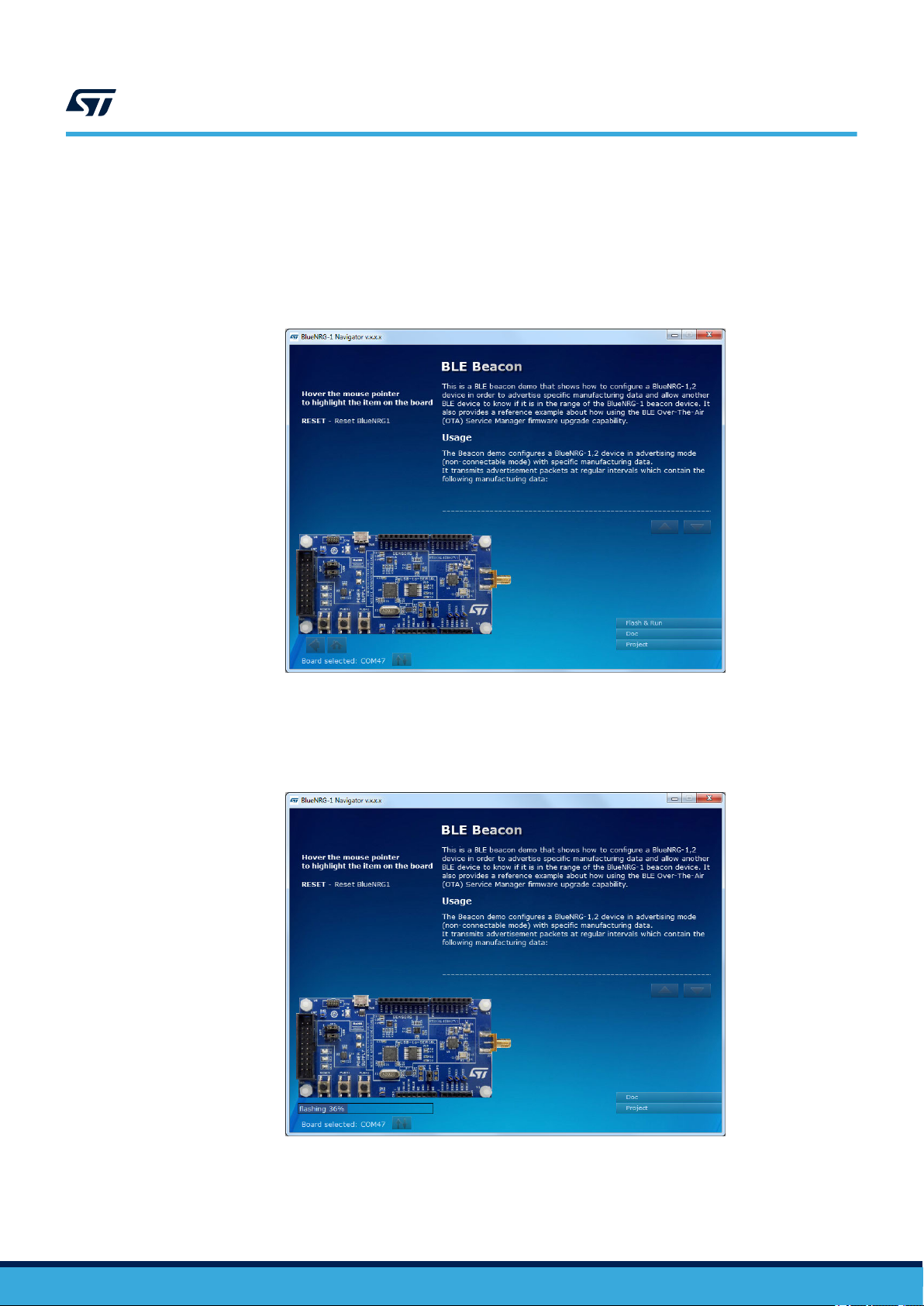
The figure below shows you how to run the BLE Beacon demo application; the other demos function similarly
.
Figure 1
1. BLE Beacon application
When a BlueNRG-1 platform is connected to your PC USB port, you can press the “Flash & Run” tab on the
selected application window to download and run the available prebuilt application binary image on the
BlueNRG-1 platform.
Figure 12. BLE Beacon Flash programming
Selecting the “Doc” tab opens the relative html documentation.
UM2071 - Rev 12
page 14/94
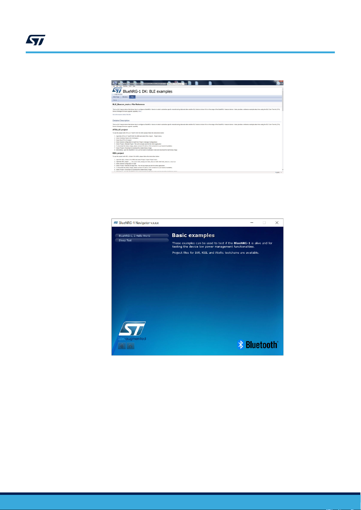
Figure 13. BLE Beacon documentation
4.1.1 BlueNRG-1 Navigator ‘Basic examples’
This page lists some basic sample applications for the BlueNRG-1 device to verify that BlueNRG-1 device is alive
as well as the device sleep and wakeup modes.
Figure 14. Basic examples
UM2071
BlueNRG-1 Navigator ‘Demonstration Applications’
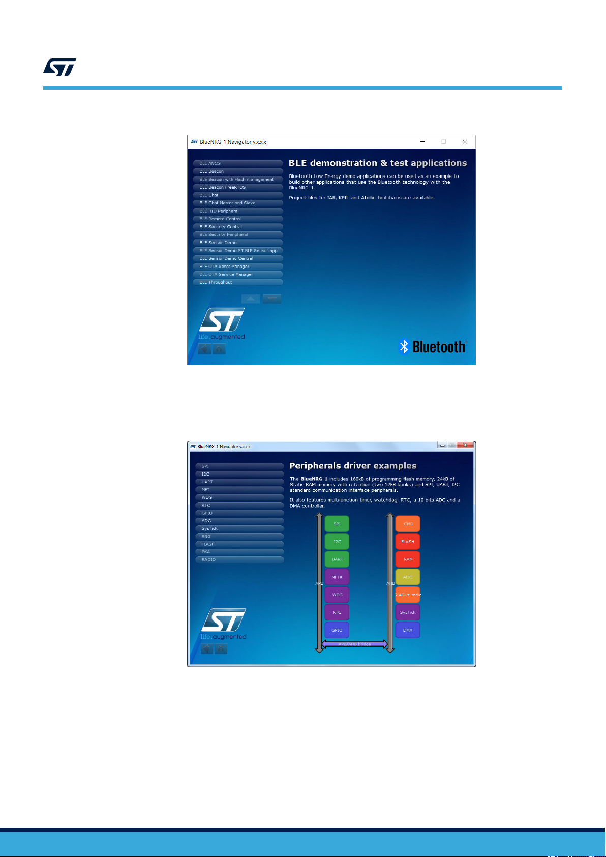
4.1.2 BlueNRG-1 Navigator ‘BLE demonstration and test applications’
This page lists all the available Bluetooth low energy (BLE) demonstration applications in the DK software
package. These applications provide usage examples of the BLE stack features for the BlueNRG-1 device.
UM2071 - Rev 12
page 15/94
BlueNRG-1 Navigator ‘Demonstration Applications’
Figure 15. BLE demonstration and test applications
UM2071
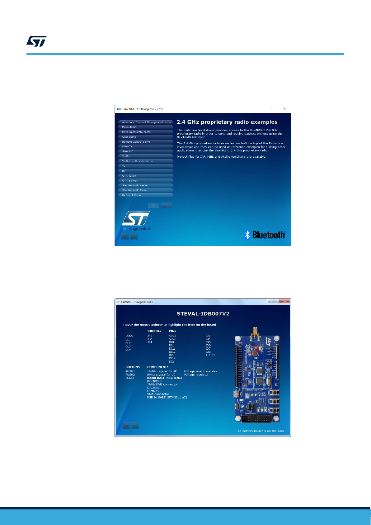
4.1.3 BlueNRG-1 Navigator ‘Peripherals driver examples’
This page lists the available BlueNRG-1 peripherals and corresponding test applications to work with certain
features specific to the selected BlueNRG-1 peripheral.
Figure 16. Peripherals driver examples
4.1.4 BlueNRG-1 Navigator ‘2.4 GHz radio proprietary examples’
The Radio low level driver provides access to the BlueNRG-1 device radio to send and receive packets without
using the Bluetooth link layer
UM2071 - Rev 12
.
page 16/94
UM2071
BlueNRG-1 Navigator ‘Development Kits’
The 2.4 GHz radio proprietary examples built on top of the Radio low level driver can be used as reference
examples for building other applications which use the BlueNRG-1 Radio.
Figure 17. 2.4 GHz radio proprietary examples
4.2 BlueNRG-1 Navigator ‘Development Kits’
This window displays the available BlueNRG-1 DK kit platforms and corresponding resources. When you hover
the mouse pointer on a specific item, the related component is highlighted on the board.
Figure 18. STEVAL-IDB007V2 kit components
4.2.1 BlueNRG-1 Navigator ‘Release Notes’ and ‘License’
As their name suggests, these pages display the DK SW package Release Notes (html format) and the DK
software package license file, respectively.
UM2071 - Rev 12
page 17/94
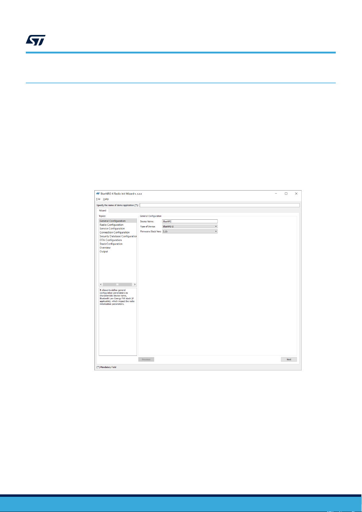
5 BlueNRG-X Radio Init Parameters Wizard
The BlueNRG-X Radio Parameters Wizard is a PC application which allows to define the proper values required
for the correct BlueNRG-1, BlueNRG-2 BLE radio initialization, based on the specific user application scenario. As
consequence of the user choices, a configuration header file (*_config.h) is generated: this file must be used on
the user demonstration application folder
Note:
The BlueNRG-X Radio Init Parameters W
BLUENRG1-DK) supporting BLE stack v2.x family.
5.1 How to run
User can run this utility by clicking on the BlueNRG-X Radio Init Parameters Wizard icon under: Start → ST
BlueNRG -1_2 DK X.X.X
Figure 19. BlueNRG-X Radio Init Parameters Wizard
.
izard is provided only on BlueNRG-1_2 DK SW package (STSW-
UM2071
BlueNRG-X Radio Init Parameters Wizard
5.2 Main user interface window
In the left section of the BlueNRG-X Radio Init Parameters Wizard Utility, user can select the following topics
allowing to define the specific radio initialization parameters based on the specific BLE application requirements:
General Configuration
1.
2. Radio Configuration
3.
Service Configuration
4. Connection Configuration
5. Security DataBase configuration
6. OTA configuration
7. Stack configuration
8. Overview
UM2071 - Rev 12
page 18/94

UM2071
Main user interface window
9. Output
Refer to the BlueNRG-X Radio Init Parameters Wizard documentation available within BlueNRG-1_2 DK SW
package for more details about each provided configuration section.
UM2071 - Rev 12
page 19/94

Programming with BlueNRG-1, BlueNRG-2 system on chip
6 Programming with BlueNRG-1, BlueNRG-2 system on chip
UM2071
The BlueNRG-1, BlueNRG-2 Bluetooth low energy (BLE) stack is provided as a binary library
control BLE functionality
user is simply requested to link this binary library to his or her application and use the relevant APIs to access
BLE functions and complete the stack event callbacks to manage responses according to application
requirements.
A set of software driver APIs is also included for accessing the BlueNRG-1, BlueNRG-2 SoC peripherals and
resources (ADC, GPIO, I²C, MFTX, Micro, R
The development kit software includes sample code demonstrating how to configure BlueNRG-1, BlueNRG-2 and
use the device peripherals and BLE APIs and event callbacks. Documentation on the BLE APIs, callbacks, and
peripheral drivers are provided in separate documents.
. Some callbacks are also provided for user applications to handle BLE stack events. The
TC, SPI, SysTick, UART and WDG).
. A set of APIs to
6.1 Software directory structure
The BlueNRG-1, BlueNRG-2 DK software packages files are organized in the following main directories:
• Application: containing BlueNRG-1, BlueNRG-2 Navigator and Radio Init Parameters Wizard PC
applications.
• Doc: with doxygen BLE APIs and events, BlueNRG-1, BlueNRG-2 peripheral drivers, BLE demo
applications, BlueNRG-1, BlueNRG-2 Peripheral examples, BlueNRG-1, BlueNRG-2 SDK and HAL driver
documentation, DK release notes and license file.
• Firmware: with prebuilt binary BLE and peripheral driver sample applications.
• Library
– Bluetooth LE: Bluetooth low energy stack binary library and all the definitions of stack APIs, stack and
events callbacks. BLE stack v2.1 or later configuration header and source files.
– cryptolib: AES library
– BLE_Application: BLE application framework files (BLE stack layers define values, OTA FW upgrade,
BLE utilities, master library).
– BlueNRG1_Periph_Driver: BlueNRG-1, BlueNRG-2 drivers for device peripherals (ADC, clock, DMA,
Flash, GPIO, I²C, timers, R
– CMSIS: BlueNRG-1 CMSIS files.
– SDK_Eval_BlueNRG1: SDK drivers providing an API interface to the BlueNRG-1, BlueNRG-2 platform
hardware resources (LEDs, buttons, sensors, I/O channel).
– HAL: Hardware abstraction level APIs for abstracting certain BlueNRG-1 hardware features (sleep
modes, clock based on SysTick, etc.).
– STM32L: BlueNRG-1, 2 network coprocessor framework example for an external microcontroller
• Project
– BLE_Examples: Bluetooth low energy demonstration application including Headers, source files and
EWARM, Keil and Atollic project files.
– BlueNRG1_Periph_Examples: with sample applications for the BlueNRG-1, BlueNRG-2 peripherals
and hardware resources, including Headers, source files and project files.
– STM32L: BlueNRG-1, 2 network coprocessor demonstration application examples for an external
microcontroller.
• Utility: contains some utilities
Note: The selection between BlueNRG-1, BlueNRG-2 device is done at compile time using a specific define value
BLUENRG2_DEVICE for selecting BlueNRG-2 device. Default configuration (no define value) selects
BlueNRG-1 device.
Note: BLE_Application folder is available only on BlueNRG-1_2 DK SW package v3.0.0 or later.
Note: Starting from BlueNRG-1_2 DK SW package 3.1.0, Library, Project and Utility folders are located under C:\Users
\{username}\ST\BlueNRG-1_2 DK x.x.x, in order to be able to directly compile projects even with Windows User
Account Control activated.
.
TC, SPI, UARR and watchdog).
UM2071 - Rev 12
page 20/94
7 BLE beacon demonstration application
UM2071
BLE beacon demonstration application
The BLE beacon demo is supported by the BlueNRG-1, BlueNRG-2 development platforms (STEV
AL-IDB008Vx, STEV
STEV
AL-IDB009Vx). It demonstrates how to configure a BlueNRG-1 device to advertise
specific manufacturing data and allow another BLE device to determine whether it is in BLE beacon device range.
7.1 BLE Beacon application setup
This section describes how to configure a BLE device to act as a beacon device.
7.1.1 Initialization
The BLE stack must be correctly initialized thus:
aci_gatt_init();
aci_gap_init(GAP_PERIPHERAL_ROLE, 0, 0x08, &service_handle, &dev_name_char_handle, &appearanc
e_char_handle);
See the BLE stack documentation for more information on these and following commands.
7.1.2 Define advertising data
The BLE Beacon application advertises the following manufacturing data:
Table 5. BlueNRG-1 Beacon advertising manufacturing data
Data field Description Notes
Company identifier code
ID Beacon ID Fixed value
Location UUID Beacons UUID Used to distinguish specific beacons from others
Major number Identifier for a group of beacons Used to group a related set of beacons
Minor number Identifier for a single beacon Used to identify a single beacon
Tx Power 2's complement of the Tx power Used to establish how far you are from device
1. available at: https://www.bluetooth.org/en-us/specification/assigned-numbers/company-identifiers
7.1.3 Entering non-connectable mode
The BLE Beacon device uses the GAP API command to enter non-connectable mode thus:
SIG company identifier
AL-IDB007Vx,
(1)
Default is 0x0030 (STMicroelectronics)
UM2071 - Rev 12
aci_gap_set_discoverable(ADV_NONCONN_IND, 160, 160, PUBLIC_ADDR,
NO_WHITE_LIST_USE,0, NULL, 0, NULL, 0, 0);
To advertise the specific selected manufacturer data, the BLE Beacon application can use the following GAP
APIs:
page 21/94

UM2071
BLE Beacon FreeRTOS example
/* Remove TX power level field from the advertising data: it is necessary to have
enough space for the beacon manufacturing data */
aci_gap_delete_ad_type(AD_TYPE_TX_POWER_LEVEL);
/* Define the beacon manufacturing payload */
uint8_t manuf_data[] = {26, AD_TYPE_MANUFACTURER_SPECIFIC_DATA, 0x30, 0x00,
//Company identifier code (Default is 0x0030 - STMicroelectronics) 0x02,// ID
0x15,//Length of the remaining payload
0xE2, 0x0A, 0x39, 0xF4, 0x73, 0xF5, 0x4B, 0xC4, //Location UUID
0xA1, 0x2F, 0x17, 0xD1, 0xAD, 0x07, 0xA9, 0x61,
0x00, 0x02, // Major number
0x00, 0x02, // Minor number
0xC8//2's complement of the Tx power (-56dB)};
};
/* Set the beacon manufacturing data on the advertising packet */ aci_gap_update_adv_data(27,
manuf_data);
Note: BLE Beacon with Flash Management demonstration application is also available. It allows to configure a Beacon
device as with the original Beacon demo application; it also shows how to properly handle Flash operations
(Erase and Write) and preserve the BLE radio activities. This is achieved by synchronizing Flash operations with
the scheduled BLE radio activities through the aci_hal_end_of_radio_activity_event() event callback timing
information.
7.2 BLE Beacon FreeRTOS example
A specific new Beacon project (BLE_Beacon_FreeRTOS) shows how to use FreeR
TOS with ST BLE stack v2.x.
The example configures a BLE device in advertising mode (non-connectable mode) with specific manufacturing
data and the BTLE_StackTick() is called from a FreeRTOS task (BLETask).
A task randomly changes the Minor number in the advertising data every 500 ms, sending a message through
UART each time. Another task sends other messages through UART every 200 ms and generates a short pulse
on LED3 (visible with a logic analyzer or oscilloscope).
In this example, low priority has been assigned to the BLETask.
Assigning high priority to a BLETask can give better latency; if some tasks require a lot of CPU time, it is
recommended to assign them a lower priority than the BLETask to avoid BLE operations slowing down. Only for
tasks that perform very short sporadic operations before waiting for an event, it is still reasonable to choose a
priority higher than the BLETask.
UM2071 - Rev 12
page 22/94
8 BLE chat demo application
The BLE chat demo (server and client roles) is supported on the BlueNRG-1, BlueNRG-2 development platforms
(STEV
AL-IDB007Vx, STEV
between two BLE devices, demonstrating point-to-point wireless communication using the BlueNRG-1 product.
This demo application exposes a single chat service with the following (20 byte max.) characteristic values:
• The TX characteristic, with which the client can enable notifications; when the server has data to be sent, it
sends notifications with the value of the TX characteristic.
• The RX characteristic, is a writable characteristic; when the client has data to be sent to the server, it writes
a value in this characteristic.
There are two device roles which can be selected through the specific project workspace:
• The Server that exposes the chat service (BLE peripheral device).
• The Client that uses the chat service (BLE central device).
The application requires two devices to be programmed with respective server and client roles. These must be
connected to a PC via USB with an open serial terminal for each device, with the following configurations:
AL-IDB008Vx, STEV
Table 6. Serial port configuration
UM2071
BLE chat demo application
AL-IDB009Vx). It implements simple two-way communication
Parameter Value
Baudrate 115200 bit/s
Data bits 8
Parity bits None
Stop bits 1
The application listens for keys typed in one device terminal and sends them to the remote device when the return
key is pressed; the remote device then outputs the received RF messages to the serial port. Therefore, anything
typed in one terminal becomes visible in the other.
8.1 Peripheral and central device setup
This section describes how two BLE chat devices (server-peripheral and client-central) interact with each other to
set up a point-to-point wireless chat.
BLE device must first be set up on both devices by sending a series of API commands to the processor.
8.1.1 Initialization
The BLE stack must be correctly initialized before establishing a connection with another BLE device. This is
done with aci_gatt_init() and aci_gap_init()
aci_gatt_init();
BLE Chat server role:
APIs:
UM2071 - Rev 12
aci_gap_init(GAP_PERIPHERAL_ROLE, 0, 0x08, &service_handle, &dev_name_char_handle, &appearanc
e_char_handle);
BLE Chat client role:
aci_gap_init(GAP_CENTRAL_ROLE, 0, 0x08, &service_handle, &dev_name_char_handle, &appearance_c
har_handle);
Peripheral and central BLE roles must be specified in the aci_gap_init() command. See the BLE stack API
documentation for more information on these and following commands.
page 23/94

8.1.2 Add service and characteristics
The chat service is added to the BLE chat server device via:
aci_gatt_add_service(UUID_TYPE_128, &service_uuid, PRIMARY_SERVICE, 7,&chatServHandle);
Where service_uuid is the private service 128-bit UUID allocated for the chat service (Primary service). The
command returns the service handle in chatServHandle. The TX characteristic is added using the following
command on the BLE Chat server device:
aci_gatt_add_char(chatServHandle, UUID_TYPE_128, &charUuidTX, 20, CHAR_PROP_NOTIFY, ATTR_PERM
ISSION_NONE, 0, 16, 1, &TXCharHandle);
Where charUuidTX is the private characteristic 128-bit UUID allocated for the TX characteristic (notify property).
The characteristic handle is returned on the TXCharHandle variable.
The RX characteristic is added using the following command on the BLE Chat server device:
aci_gatt_add_char(chatServHandle, UUID_TYPE_128, &charUuidRX, 20, CHAR_PROP_WRITE|CHAR_PROP_W
RITE_WITHOUT_RESP, ATTR_PERMISSION_NONE, GATT_SERVER_ATTR_WRITE,16, 1, &RXCharHandle);
Where charUuidRX is the private characteristic 128-bit UUID allocated for the RX characteristic (write property).
The characteristic handle is returned on the RXCharHandle
See the BLE stack API documentation for more information on these and following commands.
UM2071
Peripheral and central device setup
variable.
8.1.3 Enter connectable mode
The server device uses GAP API commands to enter the general discoverable mode:
aci_gap_set_discoverable(ADV_IND, 0, 0, PUBLIC_ADDR, NO_WHITE_LIST_USE,8,local_name, 0, NULL,
0, 0);
The local_name parameter contains the name presented in advertising data, as per Bluetooth core specification
version 4.2, V
ol. 3, Part C, Ch. 11.
8.1.4 Connection with central device
Once the server device is discoverable by the BLE chat client device, the client device uses
aci_gap_create_connection()to connect with the BLE chat server device:
aci_gap_create_connection(0x4000, 0x4000, PUBLIC_ADDR, bdaddr, PUBLIC_ADDR, 40, 40, 0, 60, 20
00 , 2000);
Where bdaddr is the peer address of the client device.
Once the two devices are connected, you can set up corresponding serial terminals and type messages in either
of them. The typed characters are stored in two respective buffers and when the return key is pressed:
• on the BLE chat server device, the typed characters are sent to the BLE chat client device by notifying the
previously added TX characteristic (after notifications are enabled) with:
aci_gatt_update_char_value(chatServHandle,TXCharHandle,0,len, (uint8_t*)cmd+j);
• on the BLE chat client device, the typed characters are sent to the BLE chat server device by writing the
previously added RX characteristic with:
UM2071 - Rev 12
aci_gatt_write_without_resp(connection_handle, rx_handle+1, len, (uint8_t *)cmd+j);
Where connection_handle is the handle returned upon connection as a parameter of the connection complete
event, rx_handle is the RX characteristic handle discovered by the client device.
Once these API commands have been sent, the values of the TX and RX characteristics are displayed on the
serial terminals.
page 24/94
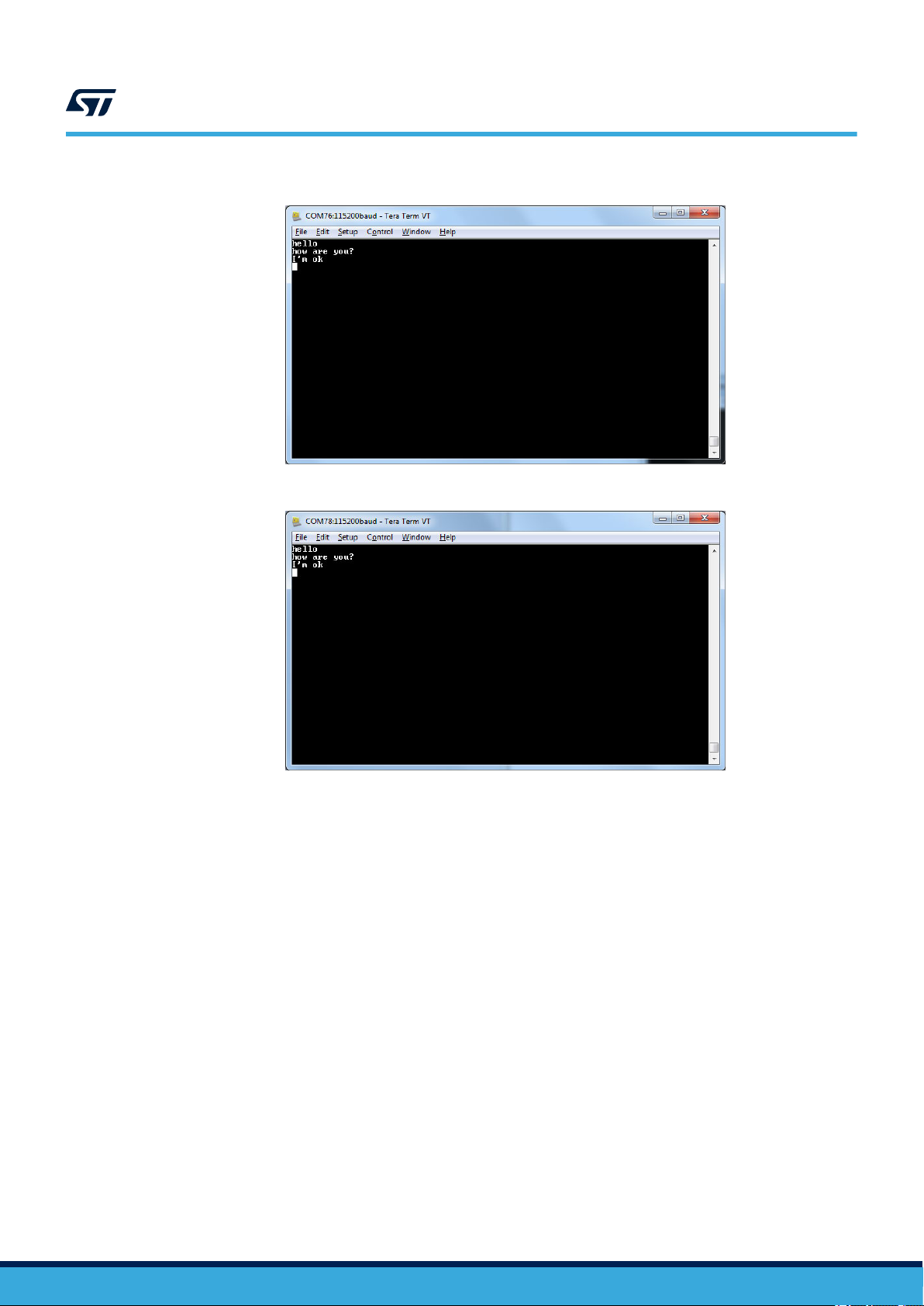
Figure 20. BLE chat client
Figure 21. BLE chat server
UM2071
Peripheral and central device setup
UM2071 - Rev 12
page 25/94

BLE chat master and slave demo application
9 BLE chat master and slave demo application
The BLE chat master and slave demo is supported on the BlueNRG-1, BlueNRG-2development platforms
(STEV
AL-IDB007Vx, STEV
communication using a single application which configures the chat client and server roles at runtime.
The new chat demo application configures a BLE device as central or peripheral using the API:
aci_gap_init(GAP_CENTRAL_ROLE|GAP_PERIPHERAL_ROLE, 0, 0x07, &service_handle, &dev_name_char_h
andle, &appearance_char_handle);
It then initiates a discovery procedure for another BLE device configured with the same chat master and slave
application image.
If such a device is found within a random interval, it starts a connection procedure and waits until a connection is
established. If the discovery procedure time expires without finding another chat master and slave device, the
device enters discovery mode and waits for another chat master and slave device to discover and connect to it.
When connection is established, the client and server roles are defined and the chat communication channel can
be used.
This demo application exposes a single chat service with the following (20 byte max.) characteristic values:
•
The TX characteristic, with which the client can enable notifications; when the server has data to be sent, it
sends notifications with the value of the TX characteristic.
• The RX characteristic, is a writable characteristic; when the client has data to be sent to the server, it writes
a value in this characteristic.
The application requires two devices to be programmed with the same application, with the server and client roles
defined at runtime. Connect the two devices to a PC via USB and open a serial terminal on both with the same
configuration as T
The application listens for keys typed in one device terminal and sends them to the remote device when the return
key is pressed; the remote device then outputs the received RF messages to the serial port. Therefore, anything
typed in one terminal becomes visible in the other.
able 6. Serial port configuration.
AL-IDB008Vx, STEV
AL-IDB009Vx). It demonstrates simple point-to-point wireless
UM2071
9.1 BLE chat master and slave roles
This section describes how two BLE chat master and slave devices interact with each other in order to set up a
point-to-point wireless chat.
The BLE stack must first be set up on both devices by sending a series of API commands to the processor
chat master and slave client and server roles are defined at runtime.
9.1.1 Initialization
The BLE stack must be correctly initialized before establishing a connection with another BLE device. This is
done with two commands:
aci_gatt_init();
aci_gap_init(GAP_CENTRAL_ROLE|GAP_PERIPHERAL_ROLE, TRUE,0x07, &service_handle, &dev_name_char
_handle, &appearance_char_handle);
The BLE peripheral and central roles are specified in the aci_gap_init() command. See the BLE API
documentation for more information on these and following commands.
9.1.2 Add service and characteristics
Refer to Section 8.1.2 Add service and characteristics.
9.1.3 Start discovery procedure
To find another BLE chat master and slave device in discovery mode, a discovery procedure must be started via:
aci_gap_start_general_discovery_proc(0x4000, 0x4000, 0x00, 0x00);
. The
UM2071 - Rev 12
page 26/94

9.1.4 Enter connectable mode
The following GAP API command is used for entering general discoverable mode:
aci_gap_set_discoverable(ADV_IND, 0x90, 0x90, PUBLIC_ADDR, NO_WHITE_LIST_USE, sizeof(local_na
me), local_name, 0, NULL, 0x6, 0x8);
9.1.5 Connection with chat master and slave client device
In the above mentioned discovery and mode assignment procedures, the two chat master and slave applications
assume respective client and server roles at runtime. During this initial configuration phase, when a chat master
and slave device is placed in discoverable mode and it is found by the other chat master and slave device
performing a discovery procedure, a Bluetooth low energy connection is created and the device roles are defined.
The following GAP API command is used for connecting to the discovered device:
aci_gap_create_connection(0x4000, 0x4000,device_found_address_type, device_found_address, PUB
LIC_ADDR, 40, 40, 0, 60, 2000 , 2000);
Where device_found_address_type is the address type of the discovered chat master and slave and
device_found_address is the peer address of the discovered chat master and slave device.
Once the two devices are connected, you can set up corresponding serial terminals and type messages in either
of them. The typed characters are stored in two respective buf
On the BLE chat master-and-slave server device, the typed characters are sent to the master-and-slave client
device by notifying the previously added TX characteristic (after notifications have been enabled). This is done
via:
UM2071
BLE chat master and slave roles
fers and when the return key is pressed:
aci_gatt_update_char_value(chatServHandle, TXCharHandle, 0, len, (uint8_t *)cmd+j);
On the master-and-slave client device, the typed characters are sent to the master-and-slave server device, by
writing the previously added RX characteristic. This is done via:
aci_gatt_write_without_resp (connection_handle, rx_handle +1, len, (uint8_t *)cmd+j);
Where connection_handle is the handle returned upon connection as a parameter of the connection complete
event, rx_handle is the RX characteristic handle discovered by the client device.
Once these API commands have been sent, the values of the TX and RX characteristics are displayed on the
serial terminals.
UM2071 - Rev 12
page 27/94

10 BLE remote control demo application
UM2071
BLE remote control demo application
The BLE remote control application is supported on the BlueNRG-1, BlueNRG-2
AL-IDB007Vx, STEV
(STEV
(like an actuator) using a BlueNRG-1, BlueNRG-2 device.
This application periodically broadcasts temperature values that can be read by any device. The data is
encapsulated in a manufacturer-specific AD type and the content (besides the manufacturer ID, i.e., 0x0030 for
STMicroelectronics) is as follows:
Byte 0 Byte 1 Byte2
App ID (0x05) Temperature value (little-endian)
The temperature value is given in tenths of degrees Celsius.
The device is also connectable and exposes a characteristic used to control LEDs DL1 and DL3 on the BLE kit
platform. The value of this characteristic is a bitmap of 1 byte. Each bit controls one of the LEDs:
•
bit 0 is the status of LED DL1
• bit 2 is the status of LED DL3.
A remote device can therefore connect and write this byte to change or read the status of these LEDs (1 for LED
ON, 0 for LED OFF).
The peripheral disconnects after a timeout (DISCONNECT_TIMEOUT) to prevent a central device remaining
connected to the device indefinitely.
Security is not enabled by default, but this can be changed with ENABLE_SECURITY (refer to file
BLE_RC_main.h). When security is enabled, the central device must be authenticated before reading or writing
the device characteristic.
To interact with a device configured as a BLE remote control, another BLE device (a BlueNRG-1, BlueNRG-2 or
any Bluetooth® Low Energy device) can be used to detect and view broadcast data.
To control one of the LEDs, the device has to connect to a BlueNRG-1 BLE remote control device and write in the
exposed control point characteristic. The Service UUID is ed0ef62e-9b0d-11e4-89d3-123b93f75cba. The control
point characteristic UUID is ed0efb1a-9b0d-11e4-89d3-123b93f75cba.
AL-IDB008Vx, STEVAL-IDB009Vx). It demonstrates how to control a remote device
Table 7. BLE remote advertising data
development platforms
10.1 BLE remote control application setup
This section describes how to configure a BlueNRG-1
10.1.1 Initialization
The BLE stack must be correctly initialized before establishing a connection with another Bluetooth LE device.
This is done with two commands:
aci_gatt_init();
aci_gap_init(GAP_PERIPHERAL_ROLE, 0, 0x07, &service_handle, &dev_name_char_handle, &appearanc
e_char_handle);
See BLE stack API documentation for more information on these and following commands.
10.1.2 Define advertising data
The BLE remote control application advertises certain manufacturing data as follows:
UM2071 - Rev 12
device to acting as a remote control device.
page 28/94

/* Set advertising device name as Node */
const uint8_t scan_resp_data[] = {0x05,AD_TYPE_COMPLETE_LOCAL_NAME,'N','o','d','e'}
/* Set scan response data */ hci_le_set_scan_response_data(sizeof(scan_resp_data),scan_resp
_data);
/* Set Undirected Connectable Mode */
aci_gap_set_discoverable(ADV_IND, (ADV_INTERVAL_MIN_MS*1000)/625,
(ADV_INTERVAL_MAX_MS*1000)/625, PUBLIC_ADDR, NO_WHITE_LIST_USE, 0, NULL, 0, NULL, 0, 0);
/* Set advertising data */
hci_le_set_advertising_data(sizeof(adv_data),adv_data);
On the development platform, the temperature sensor value is set in the adv_data variable.
10.1.3 Add service and characteristics
The BLE Remote Control service is added via:
aci_gatt_add_service(UUID_TYPE_128, &service_uuid, PRIMARY_SERVICE, 7,
&RCServHandle);
Where service_uuid is the private service 128-bit UUID allocated for the BLE remote service
(ed0ef62e-9b0d-1
The command returns the service handle in RCServHandle.
The BLE remote control characteristic is added using the following command:
1e4-89d3-123b93f75cba).
UM2071
BLE remote control application setup
#if ENABLE_SECURITY
aci_gatt_add_char(RCServHandle, UUID_TYPE_128, &controlPointUuid, 1,
CHAR_PROP_READ|CHAR_PROP_WRITE|CHAR_PROP_WRITE_WITHOUT_RESP|CH AR_PROP_SIGNED_WRITE,
ATTR_PERMISSION_AUTHEN_READ|ATTR_PERMISSION_AUTHEN_WRITE, GATT_NOTIFY_ATTRIBUTE_WRITE,16,1,&c
ontrolPointHandle);
#else
aci_gatt_add_char(RCServHandle, UUID_TYPE_128, &controlPointUuid, 1,
CHAR_PROP_READ|CHAR_PROP_WRITE|CHAR_PROP_WRITE_WITHOUT_RESP, ATTR_PERMISSION_NONE, GATT_NOTIF
Y_ATTRIBUTE_WRITE, 16,
1,&controlPointHandle);
#endif
Where controlPointUuid is the private characteristic 128-bit UUID allocated for BLE remote control
characteristic (ed0efb1a-9b0d-1
1e4-89d3-123b93f75cba) and controlPointHandle is the BLE remote control
characteristic handle.
If security is enabled, the characteristic properties must be set accordingly to enable authentication on
controlPointUuid characteristic read and write.
10.1.4 Connection with a BLE Central device
When connected to a BLE central device (another BlueNRG-1,
device), the controlPointUuid characteristic is used to control the BLE remote control platform LED. Each
time a write operation is performed on controlPointUuid, the aci_gatt_attribute_modified_event()
callback is raised and the selected LEDs are turned on or of
BlueNRG-2 device or any Bluetooth® Low Energy
f.
UM2071 - Rev 12
page 29/94

11 BLE sensor profile demo
UM2071
BLE sensor profile demo
The BLE sensor profile demo is supported on the BlueNRG-1, BlueNRG-2 development platforms (STEV
IDB007Vx, STEV
sensor profile.
This example is useful for building new profiles and applications that use the BlueNRG-1, BlueNRG-2 SoC. The
GATT profile is not compliant with any existing specifications as the purpose of this project is to simply
demonstrate how to implement a given profile.
This profile exposes the acceleration and environmental services.
Figure 22. BLE sensor demo GATT database shows the whole GATT database, including the GATT (0x1801) and
GAP (0x1800) services that are automatically added by the stack.
The acceleration service free fall characteristic cannot be read or written, but can be signaled. The application
sends notification of this characteristic (with a value of 0x01) if a free fall condition is detected by the MEMS
sensor (when the acceleration on the three axes is near zero for a certain amount of time). Notifications can be
enabled or disabled by writing the associated client characteristic configuration descriptor.
The other characteristic exposed by the service gives the current value of the acceleration measured by the
accelerometer in six bytes. Each byte pair contains the acceleration on one of the three axes. The values are
given in mg. This characteristic is readable and can be notified if notifications are enabled.
Another service is defined, which contains characteristics that expose data from some environmental sensors:
temperature and pressure. Each characteristic data type is described in a format descriptor. All of the
characteristics have read-only properties.
AL-IDB008Vx, STEV
AL-IDB009Vx). It implements a proprietary, Bluetooth low energy (BLE)
Figure 22. BLE sensor demo GATT database
AL-
11.1 BlueNRG app for smartphones
An application is available for iOS™ and Android™ smartphones or tablets that also works with the BLE sensor
profile demo. This app enables notification of the acceleration characteristic and displays the value on screen.
Data from environmental sensors are also periodically read and displayed.
UM2071 - Rev 12
page 30/94

BLE sensor profile demo: connection with a central device
Figure 23. BlueNRG sensor app
UM2071
11.2 BLE sensor profile demo: connection with a central device
This section describes how to interact with a central device, while the BLE stack is acting as a peripheral. The
central device may be another BlueNRG-1, BlueNRG-2 device acting as a BLE master, or any other Bluetooth
Low Energy device.
The BLE stack must first be set up by sending a series of BLE API commands to the processor.
11.2.1 Initialization
The BLE stack must be correctly initialized before establishing a connection with another Bluetooth LE device.
This is done via:
aci_gatt_init();
aci_gap_init(GAP_PERIPHERAL_ROLE, 0, 0x07, &service_handle, &dev_name_char_handle, &appearanc
e_char_handle);
See BLE stack API documentation for more information on these and following commands.
11.2.2 Add service and characteristics
The BlueNRG-1 BLE stack has both server and client capabilities. A characteristic is an element in the server
database where data is exposed, while a service contains one or more characteristics. The acceleration service is
added with the following command:
aci_gatt_add_service(UUID_TYPE_128, &service_uuid, PRIMARY_SERVICE, 7,
&accServHandle);
The command returns the service handle on variable accServHandle. The free fall and acceleration
characteristics must now be added to this service thus:
UM2071 - Rev 12
aci_gatt_add_char(accServHandle, UUID_TYPE_128, &char_uuid, 1, CHAR_PROP_NOTIFY,
ATTR_PERMISSION_NONE, 16, 0, &freeFallCharHandle);
aci_gatt_add_char(accServHandle, UUID_TYPE_128, &char_uuid, 6, CHAR_PROP_NOTIFY|CHAR_PROP_REA
D,
ATTR_PERMISSION_NONE, GATT_NOTIFY_READ_REQ_AND_WAIT_FOR_APPL_RESP, 16, 0, &accCharHandle);
The free fall and acceleration characteristics handles are returned on freeFallCharHandle and
accCharHandle variables respectively
.
page 31/94

Similar steps are followed for adding the environmental sensor and relative characteristics.
11.2.3 Enter connectable mode
Use GAP API command to enter one of the discoverable and connectable modes:
aci_gap_set_discoverable(ADV_IND, (ADV_INTERVAL_MIN_MS*1000)/625,
ADV_INTERVAL_MAX_MS*1000)/625, STATIC_RANDOM_ADDR, NO_WHITE_LIST_USE sizeof(local_name), loca
l_name, 0, NULL, 0, 0);
Where
local_name[] = {AD_TYPE_COMPLETE_LOCAL_NAME,'B','l','u','e','N','R','G'};
The local_name parameter contains the name presented in advertising data, as per Bluetooth core specification
version, V
1.2.4 Connection with central device
1
Once the BLE stack is placed in discoverable mode, it can be detected by a central device. The smartphone app
described in Section 11.1 BlueNRG app for smartphones is designed for interact with the sensor profile demos
(it also supports the BlueNRG-1 device).
Any Bluetooth Low Energy device like a smartphone can connect to the BLE sensor profile demo.
For example, the LightBlue application in Apple Store® connects iPhone® versions 4S/5 and above can connect
to the sensor profile device. When you use the LightBlue application, detected devices appear on the screen with
the BlueNRG name. By tapping on the box to connect to the device, a list of all the available services is shown on
the screen; tapping a service shows the characteristics for that service.
The acceleration characteristic can be notified using the following command:
ol. 3, Part C, Ch. 11.
UM2071
BLE sensor profile demo: connection with a central device
aci_gatt_update_char_value(accServHandle, accCharHandle, 0, 6, buff);
Where buff is a variable containing the three axes acceleration values.
Once this API command has been sent, the new value of the characteristic is displayed on the phone.
UM2071 - Rev 12
page 32/94

12 BLE sensor profile central demo
The BLE sensor profile central demo is supported on the BlueNRG-1, BlueNRG-2 development platforms
(STEV
AL-IDB007Vx, STEV
Profile Central role which emulates the Sensor Demo applications available for smartphones (iOS and android).
This application configures a BlueNRG-1, BlueNRG-2 device as a Sensor device, Central role which is able to
find, connect and properly configure the free fall, acceleration and environment sensors characteristics provided
by a BLE development platform configured as a BLE Sensor device, Peripheral role (refer to Section 11 BLE
sensor profile demo).
This application uses a new set of APIs allowing to perform the following operations on a BlueNRG-1, BlueNRG-2
Master/Central device:
• Master Configuration Functions
• Master Device Discovery Functions
• Master Device Connection Functions
• Master Discovery Services, Characteristics Functions
• Master Data Exchange Functions
• Master Security Functions
• Master Common Services Functions
These APIs are provided through a binary library and they are fully documented on available doxygen
documentation within the DK SW package. The following master/central binary libraries are provided in Library
\BLE_Application\Profile_Central\library folder: libmaster_library_bluenrg1.a for IAR, Keil and Atollic toolchains on
STSW-BLUENRG1-DK SW package.
AL-IDB008Vx, STEV
AL-IDB009Vx). It implements a basic version of the BLE Sensor
UM2071
BLE sensor profile central demo
UM2071 - Rev 12
page 33/94

13 BLE HID/HOGP demonstration application
The BLE HID/HOGP demonstration applications are supported by the BlueNRG-1, BlueNRG-2development
platforms (STEV
standard HID/HOGP Bluetooth low energy application profile. Keyboard and mouse demo examples are provided.
AL-IDB007Vx, STEV
13.1 BLE HID/HOGP mouse demonstration application
The BLE HID mouse application implements a basic HID mouse with two buttons compliant with the standard
HID/HOGP BLE application profile.
The HID mouse device is named ‘STMouse’ in the central device list.
The mouse movements are provided by the 3D accelerometer and 3D gyroscope on the BLE development
platform.
•
The left button is the ‘PUSH1’ button.
• The right button is the ‘PUSH2’ button
If the HID mouse is not used for two minutes, it closes the connection and enters deep sleep mode. This idle
connection timeout can be changed from the application. To exit deep sleep mode, press the left PUSH1 button or
reset the platform.
AL-IDB008Vx, STEV
AL-IDB009Vx). It demonstrates a BLE device using the
UM2071
BLE HID/HOGP demonstration application
13.2 BLE HID/HOGP keyboard demonstration application
The BLE HID keyboard application implements a basic HID keyboard compliant with the standard HID/HOGP
BLE application profile.
The HID mouse device is named ‘STKeyboard’ in the central device list.
T
o successfully complete the bonding and pairing procedure, insert the PIN: 123456.
o use the HID keyboard:
T
•
Connect the BLE development platform to a PC USB port
• Open a HyperTerminal window (115200, 8, N,1)
• Put the cursor focus on the HyperTerminal window
• The keys that are sent to the central device using the HID/HOGP BLE application profile are also shown on
the HyperTerminal window
If the HID keyboard is not used for two minutes, it closes the connection and enters deep sleep mode. This idle
connection timeout can be changed from the application. To exit deep sleep mode, press the left PUSH1 button or
reset the platform.
UM2071 - Rev 12
page 34/94

14 BLE throughput demonstration application
The BLE throughput demonstration application provides some basic throughput demonstration applications to
provide some reference figures regarding the achievable Bluetooth low energy data rate using the BlueNRG-1,
BlueNRG-2 device.
The throughput application scenarios provided are:
1.
Unidirectional scenario: the server device sends characteristic notifications to a client device.
Bidirectional scenario: the server device sends characteristic notifications to a client device and client device
2.
sends write without response characteristics to the server device.
The throughput application exposes one service with two (20 byte max.) characteristic values:
•
The TX characteristic, with which the client can enable notifications; when the server has data to be sent, it
sends notifications with the value of the TX characteristic.
• The RX characteristic, is a writable characteristic; when the client has data to be sent to the server, it writes
a value in this characteristic.
The device roles which can be selected are:
1. Server, which exposes the service with the TX, RX characteristics (BLE peripheral device)
2. Client, which uses the service TX, RX characteristics (BLE central device).
Each device role has two instances for each throughput scenario (unidirectional, bidirectional).
The BLE throughput demonstration applications are supported by the BlueNRG-1, BlueNRG-2 development
platforms (STEVAL-IDB007Vx, STEVAL-IDB008Vx, STEVAL-IDB009Vx).
UM2071
BLE throughput demonstration application
14.1 BLE unidirectional throughput scenario
The unidirectional throughput scenario lets you perform a unidirectional throughput test where a server device
sends notification to a client device.
T
o run this scenario:
• Program the client unidirectional application on one BLE platform and reset it. The platform is seen on the
PC as a virtual COM port.
Open the port in a serial terminal emulator (the required serial port baudrate is 921600)
•
• Program the server unidirectional application on a second BLE platform and reset it.
• The two platforms try to establish a connection; if successful, the slave continuously sends notifications of
TX characteristic (20 bytes) to the client.
• After every 500 packets, the measured application unidirectional throughput is displayed.
14.2 BLE bidirectional throughput scenario
The bidirectional throughput scenario lets you perform a bidirectional throughput test where the server device
sends notifications to a client device and client device sends write without response characteristics to the server
device.
T
o run this scenario:
• Program the client bidirectional application on one BLE platform and reset it. The platform is seen on the PC
as a virtual COM port.
•
Open the related port in a serial terminal emulator (the required serial port baudrate is 921600)
• Program the server bidirectional application on a second BLE platform and reset it.
• Open the related port in a serial terminal emulator (the required serial port baudrate is 921600)
• The two platforms try to establish a connection; if successful, the slave device continuously sends
notifications of TX characteristic (20 bytes) to the client device and the client device continuously sends write
without responses of the RX characteristic (20 bytes) to the server device.
• After every 500 packets, the measured application bidirectional throughput is displayed.
UM2071 - Rev 12
page 35/94

UM2071
BLE bidirectional throughput scenario
Note: For BlueNRG-2, BLE stack v2.1 or later
extension up to 251 bytes) is provided. The application allows displaying the throughput data in a unidirectional
flow (the server sends notifications to the client) or a bidirectional flow (the server sends notifications to the client
and the client writes without response operations on the server). The server can perform an ATT_MTU
exchange operation to increase the A
TT_MTU size to 247 bytes. The user can also directly set the actual data
length value up to 247 bytes.
, a further BLE throughput demonstration application (with data length
UM2071 - Rev 12
page 36/94

BLE notification consumer demonstration application
15 BLE notification consumer demonstration application
The BLE ANCS demonstration application configures a BlueNRG-1, BlueNRG-2 device as a BLE notification
consumer
provider
After reset, the demo places the BLE device in advertising with device name "ANCSdemo" and sets the
BlueNRG-1 authentication requirements to enable bonding.
When the device is connected and bonded with a notification provider, the demo configures the BLE notification
consumer device to discover the service and the characteristics of the notification provider. When the setup phase
is complete, the BLE device is configured as a notification consumer able to receive the notifications sent from the
notification provider
The BLE notification consumer demonstration application is supported by the BlueNRG-1, BlueNRG-2
development platforms (STEVAL-IDB007Vx, STEVAL-IDB008Vx, STEVAL-IDB009Vx).
, which facilitates Bluetooth accessory access to the many notifications generated on a notification
.
.
UM2071
UM2071 - Rev 12
page 37/94

16 BLE security demonstration applications
The BLE Security demonstration applications are supported by the BlueNRG-1, BlueNRG-2 development
platforms (STEV
respectively
AL-IDB007Vx, STEV
, two BLE devices as a Central and Peripheral, and setup a secure connection by performing a BLE
pairing procedure. Once paired the two devices are also bonded.
The following pairing key generation methods are showed:
• PassKey entry with random pin
• PassKey entry with fixed pin
• Just works
• Numeric Comparison (new paring method supported only from BlueNRG-1, BlueNRG-2 BLE stack v2.x)
For each pairing key generation method, a specific project security configuration is provided for both Central &
Peripheral device as shown in the following Table 8. BLE security demonstration applications security
configurations combinations. Each Central and Peripheral device must be loaded, respectively, with the
application image targeting the proper security configuration, to correctly demonstrate the associated BLE
security pairing functionality.
AL-IDB008Vx). They provide some basic examples about how to configure,
UM2071
BLE security demonstration applications
Table 8. BLE security demonstration applications security configurations combinations
Pairing key generation method Central device security configuration
PassKey entry with random pin Master_PassKey_Random Slave_PassKey_Random
PassKey entry with fixed pin Master_PassKey_Fixed Slave_PassKey_Fixed
Just works Master_JustWorks Slave_JustWorks
Numeric Comparison Master_NumericComp Slave_NumericComp
16.1 Peripheral device
On reset, after initialization, Peripheral device sets security IO capability and authentication requirements, in order
to address the selected pairing key generation method, in combinations with the related security settings of the
Central device.
After initialization phase, Peripheral device also defines a custom service with 2 proprietary characteristics (UUID
128 bits):
- TX characteristic: notification (CHAR_PROP_NOTIFY),
- RX characteristic with properties: read (CHAR_PROP_READ,
GATT_NOTIFY_READ_REQ_AND_WAIT_FOR_APPL_RES
is received for this attribute).
Based on the selected security configuration, the RX characteristic is defined with proper security permission (link
must be "encrypted to read" on JustWorks method, link must be "encrypted to read and need authentication to
read" on all other methods).
The Peripheral device enters in discovery mode with local name SlaveSec_Ax (x= 0,1,2,3 depending on the
selected security configuration).
Peripheral device security
configuration
(application is notified when a read request of any type
UM2071 - Rev 12
Table 9. Peripheral device advertising local name parameter value
Peripheral device configuration Advertising local name Pairing method
Slave_JustWorks SlaveSec_A0 Just works
Slave_PassKey_Fixed SlaveSec_A1 PassKey entry with fixed pin
Slave_PassKey_Random SlaveSec_A2 PassKey entry with random pin
Slave_NumericComp SlaveSec_A3 Numeric Comparison
page 38/94

UM2071
Central device
When a Central device starts the discovery procedure and detects the Peripheral device, the two devices
connects.
After connection, Peripheral device starts a slave security request to the Central device
aci_gap_slave_security_req() and , as consequence, Central devices starts pairing procedure.
Based on the pairing key generation method, user could be asked to perform some actions (i.e. confirm the
numeric value if the numeric comparison configuration is selected, add the key
on Central hyper terminal, if the passkey entry with random pin configuration is selected).
After devices pairs and get bonded, Peripheral device displays the list of its bonded devices and configures its
white list in order to add the bonded Central device to its white list aci_gap_configure_whitelist() API.
Central devices starts the service discovery procedure to identify the Peripheral service and characteristics and,
then, enabling the TX characteristic notification.
Peripheral device starts TX characteristic notification to the Central device at periodic interval, and it provides the
RX characteristic value to the Central device each time it reads it.
When connected, if user presses the BLE platform button PUSH1, Peripheral device disconnects and enters
undirected connectable mode mode with advertising filter enabled (WHITE_LIST_FOR_ALL: Process scan and
connection requests only from devices in the white list). This implies that Peripheral device accepts connection
requests only from devices on its white list: Central device is still be able to connect to the Peripheral device; any
other device connection requests are not accepted from the Peripheral device.
TX and RX characteristics length is 20 bytes and related values are defined as follow: - TX characteristic value:
{'S','L','A','V','E','_','S','E','C','U','R','I','T','Y','_','T','X',' ',x1,x2};
where x1, x2 are counter values - RX characteristic value:
{'S','L','A','V','E','_','S','E','C','U','R','I','T','Y','_','R','X',' ',x1,x2};
where x1, x2 are counter values
, displayed on Peripheral device,
16.2 Central device
On reset, after initialization, Central device uses the Master_SecuritySet() API for setting the security IO
capability and authentication requirements in order to address the specific selected paring method, in
combinations with the related security settings of the Central device. Central device application is using the
Central/Master library APIs and callbacks for performing the Central device BLE operations (device discovery
connection, …).
Central device starts a device discovery procedure (Master_DeviceDiscovery() API, looking for the
associated Peripheral device SlaveSec_Ax
name parameter value).
When found, Central connects to the Peripheral device. In order to start the pairing, Central device is expecting
the Peripheral device to send a slave security request. Once the security request is received, Central device
starts the pairing procedure. Based on the pairing key generation method, user could be asked to perform some
actions (i.e. confirm the numeric value if the numeric comparison configuration is selected, add the key, displayed
on Peripheral device, on Central hyper terminal, if the passkey entry with random pin configuration is selected).
Once the pairing and bonding procedure has been completed, the Central device starts the service discovery
procedure in order to find the Peripheral TX & RX characteristics.
After Service Discovery, Central enables the TX characteristic notification. Then the Central device receives
periodically the TX characteristic notification value from Peripheral device and read the related RX characteristic
value from Peripheral device.
When connected, if user presses the BLE platform PUSH1 button, the Central device disconnects and reconnect
to the Peripheral device which enters in undirected connectable mode with advertising filter enabled. Once
connected to the Peripheral device, it enters again on the TX characteristic notification/RX characteristic read
cycle.
(x= 0,1,2,3 : refer to
,
Table 9. Peripheral device advertising local
UM2071 - Rev 12
page 39/94

UM2071
Central device
Note: When using a smarthphone as Central device, if this device uses a random resolvable address, the Periheral
device is not able to accept connection or scan requests coming from it, during the reconnection phase.
This is due to the fact that, when disconnecting, the Peripheral device enters the undirected connectable mode
with filtering enabled (WHITE_LIST_FOR_ALL: process scan and connection requests from the White List
devices only). As a consequence, it is able to accept the smarthphone scan or connection requests, only if the
Privacy Controller is enabled on the Peripheral device.
A possible simple alternative is to replace, on the Peripheral device, the WHITE_LIST_FOR_ALL advertising
filter policy with NO_WHITE_LIST_USE: the Peripheral device does not enable device filtering after
reconnection, and it is able to accept connection or scan requests coming from a smartphone by using
resolvable random addresses.
UM2071 - Rev 12
page 40/94

UM2071
BLE power consumption demo application
17 BLE power consumption demo application
The BLE power consumption demo application allows putting the selected BLE device in discovery mode: you
can choose from a test menu which advertising interval to use (100 ms or 1000 ms). T
BlueNRG-2 current consumption, it is necessary to connect a DC power analyzer to the JP4 connector of the
AL-IDB007Vx, STEV
STEV
with another device configured as a master and measure the related power consumption.
The master role can be covered by another BlueNRG-1, BlueNRG-2 kit platform configured with the DTM FW
application (DTM_UART.hex) and running a specific script through the BlueNRG GUI or Script launcher PC
applications.
In the BLE_Power_Consumption demo application project folder, two scripts are provided to configure the master
device and create a connection with the BlueNRG-1, 2 kit platform under test.
The two scripts allow establishing a connection with 100 ms and 1000 ms as connection intervals, respectively.
The power consumption demo supports some test commands:
• f: the device is in discoverable mode with a fast interval of 100 ms
• s: the device is in discoverable mode with a slow interval of 1000 ms
• r: to reset the BlueNRG-1
• ?: to display the help menu
Note: This demo application is available only on BlueNRG-1_2 DK SW package (STSW-BLUENRG1-DK) supporting
BLE stack v2.x family.
AL-IDB008Vx, STEVAL-IDB009Vx kit platforms. Then, you can set a connection up
o measure the BlueNRG-1,
UM2071 - Rev 12
page 41/94

BLE master and slave multiple connection demonstration application
18 BLE master and slave multiple connection demonstration
application
This application provides a basic example of multiple connections scenario: a device configured as master and
slave which uses a specific formula to calculate the proper advertising, scanning and connection parameters for
handling, at same time, BLE connections with slave and master devices.
It is supported by the BlueNRG-1, BlueNRG-2 development platforms (STEV
STEV
AL-IDB009Vx).
18.1 Application roles
The demonstration application defines two device roles:
1. Master_Slave device role
2. Master device role
The slave devices can be configured through the Slaves_Num_Slaves.py python script, provided in the
application src folder
package.
18.1.1 Master_Slave device role
The Master_Slave device role allows testing a multiple connection scenario using the
GET_Master_Slave_device_connection_parameters() formula provided in the ble_utils.c file.
This role configures the Master_Slave device as Central and Peripheral with one service and one characteristic,
and it simultaneously advertises and scans to connect to up to Num_Slaves BLE Peripheral/Slave devices
Slave1, Slave2, ...
Master devices, respectively
The Num_Slaves depends on the max. number of supported multiple connections (8) and the Num_Masters [0-2]
of the selected Master devices, that is: Num_Slaves = 8 - Num_Masters.
The user must define the expected number of slaves and master devices, by setting the pre-processor options:
• MASTER_SLAVE_NUM_MASTERS
• MASTER_SLAVE_NUM_SLAVES
, and using the BlueNRG Script Launcher utility available in the STSW-BNRGUI software
(which have defined the same service and characteristic) and to up to Num_Masters Central/
.
AL-IDB007Vx,STEV
UM2071
AL-IDB008Vx,
The user can also set the requested minimal scan window and additional sleep time, respectively, through the
preprocessor options:
• MASTER_SLAVE_SCAN_WINDOW
• MASTER_SLAVE_SLEEP_TIME
Note: The default configuration is:
• Num_Masters = 1
• Num_Slaves = 6
• Slave_Scan_Window_Length = 20
• Slave_Sleep_time = 0
Once slaves and devices are connected, the BLE Master_Slave device receives characteristic notifications from
Num_Slaves devices and it also notifies characteristics (as Peripheral) to the Num_Masters BLE Master devices
(if any) which display the related received slave index value.
Num_Slaves devices notified characteristic value is: <slave_index><counter_value>, where
slave_index is one byte in the range [1 - Num_Slaves] and counter_value is a two-byte counter starting
from 0.
18.1.2 Master role
The master device role simply configures a BlueNRG-1, BlueNRG-2 device as a Master device looking for the
Master_Slave device in advertising with the advertising name of advscan.
Once the Master device finds the advscan device, it establishes a connection to it and enables the characteristic
notification. Notifications from Num_Slaves devices are notified to the Master device through the Master_Slave
device.
UM2071 - Rev 12
page 42/94

UM2071
BLE Controller Privacy demonstration application
19 BLE Controller Privacy demonstration application
This application provides a basic example of Bluetooth low energy controller privacy feature with BLE master and
slave devices. Controller Privacy requires 32 MHz high speed crystal on the selected platforms.
It is supported by the BlueNRG-2 development platforms (STEV
IDB009Vx).
AL-IDB007Vx, STEV
19.1 Application scenario
The application scenario is based on two devices, master and slave, configured with aci_gap_init(privacy
flag = 0x02), which should perform the following macro steps:
1. Initially, master and slave devices have no info on their security database: the two devices should connect
and make a paring and bonding (fixed key: 123456).
2.
Once the bonding is completed, the slave calls the aci_gap_configure_white_list() API to add its
bonded device address to the controller's white list.
3. Both devices add their bonded device address and type to the list of resolvable addresses by using the API
aci_gap_add_devices_to_resolving_list().
4. The master device enables the slave characteristic notification. After the first connection and the pairing/
bonding phase, devices disconnect.
5. The slave enters undirected connectable mode (aci_gap_set_undirected_connectable() API) with
its own address type = resolvable address and white list = 0x03 as advertising filter policy.
6. The master device performs a direct connection to the detected slave device, which accepts the connection
since the master address is on its white list: the two devices reconnect and the slave starts a notification
cycle to the master.
Note: When the connection is established, if you press the BLE platform button PUSH1 on one of the two devices, it
disconnects and the slave enters the undirected connectable mode with filtering enabled
(WHITE_LIST_FOR_ALL). This implies that the slave device accepts connection requests only from devices on
its white list: the master device is still able to connect to the slave device; any other device connection request is
not accepted from the slave device.
AL-IDB008Vx, STEV
AL-
UM2071 - Rev 12
page 43/94

UM2071
BlueNRG-1, BlueNRG-2 peripheral driver examples
20 BlueNRG-1, BlueNRG-2 peripheral driver examples
The BlueNRG-1, BlueNRG-2 peripheral driver examples applications are supported respectively by the
BlueNRG-1, BlueNRG-2 development platforms (STEV
The kit contains a set of examples demonstrating how to use the BlueNRG-1, BlueNRG-2 device peripheral
drivers ADC, GPIOs, I²C, RTC, SPI, Timers, UART and WDG.
Note: On all the following sub-sections, any reference to the BlueNRG-1 device and the related kit platform STEVAL-
IDB007Vx (with x=1, 2) is also valid for the BlueNRG-2 device and the related kit platform STEVAL-IDB008Vx
(with x=1, 2) and STEVAL-IDB009Vx (x =1).
AL-IDB007Vx, STEV
20.1 ADC examples
ADC polling: conversion is managed through the polling of the status register. The systick timer is used to have a
delay of 100 ms between two samples. Each sample from ADC is printed through UART (USB-to-SERIAL must
be connected to the PC). The default input is the differential ADC1-ADC2.
ADC DMA: conversion is managed through the ADC DMA channel. The systick timer is used to have a delay of
100 ms between two samples. Each sample from ADC is printed through UART (USB-to-SERIAL must be
connected to the PC).
ADC PDM: this example shows a PDM stream processor from a MEMS microphone (MP34DT01-M) to UAR
The application also supports the MP34DT01-M MEMS microphone available on the X-NUCLEO-CCA02M1
evaluation board (refer to the related BlueNRG-1 DK software package ADC PDM doxygen documentation for
hardware connection setup).
You are requested to connect the BLE platform to a PC USB port and open PuTTY serial terminal [512000, 8-N-1N], which has to be configured to store the captured data in a log file.
After the data have been captured, the PC Audacity tool can be opened to import the streamed data, following
these steps:
• File/Import/Raw Data.
• Open the log data.
• Configure as follows:
– Encoding: Signed 16-bit PCM.
– Byte order: Little-endian.
– Channels: 1 Channel (Mono).
– Sample rate: 8000 (default, 16 kbps is supported by changing the firmware symbol FS in
ADC_PDM_main.c)
– Press the button Import.
• Play the audio.
Note: As the output data format is two-bytes (B1B2), the serial terminal might get, as first byte, half data (B2).
Therefore, this first byte must be removed from the log file.
AL-IDB008Vx, STEV
AL-IDB009Vx).
T.
20.2 Flash example
Data storage:
demonstrates basic flash operations as erase, write and verification.
20.3 GPIO examples
Input interrupt: demonstrates the use of GPIO input interrupts.
• The PUSH1 button (IO13) is configured to generate the interrupt event on both edges of the input signal.
LED DL1 is toggled ON if the level is high and OFF if low.
The PUSH2 button (IO5) is configured to generate the interrupt event on the rising edge of the input signal.
•
LED DL2 is toggled ON/OFF at each rising edge event.
IO toggle: demonstrates GPIO state changes by toggling LEDs DL1 and DL2 every 500 ms.
IO wakeup: demonstrates device wakeup from standby mode using the GPIO interrupt.
UM2071 - Rev 12
page 44/94

• The PUSH1 button (IO13) is configured to generate the interrupt event on both edges of the input signal.
LED DL2 is toggled, the system becomes active and LED DL1 is toggled by the systick interrupt service
routine every 500 ms.
Once the device is in standby
clocks are down and the system voltages are at their minimum values. Therefore, it is necessary to wake the
system up via the IO9 (SDW clock signal) wake-up event. In this case, any connection attempt from the debugger
wakes the system up.
20.4 I²C examples
In all the following examples, I²C is configured in master mode and its clock frequency is set to 10 kHz.
Master polling: I²C communication is controlled by polling the I²C status register content. This example involves
a master board with Master_Polling firmware code and a slave board with Slave_Polling firmware.
The Master board has a small command line interface through UAR
PC), which you can use to read and change the LED status of the slave board. I²C is used to transfer information
and change the status of the LEDs on the slave board.
Slave polling: I²C communication is controlled by polling the I²C status register content. This also involves a
master and a slave board with respective Master_Polling and Slave_Polling firmware. The slave board receives
read and change requests for the LEDs via I²C.
Master sensor: I²C communication is controlled by polling of I²C status register content, interrupts or DMA (three
ferent configurations). In this example, the LPS25HB
dif
at 1 Hz. The BlueNRG-1 polls the sensor status register and prints available pressure and temperature data via
UART (USB-to-SERIAL must be connected to the PC).
UM2071
I²C examples
, you cannot open a connection with the debug tool or download new code as the
T (USB-to-SERIAL must be connected to the
environmental sensor is configured to provide output data
20.5 Micro examples
Hello world: example for the basic ‘BlueNRG-1 Hello W
PC USB port and open a specific PC tool/program (like T
message is displayed.
Sleep test: this test provides an example for the following BlueNRG-1 sleep modes:
• SLEEPMODE_WAKETIMER places the BlueNRG-1 in deep sleep with the timer clock sources running. The
wakeup sources type any character on the keyboard, the PUSH1 button or the sleep timer are configured
with a timeout of 5 s.
• SLEEPMODE_NOTIMER places the BlueNRG-1 in deep sleep with the sleep timer clock sources turned off.
Only the wakeup sources and the PUSH1 button type any character on the keyboard.
The demo supports some user commands:
• s: SLEEPMODE_NOTIMER - wakes UART/PUSH1 on
• t: SLEEPMODE_WAKETIMER - wakes UART/timeout 5 s/PUSH1 on
• l: toggles LED DL1
• p: prints the ‘Hello World’ message
• r: resets the BlueNRG-1 device
• ?: displays the help menu
• PUSH1: toggles LED DL1
orld’ application. Connect the BlueNRG-1
era Term): the "Hello World: BlueNRG-1 is here!"
platform to a
20.6 Public Key Accelerator (PKA) demonstration application
The BlueNRG-1
platforms. It provides a basic example on how to use the available PKA driver APIs to perform a basic PKA
processing and check the results.
The Public Key Accelerator (PKA) is a dedicated hardware block used for computation of cryptographic public key
primitives related to ECC (Elliptic curve cryptography).
Note: This peripheral is used by the BlueNRG-1, BlueNRG-2 Bluetooth low energy stack during the security pairing
procedures, so the user application must not use it in the meantime.
PKA demonstration application is supported by the BlueNRG-1, BlueNRG-2 development
UM2071 - Rev 12
page 45/94

The PKA demonstration application performs the following steps:
1.
Starting from the PKA known point on the ellipse PKS_SetData() with
and from a random generated keyA, it performs a PKA process which generates a new point A on the
ellipse.
2.
The same process is repeated from a new generated random keyB, leading to a new point B on the ellipse.
3. A new PKA process starts using the keyA with the point B coordinates. This generates a new point C which
is still on the same ellipse.
20.7 2.4 GHz radio proprietary examples
The radio low level driver provides access to the BlueNRG-1, 2 device 2.4 GHz radio to send and receive packets
without using the Bluetooth link layer
The available 2.4 GHz radio proprietary examples are:
• AutomaticChMgm
channel.
• Beep, a TX only example where the device continuously sends a packet in three different channels.
• BeepMultiState, a TX only example with multi state functionality.
• Chat, point-to-point communication generating a two-way chat.
• ChatEncrypt, as the previous example, but with the encryption enabled.
• RemoteControl, a basic remote control scenario; by pressing the PUSH1 button on the device makes
toggle the LED1 on the receiver device.
• Sleep, demonstrates point-to-point communication with sleep management.
• Sniffer, a sniffer application in a selected channel and a defined NetworkID.
• SnifferMultiState, a sniffer application with multi state functionality.
• StarNetwork, a star network example where a Master asks for packets to the slaves of the network.
• TxRx, point-to-point communication with computation of packet error rate (PER).
• TxRxDoublePacket, point-to-point communication where a payload greater than 32 bytes is exchanged.
• Throughput TX, RX, throughput test example (unidirectional with one TX and one RX device, and
bidirectional with two TX devices and one RX device)
• OTA Client, Server, 2.4 GHz proprietary radio demonstration application showing the 2.4 GHz proprietary
radio Over-the-Air FW upgrade support functionality (Client and Server configurations)
, a TX only example where the ActionT
.
UM2071
2.4 GHz radio proprietary examples
PKA_DATA_PCX, PKA_DATA_PCY
ag INC_CHAN is used to automatically change the
20.8 RNG examples
Terminal: shows how to use the RNG. It gets the RNG values and prints them on the terminal.
20.9 RTC examples
Clock watch: implements both R
The R
TC timer generates the 500 ms interrupt interval. The LED DL1 state is toggled in the RTC interrupt handler
to signal proper RTC timer operation.
The RTC clockwatch is also enabled with the system time and date set to December 1st 2014, 23 h 59 m 31 s.
The RTC clockwatch match registers are then set to December 2nd 2014, 0 h 0 m 1 s. As soon as the RTC
clockwatch data register and match registers coincide (30 s after device power up), the RTC clockwatch match
interrupt is generated and LED DL2 is toggled to signal the event.
Time base: the RTC is configured in the periodic timer mode, the load register (RTC_TLR1) value is set and the
RTC is enabled. Whenever the RTC timer reaches the value 0x00, it generates an interrupt event and the timer
value is automatically reloaded from the RTC_TLR1 register, which is set to generate the interrupt every 1 s. The
LED DL1 is toggled at each interrupt event.
Time base pattern: periodic mode is used with a pattern configuration. The RTC is configured in the periodic
timer mode and register RTC_TLR1 is set to generate a 1 s interval, while RTC_TLR2 is set to generate a 100 ms
interval.
The RTC is then enabled and, whenever the RTC timer reaches the value 0x00, it generates an interrupt and the
timer value is automatically reloaded from register RTC_TLR1 or RTC_TLR2 register depending on the pattern
register setting.
TC timer and R
TC clockwatch.
UM2071 - Rev 12
page 46/94

The pattern is set to 0b11110010 and its size to 8 bits, so the RTC generates four intervals with the RTC_TLR1
value followed by two R
LED DL1 (IO6).
RTC virtual timer
virtual timer is used to wait for 30 seconds, then LED2 turns on and the application stops. Sleep mode is used. A
wakeup handled by the BLE stack is generated every 10.24 seconds.
20.10 SPI examples
The following SPI application examples are available:
Master polling: involves a master board with the Master_Polling firmware code and a slave board with the
Slave_Polling firmware. The Master board has a small command line interface through UART (USB-to-SERIAL
must be connected to the PC), which you can use to read and change the LED status of the slave board via SPI.
The SPI is configured in master mode and the SPI clock set to 100 kHz. The data is transferred in the Motorola
format with an 8-bit data frame, with clock low when inactive (CPOL=0) and data valid on clock trailing edge
(CPHA = 1).
Slave polling: SPI communication is controlled by polling the SPI status register content. This also involves a
master and a slave board with respective Master_Polling and Slave_Polling firmware. The slave board receives
read and change requests for the LEDs via SPI.
The SPI is configured in slave mode and the SPI clock set to 100 kHz. The data is transferred in the Motorola
format with an 8-bit data frame, with clock low when inactive (CPOL=0) and data valid on clock trailing edge
(CPHA = 1).
Master sensor: SPI communication is controlled by polling of the SPI status register content, interrupts or DMA
(3 different configurations). SPI is used to communicate with the LSM6DS3 inertial sensor SPI interface.
Whenever the sensor generates an IRQ, the accelerometer and gyroscope output data are read and printed
through UAR
The SPI is configured in master mode and the SPI clock set to 100 kHz. The data is transferred in the Motorola
format with an 8-bit data frame, with clock low when inactive (CPOL=0) and data valid on clock trailing edge
(CPHA = 1).
Master DMA: SPI communication is controlled by DMA of the SPI status register content. It involves a master
board with the Master_Dma firmware code and a slave board with the Slave_Dma firmware. The Master board
has a small command line interface through UART (USB-to-SERIAL must be connected to the PC), which you
can use to read and change the LED status of the slave board via SPI.
The SPI is configured in master mode and the SPI clock set to 100 kHz. The data is transferred in the Motorola
format with an 8-bit data frame, with clock low when inactive (CPOL=0) and data valid on clock trailing edge
(CPHA = 1).
Slave DMA: SPI communication is controlled by DMA of the SPI status register content. It involves a master
board with the Master_Dma firmware code and a slave board with the Slave_Dma firmware. The slave board
receives read and change requests for the LEDs via SPI.
The SPI is configured in slave mode and the SPI clock set to 100 kHz. The data is transferred in the Motorola
format with an 8-bit data frame, with clock low when inactive (CPOL=0) and data valid on clock trailing edge
(CPHA = 1).
SPI 3 wires: demonstrates the SPI 3 wires communication for reading humidity and temperature data from the
HTS221 humidity sensor. In this example, the evaluation board for HTS221, STEVAL-MKI141V2, is used. The
SPI clock frequency is set to 100 kHz. The data is transferred in the Microwire format and the data frame size is 8
bits.
T (USB-to-SERIAL must be connected to the PC).
UM2071
SPI examples
TC_TLR2 value intervals. The pattern repeats itself and the R
: it shows how to emulate an RTC using the virtual timer (working on sleeping mode). The
TC interrupt routine toggles
20.11 SysTick examples
Time base: the interrupt service routine toggles the user LEDs at approximately 0.5 s intervals.
20.12 Timers examples
Mode 1: T
rate selected by the Timer/Counter 1 clock selector
alternately from the TnCRA (first reload) and TnCRB registers and count down begins from the loaded value.
UM2071 - Rev 12
imer/Counter 1 (TnCNT1) functions as the time base for the PWM timer and counts down at the clock
. When an underflow occurs, the timer register is reloaded
page 47/94

UM2071
Timers examples
Timer/Counter 2 can be used as a simple system timer, an external-event counter, or a pulse-accumulate counter.
Counter TnCNT2 counts down with the clock selected by the T
configured to generate an interrupt upon underflow
.
imer/Counter 2 clock selector
MFTX1 and MFTX2 use prescaled clock as Timer/Counter 1. The IO2 pin is configured as output, generating a
signal with 250 ms positive level and 500 ms negative level via MFTX1. The IO3 pin is configured as output,
generating a signal with 50 ms positive level and 100 ms negative level via MFTX2.
Timer/Counter 1 interrupts upon reload are enabled for MFTX1 and MFTX2; interrupt routines toggle LED DL1 for
MFTX1 and LED DL2 for MFTX2.
Mode 1a (pulse-train mode): the Timer/Counter 1 functions as PWM timer and Timer/Counter 2 is used as a pulse
counter that defines the number of pulses to be generated.
In this example, MFTX2 is configured to generate 30 pulses with positive level of 500 ms and negative level of
250 ms. MFTX2 uses prescaled clock as Timer/Counter 1. The IO3 pin is configured as output generating the
number of pulses configured.
Interrupts TnA and TnB are enabled and toggle GPIO 8 and 10, while Interrupt TnD is enabled and sets GPIO 7.
A software start trigger or external rising or falling edge start trigger can be selected. This example uses a
software trigger which is generated after system configuration.
Timer/Counter 1 interrupts on reload are enabled for MFTX1. Interrupt routines toggle LED DL1 for MFTX2.
Mode 2 (dual-input capture mode): Timer/Counter 1 counts down with the selected clock and TnA and TnB pins
function as capture inputs. Transitions received on the TnA and TnB pins trigger a transfer of timer content to the
TnCRA and TnCRB registers, respectively. Timer/Counter 2 counts down with selected clock and can generate an
interrupt on underflow.
In this example, MFTX1 is used. The CPU clock is selected as the clock signal for Timer/Counter 1 and a
Prescaled clock is used as the clock source for Timer/Counter 2.
Sensitivity to falling edge is selected for TnA and TnB inputs; counter preset to 0xFFFF is disabled for both inputs.
The IO2 pin is internally connected to TnA input (MFTX1) and the IO3 pin is internally connected to TnB input
(MFTX1).
Interrupts TnA and TnB are enabled and triggered by transitions on pins TnA and TnB, respectively. The interrupt
routine records the value of TnCRA or TnCRB and calculates the period of the input signal every second interrupt.
Interrupt TnC is enabled and is triggered on each underflow of Timer/Counter1; it increments the underflow
counter variables used to calculate the input signal period.
LED DL1 is toggled ON if a frequency of about 1 kHz is detected on IO2, and LED DL2 is toggled ON if a
frequency of about 10 kHz is detected on IO3.
Mode 3 (dual independent timer/counter): the timer/counter is configured to operate as a dual independent
system timer or dual external-event counter. Timer/Counter 1 can also generate a 50% duty cycle PWM signal on
the TnA pin, while the TnB pin can be used as an external-event input or pulse-accumulate input, and serve as
the clock source to either Timer/Counter 1 or Timer/Counter 2. Both counters can also be operated from the
prescaled system clock.
In this example MFTX1 is used. The CPU clock is selected as the clock signal for Timer/Counter 1, while Timer/
Counter 2 uses an external clock on TnB pin. Sensitivity to rising edge is selected for TnB input. Timer/Counter 1
is preset and reloaded to 5000, so the frequency of the output signal is 1 kHz. Timer/Counter 2 is preset and
reloaded to 5.
The IO3 pin is internally connected to TnA input (MFTX1), while the IO2 pin is configured as output and
configured as the PWM output from Timer/Counter 1.
The LED DL1 is toggled in the main program according to a variable which is changed in TnD interrupt routine.
Interrupt TnA and TnD are enabled and are triggered on the underflow of Timer/Counter1 and Timer/Counter2
respectively.
Mode 4 (input-capture plus timer): is a combination of mode 3 and mode 2, and makes it possible to operate
Timer/Counter 2 as a single input-capture timer, while Timer/Counter 1 can be used as a system timer as
described above.
In this example, MFTX1 is used. The CPU clock is selected as the input clock for Timer/Counter 1 and Timer/
Counter 2. Automatic preset is enabled for Timer/Counter 2.
The IO2 pin is internally connected to the TnB input (MFTX1), while the IO3 pin is configured as the output and
configured as the PWM output from Timer/Counter 1.
Interrupt TnA is enabled and triggered on the underflow of Timer/Counter1; it sets a new value in the TnCRA
register. Interrupt TnB in enabled and triggered when a transition on TnB input (input capture) is detected; it saves
the TnCRB value. Interrupt TnD in enabled and it triggered on the underflow of Timer/Counter2.
, and can be
UM2071 - Rev 12
page 48/94

UM2071
UART examples
MFT timers: this example shows how configure peripherals MFT1, MFT2 and SysT
interrupts at dif
Software PWM signals: this example shows how three independent PWM signals can be generated driving
GPIO pins inside MFT interrupt handlers.
ferent rate: MFT1 at 500 ms, MFT2 at 250 ms and SysT
20.13 UART examples
DMA: IO8 and IO11 are configured as UART pins and DMA receive and transmit requests are enabled. Each byte
received from UAR
the PC).
Interrupt: IO8 and IO11 are configured as UART pins and receive and transmit interrupts are enabled. Each byte
received from UART is sent back through UART in an echo application (USB-to-SERIAL must be connected to
the PC).
Polling: IO8 and IO11 are configured as UART pins. Each byte received from UART is sent back through UART
in an echo application (USB-to-SERIAL must be connected to the PC).
RXTimeout: it demonstrates the UART RX FIFO level and RX timeout functionality. The demo prints the data
received if the RX timeout expires or if the data received are ≥ the RX FIFO threshold.
T is sent back through UART in an echo application (USB-to-SERIAL must be connected to
20.14 WDG examples
Reset: demonstrates the watchdog functionality and using it to reboot the system when the watchdog interrupt is
not serviced during the watchdog period (interrupt status flag is not cleared).
The watchdog is configured to generate the interrupt with a 15 s interval, then it is enabled and monitors the state
of the PUSH1 button (IO13 pin). Any change on this pin triggers the watchdog counter to reload and restart the 15
s interval measurement.
If the IO13 pin state does not change during this interval, the watchdog generates an interrupt that is intentionally
not cleared and therefore remains pending; the watchdog interrupt service routine is therefore called continuously
and the system is stuck in the watchdog interrupt handler
The chip is reset as it can no longer execute user code. The second watchdog timeout triggers system reboot as
a new watchdog interrupt is generated while the previous interrupt is still pending. The application then starts
measuring the 15 s interval again.
The three user LEDs are toggled at increasing frequencies until the board is reset or PUSH1 button is pressed,
which restores the LEDs toggling frequency with the 15 s watchdog timer.
Wakeup
interrupt whenever the counter reaches zero. The counter is then reloaded with the content of the WDT_LR
register. If the interrupt status flag is not cleared and a new interrupt is generated, then the watchdog may
generate a system reset.
This example demonstrates the use of the watchdog to periodically wake the system from standby mode using
the watchdog interrupt. The watchdog is configured to generate the interrupt at 1 s intervals. The watchdog is
then enabled and the system is switched to the standby mode. As soon as the watchdog interrupt is generated,
the system wakes up, LED1 (IO6 pin) is toggled and the device returns to standby mode. The IO6 pin is therefore
toggled every 1 s.
: The watchdog timer is a 32-bit down counter that divides the clock input (32.768 kHz) and produces an
ick to generate three timer
ick at 1 second.
.
UM2071 - Rev 12
page 49/94

UM2071 - Rev 12
21 Schematic diagrams
page 50/94
Schematic diagrams
UM2071

DIO0
DIO12
DIO1
DIO7
DIO5
DIO0
RESETN
DIO2
DIO3
DIO8
DIO4
RESETN
DIO6
DIO3
DIO2
DIO11
DIO8
DIO11
ADC1
ADC2
DIO13
DIO14
TEST1
VBLUE
VBLUE
R25 0_0402
R1
0_0402
R20_0402
CN1
NC
1
2
3
4
5
6
7
8
9
10
R6
0_0402
R8 0_0402
R7
0_0402
R22
0_0402
R18
0_0402
R11 0_0402
R9 0_0402
R24
0_0402
R4
0_0402
R20
0_0402
R3
0_0402
R13
0_0402
R12
0_0402
CN4
NC
1
2
3
4
5
6
R14
0_0402
R15
0_0402
R19
0_0402
R17
0_0402
CN3
NC
1
2
3
4
5
6
7
8
R10
0_0402
CN2
NC
1
2
3
4
5
6
7
8
R16
0_0402
R5
0_0402
R21
0_0402
R23
0_0402
UM2071 - Rev 12
21.1 STEVAL-IDB007V1 schematic digrams
Figure 24. STEVAL-IDB007V1 Arduino connectors
page 51/94
Schematic diagrams
UM2071

ST Link: 3.0-3.6V, 5V tolerant
IAR J-Link: 1.2-3.6V, 5V tolerant
Male Connector
2x10 HDR straight
RS 473-8282
JTAG
JTMS-SWTDIO
JTCK-SWTCK
DIO0
DIO1
RESETN
GND
VBLUE
CN7
SWD
1
2
3
4
5
6
7
8
9
10
11
12
13
14
15 16
17
18
19 20
UM2071 - Rev 12
Figure 25. STEVAL-IDB007V1 JTAG
page 52/94
Schematic diagrams
UM2071

Solder a 10u_0805 between 1-2
or a 0R0_0805 between 1-3
DIO3
DIO1
DIO0
DIO5
VBAT1
VBAT2
VBAT1
TEST1
DIO2
VBAT2
ADC1
VBAT3
DIO4
VBAT3
DIO6
JTMS-SWTDIO
JTCK-SWTCK
RESETN
DIO13
DIO12
DIO7
TEST
ADC2
DIO14
TEST1
ADC1
ADC2
DIO8
DIO11
TEST
DIO7
DIO6
RESETN
DIO13
DIO12
SPI_IN
SPI_OUT
SPI_CS
SPI_CLK
SPI_CS1/RXD
DIO14
TXD
I2C2_DAT
I2C2_CLK
VBLUE1
VBLUE1
VBLUE1
VBLUE1
VBLUE1
VBLUE
VBLUE1
TEST1
C2
100n_0402
C16
1u_0402
U1
BlueNRG-1
DIO10
1
DIO9
2
DIO8
3
DIO7
4
DIO6
5
VBAT3
6
DIO5
7
DIO4
8
DIO39DIO210DIO111DIO012ANATEST0/DIO1413ANATEST114ADC115ADC2
16
DIO11
32
TEST
31
DIO1230DIO13
29
VDD1V2
28
SMPSFILT227SMPSFILT1
26
RESETN
25
VBAT1
24
SXTAL0
23
SXTAL1
22
RF0
21
RF1
20
VBAT2
19
FXTAL0
18
FXTAL1
17
GND
33
C4
150n_0402
U12
BALF-NRG-01D3
B1
1
B2
2
A2
3
A1
4
C20
1u_0402
C12
TBD_0402
ADC2
C17
100n_0402
C21
100n_0402
L5
TBD_0402
Q2
XTAL_HS
JP5
Jumper 2
112
2
J2
SMA connector
R55
100k_0402
L1
TBD_0402
C18
1u_0402
C15
15p_0402
C5
22p_0402
Q1
XTAL_LS
L3
TBD_0402
C1
1u_0402
C14
15p_0402
ADC1
JP4
Jumper 2
112
2
C3
100p_0402
C19
100n_0402
C6
22p_0402
C11
TBD_0402
D1
123
UM2071 - Rev 12
Figure 26. STEVAL-IDB007V1 BlueNRG-1
page 53/94
Schematic diagrams
UM2071

SENSORS
SPI_OUT
SPI_IN
SPI_CS
SPI_CLK
DIO12
I2C2_DAT
I2C2_CLK
VBLUE
VBLUE
VBLUE
VBLUE
VBLUE
VBLUE
VBLUE
R34
10K_0402
R37
0_0402
R42
0_0402
R35
0_0402
R31
0_0402
U7
LSM6DS3
SDO/SA0
1
SDx
2
SCx
3
INT1
4
VDDIO5GND6GND
7
SDA
14
SCL
13
CS
12
NC
11
OCS
10
INT2
9
VDD
8
C32
100n_0402
C27
4.7u_0603
C30
100n_0402
R38
0_0402
R36
10K_0402
C28
100n_0402
R41 0_0402
C29
100n_0402
R39
0_0402
C31
100n_0402
U6
LPS25HB
VDDIO
1
SCL
2
RES3SDA4SA0
5
CS
6
INT_DRDY
7
GND8GND
9
VDD
10
GREEN
POWER MANAGEMENT
USB_5V
VDD
VBLUE
C23
33n_0402
JP1
Jumper 3
1
2
3
C22
1u_0402
R28
470_0402
JP2
Jumper 3
1
2
3
U3
LDS3985PU33R
Vin
1
N.C.
2
Vout
3
Vinh
6
Gnd
5
Bypass
4
Gnd
7
DL4
BATT
Battery holder
C24
2.2u_0402
UM2071 - Rev 12
Figure 27. STEVAL-IDB007V1 power management, sensors
page 54/94
Schematic diagrams
UM2071

RESETN
DIO13
DIO6
DIO7DIO14
I2C2_DAT
GND
GND
VBLUE
VBLUE
GND
VBLUE
C25
10n_0402
C44
NC
R33
680_0402
C26
10n_0402
R32
510_0402
R26
100k_0402
R54
100k_0402
DL3
BLUE
SW3
PUSH2
R27
100k_0402
SW2
PUSH1
R40
680_0402
DL1
YELLOW
R29
100_0402
R30
100_0402
R53
100_0402
SW1
RESET
DL2
RED
UM2071 - Rev 12
Figure 28. STEVAL-IDB007V1 buttons and LEDs
page 55/94
Schematic diagrams
UM2071

UFQFPN48 7x7 package
128 kbyte flash
16 kbyte RAM
VLCD
OSC_IN
OSC_OUT
NRST
VDDA
USBDM
USBDP
VDD3
VDD1
VDD2
VLCD
VDD1 VDD2
VDDA
NRST
VDD3
JTMS
JTCK
JTDI
JTDO
TXD1
RXD
OE
USART1_RX
USART1_TX
USART1_TX
USART1_RX
OSC_IN
OSC_OUT
PB2
SPI_CS1
SPI_CLK1
SPI_OUT1
SPI_IN1
1-2SEL
3-4SEL
DIO7
RESETN
VDD
VDD VDD
VDD
VDD
VDD
C40
100n_0402
C37
100n_0402
C39
1u_0402
C38
100n_0402
JP3
USART
1
2
3
C42
20p_0402
U8
STM32L151CBU6
VLCD
1
PC13 RTC_AF1-WKUP2
2
PC14-OSC32_IN
3
PC15-OSC32_OUT
4
PH0-OSC_IN
5
PH1-OSC_OUT
6
NRST
7
VSSA
8
VDDA
9
PA0-WKUP1
10
PA1
11
PA2
12
PA313PA414PA515PA616PA717PB018PB119PB2
20
PB1021PB1122VSS_123VDD_1
24
VDD_3
48
VSS_3
47
PB946PB8
45
BOOT0
44
PB743PB642PB541PB440PB3
39
PA1538PA14
37
VDD_2
36
VSS_2
35
PA13
34
PA12
33
PA11
32
PA10
31
PA9
30
PA8
29
PB15
28
PB14
27
PB13
26
PB12
25
GND
49
C35
C41
1u_0402
R47
10K_0402
C43
20p_0402
X1
8MHz
C36
100n_0402
R51
1M_0402
UM2071 - Rev 12
Figure 29. STEVAL-IDB007V1 micro
page 56/94
Schematic diagrams
UM2071

Male Connector 2x5
SOT23-6L
USB
JTAG FOR MICRO
JTMS
JTCK
JTDO
JTDI
DM
DP
USBDP
USBDM
DP
DM
USB_5V
VDD
VDD
R44
0_0402
CN5
USB micro B
Vcc
1
D-
2
D+
3
ID
4
GND
5
GND
6
GND
7
GND
8
GND
11
GND
10
GND
9
C33
100n_0402
U9
USBLC6-2SC6
I/O11
1
GND
2
I/O21
3
I/O22
4
VBUS
5
I/O12
6
CN6
CONN
1
2
34
56
78
9
10
R45
0_0402
R43
NC
OE
RXD
TXD1
PB2
TXD
DIO7
VDD
VBLUE
U10
ST2378E
Vl
1
I/OVl1
2
I/OVcc2
3
I/OVl3
4
I/OVcc4
5
I/OVl5
6
I/OVcc6
7
I/OVl7
8
I/OVcc8
9
Gnd
10
Vcc
20
I/OVcc1
19
I/OVl2
18
I/OVcc3
17
I/OVl4
16
I/OVcc5
15
I/OVl6
14
I/OVcc7
13
I/OVl8
12
OE
11
R49 0_0402
R52
0_0402
R50
10k_0402
R48
0_0402
UM2071 - Rev 12
Figure 30. STEVAL-IDB007V1 USB, level translator, JT
AG for micro
page 57/94
Schematic diagrams
UM2071

V1 V2
V3
V4
1-2SEL
SPI_CS1
SPI_CLK1
SPI_OUT1
SPI_IN1
3-4SEL
SPI_IN
SPI_OUT
SPI_CLK
SPI_CS1/RXD
VDD
TP2
GND
R61
0_0402
TP3
GND
R58 10K_0402
R62
0_0402
R64
10K_0402
R63
10K_0402
U11
STG3692
1S2
1
Vcc
2
1-2SEL
3
2S1
4
D252S263S17D3
8
D1
16
1S1154S2
14
D4
13
4S1
12
GND
11
3-4SEL
10
3S2
9
R59 0_0402
C45
100n_0402
R56 10K_0402
TP1
GND
R60 0_0402
R46
10K_0402
R57
10K_0402
1-2SEL=3-4SEL=H => SPI CONNECTED
TO THE BLUENRG-1
1-2SEL=3-4SEL=L => SPI NOT
CONNECTED TO THE BLUENRG-1
UM2071 - Rev 12
Figure 31. STEVAL-IDB007V1 switch
page 58/94
Schematic diagrams
UM2071

VBLUE
6
1112
DIO12
DIO0
R2
150n_0402
VBLUE
SMPSFILT1
0_0402
5
R3
R20
0_0402
19
0_0402
R1
8
7
6
5
4
3
2
1
JTCK-SWTCK
DIO8
L5
R110_0402
DIO5
NC
0_0402
DIO4
VBAT1
NC
C12
DIO7
ADC1
DIO13
DIO3
8
B2
BALF-NRG-02D3
2
VBLUE1
TBD_0402
C18
32
DIO11
TEST
DIO7
5
DIO6
24
RESETN
25
RESETN
ADC2
CN7
VBLUE1
C20
4
DIO3
SWD
DIO1
11
22
SXTAL1
RF0
21
100k_0402
L1
15p_0402
R19
0_0402
TEST1
0_0402
ADC2
I2C2_DAT
A2
3
TEST1
SPI_IN
DIO6
Jumper 2
2
2
18
DIO2
1
1
DIO0
DIO14
RS 473-8282
ST Link: 3.0-3.6V, 5V tolerant
IAR J-Link: 1.2-3.6V, 5V tolerant
33
DIO0
C2
DIO7
VBAT3
7
DIO5
VBAT1
13
DIO11
XTAL_LS
23
SXTAL0
R25
J2
0_0402
R21
C4
Q1
VBLUE
TXD
A1
4
SPI_OUT
DIO13
100n_0402
C16
JP4
VBLUE1
DIO8
FXTAL1
DIO8
GND
JTMS-SWTDIO
DIO1
17
ADC2
0_0402
R55
1
1
TEST1
JTAG
1
2
3
4
5
6
7
8
R16
Male Connector
2x10 HDR straight
0_0402
C1
2
0_0402
RESETRN
1
CN4
NC
RF1
VBAT2
22p_0402
R5
31
30
DIO12
7
XTAL_HS
R9
DIO13
DIO4
9
8
7
6
5
4
3
2
1
14
DIO3
DIO2
10
10
DIO11
29
DIO13
U12
DIO0
1516
GND
0_0402
R24
2
0_0402
R17
TBD_0402
16
9
DIO4
ADC1
CN3
NC
0_0402
3
0_0402
DIO5
D1
2
1u_0402
U1
R6
C3
6
DIO12
100n_0402
DIO7
VBLUE
19
18
Jumper 2
2
2
R10
0_0402
C19
C6
1
ADC2
VBAT2
8
VBAT3
DIO10
2
4
C17
VBLUE1
I2C2_CLK
3
1u_0402
DIO0
0_0402
CN1
RESETN
BlueNRG-1
1
DIO6
0_0402
1
2
3
4
5
6
C15
9
DIO14
SPI_CLK
100p_0402
VBAT1
DIO2
RESETN
DIO12
0_0402
B1
1
0_0402
R13
100n_0402
C21
0_0402
JP5
10
14
ANATEST1
ADC1
15
VBLUE1
ADC1
JTMS-SWTDIO
R18
DIO1
VBAT3
ANATEST0/DIO14
DIO6
1u_0402
FXTAL0
17
0_0402
ADC1
DIO2
RESETN
C14
22p_0402
R14
28
VDD1V2
1
TEST
0_0402
R22
DIO3
SPI_CS
Solder a 10u_0805 between 1-2
or a 0R0_0805 between 1-3
JTCK-SWTCK
0_0402
0_0402
C11
27
SMPSFILT2
26
20
20
VBAT2
DIO1
TEST1
DIO9
3
DIO8
100n_0402
CN2
12
13
TEST
L3
TBD_0402
R15
DIO11
TBD_0402
Q2
R23
15p_0402
C5
TBD_0402
R7
ARDUINO
CONNECTORS
ADC2
SPI_CS1/RXD
DIO14
1u_0402
R8
VBLUE1
R4
SMA connector
UM2071 - Rev 12
21.2 STEVAL-IDB007V2 schematic digrams
Figure 32. STEVAL-IDB007V2 - scheme 1
page 59/94
Schematic diagrams
UM2071
14D413
GND
7
33
PA11
32
NRST
SPI_CS1
1
VDD
19
PB2
20
PB8
14
I/OVl6
VBLUE
Vcc
20
USB micro B
D-
2
100n_0402
R62
PB2
10K_0402
R47
4
100n_0402
JP3
6
5
GND
5
46
DIO7
SPI_CS1/RXD
24
VDD_1
38
PA14
37
3
0_0402
PB10
21
VDD2
0_0402
U10
VDD3
R52
SPI_IN1
C35
R490_0402
TP3
I/OVcc5
6
GND
RXD
45
PA6
SPI_CLK1
C37
D+
3
VLCD
PC13 RTC_AF1-WKUP2
PC14-OSC32_IN
PC15-OSC32_OUT
PH0-OSC_IN
PH1-OSC_OUT
NRST
VSSA
VDDA
PA0-WKUP1
PA1
PA2
GND
11
USART
2
SOT23-6L
I/O22
5
VBUS
CN6
MICRO
12
1S1
VDD1
6
23
VSS_1
PA5
15
SPI_CLK
PA12
TP1
30
PA8
29
100n_0402
R44
OE
PB4
40
VDD
3
7
18
I/OVl2
17
C36
1u_0402
R61
SPI_OUT
SPI_CLK1
I/OVcc4
6
1-2SEL
GND
49
2
Vcc
C42
20p_0402
C33
U9
100n_0402
USB
4S1
12
Male Connector 2x5
Vl
ST2378E
1
7
48
VDD_3
VSS_3
VDDA
5
0_0402
R43
JTDO
17
SPI_CS1/RXD
I/OVcc2
4
13
I/OVcc6
8
USART1_TX
C41
DM
11
I/O12
U8
Vcc
1
16
PA7
SPI_IN
C40
USBDM
DP
1
VDDA
4
8
JTDI
100n_0402
10k_0402
BOOT0
44
25
3
PB5
41
USART1_TX
DIO7
I/OVl7
9
PB15
28
VDD1
VDD
X1
1
VDD
PB11
22
19
TXD
6
PB3
100n_0402
R48
PB0
18
9
GND
11
USBDP
JTAG FOR MICRO
I/OVl4
STG3692
1
1S2
USART1_RX
1M_0402
PA13
34
D1
16
26
PB12
VDD
CONN
1
43
JTCK
16
JTDI
PA3
GND
8
I/O21
4
USART1_RX
I/OVl8
OE
I/OVcc8
Gnd
10
C39
R63
10
GND
9
USBDP
USB_5V
1u_0402
20p_0402
U11
9
NC
TXD1
PB2
OSC_IN
13
PA4
14
15
VDD
I/OVl1
3
6
2S2
USBDM
PB13
JTMS
JTMS
VDD
RESETN
D3
8
1-2SEL
3
VDD_2
36
12
47
PB9
TXD1
SPI_OUT1
8
VDD
SPI_CS1
PB14
27
PA10
10K_0402
5
GND
3-4SEL
10
9
10
OE
VDD
R590_0402
PB7
11
RXD
R45
R600_0402
R5610K_0402
10K_0402
USBLC6-2SC6
I/O11
GND
2
8MHz
PB6
42
R5810K_0402
C38
JTDO
SPI_OUT1
3
JTCK
OSC_OUT
0_0402
CN5
R46
10K_0402
R57
VDD3
3-4SEL
2
1-2SEL=3-4SEL=H => SPI CONNECTED
TO THE BLUENRG-1
1-2SEL=3-4SEL=L => SPI NOT
CONNECTED TO THE BLUENRG-1
VLCD
C45
VLCD
VSS_2
35
100n_0402
TP2
DM
DP
ID
4
15
4S2
SPI_IN1
2
I/OVcc3
3-4SEL
3S2
31
PA9
I/OVl3
5
GND
PB1
10
C43
0_0402
R51
7
3S1
UFQFPN48 7x7 package
128 kbyte flash
16 kbyte RAM
V1V2
V3
V4
R50
R64
10K_0402
D2
1-2SEL
2S1
OSC_OUT
I/OVcc1
4
I/OVl5
7
0_0402
OSC_IN
I/OVcc7
NRST
39
PA15
VDD
GND GND
VDD2
STM32L151CBU6
2
55
UM2071 - Rev 12
Figure 33. STEVAL-IDB007V2 - scheme 2
page 60/94
Schematic diagrams
UM2071

100_0402
R36
SW1
R35
0_0402
0_0402
9
SPI_OUT
DIO7
VDDIO
GND
6
U6
100n_0402
0_0402
0_0402
R33
VBLUE
100_0402
R53
CS
6
13CS12
R27
100n_0402
SPI_IN
4
DIO6
VBLUE
SW3
10
VBLUE
VBLUE
100k_0402
R54
SW2
100n_0402
LPS25HB
1
PUSH1
INT1
SPI_CS
5
10n_0402
DIO13
BLUE
NC
BUTTONS AND LEDS
SA0
5
4.7u_0603
C30
VBLUE
10n_0402
C44
NC
680_0402
100k_0402
DL3
SPI_CLK
RED
100_0402
RESETN
SCL
SENSORS
POWER MANAGEMENT
VBLUE
RESET
GND
0_0402
R410_0402
R30
11
R34
DIO12
C31
VBLUE
R26
7
10K_0402
R37
C27
I2C2_DAT
I2C2_DAT
DL2
PUSH2
GND
7
4
SDA
YELLOW
R29
LSM6DS3
1
R40
C32
GND
8
INT_DRDY
SDO/SA0
2
SDx
R32
10K_0402
C28
VDDIO
2
SCL
C29
I2C2_CLK
SDA
14
DL1
VDD
INT2
VDD
8
100n_0402
OCS
U7
R31
0_0402
VBLUE
3
RES
R42
680_0402
100k_0402
R38
GND
100n_0402
R39
DIO14
510_0402
9
GND
GND
VBLUE
C26
C25
Gnd
5
3
3
VBLUE
1
Vin
33n_0402
JP1
U3
C22
DL4
C24
Vout
6
Vinh
JP2
LDS3985PU33R
2
N.C.
VDD
1
C23
2.2u_0402
BATT
3
1
Battery holder
2
Jumper 3
470_0402
R28
Gnd
7
Bypass
4
1u_0402
GREEN
2
Jumper 3
10
3
SCx
VBLUE
UM2071 - Rev 12
Figure 34. STEVAL-IDB007V2 - scheme 3
page 61/94
Schematic diagrams
UM2071

Male Connector
2x10 HDR straight
RS 473-8282
JTMS-SWTDIO
JTCK-SWTCK
DIO0
DIO1
RESETN
GND
VBLUE
CN7
SWD
1
2
3
4
5
6
7
8
9
10
11
12
13
14
15
16
17
18
19
20
UM2071 - Rev 12
21.3 STEVAL-IDB008V1 schematic digrams
Figure 35. STEVAL-IDB008V1 circuit schematic - JTAG
page 62/94
Schematic diagrams
UM2071

DIO0
DIO12
DIO1
DIO7
DIO5
DIO0
RESETN
DIO2
DIO3
DIO8
DIO4
RESETN
DIO6
DIO3
DIO2
DIO11
DIO8
DIO11
ADC1
ADC2
DIO13
DIO14
TEST1
VBLUE
VBLUE
R24
0_0402
R22
0_0402
R16
0_0402
R1
0_0402
R25 0_0402
R7
0_0402
CN4
1
2
3
4
5
6
R23
0_0402
R4
0_0402
R21
0_0402
R18
0_0402
R20
0_0402
R15
0_0402
R19
0_0402
R17
0_0402
CN1
NC
1
2
3
4
5
6
7
8
9
10
R12
0_0402
R20_0402
CN3
NC
1
2
3
4
5
6
7
8
R14
0_0402
R13
0_0402
R11 0_0402
R8 0_0402
R9 0_0402
R10
0_0402
CN2
NC
1
2
3
4
5
6
7
8
R6
0_0402
R3
0_0402
R5
0_0402
UM2071 - Rev 12
Figure 36. STEVAL-IDB008V1 circuit schematic - Arduino connectors
page 63/94
Schematic diagrams
UM2071

Solder a 10u_0805 be tween 1-2
or a 0R0_0805 betwee n 1-3
DIO3
DIO1
DIO0
DIO5
VBAT1
VBAT2
VBAT1
TEST1
DIO2
VBAT2
ADC1
VBAT3
DIO4
VBAT3
DIO6
JTMS-SWTDIO
JTCK-SWTCK
RESETN
DIO13
DIO12
DIO7
TEST
ADC2
DIO14
TEST1
ADC1
ADC2
DIO8
DIO11
TEST
DIO7
DIO6
RESETN
DIO13
DIO12
SPI_IN
SPI_OUT
SPI_CS
SPI_CLK
SPI_CS1/RXD
DIO14
TXD
I2C2_DAT
I2C2_CLK
VBLUE1
VBLUE1
VBLUE1
VBLUE1
VBLUE1
VBLUE
VBLUE1
U12
BALF-NRG-01D3
B1
1
B2
2
A2
3
A1
4
Q1
XTAL_LS
C12
TBD_0402
L3
TBD_0402
L1
TBD_0402
C3
100p_0402
C2
100n_0402
C17
100n_0402
C21
100n_0402
C20
1u_0402
R55
100k_0402
JP4
Jumper 2
112
2
TEST1
Q2
XTAL_HS
J2
SMA connector
D1
123
C19
100n_0402
C1
1u_0402
C18
1u_0402
C6
22p_0402
C11
TBD_0402
C16
1u_0402
U1
BlueNRG-2
DIO10
1
DIO9
2
DIO8
3
DIO7
4
DIO6
5
VBAT3
6
DIO5
7
DIO4
8
DIO39DIO2
10
DIO1
11
DIO0
12
ANATEST0/DIO14
13
ANATEST1
14
ADC115ADC2
16
DIO11
32
TEST
31
DIO1230DIO13
29
VDD1V2
28
SMPSFILT227SMPSFILT1
26
RESETN
25
VBAT1
24
SXTAL0
23
SXTAL1
22
RF0
21
RF1
20
VBAT2
19
FXTAL0
18
FXTAL1
17
GND
33
L5
TBD_0402
C5
22p_0402
C4
150n_0402
ADC2
JP5
Jumper 2
112
2
C14
15p_0402
ADC1
C15
15p_0402
UM2071 - Rev 12
Figure 37. STEVAL-IDB008V1 circuit schematic - BlueNRG-2
page 64/94
Schematic diagrams
UM2071

RESETN
DIO13
DIO6
DIO7DIO14
I2C2_DAT
GND
GND
VBLUE
VBLUE
GND
VBLUE
SW1
RESET
R32
510_0402
SW3
PUSH2
DL3
BLUE
R33
680_0402
R54
100k_0402
R27
100k_0402
SW2
PUSH1
DL2
RED
C44
NC
R26
100k_0402
C26
10n_0402
R53
100_0402
C25
10n_0402
R40
680_0402
DL1
YELLOW
R30
100_0402
R29
100_0402
UM2071 - Rev 12
Figure 38. STEVAL-IDB008V1 circuit schematic - buttons and LEDS
page 65/94
Schematic diagrams
UM2071

SPI_OUT
SPI_IN
SPI_CS
SPI_CLK
DIO12
VBLUE
VBLUE
R37
0_0402
R41 0_0402
R42
0_0402
U7
LSM6DS3
SDO/SA0
1
SDx
2
SCx
3
INT1
4
VDDIO5GND6GND
7
SDA
14
SCL
13
CS
12
NC
11
OCS
10
INT2
9
VDD
8
R39
0_0402
C32
100n_0402
R38
0_0402
C31
100n_0402
I2C2_DAT
VBLUE
VBLUE
VBLUE
VBLUE
VBLUE
R34
10K_0402
R35
0_0402
C28
100n_0402
C30
100n_0402
R36
10K_0402
R31
0_0402
C27
4.7u_0603
C29
100n_0402
U6
LPS25HB
VDDIO
1
SCL
2
RES3SDA
4
SA0
5
CS
6
INT_DRDY
7
GND8GND
9
VDD
10
GREEN
VDD
VBLUE
JP1
Jumper 3
1
2
3
DL4
BATT
Battery holder
C23
33n_0402
C24
2.2u_0402
R28
470_0402
U3
LDS3985PU33R
Vin
1
N.C.
2
Vout
3
Vinh
6
Gnd
5
Bypass
4
Gnd
7
C22
1u_0402
JP2
Jumper 3
1
2
3
UM2071 - Rev 12
Figure 39. STEVAL-IDB008V1 circuit schematic - sensors
Figure 40. STEVAL-IDB008V1 circuit schematic - power management
page 66/94
Schematic diagrams
UM2071

Male Connector 2x5
JTMS
JTCK
JTDO
JTDI
VDD
CN6
CONN
12
3
4
56
7
8
9
10
SOT23-6L
DM
DP
USBDP
USBDM
DP
DM
VDD
R45
0_0402
R44
0_0402
R43
NC
CN5
USB micro B
Vcc
1
D-
2
D+
3
ID
4
GND
5
GND
6
GND
7
GND
8
GND
11
GND
10
GND
9
C33
100n_0402
U9
USBLC6-2SC6
I/O11
1
GND
2
I/O21
3
I/O22
4
VBUS
5
I/O12
6
V1 V2
V3
V4
TP1
GND
TP3
GND
TP2
GND
UM2071 - Rev 12
Figure 41. STEVAL-IDB008V1 circuit schematic - JTAG for MCU
Figure 42. STEVAL-IDB008V1 circuit schematic - USB
page 67/94
Figure 43. STEVAL-IDB008V1 circuit schematic - test points
Schematic diagrams
UM2071

1-2SEL=3-4SEL=H => SPI CONNECTED
TO THE BLUENRG-2
1-2SEL=3-4SEL=L => SPI NOT
CONNECTED TO THE BLUENRG-2
1-2SEL
SPI_CS1
SPI_CLK1
SPI_OUT1
SPI_IN1
3-4SEL
SPI_IN
SPI_OUT
SPI_CLK
SPI_CS1/RXD
VDD
R59 0_0402
R63
10K_0402
R61
0_0402
R58 10K_0402
R56 10K_0402
U11
STG3692
1S2
1
Vcc
2
1-2SEL
3
2S1
4
D252S263S17D3
8
D1
16
1S1154S2
14
D4
13
4S1
12
GND
11
3-4SEL
10
3S2
9
C45
100n_0402
R60 0_0402
R64
10K_0402
R57
10K_0402
R62
0_0402
R46
10K_0402
UM2071 - Rev 12
Figure 44. STEVAL-IDB008V1 circuit schematic - switch
page 68/94
Schematic diagrams
UM2071

UFQFPN48 7x7 package
128 kbyte flash
16 kbyte RAM
VLCD
OSC_IN
OSC_OUT
NRST
VDDA
USBDM
USBDP
VDD3
VDD1
VDD2
VLCD
VDD1
VDD2
VDDA
NRST
VDD3
JTMS
JTCK
JTDI
JTDO
TXD1
RXD
OE
USART1_RX
USART1_TX
USART1_TX
USART1_RX
OSC_IN
OSC_OUT
PB2
SPI_CS1
SPI_CLK1
SPI_OUT1
SPI_IN1
1-2SEL
3-4SEL
DIO7
RESETN
VDD
VDD
VDD
VDD
VDD
VDD
C35
C42
20p_0402
X1
8MHz
U8
STM32L151CBU6
VLCD
1
PC13 RTC_AF1-WKUP2
2
PC14-OSC32_IN
3
PC15-OSC32_OUT
4
PH0-OSC_IN
5
PH1-OSC_OUT
6
NRST
7
VSSA
8
VDDA
9
PA0-WKUP1
10
PA1
11
PA2
12
PA313PA4
14
PA515PA616PA717PB018PB119PB220PB1021PB1122VSS_123VDD_1
24
VDD_3
48
VSS_3
47
PB946PB8
45
BOOT0
44
PB743PB642PB541PB440PB3
39
PA1538PA14
37
VDD_2
36
VSS_2
35
PA13
34
PA12
33
PA11
32
PA10
31
PA9
30
PA8
29
PB15
28
PB14
27
PB13
26
PB12
25
GND
49
R51
1M_0402
C40
100n_0402
C37
100n_0402
C38
100n_0402
C39
1u_0402
C36
100n_0402
C41
1u_0402
C43
20p_0402
R47
10K_0402
JP3
USART
1
2
3
UM2071 - Rev 12
Figure 45. STEVAL-IDB008V1 circuit schematic - microcontroller
page 69/94
Schematic diagrams
UM2071

OE
RXD
TXD1
PB2
TXD
DIO7
VDD
VBLUE
R48
0_0402
U10
ST2378E
Vl
1
I/OVl1
2
I/OVcc2
3
I/OVl3
4
I/OVcc4
5
I/OVl5
6
I/OVcc6
7
I/OVl7
8
I/OVcc8
9
Gnd
10
Vcc
20
I/OVcc1
19
I/OVl2
18
I/OVcc3
17
I/OVl4
16
I/OVcc5
15
I/OVl6
14
I/OVcc7
13
I/OVl8
12
OE
11
R50
10k_0402
R52
0_0402
R49 0_0402
UM2071 - Rev 12
Figure 46. STEVAL-IDB008V1 circuit schematic - level translator
page 70/94
Schematic diagrams
UM2071

ST Link: 3.0-3.6V, 5V tolerant
IAR J-Link: 1.2-3.6V, 5V tolerant
Male Connector
2x10 HDR straight
RS 473-8282
JTMS-SWTDIO
JTCK-SWTCK
DIO0
DIO1
RESETN
GND
VBLUE
CN7
SWD
1
2
3
4
5
6
7
8
9
10
11
12
13
14
15
16
17
18
19
20
UM2071 - Rev 12
21.4 STEVAL-IDB008V2 schematic digrams
Figure 47. STEVAL-IDB008V2 - JTAG
page 71/94
Schematic diagrams for STEVAL-IDB008V2
UM2071

DIO0
DIO12
DIO1
DIO7
DIO5
DIO0
RESETN
DIO2
DIO3
DIO8
DIO4
RESETN
DIO6
DIO3
DIO2
DIO11
DIO8
DIO11
ADC1
ADC2
DIO13
DIO14
TEST1
VBLUE
VBLUE
R24
0_0402
R22
0_0402
R16
0_0402
R1
0_0402
R25 0_0402
R7
0_0402
CN4
NC
1
2
3
4
5
6
R23
0_0402
R4
0_0402
R21
0_0402
R18
0_0402
R20
0_0402
R15
0_0402
R19
0_0402
R17
0_0402
CN1
NC
1
2
3
4
5
6
7
8
9
10
R12
0_0402
R20_0402
CN3
NC
1
2
3
4
5
6
7
8
R14
0_0402
R13
0_0402
R11 0_0402
R8 0_0402
R9 0_0402
R10
0_0402
CN2
NC
1
2
3
4
5
6
7
8
R6
0_0402
R3
0_0402
R5
0_0402
UM2071 - Rev 12
Figure 48. STEVAL-IDB008V2 - Arduino connection
page 72/94
Schematic diagrams for STEVAL-IDB008V2
UM2071

Solder a 10u_0805 between 1- 2
or a 0R0_0805 between 1- 3
DIO3
DIO1
DIO0
DIO5
VBAT1
VBAT2
VBAT1
TEST1
DIO2
VBAT2
ADC1
VBAT3
DIO4
VBAT3
DIO6
JTMS-SWTDIO
JTCK-SWTCK
RESETN
DIO13
DIO12
DIO7
TEST
ADC2
DIO14
TEST1
ADC1
ADC2
DIO8
DIO11
TEST
DIO7
DIO6
RESETN
DIO13
DIO12
SPI_IN
SPI_OUT
SPI_CS
SPI_CLK
SPI_CS1/RXD
DIO14
TXD
I2C2_DAT
I2C2_CLK
VBLUE1
VBLUE1
VBLUE1
VBLUE1
VBLUE1
VBLUE
VBLUE1
U12
BALF-NRG-02D3
B1
1
B22A2
3
A1
4
Q1
XTAL_LS
C12
TBD_0402
L3
TBD_0402
L1
TBD_0402
C3
100p_0402
C2
100n_0402
C17
100n_0402
C21
100n_0402
C20
1u_0402
R55
100k_0402
JP4
Jumper 2
112
2
TEST1
Q2
XTAL_HS
J2
SMA connector
D1
123
C19
100n_0402
C1
1u_0402
C18
1u_0402
C6
22p_0402
C11
TBD_0402
C16
1u_0402
U1
BlueNRG-2
DIO10
1
DIO9
2
DIO8
3
DIO7
4
DIO6
5
VBAT3
6
DIO5
7
DIO4
8
DIO39DIO210DIO111DIO012ANATEST0/DIO1413ANATEST114ADC115ADC2
16
DIO11
32
TEST
31
DIO12
30
DIO13
29
VDD1V2
28
SMPSFILT227SMPSFILT1
26
RESETN
25
VBAT1
24
SXTAL0
23
SXTAL1
22
RF0
21
RF1
20
VBAT2
19
FXTAL0
18
FXTAL1
17
GND
33
L5
TBD_0402
C5
22p_0402
C4
150n_0402
ADC2
JP5
Jumper 2
112
2
C14
15p_0402
ADC1
C15
15p_0402
UM2071 - Rev 12
Figure 49. STEVAL-IDB008V2 circuit schematic
page 73/94
Schematic diagrams for STEVAL-IDB008V2
UM2071

GREEN
USB_5V
VDD
VBLUE
JP1
Jumper 3
1
2
3
DL4
BATT
Battery holder
C23
33n_0402
C24
2.2u_0402
R28
470_0402
U3
LDS3985PU33R
Vin
1
N.C.
2
Vout
3
Vinh
6
Gnd
5
Bypass
4
Gnd
7
C22
1u_0402
JP2
Jumper 3
1
2
3
UM2071 - Rev 12
Figure 50. STEVAL-IDB008V2 - power managements
page 74/94
Schematic diagrams for STEVAL-IDB008V2
UM2071

SPI_OUT
SPI_IN
SPI_CS
SPI_CLK
DIO12
I2C2_DAT
I2C2_CLK
VBLUE
VBLUE
VBLUE
VBLUE
VBLUE
VBLUE
VBLUE
R34
10K_0402
R37
0_0402
R35
0_0402
R41 0_0402
C28
100n_0402
C30
100n_0402
R42
0_0402
U7
LSM6DS3
SDO/SA0
1
SDx
2
SCx
3
INT1
4
VDDIO5GND6GND
7
SDA
14
SCL
13
CS
12
NC
11
OCS
10
INT2
9
VDD
8
R39
0_0402
R36
10K_0402
C32
100n_0402
R31
0_0402
C27
4.7u_0603
R38
0_0402
C29
100n_0402
C31
100n_0402
U6
LPS25HB
VDDIO
1
SCL
2
RES3SDA4SA0
5
CS
6
INT_DRDY
7
GND8GND
9
VDD
10
UM2071 - Rev 12
Figure 51. STEVAL-IDB008V2 - SENSORs
page 75/94
Schematic diagrams for STEVAL-IDB008V2
UM2071

RESETN
DIO13
DIO6
DIO7
DIO14
I2C2_DAT
GND
GND
VBLUE
VBLUE
GND
VBLUE
SW1
RESET
R32
510_0402
SW3
PUSH2
DL3
BLUE
R33
680_0402
R54
100k_0402
R27
100k_0402
SW2
PUSH1
DL2
RED
C44
NC
R26
100k_0402
C26
10n_0402
R53
100_0402
C25
10n_0402
R40
680_0402
DL1
YELLOW
R30
100_0402
R29
100_0402
UM2071 - Rev 12
Figure 52. STEVAL-IDB008V2 - buttons and leds
page 76/94
Schematic diagrams for STEVAL-IDB008V2
UM2071

UFQFPN48 7x7 package
128 kbyte flash
16 kbyte RAM
VLCD
OSC_IN
OSC_OUT
NRST
VDDA
USBDM
USBDP
VDD3
VDD1
VDD2
VLCD
VDD1
VDD2
VDDA
NRST
VDD3
JTMS
JTCK
JTDI
JTDO
TXD1
RXD
OE
USART1_RX
USART1_TX
USART1_TX
USART1_RX
OSC_IN
OSC_OUT
PB2
SPI_CS1
SPI_CLK1
SPI_OUT1
SPI_IN1
1-2SEL
3-4SEL
DIO7
RESETN
VDD
VDD
VDD
VDD
VDD
VDD
C35
100n_0402
C42
20p_0402
X1
8MHz
U8
STM32L151CBU6
VLCD
1
PC13 RTC_AF1-WKUP2
2
PC14-OSC32_IN
3
PC15-OSC32_OUT
4
PH0-OSC_IN
5
PH1-OSC_OUT
6
NRST
7
VSSA
8
VDDA
9
PA0-WKUP1
10
PA1
11
PA2
12
PA313PA414PA515PA616PA717PB018PB119PB220PB1021PB1122VSS_123VDD_1
24
VDD_3
48
VSS_3
47
PB946PB8
45
BOOT0
44
PB743PB642PB541PB440PB3
39
PA1538PA14
37
VDD_2
36
VSS_2
35
PA13
34
PA12
33
PA11
32
PA10
31
PA9
30
PA8
29
PB15
28
PB14
27
PB13
26
PB12
25
GND
49
R51
1M_0402
C40
100n_0402
C37
100n_0402
C38
100n_0402
C39
1u_0402
C36
100n_0402
C41
1u_0402
C43
20p_0402
R47
10K_0402
JP3
USART
1
2
3
UM2071 - Rev 12
Figure 53. STEVAL-IDB008V2 - micro
Schematic diagrams for STEVAL-IDB008V2
page 77/94
UM2071

SOT23-6L
DM
DP
USBDP
USBDM
DP
DM
USB_5V
VDD
R45
0_0402
R44
0_0402
R43
NC
CN5
USB micro B
Vcc
1
D-
2
D+
3
ID
4
GND
5
GND
6
GND
7
GND
8
GND
11
GND
10
GND
9
C33
100n_0402
U9
USBLC6-2SC6
I/O11
1
GND
2
I/O21
3
I/O22
4
VBUS
5
I/O12
6
Male Connector 2x5
JTMS
JTCK
JTDO
JTDI
VDD
CN6
CONN
1
2
3
4
5
6
7
8
9
10
UM2071 - Rev 12
Figure 54. STEVAL-IDB008V2 - USB
Figure 55. STEVAL-IDB008V2 - JTAG for micro
page 78/94
Schematic diagrams for STEVAL-IDB008V2
UM2071

OE
RXD
TXD1
PB2
TXD
SPI_CS1/RXD
DIO7
VDD
VBLUE
R48
0_0402
U10
ST2378E
Vl
1
I/OVl1
2
I/OVcc2
3
I/OVl3
4
I/OVcc4
5
I/OVl5
6
I/OVcc6
7
I/OVl7
8
I/OVcc8
9
Gnd
10
Vcc
20
I/OVcc1
19
I/OVl2
18
I/OVcc3
17
I/OVl4
16
I/OVcc5
15
I/OVl6
14
I/OVcc7
13
I/OVl8
12
OE
11
R50
10k_0402
R52
0_0402
R49 0_0402
V1
V2
V3
V4
1-2SEL=3-4SEL=H => SPI CONNECTED
TO THE BLUENRG-2
1-2SEL=3-4SEL=L => SPI NOT
CONNECTED TO THE BLUENRG-2
1-2SEL
SPI_CS1
SPI_CLK1
SPI_OUT1
SPI_IN1
3-4SEL
SPI_IN
SPI_OUT
SPI_CLK
SPI_CS1/RXD
VDD
R59 0_0402
R63
10K_0402
R61
0_0402
R58 10K_0402
R56 10K_0402
U11
STG3692
1S2
1
Vcc
2
1-2SEL
3
2S1
4
D252S263S17D3
8
D1
16
1S1154S2
14
D4
13
4S1
12
GND
11
3-4SEL
10
3S2
9
TP1
GND
C45
100n_0402
R60 0_0402
R64
10K_0402
R57
10K_0402
R62
0_0402
TP3
GND
R46
10K_0402
TP2
GND
UM2071 - Rev 12
Figure 56. STEVAL-IDB008V2 - level translator
Figure 57. STEVAL-IDB008V2 - Switch
page 79/94
Schematic diagrams for STEVAL-IDB008V2
UM2071

2
6
10
1
6
GND
R21
0_0402
21
C48
3pF_0402
3
ANATEST1
14
DIO3
1
R24
0_0402
12
DIO6
DIO4
4
RESETN
19
R5
0_0402
R10
0_0402
DIO13
DIO12
DIO1
R3
0_0402
DIO3
DIO8
GND_RF
R15
0_0402
DIO11
23
ANATEST0/DIO14
VBLUE
R250_0402
DIO3
2
DIO3
ADC2
17
DIO9
ADC2
R160_0402
RESETN
3
11
10
DIO7
SPI_CS
3
DIO6
JP4
Jumper 2
C46
3pF_0402
DIO0
DIO7
TEST1
I2C2_DAT
DIO11
9
EXT_ANT
R13
0_0402
DIO11
R4
0_0402
9
TEST1
DIO4
1
DIO1
SPI_OUT
8
CN3
NC
7
ADC1
R80_0402
R110_0402
ADC1
2
7
DIO5
VBLUE
DIO6
DIO14
2
R22
0_0402
JTCK-SWTCK
8
DIO1
VBLUE1
18
R660_0402
RESETN
SPI_CS1/RXD
4
DIO7
CN1
NC
DIO5
VBLUE
5
R20
0_0402
DIO11
DIO8
DIO2
R18
0_0402
3
R12
0_0402
1
1
SPI_IN
3
15
DIO12
15
1
5
9
DIO1
2
DIO8
7
4
CN2
NC
R14
0_0402
RESETN
ST Link: 3.0-3.6V, 5V tolerant
IAR J-Link: 1.2-3.6V, 5V tolerant
Male Connector
2x10 HDR straight
RS 473-8282
16
RESETN
DIO2
DIO6
ADC1
7
DIO8
TEST1
I2C2_CLK
22
R19
0_0402
DIO7/BOOT
8
CN4
NC
TXD
16
C2
100n_0402
7
RESETN
2
2
R550_0402
DIO0
6
VBLUE1
C47
3pF_0402
6
DIO2
14
ADC2
4
3
DIO0
10
6
R90_0402
ADC1
GND_RF
4
DIO4
13
12
JTCK-SWTCK
DIO13
2
R6
0_0402
5
5
R20_0402
BLE1
DIO14
DIO0
R230_0402
5
8
GND
R1
0_0402
CN7
SWD
SPI_CLK
ANTENNA
ADC1
ADC2
DIO14
JTMS-SWTDIO
R650_0402
L1
0_0402
8
JTAG
Arduino
connectors
Vin
19
18
R670_0402
4
BLUENRG-M2SA MODULE
20
1
13
DIO12
5
DIO10
1
DIO0
6
17
DIO5
ADC2
11
N.C.
N.C.
L3
0_0402
VBLUE
R17
0_0402
R7
0_0402
JTMS-SWTDIO
DIO12
C1
2.2u_0402
DIO2
20
UM2071 - Rev 12
21.5 STEVAL-IDB008V1M schematic digrams
Figure 58. STEVAL-IBD008V1M circuit schematic (1 of 3)
page 80/94
Schematic diagrams
UM2071

RES
DL3
BLUE
R26
14
R38
100k_0402
0_0402
VBLUE
SW3
R31
0_0402
JP1
PUSH2
3
GND
5
Jumper 3
R34
DIO7
RED
10K_0402
C32
2
SCL
100n_0402
13
2
VBLUE
C30
GND
8
GND
100n_0402
10
C29
1
DIO12
3
100n_0402
3
Vout
SPI_CLK
C31
3
R37
100n_0402
R29
0_0402
1
1
VBLUE
100_0402
GND
DL4
Vin
2
4
2
VDDINT1
U7
I2C2_DAT
VBLUE
LSM6DS3
Vinh
12
VBLUE
9
VBLUE
9
VBLUE
7
DIO14
GND
Bypass
R33
VBLUE
CS
SW1
680_0402
SDA
RESET
R39
4
6
0_0402
8
C44
NC
U6
10
LPS25HB
VDD
VDD
R36
DIO13
R40
10K_0402
SDA
N.C.
680_0402
Gnd
1
5
3
RESETN
JP2
SCx
6
Jumper 3
R30
OCS
CS
100_0402
GND
4
SPI_OUT
INT2
R54
GND
5
100k_0402
U3
SDO/SA0
DIO6
GREEN
LDS3985PU33R
Sensors
C23
VBLUE
P
ower management
33n_0402
VBLUE
S
CL
SDx
Buttons and LEDs
R27
2
B
AT
T
100k_0402
Gnd
R32
C25
Battery holder
510_0402
10n_0402
SW2
PUSH1
R35
0_0402
R28
I2C2_DAT
SA0
470_0402
SPI_IN
R42
DIO13
0_0402
C27
TP(DIO13)
connection
YELLOW
4.7u_0603
NC
available for user
DL1
1
11
VDDIO INT_DRDY
R410_0402
DL2
7
7
C24
VBLUE
R53
2.2u_0402
C28
100_0402
I2C2_CLK
C26
C22
100n_0402
10n_0402
1u_0402
6
VDDIO
SPI_CS
UM2071 - Rev 12
Figure 59. STEVAL-IBD008V1M circuit schematic (2 of 3)
page 81/94
Schematic diagrams
UM2071

20
Vcc
GND
1
VLCD
15
8
I/OVl7
8
VSS_2
4S1
VSSA
12
PB15
3
OSC_IN
38
X1
DM
8MHz
1S1
PB8
10
VDD
RXD
I/OVcc2
JP3
1-2SEL
OE
USART
1
JTDI
Vcc
11
OE
GND
9
5
3S1
1-2SEL
35
VSS_3
JTCK
VDDA
R490_0402
10
NRST
6
R600_0402
VDD_1
5
VLCD
PB12PA2
GND
PB2
6
SPI_OUT1
C35
9
USBDP
100n_0402
9
7
8
USART1_RX
3-4SEL
40
29
PA8
C41
1u_0402
PB13
156
PH0-OSC_IN
2S2
3
I/O12
TP3
GND
SPI_CLK1
TXD1
DP
TP2
GND
VDD
R61
3
0_0402
42
7
2
D-
VDD
VDD2
PC14-OSC32_IN
R57
OSC_IN
PA5
5
10K_0402
R51
PA6
9
1M_0402
4
PA14
8
13
GND
PB5
R64
OSC_OUT
5
PA15
10K_0402
TP1
GND
6
45
SPI_CS1/RXD
PA0-WKUP1
R47
10K_0402
3-4SEL
R590_0402
R43
NC
USART1_TX
1
1S2
27
1
USART1_TX
3
Vl
VDD
2
JTCK
D1
48
SPI_OUT1
VDD_3
I/O21
R5810K_0402
USBDP
JTDO
RXD
PB0
21
I/OVcc1
18
46
SOT23-6L
I/O11
16 kbyte RAM
Male Connector 2x5
4
128 kbyte flash
PA1
UFQFPN48 7x7 package
11
25
1
VDD
34
USBDM
GND
PC13 RTC_AF1-WKUP2
PB4
TXD
10
PA13
30
6
SPI_OUT
I/OVcc6
11
U8
R45
14
0_0402
STM32L151CBU6
4S2
R48
5
PH1-OSC_OUT
0_0402
VDD
VDD3
4 17
I/OVcc3I/OVl3
2
3-4SEL
3S2
C43
20p_0402
DM
19
SPI_CLK
VDD
I/OVl6
C38
6
I/OVl5
100n_0402
VDD
D4
GND
2
PA12
2
VDD1
GND
14
PB1
PA4
37
5
I/OVcc8
VSS_1
VBUS
PA3
R62
2
0_0402
VDD
4
PC15-OSC32_OUT
PB6
44
BOOT0
PA9
PB7
PB9
C33
USART1_RX
PB14
VDD1
100n_0402
JTMS
C36
U10
1-2 SEL=3-4 SEL=H -> SPI CONNECTED
TO THE BLUENRG-2
1-2 SEL=3-4 SEL=L -> SPI NOT
CONNECTED TO THE BLUENRG-2
VDD
100n_0402
D2
ST2378E
USB_5V
TXD1
16
I/OVl8
D3
C45
8
SPI_IN1
3
100n_0402
R44
USBDM
0_0402
C39
OSC_OUT
20
1u_0402
ID
PB10
V1
V3
V4
C37
U9
100n_0402
GND
49
41
USBLC6-2SC6
PB2
R50
32
CN6
10k_0402
CONN
VDD3
11
CN5
SPI_CS1/RXD
R5610K_0402
17
9
36
USB micro B
28
SPI_IN
VDD_2
7
1
NRST
VLCD
16
DIO7
16
NRST
PA7
18
U11
SPI_CS1
10
STG3692
SPI_IN1
3
I/OVl1
VDDA
C42
20p_0402
14
JTDO
7
23
I/OVl4
GND
D+
33
3
C40
1
JTDI
100n_0402
19
JTMS
Vcc
24
R52
47
4
0_0402
12
2
Gnd
PB2
7
VBLUE
DP
VDDA
R46
10K_0402
PA11
39
DIO7
GND
PB3
31
PA10
43
R63
10
SPI_CLK1
26
10K_0402
13
RESETN
15
4
12
I/OVcc5
1-2SEL
2S1
I/OVl2
I/OVcc4
OE
SPI_CS1
I/O22
VDD2
22
PB11
USB
13
I/OVcc7
Microcontroller
JTAG for micro
V2
Level translator
UM2071 - Rev 12
Figure 60. STEVAL-IBD008V1M circuit schematic (3 of 3)
page 82/94
Schematic diagrams
UM2071

Solder a 10u_0805 between 1-2
or a 0R0_0805 between 1-3
ST Link: 3.0-3.6V, 5V tolerant
IAR J-Link: 1.2-3.6V, 5V tolerant
Male Connector
2x10 HDR straight
RS 473-8282
JTAG
ARDUINO CONNECTORS
VBAT1
TES T1
VBAT2
ADC1
VBAT3
ADC2
JTMS -SWTDIO
JTC K-SWTC K
DIO24
DIO12
DIO1
DIO7
DIO5
DIO0
RES ETN
DIO2
DIO3
DIO8
DIO4
RES ETN
DIO6
DIO25
DIO23
DIO11
DIO22
DIO21
DIO19
DIO20
DIO13
DIO14
DIO0
DIO1
RES ETN
DIO18
TES T
VBAT2
VBAT1
ADC2
ADC1
RES ETN
DIO0
JTC K-SWTCK
DIO8
DIO7
DIO6
DIO5
DIO4
DIO3
DIO2
DIO1
DIO14
TES T1
TES T0
TES T0
TES T
DIO12
VDD1V2
VDD1V2
DIO13
DIO11
VBAT3
VBAT3
VBAT4
VBAT5
JTMS -SWTDIO
DIO25
DIO22
DIO23
DIO24
DIO21
DIO20
DIO19
DIO18
DIO17
DIO16
DIO15
DIO15
DIO16
DIO17
VBAT4
VBAT5
RES ETN
SP I_CLK
TXD
DIO7
DIO6
I2C2_ DAT
I2C2_ CLK
SP I_IN
SP I_OUT
SP I_CS
DIO14
DIO12
DIO13
SP I_CS1 /RXD
GND
VBLUE1
VBLUE
VBLUE1
VBLUE1
VBLUE1
VBLUE1
VBLUE
VBLUE1
VBLUE
VBLUE
VBLUE1
VBLUE1
TES T1
C2
100 n_040 2
C16
1u_0 402
L6
1n6_ 0402
C48
100 n_040 2
C34
1u_0 402
R1
0_0 402
R25 0_0 402
C4
150 n_0402
TES T0
R20_0 402
CN1
NC
1
2
3
4
5
6
7
8
9
10
R6
0_0 402
C20
1u_0 402
R8 0_0 402
C12
0p4 _0402
R7
0_0 402
C8
0p9 _0402
R22
0_0 402
ADC2
CN7
SW D
1 2
3 4
5 6
7 8
9 1 0
11 12
13 14
15 16
17 18
19 20
R18
0_0 402
C17
100 n_0402
C46
100 n_040 2
C9
1p8 _0402
C21
100 n_0402
R11 0_0 402
L5
TBD_040 2
Q2
XTAL_ HS
R9
0_0 402
R24
0_0 402
JP 5
Jum per 2
112
2
J2
SMA con nector
R4
0_0 402
R20
0_0 402
R3
0_0 402
R13
0_0 402
R55
100 k_0402
C13
1p5 _0402
L1
TBD_040 2
C18
1u_0 402
R12
0_0 402
L4
1n_0 402
CN4
NC
1
2
3
4
5
6
C10
12p _0402
C15
15p _0402
C5
22p _0402
R14
0_0 402
Q1
XTAL_ LS
L3
2n7_ 0402
R65
0_0 402
R67
0_0 402
R15
0_0 402
C1
1u_0 402
C14
15p _0402
L2
2n4_ 0402
R19
0_0 402
R17
0_0 402
ADC1
CN3
NC
1
2
3
4
5
6
7
8
JP 4
Jum per 2
112
2
C3
100 p_040 2
C49
0p3 _0402
R10
0_0 402
C19
100 n_040 2
CN2
NC
1
2
3
4
5
6
7
8
C47
1u_0 402
R16
0_0 402
R66
0_0 402
C6
22p _0402
C7
51p _0402
R5
0_0 402
R21
0_0 402
R23
0_0 402
U1
BLUENRG-24 8
DIO24
1
DIO23
2
DIO22
3
DIO8
4
DIO7/BOOT
5
DIO21
6
DIO6
7
VBAT4
8
DIO5
9
DIO20
10
DIO19
11
DIO18
12
DIO4
13
DIO314DIO215DIO116DIO1717DIO018DIO1619DIO1520DIO14
21
VBAT422ANATEST0
23
ANATEST1
24
DIO25
48
DIO9
47
DIO10
46
VBAT3
45
DIO11
44
TES T
43
DIO1242DIO13
41
VBAT3
40
VDD1V2
39
SMP SFILT238SMP SFILT1
37
RES ETN
36
VBAT1
35
SXTAL0
34
SXTAL1
33
NC
32
RF0
31
RF1
30
VBAT2
29
FXTAL0
28
FXTAL1
27
ADC2
26
ADC1
25
GND
49
C11
1p1 _0402
D1
123
UM2071 - Rev 12
21.6 STEVAL-IDB009V1 schematic digrams
Figure 61. STEVAL-IDB009V1 board schematic
page 83/94
Schematic diagrams
UM2071

GRE EN
POWER MANAGEMENT
BU
TTONs AND LEDs
SENSORs
USB_ 5V
RES ETN
DIO13
DIO6
DIO7DIO14
I2C2_ DAT
SP I_OUT
SP I_IN
SP I_CS
SP I_CLK
DIO12
I2C2_ DAT
I2C2_ CLK
VDD
VBLUE
GND
GND
VBLUE
VBLUE
GND
VBLUE
VBLUE
VBLUE
VBLUE
VBLUE
VBLUE
VBLUE
VBLUE
C44
NC
C25
10n _0402
C27
4.7u _060 3
JP 1
Ju mper 3
1
2
3
C23
33n _0402
C32
100 n_040 2
R33
680 _0402
C26
10n _0402
C28
100 n_040 2
R32
510 _0402
C22
1u_ 0402
R31
0_0 402
R41 0_04 02
R26
100 k_0402
R54
100 k_0402
DL3
BLUE
R28
470 _0402
SW 3
PUS H2
R35
0_0 402
JP 2
Ju mper 3
1
2
3
R42
0_0 402
BATT
Batte ry holde r
U3
LDS39 85PU3 3R
Vin
1
N.C.
2
Vout
3
Vinh
6
Gnd
5
Bypa ss
4
Gnd
7
DL4
R34
10K_0 402
R27
100 k_0402
SW 2
PUS H1
R37
0_0 402
R40
680 _0402
DL1
YELLOW
U6
LPS 25HB
VDDIO
1
SC L
2
RES3SDA4SA0
5
CS
6
INT_DRDY
7
GND8GND
9
VDD
10
R29
100 _0402
C30
100 n_040 2
C31
100 n_040 2
R38
0_0 402
R53
100 _0402
R30
100 _0402
SW 1
RES ET
C29
100 n_040 2
R36
10K_0 402
DL2
RED
U7
LSM6DS 3
SDO /SA0
1
SDx
2
SC x
3
INT1
4
VDDIO
5
GND6GND
7
SDA
14
SC L
13
CS
12
NC
11
OCS
10
INT2
9
VDD
8
R39
0_0 402
C24
2.2u _040 2
UM2071 - Rev 12
Figure 62. STEVAL-IDB009V1 board schematic (part 2)
page 84/94
Schematic diagrams
UM2071

Male Connector 2x5
UFQFPN48 7x7 package
128 kbyte flash
16 kbyte RAM
SOT23-6L
USB
MICRO
JTAG FOR MICRO
LEVEL TRANSLATOR
V1 V2
V3
V4
1-2SEL=3-4SEL=H => SPI CONNECTED
TO THE BLUENRG-2
1-2SEL=3-4SEL=L => SPI NOT
CONNECTED TO THE BLUENRG-2
JTMS
JTC K
JTDO
JTDI
VLCD
OS C_IN
OS C_OUT
NRS T
VDDA
USBDM
USBDP
VDD3
VDD1
VDD2
VLCD
VDD1 VDD2
VDDA
NRS T
VDD3
JTMS
JTC K
JTDI
JTDO
DM
DP
USBDP
USBDM
DP
DM
OE
TXD1
RXD
OE
USART1 _RX
USART1 _TX
USART1 _TX
USART1 _RX
OS C_IN
OS C_OUT
PB2
SP I_CS1
SP I_CLK1
SP I_OUT1
SP I_IN1
1-2S EL
3-4S EL
1-2S EL
SP I_CS1
SP I_CLK1
SP I_OUT1
SP I_IN1
RXD
TXD1
PB2
3-4S EL
USB_ 5V
TXD
SP I_IN
SP I_OUT
SP I_CLK
SP I_CS1 /RXD
SP I_CS1 /RXD
DIO7
RES ETN
DIO7
VDD
VDD
VDD VDD
VDD
VDD
VDD
VDD
VDDVBLUE
VDD
C40
100 n_040 2
C37
100 n_040 2
TP2
GND
R44
0_0 402
C39
1u_ 0402
R61
0_0 402
U10
ST2 378E
Vl
1
I/OVl1
2
I/OVcc2
3
I/OVl3
4
I/OVcc4
5
I/OVl5
6
I/OVcc6
7
I/OVl7
8
I/OVcc8
9
Gnd
10
Vcc
20
I/OVcc1
19
I/OVl2
18
I/OVcc3
17
I/OVl4
16
I/OVcc5
15
I/OVl6
14
I/OVcc7
13
I/OVl8
12
OE
11
R52
0_0 402
TP3
GND
R49 0_040 2
R58 10K_0 402
CN5
USB m icro B
Vcc
1
D-
2
D+
3
ID
4
GND
5
GND
6
GND
7
GND
8
GND
11
GND
10
GND
9
C38
100 n_040 2
JP 3
USART
1
2
3
C42
20p _0402
C33
100 n_040 2
U9
USBLC6 -2SC6
I/O11
1
GND
2
I/O213I/O22
4
VBUS
5
I/O12
6
C35
100 n_040 2
CN6
CONN
12
34
56
78
910
U8
STM32 L151CBU6
VLCD
1
PC 13 RTC _AF1-WKUP2
2
PC 14-OS C32_ IN
3
PC 15-OS C32_ OUT
4
PH0 -OSC_ IN
5
PH1 -OSC_ OUT
6
NRS T
7
VSS A
8
VDDA
9
PA0-W KUP1
10
PA1
11
PA2
12
PA3
13
PA414PA515PA616PA7
17
PB018PB119PB220PB1 021PB1 122VSS _1
23
VDD_1
24
VDD_3
48
VSS _3
47
PB946PB8
45
BOOT0
44
PB743PB642PB541PB440PB3
39
PA1538PA14
37
VDD_2
36
VSS _2
35
PA13
34
PA12
33
PA11
32
PA10
31
PA9
30
PA8
29
PB1 5
28
PB1 4
27
PB1 3
26
PB1 2
25
GND
49
R62
0_0 402
C41
1u_ 0402
R50
10k_ 0402
R64
10K_0 402
R63
10K_0 402
R47
10K_0 402
C43
20p _0402
U11
STG 3692
1S 2
1
Vcc
2
1-2S EL
3
2S 1
4
D2
5
2S 263S 1
7
D3
8
D1
16
1S 1154S 2
14
D4
13
4S 1
12
GND
11
3-4S EL
10
3S 2
9
R59 0_0 402
X1
8MHz
C45
100 n_040 2
R48
0_0 402
R56 10K_0 402
C36
100 n_040 2
R45
0_0 402
R43
NC
TP1
GND
R51
1M_04 02
R60 0_0 402
R46
10K_0 402
R57
10K_0 402
UM2071 - Rev 12
Figure 63. STEVAL-IDB009V1 board schematic (part 3)
page 85/94
Schematic diagrams
UM2071

Revision history
Date Version Changes
06-Jun-2016 1 Initial release.
08-Nov-2016 2
23-Dec-2016 3 Updated STEVAL-IDB007V1 development platform and STEVAL-IDB007V1 board components.
27-Jun-2017 4
17-Oct-2017 5
17-Jan-2018 6 Added references to STEVAL-IDB007V2, STEVAL-IDB008V2 platforms and related schematics.
08-Jun-2018 7
20-Nov-2018 8
08-Jan-2019 9 Updated reference to Start menu folder.
20-Mar-2019 10
10-Mar-2020 11
03-Jun-2020
Table 10. Document revision history
Added Section 11: "BlueNRG-1 sensor profile central demo" and description for ADC DMA, PDM and
MFT timers.
Updated: Figure 10: "BLE demonstration and test applications", and Section 18.9: " SPI examples ".
Added: Section 16: "BLE security demonstration applications", Section 17: "BLE power consumption
demo application", Section 18.6: "Public Key Accelerator (PKA) demonstration application" and
Section 18.7: "RNG examples". Added reference to BlueNRG-2 device and related SW components.
Add reference to STEV
Added reference to BlueNRG-1-V1 DK SW package supporting BLE stack v1.x family.
Updated Figure 7. BlueNRG-1 Navigator, Figure 8. BLE Beacon application, Figure 9. BLE Beacon
Flash programming, Figure 1
Figure 13. Peripherals driver examples, Figure 15. STEVAL-IDB007V2 kit components, Figure 16.
BlueNRG-1 radio parameters wizard, Section 5.1 Software directory structure, Section 6.1.3 Entering
non-connectable mode , Section 13.2 BLE bidirectional throughput scenario, Section 18.9 RTC
examples , Section 18.13 UAR
Added Section 2.11 Integrated balun with matching network and harmonics filter, Section 3.1.4
BlueNRG-1 Navigator ‘2.4 GHz radio proprietary examples’, Section 17 BLE master and slave
multiple connection demonstration application, Section 17.1 Application roles, Section 17.1.1
Master_Slave device role and Section 18.7 2.4 GHz radio proprietary examples.
Removed BlueNRG-1 Flasher utility section.
Throughout document added references to the STEVAL-IDB009V1 platform (BlueNRG-2 QFN48
package).
Added Section 1 Development platforms, Figure 57. STEVAL-IDB009V1 schematic (1 of 3), Figure
58. STEVAL-IDB009V1 schematic (2 of 3), Figure 59. STEV
19 BLE Controller Privacy demonstration application and Section 19.1 Application scenario.
Updated Introduction, Section 2.1 Kit contents, Section 3.1 STEVAL-IDB007Vx/STEVALIDB008Vx/
STEVAL-IDB009Vx board overview, Section 3.2 BlueNRG-1, BlueNRG-2 SoC connections, Section
20.7 2.4 GHz radio proprietary examples and Section 20.12 Timers examples.
Updated Section 3.5 Sensors.
Removed references to BlueNRG-1-V1 DK SW package.
Updated Section 2.2 System requirements, Figure 9. BlueNRG-1 Navigator, Figure 13. Basic
examples, Figure 16. 2.4 GHz radio proprietary examples, Section 5 BlueNRG-X Radio Init
Parameters Wizard, Section 5.1 How to run, Section 5.2 Main user interface window and Section 6.1
Software directory structure.
Added Section 7.2 BLE Beacon FreeR
Throughout document:
12
- added content and references relating to the STEVAL-IDB008V1M platform
- minor text edits
AL-IDB008V1 kit and related schematics pictures.
1. Basic examples, Figure 12. BLE demonstration and test applications,
T examples and Section 19 Schematic diagrams.
AL-IDB009V1 schematic (3 of 3), Section
TOS example.
UM2071
UM2071 - Rev 12
page 86/94

UM2071
Contents
Contents
1 Development platforms ............................................................2
2 Getting started ....................................................................5
2.1 Kit contents ...................................................................5
2.2 System requirements ...........................................................5
2.3 BlueNRG-1, BlueNRG-2 development kits setup ....................................5
3 Hardware description ..............................................................6
3.1 STEVAL-IDB007Vx/STEVAL-IDB008Vx/STEV
AL-IDB009Vx board overview.............6
3.2 BlueNRG-1, BlueNRG-2 SoC connections .........................................8
3.3 Power supply .................................................................10
3.4 Jumpers ....................................................................11
3.5 Sensors .....................................................................11
3.6 Extension connector ..........................................................11
3.7 Push-buttons .................................................................11
3.8 JTAG connector...............................................................12
3.9 LEDs .......................................................................12
3.10 STM32L151CBU6 microcontroller ...............................................12
3.11 Integrated balun with matching network and harmonics filter .........................12
3.12 Current measurements ........................................................12
3.13 Hardware setup ...............................................................12
4 BlueNRG-1, BlueNRG-2 Navigator.................................................13
4.1 BlueNRG-1 Navigator ‘Demonstration Applications’ ................................13
4.1.1 BlueNRG-1 Navigator ‘Basic examples’ .....................................15
4.1.2 BlueNRG-1 Navigator ‘BLE demonstration and test applications’ ...................15
4.1.3 BlueNRG-1 Navigator ‘Peripherals driver examples’ ............................16
4.1.4 BlueNRG-1 Navigator ‘2.4 GHz radio proprietary examples’ ......................16
4.2 BlueNRG-1 Navigator ‘Development Kits’ .........................................17
4.2.1 BlueNRG-1 Navigator ‘Release Notes’ and ‘License’ ...........................17
5 BlueNRG-X Radio Init Parameters Wizard .........................................18
5.1 How to run ...................................................................18
UM2071 - Rev 12
page 87/94

UM2071
Contents
5.2 Main user interface window .....................................................18
6 Programming with BlueNRG-1, BlueNRG-2 system on chip ........................20
6.1 Software directory structure .....................................................20
7 BLE beacon demonstration application ..........................................21
7.1 BLE Beacon application setup ..................................................21
7.1.1 Initialization ...........................................................21
7.1.2 Define advertising data ..................................................21
7.1.3 Entering non-connectable mode ...........................................21
7.2 BLE Beacon FreeRTOS example ................................................22
8 BLE chat demo application .......................................................23
8.1 Peripheral and central device setup .............................................23
8.1.1 Initialization ............................................................23
8.1.2
8.1.3 Enter connectable mode .................................................24
8.1.4 Connection with central device ............................................24
Add service and characteristics ............................................24
9 BLE chat master and slave demo application......................................26
9.1 BLE chat master and slave roles.................................................26
9.1.1 Initialization ............................................................26
9.1.2 Add service and characteristics ............................................26
9.1.3 Start discovery procedure .................................................26
9.1.4 Enter connectable mode .................................................27
9.1.5 Connection with chat master and slave client device.............................27
10 BLE remote control demo application .............................................28
10.1 BLE remote control application setup ............................................28
10.1.1 Initialization ............................................................28
10.1.2 Define advertising data ..................................................28
10.1.3 Add service and characteristics ............................................29
10.1.4 Connection with a BLE Central device .......................................29
11 BLE sensor profile demo .........................................................30
11.1 BlueNRG app for smartphones ..................................................30
11.2 BLE sensor profile demo: connection with a central device...........................31
UM2071 - Rev 12
page 88/94

UM2071
Contents
11.2.1 Initialization ............................................................31
11.2.2 Add service and characteristics.............................................31
11.2.3 Enter connectable mode .................................................32
1.2.4 Connection with central device .............................................32
1
12 BLE sensor profile central demo ..................................................33
13 BLE HID/HOGP demonstration application ........................................34
13.1 BLE HID/HOGP mouse demonstration application ..................................34
13.2 BLE HID/HOGP keyboard demonstration application................................34
14 BLE throughput demonstration application .......................................35
14.1 BLE unidirectional throughput scenario ...........................................35
14.2 BLE bidirectional throughput scenario ............................................35
15 BLE notification consumer demonstration application.............................37
16 BLE security demonstration applications .........................................38
16.1 Peripheral device..............................................................38
16.2 Central device ................................................................39
17 BLE power consumption demo application........................................41
18 BLE master and slave multiple connection demonstration application .............42
18.1 Application roles ..............................................................42
18.1.1 Master_Slave device role .................................................42
18.1.2 Master role ............................................................42
19 BLE Controller Privacy demonstration application ................................43
19.1 Application scenario ...........................................................43
20 BlueNRG-1, BlueNRG-2 peripheral driver examples ...............................44
20.1 ADC examples................................................................44
20.2 Flash example ................................................................44
20.3 GPIO examples ...............................................................44
20.4 I²C examples ................................................................45
20.5 Micro examples ..............................................................45
20.6 Public Key Accelerator (PKA) demonstration application.............................45
20.7 2.4 GHz radio proprietary examples ..............................................46
UM2071 - Rev 12
page 89/94

UM2071
Contents
20.8 RNG examples ...............................................................46
20.9 RTC examples ...............................................................46
20.10 SPI examples ...............................................................47
20.11 SysT
ick examples ............................................................47
20.12 Timers examples ..............................................................47
20.13 UART examples ..............................................................49
20.14 WDG examples ..............................................................49
21 Schematic diagrams ..............................................................50
21.1 STEVAL-IDB007V1 schematic digrams ...........................................51
21.2 STEVAL-IDB007V2 schematic digrams ...........................................59
21.3 STEVAL-IDB008V1 schematic digrams ...........................................62
21.4 STEVAL-IDB008V2 schematic digrams ...........................................71
21.5 STEVAL-IDB008V1M schematic digrams .........................................80
21.6 STEVAL-IDB009V1 schematic digrams ...........................................83
Revision history .......................................................................86
UM2071 - Rev 12
page 90/94

UM2071
List of figures
List of figures
Figure 1. STEVAL-IDB007V1 development platform .................................................2
Figure 2. STEV
Figure 3. STEVAL-IDB008V1 development platform .................................................3
Figure 4. STEVAL-IDB008V2 development platform .................................................3
Figure 5. STEVAL-IDB009V1 development platform .................................................4
Figure 6. STEVAL-IDB008V1M development platform ................................................4
Figure 7. STEVAL-IDB007Vx board components ...................................................6
Figure 8. STEVAL-IDB008Vx board components ...................................................7
Figure 9. STEVAL-IDB009V1 board components ...................................................7
Figure 10. BlueNRG-1 Navigator .............................................................. 13
Figure 11. BLE Beacon application ............................................................. 14
Figure 12. BLE Beacon Flash programming....................................................... 14
Figure 13. BLE Beacon documentation .......................................................... 15
Figure 14. Basic examples .................................................................. 15
Figure 15. BLE demonstration and test applications ................................................. 16
Figure 16. Peripherals driver examples .......................................................... 16
Figure 17. 2.4 GHz radio proprietary examples ....................................................17
Figure 18. STEVAL-IDB007V2 kit components..................................................... 17
Figure 19. BlueNRG-X Radio Init Parameters Wizard ................................................18
Figure 20. BLE chat client ................................................................... 25
Figure 21. BLE chat server ..................................................................25
Figure 22. BLE sensor demo GATT database .....................................................30
Figure 23. BlueNRG sensor app .............................................................. 31
Figure 24. STEVAL-IDB007V1 Arduino connectors.................................................. 51
Figure 25. STEVAL-IDB007V1 JTAG ........................................................... 52
Figure 26. STEVAL-IDB007V1 BlueNRG-1 ....................................................... 53
Figure 27. STEVAL-IDB007V1 power management, sensors ...........................................54
Figure 28. STEVAL-IDB007V1 buttons and LEDs ................................................... 55
Figure 29. STEVAL-IDB007V1 micro ........................................................... 56
Figure 30. STEVAL-IDB007V1 USB, level translator, JTAG for micro...................................... 57
Figure 31. STEVAL-IDB007V1 switch ...........................................................58
Figure 32. STEVAL-IDB007V2 - scheme 1 ....................................................... 59
Figure 33. STEVAL-IDB007V2 - scheme 2 ....................................................... 60
Figure 34. STEVAL-IDB007V2 - scheme 3 ....................................................... 61
Figure 35. STEVAL-IDB008V1 circuit schematic - JTAG .............................................. 62
Figure 36. STEVAL-IDB008V1 circuit schematic - Arduino connectors..................................... 63
Figure 37. STEVAL-IDB008V1 circuit schematic - BlueNRG-2 .......................................... 64
Figure 38. STEVAL-IDB008V1 circuit schematic - buttons and LEDS ..................................... 65
Figure 39. STEVAL-IDB008V1 circuit schematic - sensors............................................. 66
Figure 40. STEVAL-IDB008V1 circuit schematic - power management ....................................66
Figure 41. STEVAL-IDB008V1 circuit schematic - JTAG for MCU ........................................67
Figure 42. STEVAL-IDB008V1 circuit schematic - USB ............................................... 67
Figure 43. STEVAL-IDB008V1 circuit schematic - test points ........................................... 67
Figure 44. STEVAL-IDB008V1 circuit schematic - switch .............................................. 68
Figure 45. STEVAL-IDB008V1 circuit schematic - microcontroller ........................................ 69
Figure 46. STEVAL-IDB008V1 circuit schematic - level translator ........................................70
Figure 47. STEVAL-IDB008V2 - JTAG .......................................................... 71
Figure 48. STEVAL-IDB008V2 - Arduino connection ................................................72
Figure 49. STEVAL-IDB008V2 circuit schematic ...................................................73
Figure 50. STEVAL-IDB008V2 - power managements................................................ 74
Figure 51. STEVAL-IDB008V2 - SENSORs .......................................................75
Figure 52. STEVAL-IDB008V2 - buttons and leds ................................................... 76
AL-IDB007V2 development platform .................................................2
UM2071 - Rev 12
page 91/94

UM2071
List of figures
Figure 53. STEV
Figure 54. STEV
Figure 55. STEV
AL-IDB008V2 - micro .......................................................... 77
AL-IDB008V2 - USB ........................................................... 78
AL-IDB008V2 - JTAG for micro .................................................... 78
Figure 56. STEVAL-IDB008V2 - level translator .................................................... 79
Figure 57. STEVAL-IDB008V2 - Switch.......................................................... 79
Figure 58. STEVAL-IBD008V1M circuit schematic (1 of 3) ............................................. 80
Figure 59. STEVAL-IBD008V1M circuit schematic (2 of 3) ............................................. 81
Figure 60. STEVAL-IBD008V1M circuit schematic (3 of 3) ............................................. 82
Figure 61. STEVAL-IDB009V1 board schematic.................................................... 83
Figure 62. STEVAL-IDB009V1 board schematic (part 2) .............................................. 84
Figure 63. STEVAL-IDB009V1 board schematic (part 3) .............................................. 85
UM2071 - Rev 12
page 92/94

List of tables
UM2071
List of tables
Table 1. STEVAL-IDB007Vx/STEV
Table 2. BlueNRG-1, BlueNRG-2 pins description with board functions .....................................8
Table 3. STEVAL-IDB007Vx, STEVAL-IDB008Vx, STEVAL-IDB009Vx kit platform power supply modes ............. 10
Table 4. STEVAL-IDB007Vx, STEVAL-IDB008Vx, STEVAL-IDB009Vx kit platform jumpers ...................... 11
Table 5. BlueNRG-1 Beacon advertising manufacturing data ...........................................21
Table 6. Serial port configuration .............................................................. 23
Table 7. BLE remote advertising data ...........................................................28
Table 8. BLE security demonstration applications security configurations combinations......................... 38
Table 9. Peripheral device advertising local name parameter value....................................... 38
Table 10. Document revision history............................................................. 86
AL-IDB008Vx/STEVAL-IDB009Vx board component descriptions ................7
UM2071 - Rev 12
page 93/94

UM2071
IMPORTANT NOTICE – PLEASE READ CAREFULLY
STMicroelectronics NV and its subsidiaries (“ST”) reserve the right to make changes, corrections, enhancements, modifications, and improvements to ST
products and/or to this document at any time without notice. Purchasers should obtain the latest relevant information on ST products before placing orders. ST
products are sold pursuant to ST’s terms and conditions of sale in place at the time of order acknowledgement.
Purchasers are solely responsible for the choice, selection, and use of ST products and ST assumes no liability for application assistance or the design of
Purchasers’ products.
No license, express or implied, to any intellectual property right is granted by ST herein.
Resale of ST products with provisions different from the information set forth herein shall void any warranty granted by ST for such product.
ST and the ST logo are trademarks of ST
names are the property of their respective owners.
Information in this document supersedes and replaces information previously supplied in any prior versions of this document.
. For additional information about ST trademarks, please refer to www
© 2020 STMicroelectronics – All rights reserved
.st.com/trademarks. All other product or service
UM2071 - Rev 12
page 94/94
 Loading...