

Page 1

UM2719
User manual
AVAS architecture based on AutoDevKit
Introduction
The AutoDevKit Acoustic Vehicle Alerting System (AVAS) consists of an AEK-MCU-C1MLIT1 Discovery board, an AEK-AUD-
D903V1 evaluation board, and appropriate speakers. The AEK-MCU-C1MLIT1 board MCU monitors and controls the FDA903D
power amplifier on the AEK-AUD-D903V1 board via I²C and I²S serial interfaces and GPIOs.
The MCU board and the audio board can be wired together directly or via a connector board designed to simplify the process.
The AEK-MCU-C1MLIT1 board is supplied 5 V through its mini-USB connector, while the AEK-AUD-D903V1 can either be
supplied low voltage (from 3.3 V to 18 V) or standard voltage (from 5 V to 18 V).
Figure 1. AVAS system AutoDevKit control board and audio board
The hardware is fully supported by a software ecosystem, which includes SPC5-STUDIO development environment, SPC5-
UDESTK-SW software for debugging and STSW-AUTODEVKIT Eclipse plugin containing AEK-AUD-D903V1 driver and sample
application codes.
UM2719 - Rev 3 - April 2021
For further information contact your local STMicroelectronics sales office.
www.st.com
Page 2

1 AVAS system hardware
Figure 2. AVAS demo hardware and connections
UM2719
AVAS system hardware
UM2719 - Rev 3
page 2/60
Page 3
AEK-MCU-C1MLIT1 Discovery board audio support
2 AEK-MCU-C1MLIT1 Discovery board audio support
The AEK-MCU-C1MLIT1 Discovery evaluation board features the SPC582B60E1 automotive microcontroller with
high performance e200z2 single core 32-bit CPU with 80MHz clock, 1088 KB Flash and 96 KB SRAM in an
eTQFP64 package. The I²S (simulated by an SPI port), I²C port and GPIOs provide the necessary signal and
communication lines to control a class D power amplifier.
The board also integrates a programmer/debugger interface based on the UDE PLS software, allowing the user
to program the microcontroller and debug software applications. The integrated debugger software is available
through ST's free integrated development environment, SPC5-STUDIO. To download the debugger software and
to activate the license, refer to the PLS website.
Note: Arduino connectors are not mounted on this board and are not required for the audio application.
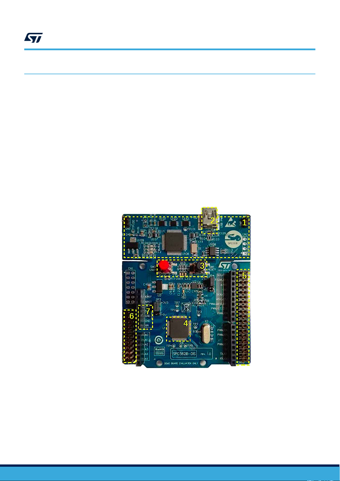
Figure 3. AEK-MCU-C1MLIT1 Discovery board components
1. PLS programmer/debugger
2. USB power connector to supply 5V and load firmware
3. User interface with three LEDs and two buttons
4. 32-bit SPC582B60E1 MCU
5. CN10 19x2 connector for access to I²C and I²S ports and GPIOs
6. CN7 11x2 connector for access to I²S ports and GPIOs
7. CN6 connector allows supplying the board with different external voltage (3.3 V, 5 V or 12 V)
UM2719
UM2719 - Rev 3
The SPC582B60E1 microcontroller includes the following additional features:
• 1088 KB (1024 KB code flash + 64 KB data flash) on-chip flash memory: supports read during program and
erase operations, and multiple blocks allowing EEPROM emulation
• Comprehensive new generation ASIL-B safety concept:
– ASIL-B of ISO 26262 – FCCU for collection and reaction to failure notifications
– Memory Error Management Unit (MEMU) for collection and reporting of error events in memories.
• 1 enhanced 12-bit SAR analog-to-digital converter:
– Up to 27 channels (two channels are used in the AVAS application for sound volume and acceleration)
– enhanced diagnostic feature.
page 3/60
Page 4

UM2719
I²S bus interface on the SPC582B60E1 microcontroller
• I²C interface
4 serial peripheral interface (DSPI) modules (a DSPI is used in the AVAS Demo to simulate the I²S bus
•
interface).
2.1 I²S bus interface on the SPC582B60E1 microcontroller
The FDA903D audio amp receives the audio signal from the flash blocks of the SPC582B60E1 via the I²S bus.
This interface can transmit two different audio channels on the same data line. As SPC5 microcontrollers do not
have a native I²S interface, an emulation through the DSPI protocol is implemented.
2.1.1 I²S protocol details
The I²S bus consists of the following lines:
I2S SCL The clock signal frequency is the product of the sampling frequency and the number of bits
transmitted.
I2S DATA The transmitted data are coded in two's complement, and the MSB (Most Significant Bit) is
therefore in the first position of each word. The data word is composed of 32 bits.
Note: The device only processes the first 24 most significant bits and disregards the least significant 8 bits.
I2S WS The Word Select signal is synchronized with the sampling frequency. Its digital value identifies
the transmission channel (0 = right channel, 1 = left channel).
2.1.2 I²S emulation on DSPI for SPC5 MCU control of FDA903D amplifier
The FDA903D power amplifier allows audio playback at the following sampling frequencies:
•
44.1 kHz
• 48 kHz
• 96 kHz
• 192 kHz
The maximum DSPI clock limit can only support the lowest frequency (fs = 44.1 kHz).
DSPI is a synchronous serial communication interface primarily used for short-distance communication in
embedded systems. This interface is based on four signals:
SCLK: the serial clock signal from the master (the microcontroller in our application)
MOSI: the serial data from the master to the slave (the FDA903D in our case)
MISO: the serial data from the slave to the master
CS: selects which slave chip receives the message from the master
DSPI emulation of the I²S interface is therefore obtained through the following associations and parameter values:
•
I2S DATA → DSPI MOSI
– 32-bit data word
• I2S WS → DSPI CS
– varies the channel (right or left) according to the fs (sampling frequency).
• I2S SCLK → DPSI SCLK
– Frequency = n
= 2.822MHz .
• I2S TEST → DSPI MISO
– This additional signal allows the FDA903D to send real-time current sensing information to the
microcontroller and to a DSP for sound processing.
umberofcℎannels × numberofbitsinaword × samplingfrequency = 2x32x44.1kHz
UM2719 - Rev 3
page 4/60
Page 5

Figure 4. Standard I²S data format
1 / (64 x fs)
I2Sclk
I2Sws
I2SdataLeft channel Right channel
1 / fs
1 / (2 x fs) 1 / (2 x fs)
T
SCK
I2S SCL
I2S CR
I2S SDA
I2S WS
• MCU DSPI0 port access via four CN10 connector pins
• MCU has four DSPI ports
Figure 5. Connector CN10 pins for DSPI0
UM2719
I²S bus interface on the SPC582B60E1 microcontroller
RELATED LINKS
Refer to TN1296: "I²S emulation on DSPI" for more information about emulating the I²S protocol
UM2719 - Rev 3
page 5/60
Page 6

=
=
=
Data
Subaddrs
Address
Address
SubaddressAS A
Data
P
DATA
ADDR
DATA DATA DATA
SUB A
DATA
SUB A
DATA
SUB A
DATA
SUB A
DATA
SUB A
ADDR ADDR
ADDR ADDR ADDR ADDR ADDR
SUB ASUB ASUB A
UM2719
I²C bus interface on the SPC582B60E1 microcontroller
2.2 I²C bus interface on the SPC582B60E1 microcontroller
The I²C interface is used to control, program and request information from the audio amp. Data transmission from
SPC582B60E1 to the FDA903D
and SCL lines.
Note: According to the I²C protocol, it is mandatory to insert pull-up resistors to positive supply voltage on the SDA and
SCL lines.
[S] Start bit
Chip address byte
Sub-address byte
[data] n-byte + Acknowledge bit
[P] Stop bit
and vice versa takes place through the two-wire I²C bus interface for the SDA
Figure 6. I²C typical data format
The AEK-MCU-C1MLIT1 provides I²C port access through two pins on the CN10 connector shown in the figure
.
below
The discovery board has a single dedicated I²C port. Additional ports can be added by emulating the I²C protocol
via software to configure a GPIO pin for I²C SCL and another pin for I²C SDA.
UM2719 - Rev 3
page 6/60
Page 7

I2C SCL
I2C SDA
I²C bus interface on the SPC582B60E1 microcontroller
Figure 7. Connector CN10 pins dedicated to I²C
UM2719
UM2719 - Rev 3
page 7/60
Page 8

UM2719
AEK-AUD-D903V1 evaluation board for automotive power amplifier
3 AEK-AUD-D903V1 evaluation board for automotive power amplifier
The AEK-AUD-D903V1 is designed to allow evaluation and application development based on the embedded
FDA903D automotive digital class D power amplifier in a PowerSSO-36 slug-down package.
Figure 8. AEK-AUD-D903V1 main components and interfaces
1. Output channel; 2. FDA903D power amplifier; 3. Power supply connector
4. Enable and HW mute pins: [EN1 to EN4]: 4 pins can be configured to switch on the amplifier and assign it on of 7 possible an
I²C addresses, [MUTE]: allows MUTE setting control of the power amplifier through a GPIO
5. I²C interface: [I2C SCL]: I2C clock line, [I2C SDA]: I2C data line
6. I²S interface: [I2S SCL]: I2S clock line, [I2S WS]: I2S Word select line, [I2S SDA]: digital input, [I2S CR]: I2S Output test
current, [GND]
2
1
3
4 5 6
The FDA903D power amplifier can be configured through its I²C bus interface and the device includes the
following diagnostics suite designed for automotive applications:
• open load in play detection
• DC diagnostic in MUTE to monitor the load status
• short to V
• digital Input Offset detection
• output Voltage Offset detection
• output Current Offset detection
• thermal protection
The FDA903D features a configurable power limiting function and can be optionally operated in legacy mode
without I²C communication.
/ GND diagnostic
CC
3.1 FDA903D finite state machine
The FDA903D finite state machine (FSM) describes how the device reacts to system and user inputs.
UM2719 - Rev 3
page 8/60
Page 9

Figure 9. FDA903D state machine
Stand By
Diag Vcc/Gnd
ECO-mode
Mute
Diag DC
Dump
Play
Enables set
AND
I2C programmed for the first
time
No short to Vcc/Gnd
condition STABLE for at least
90ms
I2C cmd:
“Diag DC start”
Diagnostic DC end
I2C cmd:
“PLAY”
Vcc over Overvoltage
shutdown limit
Enables = "0000"
OR
Vcc for system reset
OR
90ms Short to Vcc/Gnd check
Short to Vcc/Gnd present
(even for one instant)
I2C cmd:
“PWM ON”
I2C cmd:
“PWM OFF”
I2C cmd: "MUTE"
OR
Automatic mute
condition present
Vcc under
Overvoltage
shutdown limit
Overcurrent protection
OR
UVLO present
OR
Thermal shutdown
UM2719
FDA903D finite state machine
The initial standby state of the device cannot be exited until the I²C interface has been correctly enabled by
providing the correct supply voltage, the I²S clock, the I²S data and a valid combination of enable pins in order to
determine the I²C device address.
Standby
Amplifier ON address 1 = ‘1110000’ 0 1 0 0
Amplifier ON address 2 = ‘1110001’ 1 1 0 0
Amplifier ON address 3 = ‘1110010’ 0 0 1 0
Amplifier ON address 4 = ‘1110011’ 0 1 1 0
Amplifier ON address 5 = ‘1110100’ 0 1 0 1
Amplifier ON address 6 = ‘1110101’ 1 1 0 1
Amplifier ON address 7 = ‘1110110’ 0 0 1 1
Amplifier ON address 8 = ‘1110111’ 0 1 1 1
Configuration
Table 1. I²C device address combinations
Pin
Enable 1 Enable 2 Enable 3 Enable 4
0 0 0 0
UM2719 - Rev 3
page 9/60
Page 10

UM2719
FDA903D I²S protocol
When a valid combination of Enable 1/2/3/4 is recognized, the device turns on all the internal supply voltages
and outputs are biased to VCC
instruction. A return to the Standby condition (all the enable pins set to 0) resets of the amplifier. The finite state
machine shows that a reset is also triggered if PLL is not locked, I²S is missing or not correct, or VCC is removed.
There are also four possible legacy mode combinations for device operation without using the I²C interface.
/ 2. The internal I²C registers are preset in the default condition until the I²C next
Table 2. Legacy mode Enable configurations
Configuration
Legacy mode: low voltage mode; in-phase
Legacy mode: low voltage mode; out-phase 1 1 1 1
Legacy mode: standard voltage mode; in-phase 1 0 0 0
Legacy mode: standard voltage mode; out-phase 1 0 0 1
Enable 1 Enable 2 Enable 3 Enable 4
1 1 1 0
Pins
Note: FDA903D can only work in I²C slave mode; any combination other than those indicated are invalid.
3.1.1 FDA903D FSM state descriptions
Standby The ENABLEx pins set the I²C addresses and start up the system; if ENABLE1/2/3/4 are all
low ("0000"), then the FDA903D is of
consumption is limited.
Diagnostic Vcc-Gnd This state checks the device is in a safe operating condition, with no short to ground (Gnd),
short to VCC, overcurrent, undervoltage (UVLO
to the next Eco-mode if none of these faults occur for at least 90 ms. A stable fault is
communicated to the user via I²C messages after 90 ms. While in Diagnostic Vcc-Gnd state,
FDA903D can receive all the I²C commands but will not turn the PWM on.
ECO-mode The amplifier is fully operational and can receive and execute any valid command. Output
switching is disabled for low power consumption. The device can move from ECO-mode to
the MUTE state in order to activate switching within about 1 ms and without experiencing
POP-noise. This facilitates fast transition from ECO-mode to PLA
MUTE The FSM transitions from ECO-mode to the MUTE state through the I²C command to turn on
PWM. The MUTE state allows quick transition to PLA
PLAY The FSM transitions to this state from MUTE via the I²C “PLAY” command, and the same status
register bit governs the return from PLA
low battery mute, high battery mute, hardware mute pin and thermal mute automatically return
the amplifier to the MUTE state.
Diag DC This state starts the DC diagnostic routine to detect the load connection status and returns to
the MUTE state when the routine has finished.
Note: I²C commands performed by the user are executed via the I²C protocol by modifying the device register settings.
f, the outputs remain biased to ground and the current
), or thermal shutdown. The FDA903D
Vcc
moves
Y.
Y and diagnostic states.
Y back to MUTE. Certain external conditions such as
RELATED LINKS
Refer to the FAD903 datasheet for more information regarding its state machine
3.2 FDA903D I²S protocol
Audio data is transmitted to the power amplifier via the I²S protocol. The 32-bit data word is in two's complement
representation starting from the MSB. The device only processes the first 24 most significant bits and disregards
the 8 least significant bits.
Note:
UM2719 - Rev 3
Besides the standard I²S used in our demo, the FDA903D device also supports Time Division Multiplexing mode
(TDM).
page 10/60
Page 11

I2S CURRENT TEST
UM2719
FDA903D I²C protocol
The FDA903D internal PLL locks on the I²S clock line signal frequency, which is why it is important to configure
the I²S bus appropriately. When the I²S clock is missing or corrupted, the PLL unlocks and the device is forced
into a standby state.
Figure 10. I²S (DSPI) connection in AEK-AUD-D903V1
I2S CLOCK LINE
I2S WS LINE
I2S DATA LINE
3.3 FDA903D I²C protocol
The DATA and SCLK wires for the I²C protocol are used to communicate, control and manage the FDA903D.
Connection between the I²C microcontroller port and I²C power amplifier pins on the AEK-AUD-D903V1 is
provided by the pins on the connector shown below.
UM2719 - Rev 3
page 11/60
Page 12

Figure 11. I²C connection in AEK-AUD-D903V1
I2C CLOCK LINE
I2C DATA LINE
UM2719
FDA903D I²C protocol
The power amplifier FDA903D is controlled with appropriate read and write operations on Instruction Bytes
registers (from IB0 to IB14) performed with the I2C protocol. Additional Data Bytes registers (from DB0 to DB6) in
the device record the state of the amplifier.
Writing to the instruction registers and reading from the device status registers are the fundamental elements of
device management.
3.3.1 I²C protocol writing procedure
Communication through the I²C protocol takes place via a well-defined sequence of bit packages: start bit →
recipient address → acknowledge bit → sub-address → acknowledge bit → actual data → stop bit.
The amplifier address is chosen from eight possible enable pins combinations that represent eight corresponding
addresses. For example, to assign I²C address1 = “1110000” to the device, enable pin 2 is set high (Enable 2 =
“1”) and enable pins 1,3 and 4 are set low (Enable1 = “0”, Enable3 = “0”, Enable4 = “0”).
Configuration
Standby
Amplifier ON address 1 = ‘1110000’ 0 1 0 0
Amplifier ON address 2 = ‘1110001’ 1 1 0 0
Amplifier ON address 3 = ‘1110010’ 0 0 1 0
Amplifier ON address 4 = ‘1110011’ 0 1 1 0
Table 3. I²C address 1 selection
Pin
Enable 1 Enable 2 Enable 3 Enable 4
0 0 0 0
UM2719 - Rev 3
page 12/60
Page 13

ENABLE 1
ENABLE 2
ENABLE 3
ENABLE 4
UM2719
FDA903D I²C protocol
Configuration
Amplifier ON address 5 = ‘1110100’
Amplifier ON address 6 = ‘1110101’ 1 1 0 1
Amplifier ON address 7 = ‘1110110’ 0 0 1 1
Amplifier ON address 8 = ‘1110111’ 0 1 1 1
The connector on the AEK-AUD-D903V1 provide access to the four enable pins by four corresponding GPIO pins
on the microcontroller.
Important: Close J2 connector pins with jumpers.
Figure 12. ENABLE pin locations on the connector
Pin
Enable 1 Enable 2 Enable 3 Enable 4
0 1 0 1
UM2719 - Rev 3
The subaddress is assigned according to the IB register to be written, as shown in the following table.
Table 4. Subaddress association
Register name Corresponding Subaddress
IB0 I0000001
IB1 I0000010
page 13/60
Page 14

UM2719
FDA903D I²C protocol
Register name Corresponding Subaddress
IB2 I0000011
IB3 I0000100
IB4 I0000101
IB5 I0000110
IB6 I0000111
IB7 I0001000
IB8 I0001001
IB9 I0001010
IB10 I0001011
IB11 I0001100
IB12 I0001101
IB13 I0001110
IB14 I0001111
In the above table, bit 7 of the subaddress is the letter “I” to represent the possibility of having an incremental
writing procedure. If the “I” bit is set to 1, the write operation is performed from the corresponding register and all
consecutive ones with a unique flow of data from I²C. The process can involve all registers or can be interrupted
by a stop bit received from I²C.
The data bits carry the actual information required to control the power amplifier.
3.3.2 I²C protocol: reading procedure
The reading procedure consists of the device address (sent by master) and the data (sent by slave).
When a reading procedure is performed, the first register read is the last addressed in a previous access to I²C
peripheral. Hence, the reading of a register is enabled by a write action (a write interrupted after the sub-address
is sent) to specify which register must be read. The following figure shows the complete procedure to read a
specific register where:
1. The master performs a write action by sending only the device address and the subaddress; the
transmission must be interrupted with the stop condition after the subaddress.
2. The master starts a new communication by sending the device address and the FDA903D slave responds
by sending the data bits.
3. The read communication is ended by the master which sends a stop condition preceded by a notacknowledge.
Figure 14. Read operation required data
Alternatively, performing a start immediately after the stop condition can be used to generate the repeated start
condition (Sr), which also keeps busy the I²C bus until the stop is reached.
Figure 13. Read operation packet
UM2719 - Rev 3
Figure 15. Read operation with repeated start condition
page 14/60
Page 15

3.3.3 IB registers in I²C
The microcontroller accesses all amplifier functionality through the IB registers.
T
able 5. IB register map
IB register map
D7 D6 D5 D4 D3 D2 D1 D0
IB0 D7: enable/disable writing on IB registers
D6-D5: enable/disable the I²S standard protocol for transmitting the digital input
D4-D1: choose between right or left channel
DO: select between low voltage and standard voltage modes
IB1 D7-D6: select the I²S WS
D4-D3: select the PWM switching frequency based on the I²S WS value
D2: select between PWM amplifier dithered or not dithered
DO: select between PWM in phase or out of phase
IB2 D7-D6: establish the short to supply diagnostic timing
D4: activate/deactivate the low radiation function
D3-D0: enable and configure the amplifier power limiter
IB3 D5: enable/disable output voltage offset detector
D4: enable/disable input of
D3: enable/disable output current offset detector
D2: enable/disable high pass filter in DAC amplifier DAC
D1: enable/disable noise gating
D0: enable/disable open load in play detection
IB4 D7: enable CDDIAG to report presence of output voltage offset
D6-D4: enable CDDIAG to report temperature warnings
D3: enable CDDIAG to report overcurrent faults
D2: enable CDDIAG to report input of
D1: enable CDDIAG to report short to VCC or to Gnd fault
fset detector
fset
UM2719
FDA903D I²C protocol
D0: enable CDDIAG to report high voltage Mute fault
IB5 D7: enable CDDIAG to report undervoltage fault
D6: enable CDDIAG to report thermal shutdown fault
D5-4: enable CDDIAG to report PWM pulse skipping
IB6 D7-D6: establish MUTE timing setup
D5: select audio signal gain control
D4: choose between standard gain or low gain
IB7 D7-D6: select the diagnostic ramp time
D5-D4: select the diagnostic hold time
D1: choose between data generated on I²S clock falling edge or rising edge
D0: select the current sensing protocol configuration
UM2719 - Rev 3
page 15/60
Page 16

UM2719
FDA903D I²C protocol
IB8 D7-D6: set the full current sensing scale
D5: turn on/of
D4: enable the DC Diagnostic
D3-D1: configure the I²S CR pin
D0: put the amplifier in MUTE/PLAY
IB9 D4: enable/disable the watchdog for word select management
IB10 D7: set short load impedance threshold for DC diagnostic
D6: set open load impedance threshold for DC diagnostic and open load in play
D4-D3: configure the output current of
IB11 D5-D4: select the overcurrent protection level
D3: select between default PWM or PWM Slow slope
IB12 D7: select between standard thermal warning or thermal warning shift - 15 °C
IB13 D6: select whether digital mute is enabled or disabled in PLAY when Start Analog Mute without
thermal warnings occurs
IB14: D4: set feedback on LC filter/Out
D3-D1: configure the LC filter setup
D0: select whether or not setup is programmed via 1²C
f the PWM
fset detector threshold
3.3.4 DB registers in I²C
DB registers allow the microcontroller to monitor the status and operation of the power amplifier.
T
able 6. DB register map
DB register map
D7 D6 D5 D4 D3 D2 D1 D0
DB0 D7: indicates whether an offset at input is present
D6: indicates whether the current of
D5: indicates whether an offset at current offset is present
D3: indicates whether an offset at voltage offset is present
D2: indicates whether the open load in play test has ended
D1: indicates whether the open load in play test is valid
Do: indicates whether an open load is present or not
DB1 D7-D4: indicates whether the thermal warning is active
D3: indicates whether the PLL is locked
D2: indicates whether an undervoltage UVLOALL has been detected
D1: indicates whether an overvoltage shutdown has been detected
D0: indicates whether PWM pulse skipping has been detected
fset test has ended and if it is valid
UM2719 - Rev 3
page 16/60
Page 17

DB2 D7: indicates whether the DC diagnostic pulse has ended
D6: indicates whether the DC diagnostic is valid
D5: indicates whether the overcurrent protection has been activated
D4: indicates when a short load on channel occurs
D3: indicates when a short to V
on channel occurs
CC
D2: indicates when a short to Gnd on channel occurs
D1: indicates when an open load on channel occurs
D0: indicates whether the channel is in MUTE or in PLAY
DB3 Reserved for DC Diagnostic Error codes
DB4 Register is reserved for Channel Current Sensing (1O - 8)
DB5 Register is reserved for Channel Current Sensing (7 - 0)
DB6 D7: indicates whether the high voltage mute has started
D6: indicates whether an undervoltage UVLOV
has been detected
CC
D5: indicates whether a thermal shutdown has been detected
D4: indicates whether the analog mute is started
D2: indicates whether the watchdog for word select occurs
D1: indicates whether an error frame occurs
UM2719
Potentiometers
3.3.5 Driver
A driver has been developed to allow the user to monitor and control the amplifier without engaging in tedious IB
and DB register read and write operations associated with a task.
3.4 Potentiometers
The AVAS system includes two potentiometers to help simulate the sound of a car engine: one to simulate the
accelerator pedal and another to adjust the sound volume. The potentiometers are powered through two supply
voltages (5V and 3.3V) from the AEK-MCU-C1MLIT1 control board via female connector CN6 or male connector
CN7.
Our system uses the potentiometer as a voltage divider to obtain a manually adjustable output voltage from
a fixed input voltage applied across the two ends of the potentiometer. It is formed by an insulating cylinder
on which a metal wire is wound, and the two ends are connected to two terminals. One of these terminals is
connected to a sliding contact that runs the length of the cylinder. The operation is equivalent to a pair of resistors
in series whose total value is constant, but individually variable according to the position of the sliding contact.
Figure 16. Linear potentiometer circuit
UM2719 - Rev 3
Considering RL an open, we have the voltage on RT2 equal to the power supply voltage of the potentiometer
multiplied by
2
, and since this ratio is equal to that of LT2 (R
resistor length) on LT (total resistor length), we
T2
see that the output voltage of the potentiometer is a function of the cursor position.
page 17/60
Page 18

Successive approximation analog-to-digital converter (SARADC)
V*L
V2=
T2
L
T
It is possible to implement speed and volume control by directly relating these variables to the output voltage of a
potentiometer
. The analog output of the potentiometers are converted into discrete values by the SPC582B60E1
microcontroller ADCs.
3.5 Successive approximation analog-to-digital converter (SARADC)
Two of the 27 SARADC channels on the AEK-MCU-C1MLIT1 control board microcontroller are used to convert
the potentiometer speed and volume signals into digital quantities through the connector CN7.
Note:
These signals can also be routed through CN11.
Figure 17. Potentiometer connections
UM2719
(1)
3.6 Stereo mode
In order to produce stereo audio, the system requires a second AEK-AUD-D903V1 board to occupy both the left
and right channels available on the I²S DA
UM2719 - Rev 3
TA line.
page 18/60
Page 19

UM2719
Stereo mode
Figure 18. A
VAS system for two stereo sound
The connection of a second audio board will involve the following modifications to the AVAS system:
The I²C interface is shared, so the I2C SCL clock line and the I2C DATA line are connected to both
•
AEK-AUD-D903V1 audio boards.
• The I²S interface is also shared as the lines (I2S SCLK, I2S WS and I2S DATA) are also used by the second
amp. The right channel and the left channel travel on the same line, and the I2S WS distinguishes the
information for the right channel and the left channel.
• The I²C communication between the microcontroller (master) and the two amplifiers (slaves) are
distinguished by the addresses that identify the two devices.
• The address that identifies each of the two amplifiers is obtained through a combination of the four enables,
so eight GPIOs are required in total.
This AEK-MCU-C1MLIT1 control board has a copy of the male CN7 and CN10 connectors on the back of the
board, which makes it relatively easy to split the connections for the I²C and I²S interfaces between the two amps.
UM2719 - Rev 3
page 19/60
Page 20

UM2719
Stereo mode
Figure 19. AEK-MCU-C1MLIT1 seen on both sides
Even though it would normally take eight GPIOs to assign addresses to the two amplifiers, we can use the copy
of the connectors on the back side of the control board to halve the number of GPIOs. T
combinations that have the same number of pins to put high ("1").
o do this, we use two
Table 7. Comparison of pin settings for addresses 1 and 3
Configuration
Amplifier ON address 1 = ‘1110000’
Amplifier ON address 3 = ‘1110010’ 0 0 1 0
Enable 1 Enable 2 Enable 3 Enable 4
0 1 0 0
Pin
In the above example, where address 1 and address 3 have the same number of high and low pins, it is evident
that we can use the same GPIOs to create the two necessary combinations by connecting the GPIO high (“1”)
to Enable 2 of the first board and Enable 3 of the second board, and the three low GPIOs (“0”) to the remaining
three enable pins on each board.
UM2719 - Rev 3
page 20/60
Page 21

AEK-AUD-C1D9031 - single board AVAS solution
4 AEK-AUD-C1D9031 - single board AVAS solution
The AEK-AUD-C1D9031 is a very compact AVAS solution based on SPC582B60E1 Chorus family MCU and
FDA903D Class D audio amplifiers that emits warning sounds to alert pedestrians of the presence of e-vehicles in
the proximity.
The optimized board size allows installation of more than one AVAS module in an e-car to guarantee that the
warning sound is heard in any direction along the vehicle.
4.1 Hardware overview
Figure 20. AEK-AUD-C1D9031 components
1. SPC582B60E1 automotive microcontroller
2. Class D FDA903D power amplifiers
3. CAN connector
4. Hardware mute switch
5. Turn on/off sound button
6. Connector compatible with AEK-CON-C1D9031
UM2719
UM2719 - Rev 3
The board hosts the SPC582B60E1 automotive microcontroller belonging to the Chorus family, embedding a high
performance e200z2 single core 32-bit CPU with 80 MHz clock, 1088 KB Flash and 96 KB SRAM, in a compact
eTQFP64 package.
The microcontroller monitors and controls the two Class D FDA903D power amplifiers driving the loudspeakers.
The audio transmission from the microcontroller to the two audio amplifiers is implemented via I²S interface
(simulated by an SPI peripheral), while I²C port and GPIOs are used to provide the necessary signals and
communication lines to configure the power amplifiers.
The proposed AVAS solution is designed to be remotely controlled by a central ECU via CAN interface, using the
on-board CAN connector. The board also features a hardware mute button and a button to turn on/off the sound.
A connector is present as well for two sliders: one to manage the speed (engine rpm) and the other to manage
the volume. A compatible version of these sliders is included in the AEK-CON-C1D9031.
page 21/60
Page 22

UM2719
Software overview
4.2 Software overview
The board is ready to be tested. An example of firmware has been already uploaded on it.
If you need to download the firmware into the board again, use SPC5-UDESTK programmer plugged on the JT
connector. The source code is present from AutoDevKit 1.4.0, i.e. a specific demo has been implemented for this
board, “SPC582Bxx_RLA_AEK_AUD_C1D9031 - Avas Compact - Test Application”. To upload the demo into the
microcontroller, refer to Section 7.2.1 How to upload the demos for AEK-AUD-D903V1.
The demo provides an example of how to manage the two FDA903D audio amplifiers with a driver dedicated
to an AEK-AUD-C1D9031 board. The demo shows how to simulate car engine sound, performing diagnostic in
real-time, in two different states: PLAY and MUTE. The detection of the open load in play mode depends on the
sound characteristics (refer to the FDA903D datasheet for details).
To Start and Stop the sound, use the dedicated button shown in Figure 20. While in Stop status, the LED D6
turns on. When the open load fault is detected, LED D8 turns on, while LED D7 is turned on when pushing the
hardware Mute button.
By default, this demo is controlled via CAN by an external MCU/ECU. In addition, it is possible to simulate the
car engine acceleration/deceleration using commands via CAN. The file CANCommunication.h under the source
folder contains the information (SID and Value) related to the messages managed by the demo.
To receive CAN diagnostic messages from the demo, it is mandatory to set the variable
DISTRIBUTED_AVAS_SYSTEM in the main.c as follows:
#define DISTRIBUTED_AVAS_SYSTEM TRUE
The CAN messages will be sent out by the demo to the main ECU in case of open load in play or in mute state.
The sound produced is based on .hex files located under the source/SamplePack folder and have to be loaded
into the Flash memory. A simple Flash memory loading procedure is described in Section 6.2 from step 21 on.
In this demo, we have used a simple algorithm that, depending on the rpm detected, skips some of the wave file
samples to simulate the engine acceleration/deceleration.
Note: It is possible to simulate the car engine acceleration/deceleration and the volume by using two trimmers from
AEK-CON-C1D9031 and changing the ENABLESLIDER variable in the main.c file from
#define ENABLESLIDER FALSE
to
#define ENABLESLIDER TRUE
AG
Important:
Free UDE license allows loading 256 Kb max. To get a full license, you can buy SPC5-UDESTK programmer together with
SPC5-UDEDEBG-TL
unlimited code-size license.
for a one-year, full-feature, unlimited code-size license or SPC5-UDEDEBG for a perpetual, full-feature,
4.3 FCC and IC disclaimer
FCC notice:
This device complies with part 15 of the FCC Rules. Operation is subject to the following two conditions: (1) This
device may not cause harmful interference, and (2) this device must accept any interference received, including
interference that may cause undesired operation. Changes or modifications not expressly approved by the party
responsible for compliance could void the user's authority to operate the equipment. Note: This equipment has
been tested and found to comply with the limits for a Class A digital device, pursuant to Part 15 of the FCC Rules.
These limits are designed to provide reasonable protection against harmful interference when the equipment is
operated in a commercial environment. This equipment generates, uses, and can radiate radio frequency energy
and if it is not installed and used in accordance with the instruction manual, it may cause harmful interference to
radio communications. Operation of this equipment in a residential area is likely to cause harmful interference, in
which case the user will be required to correct the interference at his own expense.
IC notice:
This Class A digital apparatus complies with Canadian ICES-003. Cet appareil numérique de la classe A est
conforme à la norme NMB-003 du Canada.
,
UM2719 - Rev 3
page 22/60
Page 23

5 AVAS system software
The AVAS demo system requires the following set of software tools to develop and load the microcontroller
firmware to drive and monitor the power amplifier:
• SPC5-STUDIO
• STSW-AUTODEVKIT
• AEK-AUD-D903V1 driver
RELATED LINKS
Refer to user manual UM2623 for more information regarding SPC5-STUDIO and STSW-AUTODEVKIT
5.1 SPC5-STUDIO
SPC5-STUDIO is an integrated development environment (IDE) based on Eclipse designed to assist the
development of embedded applications based on SPC5 Power Architecture 32-bit microcontrollers.
The package includes an application wizard to initiate projects with all the relevant components and key elements
required to generate the final application source code. It also contains straightforward software examples for each
MCU peripheral.
Other advantages of SPC5-STUDIO include:
•
ability to integrate other software products from the standard Eclipse marketplace
• free license GCC GNU C Compiler component
• support for industry-standard compilers
• support for multi-core microcontrollers
• PinMap editor to facilitate MCU pin configuration
and SPC5-UDESTK-SW debugger
UM2719
AVAS system software
RELATED LINKS
Download the SPC5-UDESTK-SW software to run and debug applications created with SPC5-STUDIO
5.2 STSW-AUTODEVKIT
The STSW
The main advantages of STSW-AUTODEVKIT are:
• integrated hardware and software components, component compatibility checking and MCU and peripheral
• allows creation of new system solutions from existing solutions by adding or removing compatible function
• Hardware abstraction means new code can be generated immediately for any compatible MCU
• High-level application APIs to control the AEK-AUD-D903V1 board.
The GUI helps configure interfaces, including I²C and I²S, and can automatically manage all relevant pin
allocation and deallocation operations.
-AUTODEVKIT plug-in for Eclipse extends SPC5-STUDIO for automotive applications.
configuration tools
boards
5.3 AEK-AUD-D903V1.c and sound.c drivers
The AEK-AUD-D903V1.c driver and sound.c library are provided with the STSW
facilitate the programming phase.
5.3.1 AEK-AUD-D903V1.c driver
This driver contains the functions to configure the IB and DB registers of the FDA903D audio amplifier for
appropriate system management and control.
Consider the IB8 register below
.
-AUTODEVKIT installation to
UM2719 - Rev 3
page 23/60
Page 24

AEK-AUD-D903V1.c and sound.c drivers
Table 8. FDA903D IB8 register description
UM2719
Data bit Default value
D7-D6 11
D5 0
D4 0
D3-D1 000
D0 0
Definition
Bit value Effect
Current Sensing Full scale setting:
0
1
10
11
0 Channel in TRISTATE (PWM OFF)
1 Channel with PWM ON
0 Channel DC Diag disable
1 Channel DC Diag start
000 High impedance configuration
001 Reserved
010 Reserved
011 Output: Current sensing enable
100 Reserved
101 Output: PWM synchronization signal
110 Reserved
111 Reserved
0 Channel in MUTE
1 Channel in PLAY
1 A I
2 A I
4 A I
8 A I
max
max
max
max
I²S test pin configuration
To put the amplifier in PLAY mode, we need to configure the register accordingly:
turn on the PWM setting IB8[D5] = 1
•
• put the channel in play setting IB8[D0] = 1
The Initial state is the default 11000000. To reach the state PWM on state, we compute 11000000 OR 00100000
to obtain 11100000. To reach the PLAY mode state, we perform 11100000 OR 0001000 to obtain 11110000.
It takes several operations to modify the relevant bits in the IB register in order to transmit a simple instruction to
the amplifier.
The AEK-AUD-D903V1.c simplifies these operations through a list of APIs that can configure the IB registers in a
single command.
For example, the AEK_903D_Play(AEK_AUD_D903V0) function configures the IB8 register bits required to set
the amplifier in PLAY mode.
Note: The parameter of the function indicates the name of the amplifier to control, so in a stereo system with two audio
boards, we must distinguish between AEK-AUD-D903V0 and AEK-AUD-D903V1.
UM2719 - Rev 3
page 24/60
Page 25

AEK-AUD-D903V1.c and sound.c drivers
Figure 21. API AEK_903D_Play(AEK_AUD_D903V0)
1. The function saves the current state of the IB8 register to the variable FDA903D_Status_IB
2. The function changes the value of variable FDA903D_Status_IB to turn on PWM and activate PLAY mode.
3. The function writes the value of the
PLAY mode.
FDA903D_Status_IB variable to the IB8 register, effectively setting the amplifier in
1
UM2719
2
3
Some APIs in the AEK-AUD-D903V1.c driver require specific configuration parameters. In the following example,
bits D3, D2 and D1 combine to define different configurations (000 = high impedance configuration, 011 = current
sensing configuration, etc.). This API therefore requires indication of the desired configuration as well as the
relevant device when it is invoked.
Figure 22. I2S Test Pin configuration API
1. The user must replace the description with the appropriate value field to indicate the desired configuration.
1
UM2719 - Rev 3
The following table shows all the available functions divided according to the register on which they act.
page 25/60
Page 26

Table 9. list of API functions in AEK-AUD-D903V1.c
Register API
AEK_903D_EnableWritingOnlBs
AEK_903D_DisableWritingOnlBs
IB0
IB1
IB2
IB3
IB4
IB5
AEK_903D_SetlnputDataFormats
AEK_903D_SelectChannelPosition
AEK_903D_SetVoltageMode
AEK_903D_SetI2SWordSelect
AEK_903D_SetPWMSwitchingFrequency
AEK_903D_SetPwmAplifierDithered
AEK_903D_SetPwmAplifierNotDithered
AEK_903D_SetPwmlnPhase
AEK_903D_SetPwmOutOfPhase
AEK_903D_SetDiagShort2SupplyTiming
AEK_903D_DisableLowRadiationFunction
AEK_903D_EnableLowRadiationFunction
AEK_903D_ConfigurePowerLimit
AEK_903D_DisableOutputVoltageOffsetDetector
AEK_903D_EnableOutputVoltageOffsetDetector
AEK_903D_DisablelnputOffsetDetector
AEK_903D_EnablelnputOffsetDetector
AEK_903D_DisableOutputOffsetCurrentDetector
AEK_903D_TriggerOutputOffsetCurrentDetector
AEK_903D_DisableHighPasslnDAC
AEK_903D_EnableHighPasslnDAC
AEK_903D_DisableNoiseGating
AEK_903D_EnableNoiseGating
AEK_903D_DisableOpenLoadlnPlayDetection
AEK_903D_TriggerOpenLoadlnPlayDetection
AEK_903D_EnableOutputVoltageOffsetInfoOnCDDIAG
AEK_903D_DisableOutputVoltageOffsetlnfoOnCDDIAG
AEK_903D_ConfigureThermalWarninglnfoOnCDDIAG
AEK_903D_EnableOvercurrentlnfoOnCDDIAG
AEK_903D_DisableOvercurrentlnfoOnCDDIAG
AEK_903D_EnablelnputOffsetlnfoOnCDDIAG
AEK_903D_DisablelnputOffsetlnfoOnCDDIAG
AEK_903D_EnableShortToVccOrGndlnfoOnCDDIAG
AEK_903D_DisableShortToVccOrGndlnfoOnCDDIAG
AEK_903D_EnableHighVoltageMutelnfoOnCDDIAG
AEK_903D_DisableHighVoltageMutelnfoOnCDDIAG
AEK_903D_EnableUvlovcclnfoOnCDDIAG
AEK_903D_DisableUvlovcclnfoOnCDDIAG
UM2719
AEK-AUD-D903V1.c and sound.c drivers
UM2719 - Rev 3
page 26/60
Page 27

Register API
AEK_903D_EnableThermalShutdownlnfoOnCDDIAG
IB5
IB6
IB7
IB8
IB9
IB10
IB11
IB12 AEK_903D_SetThermalWarning
IB13
IB14
AEK_903D_DisableThermalShutdownlnfoOnCDDIAG
AEK_903D_EnablePwmPulseSkippinglnfoOnCDDIAG
AEK_903D_DisablePwmPulseSkippinglnfoOnCDDIAG
AEK_903D_SelectMuteTimingsetup
AEK_903D_SelectAudioSignalGainControl
AEK_903D_SelectGainSetting
AEK_903D_SelectDiagnosticRampTime
AEK_903D_SelectDiagnosticHoldTime
AEK_903D_SelectCurrentSensingCommunication
AEK_903D_SelectCurrentSensingProtocolConfiguration
AEK_903D_SetCurrentSensingFullScale
AEK_903D_SetChannelWithPWMoff
AEK_903D_SetChannelWithPWMon
AEK_903D_Eco_Mode
AEK_903D_StartDCDiag
AEK_903D_DisableDCDiag
AEK_903D_I2TestPinConfiguration
AEK_903D_Play
AEK_903D_Mute
AEK_903D_EnableWatchDogForWordSelect
AEK_903D_DisableWatchDogForWordSelect
AEK_903D_SetShortLoadlmpedanceThreshold
AEK_903D_SetOpenLoadlmpedanceThreshold
AEK_903D_SetCurrentOffsetThreshold
AEK_903D_SelectOverCurrentProtectionLevel
AEK_903D_SetSlowSlopePWMConfiguration
AEK_903D_SetDefaultPWMConfiguration
AEK_903D_EnableDigitalMutelnPlayForTW1
AEK_903D_DisableDigitalMutelnPlayForTW1
AEK_903D_SetFeedbackOnLCFilter
AEK_903D_SetFeedbackOnOutPin
AEK_903D_SetupLCFilter
AEK_903D_Enable903ToBeProgramVial2C
AEK_9030_Disable903ToBeProgramVial2C
UM2719
AEK-AUD-D903V1.c and sound.c drivers
Other functions in AEK-AUD-D903V1.c that are not register specific are listed below:
AEK_903D_Write_IB: I²C write to IB registers
AEK_903D_Read_IB: I²C read of single IB register
AEK_903D_Read_All_IB: I²C read of all IB registers
UM2719 - Rev 3
page 27/60
Page 28

UM2719
AEK-AUD-D903V1.c and sound.c drivers
AEK_903D_Read_DB: I²C read of single DB register
AEK_903D_Read_All_DB: I²C read of all DB registers
AEK_903D_SetDefaultRegi
sters:
AEK_903D_SetEnables: used inside the AEK_903D_Init function to set/clear the Enable pins of the board as defined in
AEK_903D_Init: initializes the I²C and I²S protocol and to launch the AEK_903D_SetEnables function
AEK_903D_I2C_Init: initializes the I²C peripheral
AEK_903D_I2S_Init: initializes the I²S peripheral
AEK_903D_CheckOpenLoa
dInPlayDetection:
initializes I²C registers in AEK-AUD-D903V1 and sets first bit of IB14 to 1 (ready to work)
the configuration
returns the result of the Open Load in Play Detection test on the DB0 register in the
FDA903D_Errors structure
AEK_903D_CheckOffsetCu
rrent:
AEK_903D_CheckInputOffs
etDetector:
AEK_903D_CheckOutputVo
ltageOffsetDetector:
AEK_903D_CheckDCDiagn
returns the result of the Current Offset detection test on the DB0 register in the
FDA903D_Errors structure
returns the result of the Input Offset Detection test on the DB0 register in the
FDA903D_Errors structure
returns the result of the Output Voltage Offset Detection test on the DB0 register in the
FDA903D_Errors structure
returns the result of the DC Diagnostic on the DB1 register in the FDA903D_Errors structure
ostic:
AEK_903D_Diagnostic: reads the DB register and signals whether a certain failure condition has occurred
(SHOR
T2VCC, SHORT2GND, OVERCURRENT, UNDERVOLTAGE, OVERTEMPERATURE
OVERVOLTAGE) in the FDA903D_Errors structure
5.3.2 sound.c description
This library contains APIs for the generation, reproduction and simulation of audio wave signals.
initWaveFile: This function takes as input the start address of the first WAV file and the number of files
that you intend to load into memory (maximum number dim=10) and initializes the sound_db
structure with all the necessary addresses to identify the beginning and end of each W
getStartWavFile: This function computes the address that points to the first audio sample of a given WAV file.
Y
ou must provide the function with an integer that identifies the location of the WAV file within
the sound_db structure previously initialized by the initWaveFile function.
getHalfWavFile: This function computes the address that points to the middle audio sample of a given WAV file.
ou must provide this function with an integer that identifies the location of the WAV file within
Y
the sound_db structure previously initialized by the initWaveFile function.
AV file.
GetEndWavFile: This function computes the address that points to the last audio sample of a given WAV file.
ou must provide this function with an integer that identifies the location of the WAV file within
Y
the sound_db structure previously initialized by the initWaveFile function.
swapEndian32: This function swaps the order of the bits: from little (big) endian to big (little) endian.
validate_wav_file: This function validates the WAV file by checking the WAV file descriptor parameters.
checkWavFile: This function checks the WAV file and identifies the start, middle and end of each WAV file,
removing the W
AV file header.
load_channel_data: This function loads new data to the transmission buffer.
playSound: This function plays the sample provided in MONO mode by taking as input a pointer to function
that generates the audio samples and an integer indicating the volume.
playSoundStereo: This function plays the sample provided in STEREO mode by taking as input a pointer to
function that generates the audio samples and an integer indicating the volume.
UM2719 - Rev 3
page 28/60
Page 29

UM2719
AEK-AUD-D903V1.c and sound.c drivers
The last two functions deal with actual sound reproduction. Since these two functions work in the same way, with
the only difference being that one plays mono WAV files and the other stereo files, we will describe how the first
one works.
Figure 23. playSound API
1. This input is a function pointer to the sample that playSound will run. The pointer must refer to the user function, which must
return a
2. In this MONO mode example, the same sample is transmitted to both channels. In STEREO mode, the samples for the left
and right channels may differ.
uint32_t data type that is assigned to the variable to be transmitted.
1
2
The sound.c library allows storing samples generated by mathematical functions or writing a function able to
take audio samples from any file WAV loaded in memory.
UM2719 - Rev 3
page 29/60
Page 30

6 How to play an audio WAV file
6.1 SPC582B60E1 memory map
Excluding the 64 KB data flash, the remaining 1024 KB MCU memory is divided into the following blocks:
•
4 blocks of 16 KB (Low Flash Blocks)
• 2 blocks of 32 KB (Low Flash Blocks)
• 2 blocks of 64 KB (Mid Flash Blocks)
• 6 blocks of 128 KB (Large Flash Blocks)
We allocate the Low and Mid Flash Blocks to load and execute the source code of our application, and the
remaining 6 Large Flash Blocks for the WAV audio files. This of course means that the WAV files cannot exceed
768 KB.
The following microcontroller Flash memory map shows the physical addresses used to identify and divide the
different memory portions.
Table 10. Flash memory map of SPC582B
UM2719
How to play an audio WAV file
Start address End address Description
Data Flash: 64 KB
0x00804000 0x00807FFF 16 KB EEPR0M block1 1
0x00808000 0x0080BFFF 16 KB EEPR0M block2 1
0x0080C000 0x0080FFFF 16 KB EEPR0M block3 1
0x00810000 0x00FBFFFF Reserved
Low & Mid Flash blocks: 256 KB for application code
0x00FC0000 0x00FC3FFF 16 KB Code Flash block1 0
0x00FC4000 0x00FC7FFF 16 KB Code Flash block2 0
0x00FC8000 0x00FCBFFF 16 KB Code Flash block3 0
0x00FCC000 0x00FCFFFF 16 KB Code Flash block4 0
0x00FD0000 0x00FD7FFF 32 KB Code Flash block0 0
0x00FD8000 0x00FDFFFF 32 KB Code Flash block1 0
0x00F E0000 0x00FEFFFF 64 KB Code Flash block0 0
0x00FF0000 0x00FFFFFF 64 KB Code Flash block1 0
Large Flash Blocks: 768 KB for audio WAV files
0x01000000 0x101FFFF 128 KB Code Flash block0 0
0x01020000 0x103FFFF 128 KB Code Flash block1 0
0x01040000 0x0105FFFF 128 KB Code Flash block2 0
0x01060000 0x0107FFFF 128 KB Code Flash block3 0
0x01080000 0x0109FFFF 128 KB Code Flash block4 0
0x010A0000 0x010BFFFF 128 KB Code Flash block5 0
0x010C0000 0x0FFFFFFF Reserved
1 RWR partition
RWW Partition ID
6.2 Uploading audio WAV file
Use the procedure below to upload audio WAV files.
UM2719 - Rev 3
page 30/60
Page 31

UM2719
Uploading audio WAV file
Step 1. Launch SPC5-STUDIO and Create a new SPC5-STUDIO application for Chorus 1M (SPC582B).
Step 2. Right-click the [source] folder to create another folder inside it.
ou can name the folder “audio files”.
Y
Step 3. Copy the desired WAV files and paste them inside the newly created folder.
Verify that all files have been inserted.
Figure 24. Project folder for audio files
Step 4. Compile your application.
This creates a file named application.ld in your project folder
.
Step 5. In the same folder, make a copy of the application.ld file and rename the file according to the
compiler you are using.
– Free GCC → user_freegcc.ld.
– Green Hills → user_ghs.ld.
– Hitech → user_hightec.ld.
Step 6. Double click on the user_freegcc.ld file to open it.
UM2719 - Rev 3
page 31/60
Page 32

UM2719
Uploading audio WAV file
Step 7. Inside the file, modify the memory partition by splitting the flash block into flash and sound blocks.
– The new flash block is 256 KB where application source code is loaded and executed
– The new sound block is 768 KB where audio WAV files are saved
Figure 25. Old flash block memory allocation
1. Old 1 MB flash block
1
1. New 256 KB flash block
2. New 768 KB sound block
Figure 26. New flash block memory allocation
1
2
UM2719 - Rev 3
page 32/60
Page 33

Step 8. Define a section called sounddb as indicated below.
Figure 27. sounddb definition
1. Location of new sounddb definition
2. sounddb definition code
1
UM2719
Uploading audio WAV file
2
Step 9. Right-click the [source] folder to create a new file called sounddb.s.
UM2719 - Rev 3
page 33/60
Page 34

UM2719
Uploading audio WAV file
Step 10. In the file, indicate the path of the WAV files to be loaded and declare the variables that identify the
physical start and end addresses of the various WAV files.
Below is an example with paths and address variables for six WAV files.
Figure 28. sounddb.s audio file declarations
1. first line of code
2. start address variable for first audio file
3. end address variable for first audio file
4. path to first audio file
1
2
3
4
UM2719 - Rev 3
page 34/60
Page 35

Step 11. Recompile the project.
The size of the build output should now include the audio files added in the sounddb.s file.
After compiling, the [build] folder will contain the output file of the application in BIN, DMP, ELF, HEX,
MAP and MOT formats.
Figure 29. Build output before adding sounddb.s component
1. size of build output before adding sounddb.s component
UM2719
Uploading audio WAV file
1
Figure 30. Build output after adding sounddb.s component
1. added sounddb.s component
2. size of build output after adding sounddb.s component
1
2
UM2719 - Rev 3
Step 12. Expand the [build] folder, select the out.hex file and move or copy it to the same folder where the
audio files were saved.
The .hex file can actually be saved to any external folder.
page 35/60
Page 36

Step 13. Rename the .hex file as you prefer.
This file contains all the application files.
Step 14. Open your .hex file using a text editor.
You can use the SPC5-STUDIO editor or an external one.
Figure 31. Open hex file with editor
UM2719
Uploading audio WAV file
UM2719 - Rev 3
page 36/60
Page 37

Step 15. Examine the file and verify that the address is 0200000400FCFE.
00FC is the base address (the first 16 bits) of the physical address of the data contained in each
record.
Figure 32. hex file data
Legend:
: start code,
end of file, 04 Extended linear address for 32-bit addressing, etc.),
number of bytes in data field , address of data added to base address, record type (00 data, 01
data 32 hex digits, checksum
UM2719
Uploading audio WAV file
UM2719 - Rev 3
page 37/60
Page 38

Step 16. In the text editor, search for the string following: 020000040100.
This string contains the base address of the sound partition in the memory where the audio WAV
samples specified in sounddb.s are loaded. The sound partition was defined previously in the
user_freegcc.ld file.
Figure 33. Starting point of audio content in hex file
1. search string to find
2. string found in hex file
UM2719
Uploading audio WAV file
1
2
Step 17. Delete all the lines in the hex file before the starting line of the audio content.
The hex file now only contains the sample audio data to be played by the AVAS system.
UM2719 - Rev 3
page 38/60
Page 39

Uploading audio WAV file
Step 18. Open the soundb.s file and remove or comment out all paths to the audio sample files.
This ensures that the application does not include the audio content the next time you compile, leaving
only the information regarding the source code.
Figure 34. sounddb.s file with audio sample file paths removed
1. path statements to be commented or deleted
2. build file returns to its original size when the audio content is removed
1
1
1
UM2719
1
1
1
2
Step 19. Recompile the project.
Step 20. Connect the mini-B USB port on the Discovery AEK-MCU-C1MLIT1 control board to a USB port on
your PC with an appropriate mini USB to USB cable.
UM2719 - Rev 3
page 39/60
Page 40

Step 21. Launch SPC5-UDESTK-SW on your PC and run the debug.wsx file.
This opens a [Multicore / multi program loader] window.
Figure 35. SPC5-UDESTK-SW software with loader window
1. loader window
2. browse file icon
3. remove file icon
UM2719
Uploading audio WAV file
213
Step 22. Click on the [delete] icon in the menu bar to remove the current file from the [Load File To].
Step 23. Click on the [browse] icon to add a new file.
Step 24. Browse to you hex file and select [open].
The [Multicore / multi program loader] window reopens with the hex file in the [Load File To] list.
UM2719 - Rev 3
page 40/60
Page 41

Step 25. Click [OK] to open the [FLASH/OTP Memory Programming Tool] window.
Note: The free UDE license allows you to upload a maximum file size of up to 256 KB.
Figure 36. FLASH/OTP Memory Programming Tool
UM2719
Uploading audio WAV file
Step 26. Select the [Erase] button.
A Flash selection window appears.
Step 27. Select from memory block 8 (0x01000000) to block13 and click [Start].
Figure 37. UDE Flash erase tool
1. blocks to be erased
2. start erase procedure
3. exit when erase has completed
2
1
Step 28. Click [Exit] when the process has finished.
3
UM2719 - Rev 3
Step 29. In the FLASH/OTP Memory Programming Tool, click on [Program All].
This process loads the audio samples.
Step 30. Wait until the operation has completed and select [Exit].
Step 31. Close UDE-STK.
You have loaded your audio samples into the designated memory portion.
page 41/60
Page 42

UM2719
Uploading audio WAV file
Step 32. Save your SPC5-STUDIO application and keep the user.ld and sounddb.s files in a folder
These two files are important because they are the starting point for the creation of the AEK-AUDD903V1 application.
.
UM2719 - Rev 3
page 42/60
Page 43

7 AEK-AUD-D903V1 sample applications
7.1 How to create a simple AEK-AUD-D903V1 application
Before you start, ensure that the audio samples have been correctly loaded in the microcontroller memory.
This procedure shows you how to play an audio WAV file loaded in memory and perform some diagnostics.
Step 1. Create a new SPC5-STUDIO application for the SPC582B series microcontroller and add the following
components:
– SPC582Bxx Init Package Component RLA
– SPC582Bxx Low Level Drivers Component RLA
These components must be added immediately, or the remaining will not be visible.
Step 2. Add the following further components:
– AutoDevKit Init Package Component
– SPC582Bxx Platform Component RLA
– AEK-AUD-D903V1 Component RLA
Figure 38. SPC5-STUDIO adding audio project components
1. SPC582Bxx Platform Component RLA
2. Open available components
3. AEK-AUD-D903V1 Component RLA
UM2719
AEK-AUD-D903V1 sample applications
2
1
3
Step 3. Select [AEK-AUD-D903V1 Component RLA] to open the [Application Configuration] window.
UM2719 - Rev 3
page 43/60
Page 44

UM2719
How to create a simple AEK-AUD-D903V1 application
Step 4. Select the I2S (DSPI) port and the I2S WS. Then, click on [+] to add a new element to the AEK AUD
D903V1 list.
If you want to create a STEREO version, you will need to insert a second element in the list.
Figure 39. AEK-AUD-D903V1 component configuration
1. AEK-AUD-D903V1 component
2. Pin association
3. add new element icon
4. new entry
1
2
4
Step 5. Double click on the newly added element to configure the I²C interface.
The I²C configuration window opens.
3
UM2719 - Rev 3
page 44/60
Page 45

UM2719
How to create a simple AEK-AUD-D903V1 application
Step 6. Select the I²C HW and the address for the power amplifier derived from a combination of enable pins.
To create a STEREO version, you need to assign two different addresses for the two elements so that
you can communicate with each power amplifier independently.
Figure 40. AEK-AUD-D903V1 I²C configuration
1. I2C HW selection
2. Enable pin configuration
3. Confirm configuration
3
1
2
Step 7. Click the [Allocation] button below the AEK-AUD-D903V1 list and click [OK] in the confirmation
window.
This operation delegates automatic pin allocation to STSW-AUTODEVKIT. If the system warns you that
the selected I²S (DSPI) port is not available, restart from step 3 and select another I²S port or another
I²S WS.
UM2719 - Rev 3
page 45/60
Page 46

How to create a simple AEK-AUD-D903V1 application
Step 8. Click on the PinMap editor icon to check that the twelve required pins have been allocated
appropriately.
– I2S SCL (pin 24 → PG11)
– I2S SDA1 (pin 48 → PD5)
– I2S WS (pin 29 → PB11)
– I2S CR (pin 26 → PD11), not used in this application
– I²C SCL (pin 32 → PB8)
– I²C SDA (pin 31 → PB9)
– 4 GPIO pins for Enable
– 1 GPIO pin for Hardware Mute
– 1 GPIO pin for CDDIAG, not used in this application
Figure 41. PinMap editor
1. PinMap editor icon
UM2719
Step 9. Close the PinMap Editor and save the application.
Step 10. Generate and build the application using the appropriate icons in SPC5-STUDIO.
The project folder will be populated with new files, including main.c and the components folder with
AEK-AUD-D903V1 and sound drivers.
Step 11. Before starting coding, insert the user_freegcc.ld and sounddb.s files prepared previously.
1
UM2719 - Rev 3
page 46/60
Page 47

How to create a simple AEK-AUD-D903V1 application
Step 12. Open the main.c file and include AEK-AUD-D903V1 and sound files, and define the required
constants and variables.
#include "components.h"
#include "sound.h"
#include "AEK-AUD-D903V1.h"
/*************** variables section ***************/
extern uint32_t* engine_start1;
/* These variables are defined in the file sounddb.s,
thus it is necessary to declare them as extern */
int16_t* wavfileBeginPtr; //pointer to wave file initial point
int16_t* wavfileEndPtr; //pointer to wave file final point
int16_t* wavfilePtr; //pointer to wave file current position
uint32_t volume = 1;
/* This variable is defined for the Playsound function.
There is a volume threshold under which the Open Load in Play Detection Test is not
valid.
Thus, if you perform this Test, make sure to increase the volume until you overcome
this threshold */
/************* end variables section *************/
UM2719
UM2719 - Rev 3
page 47/60
Page 48

Step 13. Place the following functions inside main():
int main(void)
{
componentsInit();
/* This function initializes all the imported components. It is present in the
generated file. */
irqIsrEnable(); /* This function deals with interrupt management */
initWaveFile(&engine_start1, 6);
/*This function takes in input the starting address of the first WAVE file and the
number of files yow want to upload */
AEK_903D_Init(AEK_AUD_D903V1_DEV0);
/* This function initializes the I²C and I2S peripherals and sets the enable pins
chosen during the configuration.
In the STEREO case, you would need to duplicate this function for the second device
called AEK_AUD_D903V1_DEV1. */
AEK_903D_SetDefaultRegisters(AEK_AUD_D903V1_DEV0);
/* This function sets the register to the default state. In the STEREO case,
you would need to duplicate this function for the second device called
AEK_AUD_D903V1_DEV1.
AEK_903D_SelectOverCurrentProtectionLevel(AEK_AUD_D903V1_DEV0,
IB11_OVER_CURRENT_PROTECTION_4A);
/* This function selects the current protection level from four possible values:
4A, 6A, 8A, and 11A.
The protection circuit will trigger as soon as the chosen threshold is exceeded.
Increasing the volume, you could end up triggering the current protection circuit.
Clearly, lower the threshold (4A), higher the protection triggering probability.
In the STEREO case, you would need to duplicate this function for the second device
called AEK-AUD-D903V1_DEV1. */
AEK_903D_Play(AEK_AUD_D903V1_DEV0);
/*This function turns on the PWM and puts in PLAY state the amplifier.
In the STEREO case, you would need to duplicate this function for the second device
called AEK_AUD_D903V1_DEV1. */
wavfilePtr = wavfileBeginPtr = getStartWavFile(0); // set the start address of the
first wave file
wavfileEndPtr = getEndWavFile(0); // set the end address of the first wave file/*
Application main infinite loop. */for ( ; ; )
{
playSound(volume, userFunction);
/* This function allows to play the samples generated with the function pointed by
‘userFunction’.
In the STEREO case, you would need to use the playSoundStereo().*/
AEK_903D_Diagnostic(AEK_AUD_D903V1_DEV0);
/* This function updates the FDA903_Errors structure with the information contained
in the DB registers.
In the STEREO case, you would need to duplicate this function for the second device
called AEK_AUD_D903V1_DEV1. */
AEK_903D_TriggerOpenLoadInPlayDetection(AEK_AUD_D903V1_DEV0);
/* This function triggers the Open Load in Play Detection.
In the STEREO case, you would need to duplicate this function for the second device
called AEK_AUD_D903V1_DEV1. */
AEK_903D_CheckOpenLoadInPlayDetection(AEK_AUD_D903V1_DEV0);
/* This function updates the FDA903_Errors structure with the information inside
the DB1 register.
In the STEREO case, you would need to duplicate this function for the second device
called AEK_AUD_D903V1_DEV1. */
}
}
UM2719
How to create a simple AEK-AUD-D903V1 application
UM2719 - Rev 3
page 48/60
Page 49

Available demos for AEK-AUD-D903V1
Step 14. Declare the function uint32_t userFunction(void); in the header file.
ou can now write the following code between the variables section and the main() function.
Y
/* In case of multiple wave files, these variables will be re-assigned with new
addresses using the same above functions with different parameters, e.g.
getStartWavFile(1); */
uint32_t userFunction()
{
uint16_t sampleWav; // sample from wave file to be processed
int32_t sampleToPlay = 0;
if(wavfilePtr > wavfileEndPtr)
// if we reach the end of the file we restart from the initial address
{
wavfilePtr = wavfileBeginPtr;
}
sampleWav = ( *wavfilePtr << 8) | ((*wavfilePtr >> 8) & 0xFF);
// swap endianness
sampleToPlay = (int32_t)sampleWav;
// place the sample in a 32-bit format
wavfilePtr++;
//pointer to the next wave file sample
return sampleToPlay;
}
UM2719
Step 15. Save, generate and compile the application.
Step 16. Open the BoardV
iew Editor provided by STSW-AUTODEVKIT.
Step 17. This provides a graphical point-to-point guide on how to wire the boards.
Step 18. Connect the AEK-MCU-C1MLIT1 to a USB port on your PC using a mini-USB to USB cable.
Step 19. Launch SPC5-UDESTK-SW and open the debug.wsx file in the AEK_AUD_D903V1 – Application /
UDE folder.
Step 20. Run and debug your code.
7.2 Available demos for AEK-AUD-D903V1
There are eight different demos with specific features provided with the audio component:
SPC582Bxx_RLA AEK-AUD-D903V1 - Test Application
1.
2. SPC582Bxx_RLA AEK-AUD-D903V1 - Mono audio and Diagnostic - Test Application
3. SPC582Bxx_RLA AEK-AUD-D903V1 - Stereo audio and Diagnostic - Test Application
4. SPC582Bxx_RLA AEK-AUD-D903V1 - I²C Software Mono audio - Test Application
5. SPC582Bxx_RLA AEK-AUD-D903V1 - Engine Sound Simulator Test Application
6. SPC58ECxx_RLA AEK-AUD-D903V1 - I²C Software Mono audio - Test Application for SPC58EC-DISP
7. SPC58ECxx_RLA AEK-AUD-D903V1 - Mono audio - Test Application for SPC58EC-DISP
8. SPC584Bxx_RLA AEK-AUD-D903V1 - Mono audio - Test Application for SPC584B-DIS
Note: More demos may become available with new AutoDevKit releases.
7.2.1 How to upload the demos for AEK-AUD-D903V1
Follow the procedure below to import the demos into SPC5-STUDIO.
Step 1. Select [Import samples from application library] from the Common tasks pane.
An Import application Wizard appears.
UM2719 - Rev 3
page 49/60
Page 50

Available demos for AEK-AUD-D903V1
Step 2. In the Import application Wizard, insert the appropriate product family details.
Figure 42. SPC5-STUDIO Import application Wizard
1. Import samples task button
2. Product family selection panel
2
UM2719
1
UM2719 - Rev 3
page 50/60
Page 51

Step 3. Select the desired application from the library.
1
2
Figure 43. SPC5-STUDIO application library
1. application selector
2. confirmation buttons
UM2719
Available demos for AEK-AUD-D903V1
7.2.2 Mono audio – Test Application (SPC584Bxx and SPC58ECxx)
This demo plays an audio wave file stored in memory.
The main APIs in this demo are:
• AEK_903D_Init: initializes the I²C and I2S interface
• initWaveFile: initializes the structure that contains the addresses used to identify the beginning and end
of each wave file
• getStartWavFile: computes the address pointing to the first audio sample of a given wave file
• GetEndWavFile: computes the address pointing to the last audio sample of a given WAV file
• playSound: plays the samples provided through a pointer to function able to generate audio samples
7.2.3 I²C Software Mono audio – Test Application (SPC582Bxx and SPC58ECxx)
This demo is like the Mono audio – Test Application, but the I²C protocol is implemented via software thanks to
the allocation of two GPIO pins suitably configured by AutoDevKit itself.
7.2.4 Mono audio and Diagnostic - Test Application (SPC582Bxx)
This demo shows how to reproduce an audio wave file and how to perform system diagnostics during the PLAY
and MUTE states, using the button on the microcontroller board to switch between the two states. The audio
reproduction functions are the same as those in the Mono audio - Test Application, so the functions described
below relate to diagnostics only.
• AEK_903D_TriggerOpenLoadInPlayDetection: triggers the Open Load in Play Detection test
• AEK_903D_CheckOpenLoadInPlayDetection: verifies the result of the Open Load in Play Detection test
UM2719 - Rev 3
page 51/60
Page 52

• AEK_903D_CheckOffsetCurrent: verifies the result of the Output Current Offset Detection test
• AEK_903D_CheckOutputVoltageOffsetDetector: verifies the result of the Output Voltage Offset
Detection test
• AEK_903D_CheckInputOffsetDetector: verifies the result of the Input Offset Detection test
• AEK_903D_Diagnostic: reads the DB register and reports if a failure condition has
occurred (SHORT2VCC, SHORT2GND, OVERCURRENT, UNDERVOLTAGE, OVERTEMPERATURE
OVERVOLTAGE)
• AEK_903D_Mute: changes from PLAY to MUTE state
• AEK_903D_StartDCDiag: changes from MUTE to DC Diag state and to perform the DC diagnostic
• AEK_903D_CheckDCDiagnostic: verifies the result of the DC diagnostic.
The red LED on the Discovery control board provides load (speaker) connection status resulting from the Open
Load in Play Detection test during PLAY state operation and the DC diagnostic in MUTE:
• The red LED goes on when an open load fault is detected, and the tests performed are self-validated.
• The red LED stays off when the load is correctly connected, or the tests cannot be self-validated.
7.2.5 Stereo audio and Diagnostic - Test Application (SPC582Bxx)
This demo is the stereo version of the Mono audio and Diagnostic application, in which the functions used are
duplicated to perform the same diagnostics on both boards (i.e., audio channels).
• The red LED communicate the load status of the first board
• The yellow LED communicates the load status of the second board.
UM2719
Available demos for AEK-AUD-D903V1
7.2.6 Engine Sound Simulator - Test Application for AVAS purpose (SPC582Bxx)
The demo offers an entry-level AVAS implementation using the AEK-AUD-D903V1 AutoDevKit component. The
application uses an algorithm to simulate the sound of an internal combustion engine during acceleration and
deceleration.
The application allows you to:
1. reproduce a WAV file for a car engine sound recorded in Neutral
2. simulate engine ignition and shutdown sounds through a user button on the control board
3. simulate engine noise during acceleration and deceleration
4. change the volume and rpm values through two potentiometers
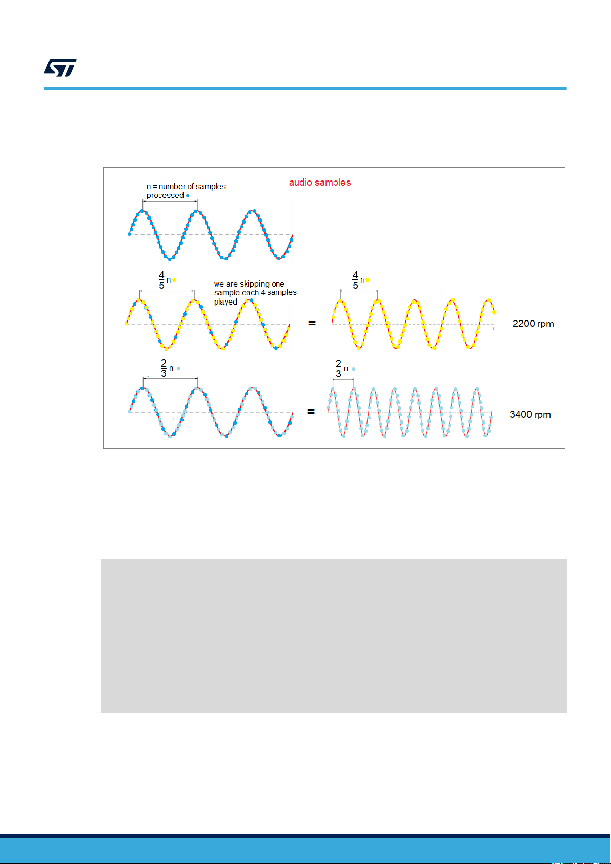
The acceleration and deceleration phases are simulated by increasing and decreasing the number of samples
reproduced. For example, consider that for an engine idling in Neutral at 800rpm, its sound may be represented
by a sinusoidal wave with period T. We simulate the acceleration phase by decreasing the period (increasing
signal frequency), as shown in the following figure.
Figure 44. Audio sample frequency modulation
UM2719 - Rev 3
page 52/60
Page 53
UM2719
Available demos for AEK-AUD-D903V1
The samples in the MCU memory are sampled at 44,100 Hz frequency, and frequency modulation is simulated by
varying the number of samples to be played. The following image shows the algorithm operating principle.
Figure 45. Varying sample numbers to simulate frequency modulation
The userFunction() used in this application has the following characteristics:
1. As soon as the application is started and the ignition command is given, the initial pointer is assigned to the
first sample to be played, while the final address is assigned to the last sample.
2. At the end of the first cycle (i.e., when the pointer to the current sample is the same as the pointer of the last
sample in the audio file for the first time), the algorithm no longer restarts from the first sample, but 90,000
samples after the first. This effectively simulates the effect of engine start and engine idle with a few seconds
of recording.
uint32_t userFunction()
{
if(acc_first_time)
{
wavfilePtr = wavfileBeginPtr = getStartWavFile(0);
wavfileEndPtr = getEndWavFile(0);
acc_first_time = false;
}
if(wavfilePtr > wavfileEndPtr)
wavfilePtr = wavfileBeginPtr + 90000;
int32_t amplitude = 0;
uint16_t sampleWav;
sampleWav = ( *wavfilePtr << 8) | ((*wavfilePtr >> 8) & 0xFF);
//raw sample, change endianness
amplitude = (int32_t)sampleWav;
The acceleration and deceleration is obtained through voltage variation from a potentiometer. This external input
is converted by the microcontroller SARADC, and its value is stored in an rpm variable. The higher the value of
rpm, the greater the number of samples to be skipped.
This method, shown in the code snippet below, can therefore simulate variations in engine rpm sounds in
acceleration and deceleration.
UM2719 - Rev 3
page 53/60
Page 54

if (rpm1 <= 2200)
{
if (rpm1 == 900)
{
if (j < 23)
wavfilePtr++;
else
{
wavfilePtr+ = 2;
j = 0;
}
}
else if (rpm1 == 1000)
{
if (j < 20)
wavfilePtr++
else
{
wavfilePtr+ = 2;
j = 0;
}
}
etc...
…
…
…
else if (rpm1 == 2200)
{
if (j < 12)
{
wavfilePtr++;
}
else
{
wavfilePtr =+ 4;
j = 0;
}
}
else//800 rpm
wavfilePtr++;
UM2719
Available demos for AEK-AUD-D903V1
UM2719 - Rev 3
page 54/60
Page 55

Revision history
Date Version Changes
19-May-2020 1 Initial release.
17-Feb-2021 2
15-Apr-2021 3
UM2719
T
able 11. Document revision history
Added Section 4 AEK-AUD-C1D9031 - single board AVAS solution, Section 4.1 Hardware overview,
Section 4.2 Software overview and Section 4.3 FCC and IC disclaimer
Updated Section 1 A
automotive power amplifier, Section 3.2 FDA903D I²S protocol Section 3.3 FDA903D I²C protocol,
Section 3.3.1 I²C protocol writing procedure and Section 3.6 Stereo mode.
VAS system hardware, Section 3 AEK-AUD-D903V1 evaluation board for
.
UM2719 - Rev 3
page 55/60
Page 56

Contents
UM2719
Contents
1 A
VAS system hardware ............................................................2
2 AEK-MCU-C1MLIT1 Discovery board audio support ................................3
2.1 I²S bus interface on the SPC582B60E1 microcontroller...............................4
2.1.1 I²S protocol details .......................................................4
2.1.2 I²S emulation on DSPI for SPC5 MCU control of FDA903D amplifier .................4
2.2 I²C bus interface on the SPC582B60E1 microcontroller ..............................6
3 AEK-AUD-D903V1 evaluation board for automotive power amplifier ................8
3.1 FDA903D finite state machine ....................................................8
3.1.1 FDA903D FSM state descriptions ...........................................10
3.2 FDA903D I²S protocol..........................................................10
3.3 FDA903D I²C protocol .........................................................11
3.3.1 I²C protocol writing procedure ..............................................12
3.3.2 I²C protocol: reading procedure.............................................14
3.3.3 IB registers in I²C .......................................................15
3.3.4 DB registers in I²C.......................................................16
3.3.5 Driver ................................................................17
3.4 Potentiometers ...............................................................17
3.5 Successive approximation analog-to-digital converter (SARADC) .....................18
3.6 Stereo mode .................................................................18
4 AEK-AUD-C1D9031 - single board AVAS solution..................................21
4.1 Hardware overview ............................................................21
4.2 Software overview.............................................................22
4.3 FCC and IC disclaimer .........................................................22
5 AVAS system software............................................................23
5.1 SPC5-STUDIO ...............................................................23
5.2 STSW-AUTODEVKIT ..........................................................23
5.3 AEK-AUD-D903V1.c and sound.c drivers .........................................23
5.3.1 AEK-AUD-D903V1.c driver ................................................23
5.3.2 sound.c description ......................................................28
6 How to play an audio WAV file ....................................................30
UM2719 - Rev 3
page 56/60
Page 57

UM2719
Contents
6.1 SPC582B60E1 memory map....................................................30
6.2 Uploading audio W
AV file ......................................................30
7 AEK-AUD-D903V1 sample applications............................................43
7.1 How to create a simple AEK-AUD-D903V1 application ..............................43
7.2 Available demos for AEK-AUD-D903V1...........................................49
7.2.1 How to upload the demos for AEK-AUD-D903V1 ...............................49
7.2.2 Mono audio – Test Application (SPC584Bxx and SPC58ECxx).....................51
7.2.3 I²C Software Mono audio – Test Application (SPC582Bxx and SPC58ECxx) ..........51
7.2.4 Mono audio and Diagnostic - Test Application (SPC582Bxx).......................51
7.2.5 Stereo audio and Diagnostic - Test Application (SPC582Bxx) ......................52
7.2.6 Engine Sound Simulator - Test Application for AVAS purpose (SPC582Bxx)...........52
Revision history .......................................................................55
UM2719 - Rev 3
page 57/60
Page 58

List of figures
UM2719
List of figures
Figure 1. A
Figure 2. AVAS demo hardware and connections ...................................................2
Figure 3. AEK-MCU-C1MLIT1 Discovery board components ...........................................3
Figure 4. Standard I²S data format .............................................................5
Figure 5. Connector CN10 pins for DSPI0 ........................................................5
Figure 6. I²C typical data format ............................................................... 6
Figure 7. Connector CN10 pins dedicated to I²C .................................................... 7
Figure 8. AEK-AUD-D903V1 main components and interfaces ..........................................8
Figure 9. FDA903D state machine ............................................................. 9
Figure 10. I²S (DSPI) connection in AEK-AUD-D903V1 ............................................... 11
Figure 11. I²C connection in AEK-AUD-D903V1 ....................................................12
Figure 12. ENABLE pin locations on the connector .................................................. 13
Figure 13. Read operation packet.............................................................. 14
Figure 14. Read operation required data .........................................................14
Figure 15. Read operation with repeated start condition .............................................. 14
Figure 16. Linear potentiometer circuit .......................................................... 17
Figure 17. Potentiometer connections ........................................................... 18
Figure 18. AVAS system for two stereo sound ..................................................... 19
Figure 19. AEK-MCU-C1MLIT1 seen on both sides ................................................. 20
Figure 20. AEK-AUD-C1D9031 components ......................................................21
Figure 21. API AEK_903D_Play(AEK_AUD_D903V0)................................................ 25
Figure 22. I2S Test Pin configuration API ........................................................ 25
Figure 23. playSound API ................................................................... 29
Figure 24. Project folder for audio files .......................................................... 31
Figure 25. Old flash block memory allocation ...................................................... 32
Figure 26. New flash block memory allocation .....................................................32
Figure 27. sounddb definition................................................................. 33
Figure 28. sounddb.s audio file declarations ...................................................... 34
Figure 29. Build output before adding sounddb.s component ........................................... 35
Figure 30. Build output after adding sounddb.s component ............................................ 35
Figure 31. Open hex file with editor ............................................................ 36
Figure 32. hex file data ..................................................................... 37
Figure 33. Starting point of audio content in hex file ................................................. 38
Figure 34. sounddb.s file with audio sample file paths removed ......................................... 39
Figure 35. SPC5-UDESTK-SW software with loader window ........................................... 40
Figure 36. FLASH/OTP Memory Programming Tool ................................................. 41
Figure 37. UDE Flash erase tool .............................................................. 41
Figure 38. SPC5-STUDIO adding audio project components ........................................... 43
Figure 39. AEK-AUD-D903V1 component configuration .............................................. 44
Figure 40. AEK-AUD-D903V1 I²C configuration ....................................................45
Figure 41. PinMap editor .................................................................... 46
Figure 42. SPC5-STUDIO Import application Wizard ................................................ 50
Figure 43. SPC5-STUDIO application library ...................................................... 51
Figure 44. Audio sample frequency modulation .................................................... 52
Figure 45. Varying sample numbers to simulate frequency modulation .................................... 53
VAS system AutoDevKit control board and audio board .......................................1
UM2719 - Rev 3
page 58/60
Page 59

UM2719
List of tables
List of tables
T
able 1. I²C device address combinations .........................................................9
Table 2. Legacy mode Enable configurations ......................................................10
Table 3. I²C address 1 selection ...............................................................12
Table 4. Subaddress association .............................................................. 13
Table 5. IB register map .................................................................... 15
Table 6. DB register map.................................................................... 16
Table 7. Comparison of pin settings for addresses 1 and 3 ............................................ 20
Table 8. FDA903D IB8 register description ....................................................... 24
Table 9. list of API functions in AEK-AUD-D903V1.c ................................................. 26
Table 10. Flash memory map of SPC582B ........................................................ 30
Table 11. Document revision history ............................................................. 55
UM2719 - Rev 3
page 59/60
Page 60

UM2719
IMPORTANT NOTICE – PLEASE READ CAREFULLY
STMicroelectronics NV and its subsidiaries (“ST”) reserve the right to make changes, corrections, enhancements, modifications, and improvements to ST
products and/or to this document at any time without notice. Purchasers should obtain the latest relevant information on ST products before placing orders. ST
products are sold pursuant to ST’
Purchasers are solely responsible for the choice, selection, and use of ST products and ST assumes no liability for application assistance or the design of
Purchasers’ products.
No license, express or implied, to any intellectual property right is granted by ST herein.
Resale of ST products with provisions different from the information set forth herein shall void any warranty granted by ST for such product.
ST and the ST logo are trademarks of ST. For additional information about ST trademarks, please refer to www
names are the property of their respective owners.
Information in this document supersedes and replaces information previously supplied in any prior versions of this document.
s terms and conditions of sale in place at the time of order acknowledgement.
.st.com/trademarks. All other product or service
© 2021 STMicroelectronics – All rights reserved
UM2719 - Rev 3
page 60/60
 Loading...