

Page 1

AN5326
Application note
AIS2DW12: ultra-low-power 3-axis accelerometer for automotive applications
Introduction
This document is intended to provide usage information and application hints related to ST’s AIS2DW12 motion sensor.
The AIS2DW12 is an ultra-low-power three-axis linear accelerometer designed to address nonsafety automotive applications
which leverages on the robust and mature manufacturing processes already used for the production of micromachined
accelerometers.
The device has four different ultra-low-power modes, two user-selectable full scales (±2g/±4g) and is capable of measuring
accelerations with output data rates from 1.6 Hz to 100 Hz.
The AIS2DW12 has an integrated 32-level first-in, first-out (FIFO) buffer allowing the user to store data in order to limit
intervention by the host processor. The device includes a dedicated internal engine to process motion and acceleration
detection including free-fall, motion and no-motion, wakeup, activity/inactivity and 6D/4D orientation.
The embedded self-test capability allows the user to check the functioning of the sensor in the final application.
The AIS2DW12 is available in a small thin plastic land grid array package (LGA) and it is guaranteed to operate over an
extended temperature range from -40 °C to +85 °C.
AN5326 - Rev 3 - January 2021
For further information contact your local STMicroelectronics sales office.
www.st.com
Page 2

1 Pin description
1
9
8
7
2
3
46 5
11 12
10
GND
RES
SCL/SPC
CS
SDO/SA0
SDA/SDI/SDO
NC
INT2
INT1
(TOPVIEW)
DIRECTION OF THE
DETECTABLE
ACCELERATIONS
Y
1
X
Z
VDD
(BOTTOM VIEW)
GND
VDDIO
AN5326
Pin description
Figure 1. Pin connections
Table 1. Pin description
Pin# Name Function Pin status
SCL
1
2 CS
3
4
5 NC Internally not connected. Can be tied to VDD, VDDIO, or GND.
6 GND 0 V supply
7 RES Connect to GND
8 GND 0 V supply
9 VDD Power supply
10 VDD_IO Power supply for I/O pins
11 INT2 Interrupt pin 2. Clock input when selected in single data conversion on demand. Default: push-pull output forced to ground
12 INT1 Interrupt pin 1 Default: push-pull output forced to ground
1. In order to disable the internal pull-up on the CS pin, write '1' to the CS_PU_DISC bit in CTRL2 (21h).
2. Internal pull-up on SDO/SA0 pin cannot be disabled. Do not connect this pin to GND in low-power
applications.
I²C serial clock (SCL)
SPC
SPI serial port clock (SPC)
SPI enable
I²C/SPI mode selection
(1: SPI idle mode / I²C communication enabled;
0: SPI communication mode / I²C disabled)
SDO
SPI serial data output (SDO)
SA0
I²C less significant bit of the device address (SA0)
SDA
I²C serial data (SDA)
SDI
SPI serial data input (SDI)
SDO
3-wire interface serial data output (SDO)
Default: input without internal pull-up
Default: input with internal pull-up
Default: input with internal pull-up
Default: (SDA) input without internal pull-up
(1)
(2)
AN5326 - Rev 3
page 2/42
Page 3

AN5326 - Rev 3
page 3/42
2 Registers
Table 2. Registers
Register name Address Bit7 Bit6 Bit5 Bit4 Bit3 Bit2 Bit1 Bit0
OUT_T_L 0Dh TEMP3 TEMP2 TEMP1 TEMP0 0 0 0 0
OUT_T_H
WHO_AM_I
(1)
(1)
CTRL1 20h ODR3 ODR2 ODR1 ODR0 OP_MODE1 OP_MODE0 PW_MODE1 PW_MODE0
CTRL2 21h BOOT SOFT_RESET 0 CS_PU_DISC BDU IF_ADD_INC I2C_DISABLE SIM
CTRL3 22h ST2 ST1 PP_OD LIR H_LACTIVE 0
CTRL4_INT1 23h INT1_6D 0 INT1_WU INT1_FF 0 INT1_DIFF5 INT1_FTH INT1_DRDY
CTRL5_INT2 24h
CTRL6 25h BW_FILT1 BW_FILT0 FS1 FS0 FDS 0 0 0
(1)
OUT_T
(1)
STATUS
OUT_X_L
OUT_X_H
OUT_Y_L
OUT_Y_H
OUT_Z_L
OUT_Z_H
(1)
(1)
(1)
(1)
(1)
(1)
FIFO_CTRL 2Eh FMode2 FMode1 FMode0 FTH4 FTH3 FTH2 FTH1 FTH0
FIFO_SAMPLES
(1)
SIXD_THS 30h 4D_EN 6D_THS1 6D_THS0 0 0 0 0 0
WAKE_UP_THS 34h 0 SLEEP_ON WK_THS5 WK_THS4 WK_THS3 WK_THS 2 WK_THS 1 WK_THS 0
WAKE_UP_DUR 35h FF_DUR5 WAKE_DUR1 WAKE_DUR0 STATIONARY SLEEP_DUR3 SLEEP_DUR2 SLEEP_DUR1 SLEEP_DUR0
FREE_FALL 36h FF_DUR4 FF_DUR3 FF_DUR2 FF_DUR1 FF_DUR0 FF_THS2 FF_THS1 FF_THS0
STATUS_DUP
WAKE_UP_SRC
(1)
(1)
0Eh TEMP11 TEMP10 TEMP9 TEMP8 TEMP7 TEMP6 TEMP5 TEMP4
0Fh 0 1 0 0 0 1 0 0
INT2_
SLEEP_
STATE
INT2_
SLEEP_CHG
INT2_BOOT
INT2_
DRDY_T
SLP_MODE
_SEL
INT2_OVR INT2_DIFF5 INT2_FTH INT2_DRDY
SLP_MODE_1
26h TEMP7 TEMP6 TEMP5 TEMP4 TEMP3 TEMP2 TEMP1 TEMP0
27h FIFO_THS WU_IA SLEEP_STATE 0 0 6D_IA FF_IA DRDY
28h X_L7 X_L6 X_L5 X_L4
X_L3
(2)
X_L2
(2)
0 0
29h X_H7 X_H6 X_H5 X_H4 X_H3 X_H2 X_H1 X_H0
2Ah Y_L7 Y_L6 Y_L5 Y_L4
Y_L3
(2)
Y_L2
(2)
0 0
2Bh Y_H7 Y_H6 Y_H5 Y_H4 Y_H3 Y_H2 Y_H1 Y_H0
2Ch Z_L7 Z_L6 Z_L5 Z_L4
Z_L3
(2)
Z_L2
(2)
0 0
2Dh Z_H7 Z_H6 Z_H5 Z_H4 Z_H3 Z_H2 Z_H1 Z_H0
2Fh FIFO_FTH FIFO_OVR Diff5 Diff4 Diff3 Diff2 Diff1 Diff0
37h OVR DRDY_T SLEEP_STATE_IA 0 0 6D_IA FF_IA DRDY
38h 0 0 FF_IA SLEEP_STATE IA WU_IA X_WU Y_WU Z_WU
AN5326
Registers
Page 4

AN5326 - Rev 3
Register name Address Bit7 Bit6 Bit5 Bit4 Bit3 Bit2 Bit1 Bit0
SIXD_SRC
ALL_INT_SRC
X_OFS_USR 3Ch X_OFS_USR_7 X_OFS_USR_6 X_OFS_USR_5 X_OFS_USR_4 X_OFS_USR_3 X_OFS_USR_2 X_OFS_USR_1 X_OFS_USR_0
Y_OFS_USR 3Dh Y_OFS_USR_7 Y_OFS_USR_6 Y_OFS_USR_5 Y_OFS_USR_4 Y_OFS_USR_3 Y_OFS_USR_2 Y_OFS_USR_1 Y_OFS_USR_0
Z_OFS_USR 3Eh Z_OFS_USR_7 Z_OFS_USR_6 Z_OFS_USR_5 Z_OFS_USR_4 Z_OFS_USR_3 Z_OFS_USR_2 Z_OFS_USR_1 Z_OFS_USR_0
(1)
(1)
CTRL7 3Fh
3Ah 0 6D_IA ZH ZL YH YL XH XL
3Bh 0 0
DRDY_
PULSED
INT2_ON_INT1
SLEEP_
CHANGE_IA
INTERRUPTS
_ENABLE
6D_IA 0 0 WU_IA FF_IA
USR_OFF_ON
_OUT
USR_OFF_ON
_WU
USR_OFF_W
HP_REF_
MODE
1. Read-only register
2. If Low-Power Mode 1 is enabled, this bit is set to 0.
LPASS_ON6D
page 4/42
AN5326
Registers
Page 5

3 Operating modes
3.1 Power mode
Four sets of operating modes have been designed to offer the customer a broad choice of noise/powerconsumption combinations.
Power Mode 4 Power Mode 3 Power Mode 2 Power Mode 1
14-bit 14-bit 14-bit 12-bit
These operating modes are selected by writing the OP_ MODE[1:0] and PW_MODE[1:0] bits in CTRL1 (20h)
given in the tables below. Additional details concerning power consumption and noise in different operating
modes are available in the device datasheet.
AN5326
Operating modes
Table 3. Accelerometer resolution
Table 4. CTRL1 register
b7 b6 b5 b4 b3 b2 b1 b0
ODR3 ODR2 ODR1 ODR0 OP_MODE1 OP_MODE0 PW_MODE1 PW_MODE0
Table 5. Operating mode selection
OP_MODE[1:0] Operating mode and resolution
00 Continuous mode (12/14-bit resolution)
01 Not allowed
10 Single data conversion on-demand mode (12/14-bit resolution)
11 Not allowed
Table 6. Power mode selection
PW_MODE[1:0]
00 Power Mode 1 (12-bit resolution)
01 Power Mode 2 (14-bit resolution)
10 Power Mode 3 (14-bit resolution)
11 Power Mode 4 (14-bit resolution)
Power mode and resolution
AN5326 - Rev 3
page 5/42
Page 6

3.2 Continuous conversion
When bits OP_MODE[1:0] in CTRL1 (20h) are set to Continuous Mode (00b), the device is in continuous
conversion and the output data rate can be selected through the ODR[3:0] bits in CTRL1 (20h).
ODR[3:0] Output data rate
0000 Power-down
0001 1.6 Hz (independent of power mode)
0010 12.5 Hz (independent of power mode)
0011 25 Hz (independent of power mode)
0100 50 Hz (independent of power mode)
0101 100 Hz (independent of power mode)
AN5326
Continuous conversion
Table 7. Output data rate selection
AN5326 - Rev 3
page 6/42
Page 7
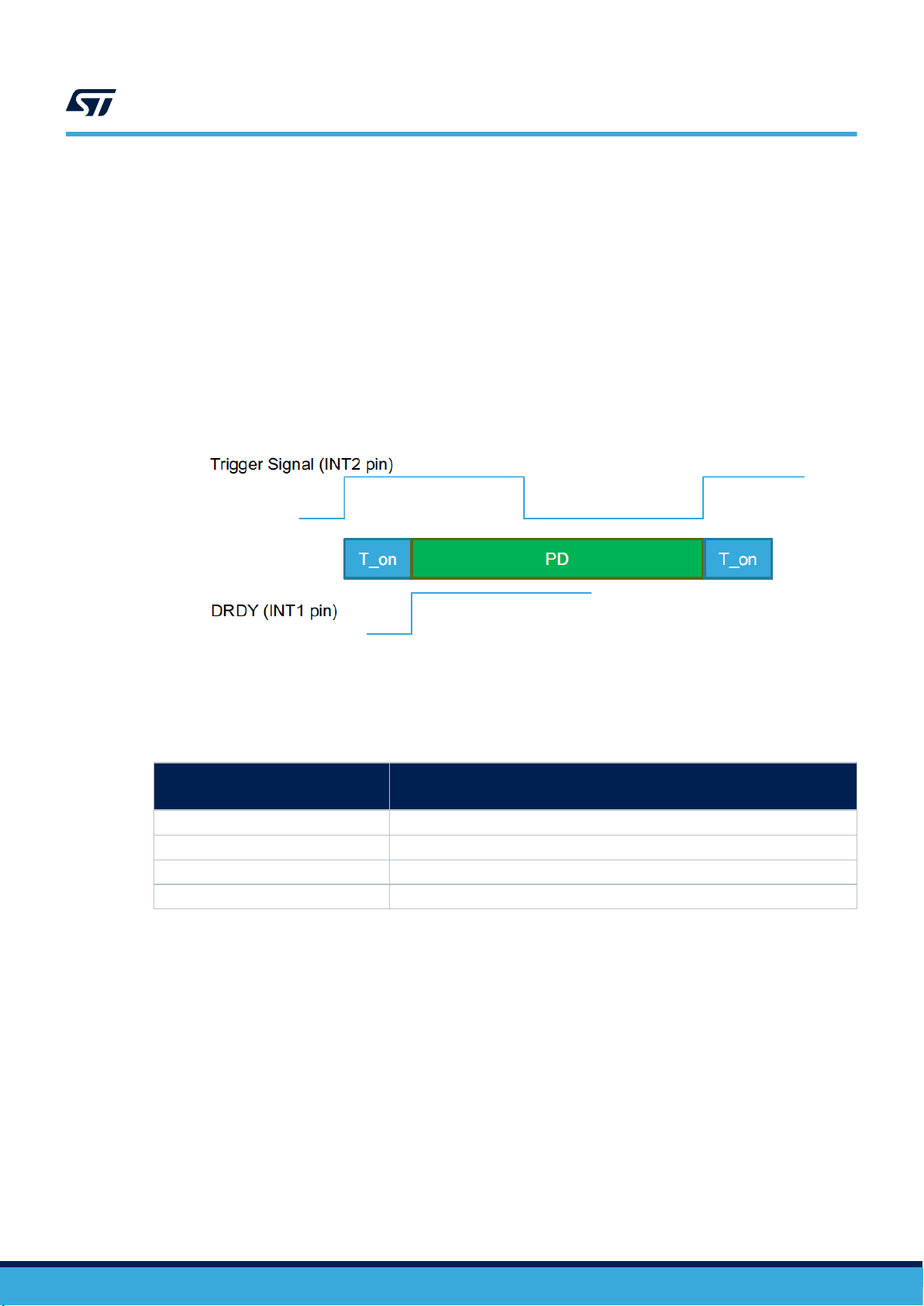
3.3 Single data conversion (on-demand mode)
This mode is enabled by writing the OP_MODE[1:0] bits to ‘10' in CTRL1 (20h).
In this configuration the device waits for a trigger signal in order to generate new data according to the selected
power mode PW_MODE[1:0] bits in CTRL1 (20h), after that the device immediately enters power-down.
The trigger can be:
• A rising edge on the INT2 pin (if SLP_MODE_SEL = ‘0' in register CTRL3 (22h)). In this case the user
can detect the end of the conversion using the DRDY bit of the STATUS register (27h) that can also be
routed to the INT1 pin by setting the INT1_DRDY bit to 1 in register CTRL4_INT1 (23h). Minimum duration
of trigger signal high level is 20 ns.
• A write of SLP_MODE_1 to ‘1' in register CTRL3 (22h) (if SLP_MODE_SEL ='1' in register CTRL3
(22h)). In this case, the user can detect the end of the conversion using the DRDY bit/signal as in the
previous case, or by checking when the SLP_MODE_1 bit in register CTRL3 (22h) is automatically cleared.
Figure 2. Single data conversion using INT2 as external trigger (SLP_MODE_SEL = 0)
AN5326
Single data conversion (on-demand mode)
The maximum data rate using single data conversion mode is 100 Hz and the time of conversion depends on the
low-power mode selected (refer to the following table).
Table 8. Single data conversion: typical time of conversion
Power mode
Mode 1 1.20 ms
Mode 2 1.70 ms
Mode 3 2.30 ms
Mode 4 3.55 ms
Typical time of conversion
(T_on)
Note: If the ODR[3:0] bits of the CTRL1 register are set to 0000b, the accelerometer is permanently configured in
Power-down mode and no conversion can be triggered. When the single data conversion mode has to be used,
the ODR[3:0] bits of the CTRL1 register must be different than 0000b.
Interrupts, embedded features and FIFO are still supported when using single data conversion mode. Also the
embedded filters LPF1, LPF2 and HP are available in single data conversion (on-demand mode) with the same
bandwidth and settling time of the selected low-power mode (see Section 3.4 Accelerometer bandwidth for
details).
AN5326 - Rev 3
page 7/42
Page 8
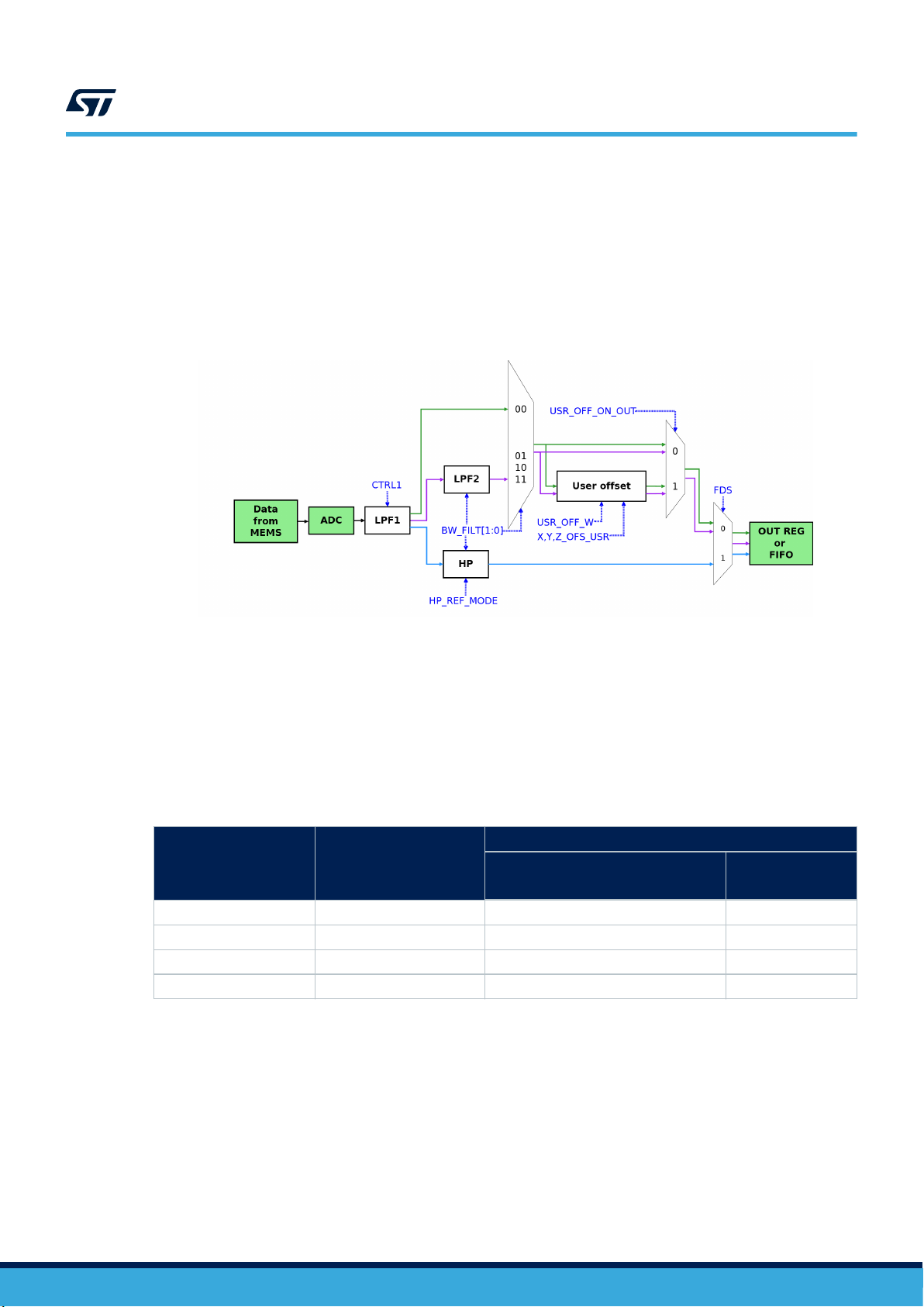
3.4 Accelerometer bandwidth
The accelerometer sampling chain (Figure 3. Accelerometer filtering chain diagram) is represented by a cascade
of a few blocks:
• ADC: Analog-to-digital converter
• LPF1(2): low-pass filter 1(2)
• HP: high-pass filter
• User offset: configurable values that are subtracted from the sampled data (one for each axis)
Figure 3. Accelerometer filtering chain diagram
AN5326
Accelerometer bandwidth
As shown in the figure above, data can be generated using three different filter paths:
• only LPF1 (green path) : in order to select this path set BW_FILT[1:0] = 00 and FDS = 0. Additional details in
Table 9. Low-pass filter 1 bandwidth.
• LPF1 + LPF2 (purple path) : in order to select this path set BW_FILT[1:0] to a value different from 00 and
FDS = 0. Additional details in Table 10. Bandwidth: low-pass path.
• LPF1 + HP (blue path): these outputs are available by setting FDS = 1. Additional details in
Table 11. Bandwidth: high-pass path.
Table 9. Low-pass filter 1 bandwidth
BW_FILT[1:0] = 00
Mode
Power Mode 4 @ each ODR
Power Mode 3 @ each ODR 0 360
Power Mode 2 @ each ODR 0 720
Power Mode 1 @ each ODR 0 3200
1. The starting condition of ODR[3:0],OP_ MODE[1:0], PW_MODE[1:0] and BW_FILT[1:0] do not impact these values. The
turn-on time (first sample available starting from power-down condition) is 1 / ODR.
ODR selection
Samples to discard
Settling @95%
0 180
(1)
Cutoff [Hz]
AN5326 - Rev 3
page 8/42
Page 9

AN5326
Accelerometer bandwidth
Table 10. Bandwidth: low-pass path
BW_FILT[1:0] = 01 BW_FILT[1:0] = 10 BW_FILT[1:0] = 11
Mode ODR selection
PW Mode 4 @ each ODR
Samples to
discard
(1)
Settling @95%
Cutoff [Hz]
Samples to discard
Settling @95%
1 ODR/4 5 ODR/10 11 ODR/20
PW Mode 3 @ each ODR 1 ODR/4 5 ODR/10 11 ODR/20
PW Mode 2 @ each ODR 1 ODR/4 5 ODR/10 11 ODR/20
PW Mode 1 @ each ODR 1 ODR/4 5 ODR/10 11 ODR/20
1. The starting condition of ODR[3:0], OP_MODE[1:0], PW_MODE[1:0] and BW_FILT[1:0] do not impact these
values.
Table 11. Bandwidth: high-pass path
BW_FILT[1:0] = 01 / 00 BW_FILT[1:0] = 10 BW_FILT[1:0] = 11
Mode ODR selection
PW Mode 4 @ each ODR
PW Mode 3 @ each ODR 1 ODR/4 5 ODR/10 11 ODR/20
PW Mode 2 @ each ODR 1 ODR/4 5 ODR/10 11 ODR/20
PW Mode 1 @ each ODR 1 ODR/4 5 ODR/10 11 ODR/20
Samples to
discard
(1)
Settling @95%
Cutoff [Hz]
Samples to discard
Settling @95%
1 ODR/4 5 ODR/10 11 ODR/20
(1)
Cutoff
[Hz]
(1)
Cutoff
[Hz]
Samples to discard
Settling @95%
Samples to discard
Settling @95%
(1)
Cutoff
[Hz]
(1)
Cutoff
[Hz]
1. The starting condition of ODR[3:0], OP_MODE[1:0], PW_MODE[1:0] and BW_FILT[1:0] do not impact these
values.
Setting USR_OFF_ON_OUT = 1 in CTRL7 does not change the bandwidth of the system. In this configuration,
the values written in registers X_OFS_USR, Y_OFS_USR, Z_OFS_USR are subtracted from the respective axis.
The offset values are signed values (two's complement).
The weight of the bits in registers X_OFS_USR, Y_OFS_USR, Z_OFS_USR is defined through the USR_OFF_W
bit in CTRL7.
AN5326 - Rev 3
page 9/42
Page 10
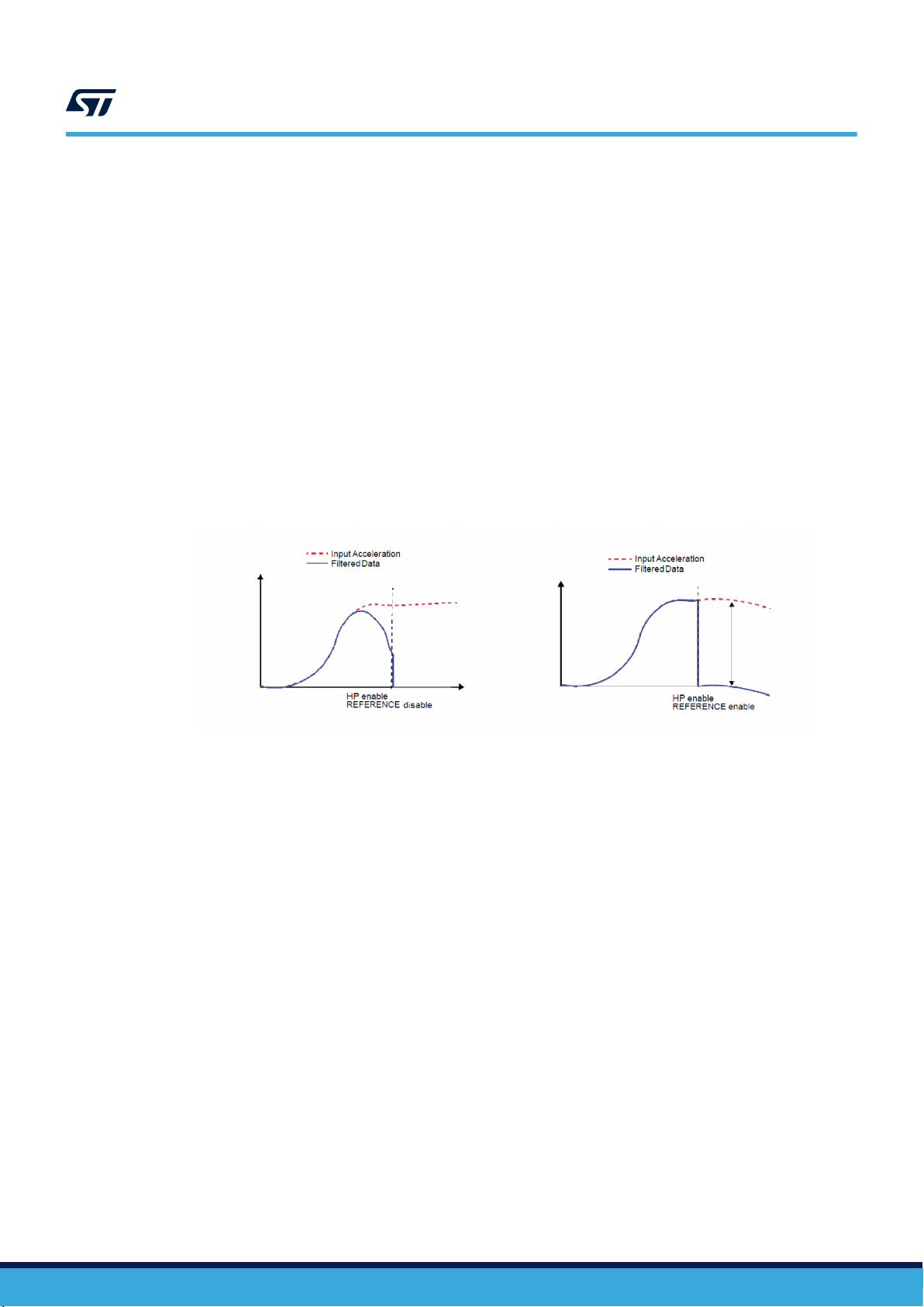
3.5 High-pass filter configuration
The AIS2DW12 provides an embedded high-pass filtering capability to easily delete the DC component of the
measured acceleration. As shown in Figure 3. Accelerometer filtering chain diagram, through the FDS bit in
register CTRL6 the user can route the filter outputs to the output registers.
It is also possible to independently apply the filter to the embedded function data (Figure 6. Embedded functions
in Section 5 Interrupt generation and embedded functions). This means that it is possible to get filtered data
while the interrupt generation works on unfiltered data.
The high-pass filter can be configured in reference mode by setting the HP_REF_MODE bit in the CTRL7 register
to 1. In this configuration the output data is calculated as the difference between the measured acceleration and
the output values captured when reference mode was enabled. In this way only the difference is applied without
any filtering.
As an example, this feature can be combined with the wake-up functionality described in Section 5.4 in order
to detect when the device is displaced with respect to a specific orientation, i.e. the orientation of the device
when the HP_REF_MODE bit was set to 1. When the output acceleration exceeds the wake-up threshold defined
by the WK_THS[5:0] bits in the WAKE_UP_THS register for a duration longer than the one defined by the
WAKE_DUR[1:0] bits in the WAKE_UP_DUR register, an interrupt is generated. If the device is moved back to the
original reference orientation, the interrupt is deactivated.
Figure 4. High-pass filter in normal and reference mode
AN5326
High-pass filter configuration
AN5326 - Rev 3
page 10/42
Page 11

4 Reading output data
4.1 Startup sequence
Once the device is powered up, it automatically downloads the calibration coefficients from the embedded
non-volatile memory to the internal registers. When the boot procedure is completed, i.e. after approximately
20 milliseconds, the accelerometer automatically enters power-down. The default status of the pins with both VDD
and VDDIO "on" is indicated in Table 1. Pin description.
Note: VDD cannot be lower than VDDIO. VDD = 0 V and VDDIO "on" is allowed: when this power supply
configuration is applied, an internal pull-up is applied also to the SDA and SCL pins (the other pins maintain the
default status indicated in Table 1).
To turn on the accelerometer and gather acceleration data, it is necessary to select one of the operating modes
through the CTRL1 register.
Refer to Section 3 Operating modes for a detailed description of data generation.
4.2 Using the status register
The device is provided with a STATUS register which can be polled to check when a new set of data is available.
The DRDY bit is set to 1 when a new set of data is available from the accelerometer output.
The read operations should be performed as follows:
1. Read STATUS
2. If DRDY = 0, then go to 1
3. Read OUT_X_L
4. Read OUT_X_H
5. Read OUT_Y_L
6. Read OUT_Y_H
7. Read OUT_Z_L
8. Read OUT_Z_H
9. Data processing
10. Go to 1
AN5326
Reading output data
4.3 Using the data-ready signal
The device can be configured to have one hardware signal to determine when a new set of measurement data is
available to be read.
The data-ready signal is derived from the DRDY bit of the STATUS register. The signal can be driven to the INT1
pin by setting the INT1_DRDY bit of the CTRL4_INT1 register to 1 and to the INT2 pin by setting the INT2_DRDY
bit of the CTRL5_INT2 register to 1.
The data-ready signal rises to 1 when a new set of data has been measured and is available to be read. In
DRDY latched mode (DRDY_PULSED bit = 0 in CTRL7 register), which is the default condition, the signal gets
reset when the higher part of one of the channels has been read (29h, 2Bh, 2Dh). In DRDY pulsed mode
(DRDY_PULSED = 1) the pulse duration can vary between 105 μs and 175 μs. Pulsed mode is not applied to the
DRDY bit which is always latched.
AN5326 - Rev 3
page 11/42
Page 12
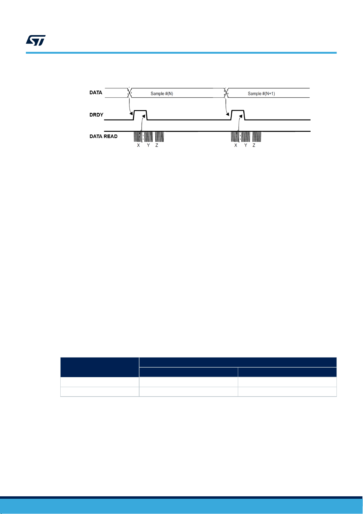
Figure 5. Data-ready signal
4.4 Using the block data update (BDU) feature
If reading the accelerometer data is particularly slow and cannot be synchronized (or it is not required) with either
the DRDY event bit in the STATUS register or with the DRDY signal driven to the INT1/INT2 pins, it is strongly
recommended to set the BDU (block data update) bit to 1 in the CTRL2 (21h) register.
This feature avoids reading values (most significant and least significant parts of output data) related to different
samples. In particular, when the BDU is activated, the data registers related to each channel always contain
the most recent output data produced by the device, but, in case the read of a given pair (i.e. OUT_X_H and
OUT_X_L, OUT_Y_H and OUT_Y_L, OUT_Z_H and OUT_Z_L) is initiated, the refresh for that pair is blocked
until both MSB and LSB parts of the data are read.
Note: BDU only guarantees that the LSB part and MSB part of one data channel have been sampled at the same
moment. For example, if the reading speed is too slow, X and Y can be read at T1 and Z sampled at T2.
AN5326
Using the block data update (BDU) feature
4.5 Understanding output data
The measured acceleration data are sent to the OUT_X_H, OUT_X_L, OUT_Y_H, OUT_Y_L, OUT_Z_H, and
OUT_Z_L registers. These registers contain, respectively, the most significant part and the least significant part of
the acceleration signals acting on the X, Y, and Z axes.
The complete output data for the X, Y, Z channels is given by the concatenation OUT_X_H & OUT_X_L,
OUT_Y_H & OUT_Y_L , OUT_Z_H & OUT_Z_L.
Acceleration data is represented as 16-bit numbers, left-aligned and encoded in two’s complement. These values
(LSB) have different resolution according to the selected operating mode.
After calculating the LSB, it must be multiplied by the proper sensitivity parameter to obtain the corresponding
value in mg.
Full Scale
±2 g
±4 g 1.952 0.488
Table 12. Sensitivity
Sensitivity [mg/LSB]
12-bit format 14-bit format
0.976 0.244
AN5326 - Rev 3
page 12/42
Page 13

4.5.1 Example of output data
Below is a simple example of how to use the LSB data and transform it into mg.
The values are given under the hypothesis of ideal device calibration (i.e., no offset, no gain error, etc.).
Get raw data from the sensor in 14-bit power mode at ±2 g:
OUT_X_L: 60h
OUT_X_H: FDh
OUT_Y_L: 78h
OUT_Y_H: 00h
OUT_Z_L: FCh
OUT_Z_H: 42h
Do register concatenation:
AN5326
Understanding output data
OUT_X_H & OUT_X_L: FD60h
OUT_Y_H & OUT_Y_L: 0078h
OUT_Z_H & OUT_Z_L: 42FCh
Apply sensitivity (e.g., 14-bit resolution, 0.244 at full scale ±2 g):
X: -672 / 4 * 0.244 = -41 mg
Y: +120 / 4 * 0.244 = +7 mg
Z: +17148 / 4 * 0.244 = +1046 mg
AN5326 - Rev 3
page 13/42
Page 14

Interrupt generation and embedded functions
5 Interrupt generation and embedded functions
Figure 6. Embedded functions
AN5326
In order to generate an interrupt, the AIS2DW12 device has to be set in an active operating mode (not in
power-down) because generation of the interrupt is based on accelerometer data.
The interrupt generator can be configured to detect:
• Free-fall;
• Wake-up;
• 6D/4D orientation detection;
• Activity/Inactivity detection.
All these interrupt signals, together with the FIFO interrupt signals and sensor data-ready, can be driven to the
INT1 and/or INT2 interrupt pins or checked by reading the dedicated source register bits.
The H_LACTIVE bit of the CTRL3 register must be used to select the polarity of the interrupt pins. If this bit
is set to 0 (default value), the interrupt pins are active high and they change from low to high level when the
related interrupt condition is verified. Otherwise, if the H_LACTIVE bit is set to 1 (active low), the interrupt pins are
normally at high level and they change from high to low when the interrupt condition is reached.
The PP_OD bit of CTRL3 allows changing the behavior of the interrupt pins also when the DRDY signal is routed
to them from push-pull to open drain. If the PP_OD bit is set to 0, the interrupt pins are in push-pull configuration
(low-impedance output for both high and low level). When the PP_OD bit is set to 1, only the interrupt active state
is a low-impedance output.
The LIR bit of CTRL3 allows applying the latched mode to the interrupt signals (not affecting the DRDY signal).
When the LIR bit is set to 1, once the interrupt pin is asserted, it must be reset by reading the related interrupt
source register. If the LIR bit is set to 0, the interrupt signal is automatically reset when the interrupt condition is
no longer verified or after a certain amount of time in function of the type of interrupt.
AN5326 - Rev 3
page 14/42
Page 15

Note: If latched mode is enabled (LIR = 1), it is not recommended to continuously poll the ALL_INT_SRC or the
dedicated source registers because by reading them the embedded functions are internally reset; a synchronous
(with interrupt event) read of the source registers is recommended in this case.
5.1 Interrupt pin configuration
The device is provided with two pins that can be activated to generate:
• device status signals (such as data-ready and boot);
• embedded function interrupt signals;
• notification FIFO signals.
All the embedded function interrupt signals are subordinate to the INTERRUPTS_ENABLE bit in register CTRL7.
If this bit is set, the embedded functions are enabled and the interrupt signals can be routed on the INT1 and/or
INT2 pins; otherwise, if this bit is not set, the embedded functions are disabled. The INT2 pin can also become an
input pin when it is used as an external trigger in single data conversion (on-demand) mode. In order to configure
the device in this mode the user must set bits OP_MODE[1:0] = 10 in register CTRL1 and bit SLP_MODE_SEL =
0 in register CTRL3. It is possible to route all the INT2 pin signals on the INT1 pin by setting bit INT2_ON_INT1 =
1 in register CTRL7.
AN5326
Interrupt pin configuration
Figure 7. Interrupt pin configuration
AN5326 - Rev 3
The description of the interrupt control registers appears below; the default value of their bits is equal to 0, which
corresponds to "disable". In order to enable the routing of a specific interrupt signal on the pin, the corresponding
bit has to be set to 1.
Table 13. CTRL4_INT1
b7
INT1_6D 0 INT1_WU INT1_FF 0 INT1_DIFF5 INT1_FTH INT1_DRDY
b6 b5 b4 b3 b2 b1 b0
• INT1_6D: 6D recognition is routed to the INT1 pin.
• INT1_WU: Wakeup event recognition is routed to the INT1 pin.
page 15/42
Page 16

• INT1_FF: Free-fall event recognition is routed to the INT1 pin.
• INT1_DIFF5: FIFO full recognition is routed to the INT1 pin.
• INT1_FTH: FIFO threshold event is routed to the INT1 pin.
• INT1_DRDY: Accelerometer data-ready is routed to the INT1 pin.
Table 14. CTRL5_INT2
b7 b6 b5 b4 b3 b2 b1 b0
INT2_
SLEEP_STATE
INT2_
SLEEP_CHG
INT2_BOOT INT2_DRDY_T INT2_ OVR INT2_DIFF5 INT2_FTH INT2_DRDY
• INT2_SLEEP_STATE: Enable routing of SLEEP_STATE to the INT2 pin.
• INT2_SLEEP_CHG: Sleep change status routed to the INT2 pin.
• INT2 _BOOT: Boot state routed to the INT2 pin.
• INT2_DRDY_T: Temperature data-ready is routed to the INT2 pin.
• INT2 _OVR: FIFO overrun interrupt is routed to the INT2 pin.
• INT2_DIFF5: FIFO full recognition is routed to the INT2 pin.
• INT2_FTH: FIFO threshold event is routed to the INT2 pin.
• INT2_DRDY: Accelerometer data-ready to the INT2 pin.
AN5326
Event status
5.2 Event status
If multiple interrupt signals are routed on the same pin (INTx), the logic level of this pin is the “OR” combination of
the selected interrupt signals. In order to know which event has generated the interrupt condition, the application
should read the proper status register, which also will clear the event.
As indicated below, the STATUS register is 'partially' duplicated at address 37h in order to allow a multiple read of
consecutive registers.
• STATUS (27h) or STATUS_DUP (37h);
• WAKE_UP_SRC (38h);
• SIXD_SRC (3Ah);
• ALL_INT_SRC (3Bh).
AN5326 - Rev 3
page 16/42
Page 17

5.3 Free-fall interrupt
Free-fall detection refers to a specific register configuration that allows recognizing when the device is in free-fall:
the acceleration measured along all the axes goes to zero. In a real case a “free-fall zone” is defined around the
zero-g level where all the accelerations are small enough to generate the interrupt. Configurable threshold and
duration parameters are associated to free-fall event detection: the threshold parameter defines the free-fall zone
amplitude; the duration parameter defines the minimum duration of the free-fall interrupt event to be recognized
(Figure 8. Free-fall interrupt).
AN5326
Free-fall interrupt
Figure 8. Free-fall interrupt
The free-fall event signal can be routed to the INT1 pin by setting the INT1_FF bit of the CTRL4_INT1 register to
1; it can also be checked by reading the FF_IA bit of the STATUS register.
If latch mode is disabled (LIR bit of CTRL3 is set to 0), the interrupt signal is automatically reset when the
free-fall condition is no longer verified. If latch mode is enabled and the free-fall interrupt signal is driven to the
interrupt pins, once a free-fall event has occurred and the interrupt pin is asserted, it must be reset by reading
the WAKE_UP_SRC or ALL_INT_SRC register. If the latch mode is enabled, but the interrupt signal is not driven
to the interrupt pins, the latch feature does not take effect (the FF_IA bit in STATUS is reset when the free-fall
condition is no longer verified).
The free-fall detection parameters can be modified by configuring the FREE_FALL (contains bits FF_THS[2:0]
and FF_DUR[4:0]) and WAKE_UP_DUR (contains MSB of duration parameter - FF_DUR5) registers. The
threshold value can be set through the FF_THS[2:0] bits and is described in Table 15. Free-fall threshold value.
The values given in this table are valid for any accelerometer full-scale configuration.
Table 15. Free-fall threshold value
FREE_FALL - FF_THS[2:0]
000 ~156 mg
001 ~219 mg
010 ~250 mg
011 ~312 mg
100 ~344 mg
101 ~406 mg
110 ~469 mg
111 ~500 mg
Threshold value
AN5326 - Rev 3
Duration time is measured in N/ODR, where N is the content of the FF_DUR[5:0] field of the FREE_FALL /
WAKE_UP_DUR registers and ODR is the accelerometer data rate.
page 17/42
Page 18

A basic SW routine for free-fall event recognition is given below.
1. Write 53h in CTRL1 // Turn on the accelerometer
2. Write 00h in WAKE_UP_DUR // Set event duration (FF_DUR5 = 0)
3. Write 33h in FREE_FALL // Set FF threshold (FF_THS[2:0] = 011b)
4. Write 10h in CTRL4_INT1 // FF interrupt driven to INT1 pin
5. Write 10h in CTRL3 // Latch interrupt
6. Write 20h in CTRL7 // Enable interrupts
The sample code exploits a threshold set to ~312 mg for free-fall recognition and the event is notified by hardware
through the INT1 pin. The FF_DUR[5:0] field of the FREE_FALL / WAKE_UP_DUR registers is configured to
ignore events that are shorter than 6/ODR = 6/100 Hz = 60 ms in order to avoid false detections.
5.4 Wake-up interrupt
In the AIS2DW12 device the wake-up feature can use the high-pass filter or the offset outputs, this choice can be
done through the USR_OFF_ON_WU bit in CTRL7 as illustrated in Figure 6. Embedded functions.
If “offset output” is selected, every axis can have offset with a different value, writing registers X_OFS_USR,
Y_OFS_USR, Z_OFS_USR. Bit weight is defined through the USR_OFF_W bit in register CTRL7.
The wake-up interrupt signal is generated if a certain number of consecutive data exceed the configured threshold
(Figure 9. Wake-up event recognition (using the HP filter)).
The unsigned threshold value is defined using the WK_THS [5:0] bits of the WAKE_UP_THS register; the value of
1 LSB of these 6 bits depends on the selected accelerometer full scale: 1 LSB = FS/64. The threshold is applied
to both positive and negative data: for a wake-up interrupt generation at least one of the three axes must be
bigger than the threshold.
The duration parameter defines the minimum duration of the wake-up event to be recognized; its value is set
using the WAKE_DUR [1:0] bits of the WAKE_UP_DUR register: 1 LSB corresponds to 1*ODR time, where ODR
is the accelerometer output data rate. It is important to appropriately define the duration parameter to avoid
unwanted wake-up interrupts due to spurious spikes of the input signal.
This interrupt signal can be driven to the INT1 interrupt pin by setting the INT1_WU bit of the CTRL4_INT1
register to 1; it can also be checked by reading the WU_IA bit of the STATUS register. The X_WU, Y_WU, Z_WU
bits of the WAKE_UP_SRC register indicate which axis has triggered the wake-up event.
If latch mode is disabled (LIR bit of CTRL3 is set to 0), the interrupt signal is automatically reset when the filtered
data falls below the threshold. If latch mode is enabled and the wake-up interrupt signal is driven to the interrupt
pins, once a wake-up event has occurred and the interrupt pin is asserted, it must be reset by reading the
WAKE_UP_SRC or ALL_INT_SRC register. The X_WU, Y_WU, Z_WU bits are maintained at the state in which
the interrupt was generated until the read is performed, and released at the next ODR cycle. In case the WU_X,
WU_Y, WU_Z bits have to be evaluated (in addition to the WU_IA bit), it is recommended to directly read the
WAKE_UP_SRC register (do not use the ALL_INT_SRC register for this specific case). If latch mode is enabled
but the interrupt signal is not driven to the interrupt pins, the latch feature does not take effect (the WU_IA bit in
the WAKE_UP_SRC or ALL_INT_SRC register is reset when the wake-up condition is no longer verified).
AN5326
Wake-up interrupt
// ODR = 100 Hz, Power Mode 4
// Set six sample event duration (FF_DUR[5:0] = 000110b)
AN5326 - Rev 3
page 18/42
Page 19
+ WK Threshold
- WK Threshold
WK Interrupt
WK Duration
HIGH-PASS FILTER OUTPUTS
AN5326
Wake-up interrupt
Figure 9. Wake-up event recognition (using the HP filter)
The example code which implements the SW routine for wake-up event recognition using the HP filter is given
below.
Write 53h in CTRL1 // Turn on the accelerometer
1.
// ODR = 100 Hz, Power Mode 4
2. Write 20h in CTRL7 // Use HP filter, enable interrupts
3. Write 00h in WAKE_UP_DUR // No duration
4. Write 02h in WAKE_UP_THS // Set wake-up threshold
5. Write 20h in CTRL4_INT1 // Wake-up interrupt driven to INT1 pin
Since the duration time is set to zero, the wake-up interrupt signal is generated for each X,Y,Z data from HP
filter exceeding the configured threshold. The WU_THS field of the WAKE_UP_THS register is set to 000010b,
therefore the wake-up threshold is 62.5 mg (= 2 * FS / 64).
The example code which implements the SW routine for the wake-up event using USER OFFSET recognition is
given below.
Write 34h in CTRL7 // Use X/Y/Z_OFS_USR registers
1.
// X/Y/Z_OFS_USR weight 15.6 mg/LSb
// Enable interrupts
2. Write 00h in X_OFS_USR // Set X offset as 0
3. Write 00h in Y_OFS_USR // Set Y offset as 0
4. Write 40h in Z_OFS_USR // Set Z offset as 1 g
5. Write 00h in WAKE_UP_DUR // No duration
6. Write 02h in WAKE_UP_THS // Set wake-up threshold
7. Write 20h in CTRL4_INT1 // Wake-up interrupt driven to INT1 pin
8. Write 53h in CTRL1 // Turn on the accelerometer
Since the duration time is set to zero, the wake-up interrupt signal is generated for each X,Y,Z data from the
// ODR = 100 Hz, Power Mode 4
difference between the data measured and the X_OFS_USR, Y_OFS_USR, Z_OFS_USR registers exceeding
the configured threshold. The WU_THS field of the WAKE_UP_THS register is set to 000010b, therefore the
wake-up threshold is 62.5 mg (= 2 * FS / 64).
AN5326 - Rev 3
page 19/42
Page 20

5.5 6D/4D orientation detection
The AIS2DW12 device provides the capability to detect the orientation of the device in space, enabling easy
implementation of energy-saving procedures and automatic image rotation for mobile devices.
5.5.1 6D orientation detection
Six orientations of the device in space can be detected; the interrupt signal is asserted when the device switches
from one orientation to another. The interrupt is not re-asserted as long as the position is maintained.
6D interrupt is generated when only one axis exceeds a selected threshold and the acceleration values measured
from the other two axes are lower than the threshold: the ZH, ZL, YH, YL, XH, XL bits of the SIXD_SRC register
indicate which axis has triggered the 6D event.
In more detail:
b7 b6 b5 b4 b3 b2 b1 b0
0 6D_IA ZH ZL YH YL XH XL
• 6D_IA is set high when the device switches from one orientation to another.
• ZH (YH, XH) is set high when the face perpendicular to the Z (Y,X) axis is almost flat and the acceleration
measured on the Z (Y,X) axis is positive and in the absolute value bigger than the threshold.
• ZL (YL, XL) is set high when the face perpendicular to the Z (Y,X) axis is almost flat and the acceleration
measured on the Z (Y,X) axis is negative and in the absolute value bigger than the threshold.
The 6D_THS[1:0] bits of the SIXD_THS register are used to select the threshold value used to detect the change
in device orientation. The threshold values given in the following table are valid for each accelerometer full-scale
value.
AN5326
6D/4D orientation detection
Table 16. SIXD_SRC register
Table 17. Threshold for 4D/6D function
6D_THS[1:0]
00 80
01 70
10 60
11 50
Threshold value [degrees]
This interrupt signal can be driven to the INT1 interrupt pin by setting the INT1_6D bit of the CTRL4_INT1 register
to 1; it can also be checked by reading the 6D_IA bit of the SIXD_SRC register.
If latch mode is disabled (LIR bit of CTRL3 is set to 0), the interrupt signal is active only for 1/ODR[s] then it
is automatically deasserted (ODR is the accelerometer output data rate). If latch mode is enabled and the 6D
interrupt signal is driven to the interrupt pins, once an orientation change has occurred and the interrupt pin
is asserted, a read of the SIXD_SRC or ALL_INT_SRC register clears the request and the device is ready to
recognize a different orientation. The XL, XH, YL, YH, ZL, ZH bits are not affected by the LIR configuration: they
correspond to the current state of the device when the D6D_SRC register is read. If latched mode is enabled but
the interrupt signal is not driven to the interrupt pins, the latch feature does not take effect.
Referring to the six possible cases illustrated in the following figure, the content of the SIXD_SRC register for
each position is shown in Table 18. SIXD_SRC register for 6D positions.
AN5326 - Rev 3
page 20/42
Page 21

Figure 10. 6D recognized orientations
AN5326
6D/4D orientation detection
Table 18. SIXD_SRC register for 6D positions
Case
(a) 1 0 0 0 0 0 1
(b) 1 0 0 0 1 0 0
(c) 1 0 0 1 0 0 0
(d) 1 0 0 0 0 1 0
(e) 1 1 0 0 0 0 0
(f) 1 0 1 0 0 0 0
6D_IA ZH ZL YH YL XH XL
The following example implements a SW routine for 6D orientation detection:
1.
Write 53h in CTRL1 // Turn on the accelerometer
// ODR = 100 Hz, Power Mode 4
2. Write 20h in CTRL7 // Do not use low-pass filter for 6D, enable interrupts
3. Write 40h in SIXD_THS // Set 6D threshold (6D_THS[1:0] = 10b = 60 degrees)
4. Write 80h in CTRL4_INT1 // 6D interrupt driven to INT1 pin
AN5326 - Rev 3
page 21/42
Page 22

5.5.2 4D orientation detection
The 4D direction function is a subset of the 6D function especially defined to be implemented in mobile devices
for portrait and landscape computation. It can be enabled by setting the 4D_EN bit of the SIXD_THS register to 1.
In this configuration, Z-axis position detection is disabled, therefore reducing position recognition to cases (a), (b),
(c), and (d) of Table 18. SIXD_SRC register for 6D positions.
5.6 Activity/Inactivity recognition
The activity/inactivity recognition function allows reducing system power consumption and developing new smart
applications.
The activity/inactivity function is enabled by setting the SLEEP_ON bit of WAKE_UP_THS (34h) register to 1. If
the sleep state condition is detected, the AIS2DW12 automatically goes to 12.5 Hz ODR in the mode previously
selected by the PW_MODE[1:0] bits in CTRL1 (20h). The AIS2DW12 wakes up from the sleep state as soon as a
wake-up event has been detected, switching to the operating mode and ODR configured in CTRL1 (20h) register.
With this feature the system may be efficiently switched from low-power consumption to full performance and
vice-versa depending on user-selectable acceleration events, thus ensuring power saving and flexibility.
The activity/inactivity recognition function can use the high-pass filter or the offset outputs, this choice can be
done through the USR_OFF_ON_WU bit in CTRL7 as illustrated in Figure 6. Embedded functions.
In case of “offset output” are selected, every axis can be offset with a different value, writing registers
X_OFS_USR, Y_OFS_USR, Z_OFS_USR. Bit weight is defined through the USR_OFF_W bit in register CTRL7.
This function can be fully programmed by the user in terms of expected amplitude and timing of the high-pass
filtered data by means of a dedicated set of registers (Figure 11. Activity/Inactivity recognition (using the HP
filter)).
The unsigned threshold value is defined using the WK_THS[5:0] bits in the WAKE_UP_THS register; the value of
1 LSB of these 6 bits depends on the selected accelerometer full scale: 1 LSB = 1 / 64 of FS. The threshold is
applied to both positive and negative high-pass filtered data.
When a certain number of consecutive X,Y,Z high-pass filtered data is smaller than the configured threshold, the
ODR [3:0] bits of the CTRL1 register are bypassed (inactivity) and the accelerometer is internally set to 12.5 Hz
although the content of CTRL1 is left untouched. The duration of the inactivity status to be recognized is defined
by the SLEEP_DUR[3:0] bits of the WAKE_UP_DUR register: 1 LSB corresponds to 512/ODR time, where ODR
is the accelerometer output data rate.
During the inactivity status of the device, the SLEEP_STATE bit in STATUS is set high. This bit can be routed
to the INT2 pin setting to 1 both the INT2_SLEEP_STATE and INT2_SLEEP_STATE_CHG bits in CTRL5_INT2.
Please note that this signal is not compatible with "latched notification mode", the LIR bit of CTRL3 should be set
to 0.
Every time the device status changes from activity to inactivity or vice-versa, the SLEEP_CHANGE_IA bit in
ALL_INT_SRC is set for about 1.2 ms. This bit can be routed on the INT2 pin using the INT2_SLEEP_CHG bit in
CTRL5_INT2.
The typical duration of the sleep change event pulse on the interrupt pin depends on the selected power mode.
AN5326
Activity/Inactivity recognition
AN5326 - Rev 3
Table 19. Pulse duration on interrupt pin
Power mode
Power Mode 1 1.20 ms
Power Mode 2 1.70 ms
Power Mode 3 2.30 ms
Power Mode 4 3.55 ms
Pulse duration
When a single sample of high-pass filtered data on one axis becomes bigger than the threshold, the CTRL1
register settings are immediately restored (activity). The wake-up interrupt event can be delayed in function of the
value of the WU_DUR[1:0] bits of the WAKE_UP_DUR register: 1 LSB corresponds to 1/ODR time, where ODR
is the accelerometer output data rate. In order to generate the interrupt at the same time as the inactivity/activity
event, WU_DUR[1:0] have to be set to 0.
When the wake-up event is detected, the interrupt is set high for 1/ODR period, then it is automatically deasserted
(the WU_IA event on the pin must be routed by setting the INT1_WU bit of CTRL4_INT1 register to 1).
page 22/42
Page 23
Activity/Inactivity recognition
Figure 11. Activity/Inactivity recognition (using the HP filter)
AN5326
The code provided below is a basic routine for activity/inactivity detection implementation.
1.
Write 53h in CTRL1 // Turn on the accelerometer
// ODR = 100 Hz, Power Mode 4
2. Write 42h in WAKE_UP_DUR // Set duration for inactivity detection
// Set duration for wake-up detection
3. Write 42h in WAKE_UP_THS // Set activity/inactivity threshold
// Enable activity/inactivity detection
4. Write 20h in CTRL4_INT1 // Activity (wakeup) interrupt driven to INT1 pin
5. Write 20h in CTRL7 // Enable interrupts
In this example the WU_THS field of the WAKE_UP_THS register is set to 000010b, therefore the activity/
inactivity threshold is 62.5 mg (= 2 * FS / 64).
Before inactivity detection, the X,Y,Z high-pass filtered data must be smaller than the configured threshold for
a period of time defined by the SLEEP_DUR field of the WAKE_UP_DUR register: this field is set to 0010b,
corresponding to 10.24 s (= 2 * 512 / ODR). After this period of time has elapsed, the accelerometer ODR is
internally set to 12.5 Hz.
The activity status is detected and the CTRL1 register settings immediately restored if the high-pass filtered
data of (at least) one axis is bigger than the threshold and the wake-up interrupt was notified after an interval
defined by the WU_DUR field of the WAKE_UP_DUR register: this field is set to 10b, corresponding to 20 ms
(= 2 * 1 / ODR).
AN5326 - Rev 3
page 23/42
Page 24

The following routine describes how to route the sleep change event on the INT2 pin.
1. Write 53h in CTRL1 // Turn on the accelerometer
2. Write 02h in WAKE_UP_DUR // Set duration for inactivity detection
3. Write 42h in WAKE_UP_THS // Set activity/inactivity threshold
4. Write 40h in CTRL5_INT2 // Sleep change interrupt driven to INT2 pin
5. Write 20h in CTRL7 // Enable interrupts
This example is similar to the previous one but the event routed is "Sleep change" on the INT2 pin.
5.7 Stationary/Motion detection
Stationary / Motion detection is a particular case of the Activity / Inactivity functionality in which no ODR / power
mode changes occur when a sleep condition (equivalent to Stationary condition) is detected. Stationary / Motion
detection is activated by setting the STATIONARY bit to 1 in WAKE_UP_DUR. If both the STATIONARY bit and
SLEEP_ON bit in the WAKE_UP_THS register are set to 1, Stationary / Motion detection is selected.
AN5326
Stationary/Motion detection
// ODR = 100 Hz, Power Mode 4
// Enable activity/inactivity detection
5.8 Boot status
After the device is powered up, the AIS2DW12 performs a 20 ms boot procedure to load the trimming parameters
(register addresses: 02h; from 07h to 0Bh; from 10h to 1Fh). After the boot is completed, the accelerometer is
automatically configured in power-down mode.
During the boot time the registers are not accessible.
After power-up, the trimming parameters can be reloaded by setting the BOOT bit of the CTRL2 register to 1.
No toggle of the device power lines is required and the content of the device control registers is not modified,
so the device operating mode doesn’t change after boot. If a reset to the default value of the control registers is
required (registers addresses: from 20h to 25h; 2Eh; from 30h to 36h; from 3Ch to 3Fh), it can be performed by
setting the SOFT_RESET bit of the CTRL2 register to 1. The software reset procedure can take 5 μs.
The boot status signal can be driven to the INT2 interrupt pin by setting the INT2_BOOT bit of the CTRL5_INT2
register to 1: the signal goes to ‘1’ while a boot is taking place, and returns to ‘0’ when it is done.
The flow must be performed serially (from ANY operating mode) as shown in the example below:
1. Set SOFT_RESET bit to '1'
2. Wait 5 μs (or wait until the SOFT_RESET bit of the CTRL2 register returns to 0)
3. Set BOOT bit to '1'
4. Wait 20 ms
In order to avoid conflicts, the reboot and the software reset must not be executed at the same time (do not set to
1 at the same time both the BOOT bit and SOFT_RESET bit of the CTRL2 register).
AN5326 - Rev 3
page 24/42
Page 25

6 First-in first-out (FIFO) buffer
In order to limit intervention by the host processor and facilitate post-processing data for recognition of events, the
AIS2DW12 embeds a first-in, first-out buffer (FIFO) for each of the three output channels, X, Y, and Z.
FIFO use allows consistent power saving for the system, it can wake up only when needed and burst the
significant data out from the FIFO.
The FIFO buffer can work according to five different modes that guarantee a high level of flexibility during
application development: Bypass mode, FIFO mode, Continuous mode, Bypass-to-Continuous and Continuousto-FIFO mode.
A programmable watermark level and the FIFO full event can be enabled to generate dedicated interrupts on the
INT1 or INT2 pins.
6.1 FIFO description
The FIFO buffer is able to store up to 32 acceleration samples stored with the resolution according to bits
OP_MODE[1:0] and PW_MODE[1:0] in register CTRL1.
The data sample set consists of 6 bytes (Xl, Xh, Yl, Yh, Zl, and Zh) and they are released to the FIFO at the
selected output data rate defined in ODR[3:0] register CTRL1.
The new sample set is placed in the first empty FIFO slot until the buffer is full, therefore, the oldest value is
overwritten.
AN5326
First-in first-out (FIFO) buffer
Table 20. FIFO buffer full representation (32nd sample set stored)
Output registers
FIFO index
FIFO(0) Xl(0) Xh(0) Yl(0) Yh(0) Zl(0) Zh(0)
FIFO(1) Xl(1) Xh(1) Yl(1) Yh(1) Zl(1) Zh(1)
FIFO(2) Xl(2) Xh(2) Yl(2) Yh(2) Zl(2) Zh(2)
FIFO(3) Xl(3) Xh(3) Yl(3) Yh(3) Zl(3) Zh(3)
... ... ... ... ... ... ...
FIFO(30) Xl(30) Xh(30) Yl(30) Yh(30) Zl(30) Zh(30)
FIFO(31) Xl(31) Xh(31) Yl(31) Yh(31) Zl(31) Zh(31)
28h 29h 2Ah 2Bh 2Ch 2Dh
Xl Xh Yl Yh Zl Zh
FIFO sample set
Table 21. FIFO buffer full representation (33rd sample set stored and 1st sample discarded)
Output registers
FIFO index
FIFO(0) Xl(1) Xh(1) Yl(1) Yh(1) Zl(1) Zh(1)
FIFO(1) Xl(2) Xh(2) Yl(2) Yh(2) Zl(2) Zh(2)
FIFO(2) Xl(3) Xh(3) Yl(3) Yh(3) Zl(3) Zh(3)
FIFO(3) Xl(4) Xh(4) Yl(4) Yh(4) Zl(4) Zh(4)
... ... ... ... ... ... ...
FIFO(31) Xl(32) Xh(32) Yl(32) Yh(32) Zl(32) Zh(32)
28h 29h 2Ah 2Bh 2Ch 2Dh
Xl Xh Yl Yh Zl Zh
Sample set
AN5326 - Rev 3
page 25/42
Page 26

Table 20 represents the FIFO full status when 32 samples are stored in the buffer while Table 21 represents the
next step when the 33rd sample is inserted into FIFO and the 1st sample is overwritten. The new oldest sample
set is made available in the output registers.
When FIFO is enabled and the mode is different from Bypass, the AIS2DW12 output registers (28h to 2Dh)
always contain the oldest FIFO sample set.
6.2 FIFO registers
The FIFO buffer is managed by two different registers, one allows enabling and configuring the FIFO behavior, the
other one provides information about the buffer status.
A few other registers are used to route FIFO events on the INT1 and INT2 pins to interrupt the application
processor. These are discussed in Section 6.3 FIFO interrupts.
6.2.1 FIFO_CTRL (2Eh)
The FIFO_CTRL register contains the mode in which the FIFO is set. At reset, by default, the FIFO mode is
Bypass which means that the FIFO is off; the FIFO is enabled and starts storing the samples as soon as the
mode is set to a mode other than Bypass.
AN5326
FIFO registers
Table 22. FIFO_CTRL register
b7 b6 b5 b4 b3 b2 b1 b0
FMode2 FMode1 FMode0 FTH4 FTH3 FTH2 FTH1 FTH0
The FMode[2:0] bits select the FIFO buffer behavior:
1. FMode[2:0] = 000b: Bypass mode (FIFO turned off)
2. FMode[2:0] = 001b: FIFO mode
3. FMode[2:0] = 011b: Continuous-to-FIFO mode
4. FMode[2:0] = 100b: Bypass-to-Continuous mode
5. FMode[2:0] = 110b: Continuous mode
FTH[4:0] bits are discussed in Section 6.3.1 FIFO threshold.
AN5326 - Rev 3
page 26/42
Page 27

6.2.2 FIFO_SAMPLES (2Fh)
This register is updated at every ODR and provides information about the FIFO buffer status.
b7 b6 b5 b4 b3 b2 b1 b0
FIFO_FTH FIFO_OVR Diff5 Diff4 Diff3 Diff2 Diff1 Diff0
• FIFO_FTH bit is set high when FIFO content is greater than or equal to the watermark level. This flag can be
routed to the INT1 or INT2 pin (see Section 6.3 FIFO interrupts).
• FIFO_OVR bit is set high when the first sample is overwritten after the FIFO buffer is full. This means that
the FIFO buffer contains 32 unread samples. The FIFO_OVR bit is reset when the first sample set has been
read.
• Diff5 bit is used together with bits Diff[4:0] to provide information of how many FIFO entries are used
(000000b means FIFO empty, 100000b means FIFO full). This flag can be routed to the INT1 or INT2 pin
(see Section 6.3 FIFO interrupts).
The register content is updated synchronous to the FIFO write and read operation.
AN5326
FIFO registers
Table 23. FIFO_SAMPLES register
Table 24. FIFO_SAMPLES behavior assuming FTH[4:0] = 15
FIFO_FTH
0 0 0 00000 0 t0
0 0 0 00001 1 t0 + 1/ODR
0 0 0 00010 2 t0 + 2/ODR
... ... ... ... ... ...
0 0 0 01110 14 t0 + 14/ODR
1 0 0 01111 15 t0 + 15/ODR
... ... ... ... ... ...
1 0 0 11111 31 t0 + 31/ODR
1 1 0 00000 32 t0 + 32/ODR
1 1 1 00000 32 t0 + 33/ODR
Diff5
(FIFO_FULL)
FIFO_OVR Diff[4:0] Unread FIFO samples Timing
AN5326 - Rev 3
page 27/42
Page 28

6.3 FIFO interrupts
There are three specific FIFO events that can be routed to the pins in order to interrupt the main processor: FIFO
threshold, FIFO full, and FIFO overrun.
All FIFO events can be routed to the INT1 and INT2 pins.
6.3.1 FIFO threshold
The FIFO threshold is a configurable feature that can be used to generate a specific interrupt in order to know
when the FIFO buffer contains at least the number of samples defined as the threshold level. The user can select
the desired level in a range from 0 to 31 using the FTH[4:0] field in the FIFO_CTRL register.
If the number of entries in FIFO (Diff[5:0]) is greater than or equal to the value programmed in FTH[4:0], the
FIFO_FTH bit is set high in the FIFO_SAMPLES register.
Diff[5:0] increases by one step at the ODR frequency and decreases by one step every time that a sample set
reading is performed by the user.
The threshold flag (FIFO_FTH) can be routed to the INT1 and INT2 pins to provide a dedicated interrupt for the
application processor that can, as a consequence, consume less power between interrupts. The INT1_FTH bit of
CTRL4_INT1 register and the INT2_FTH bit of CTRL5_INT2 register are dedicated to this task.
6.3.2 FIFO full
It is possible to configure the device to generate an interrupt whenever the FIFO becomes full. To do so, just set
the INT1_DIFF5 bit of the CTRL4_INT1 register to ‘1’ (or the INT2_DIFF5 bit of the CTRL5_INT2 register to ‘1’).
To avoid losing samples, the FIFO reading operation must start and complete inside 1 ODR window.
AN5326
FIFO interrupts
6.3.3 FIFO overrun
It is possible to configure the device to generate an interrupt if the overrun event occurs in FIFO. To do so just set
the INT2_OVR bit of the CTRL5_INT2 register to ‘1’.
6.4 FIFO modes
The AIS2DW12 FIFO buffer can be configured to operate in five different modes selectable by the FMODE[2:0]
field in the FIFO_CTRL register. Available configurations ensure a high-level of flexibility and extend the number
of usable functions in application development.
Bypass, FIFO, Continuous, Bypass-to-Continuous and Continuous-to-FIFO modes are described in the following
paragraphs.
6.4.1 Bypass mode
When Bypass mode is enabled, the FIFO is not operational: buffer content is cleared, output registers (0x28 to
0x2D) are frozen at the last value loaded, and the FIFO buffer remains empty until another mode is selected.
Bypass mode is activated by setting the FMODE[2:0] field to 000b in the FIFO_CTRL register.
Bypass mode must be used in order to stop and reset the FIFO buffer when a different mode is operating. Note
that placing the FIFO buffer into Bypass mode clears the whole buffer content.
AN5326 - Rev 3
page 28/42
Page 29

6.4.2 FIFO mode
t
FIFO mode
enabled
FIFO
stops
FIFO_OVR
FIFO Mode
enabled
FIFO Reading
FIFO
Bypass
…
3332
…
31
……
543210
…
F1F0
…
F31
……
F5F4F3F2F1F0
FIFO_FULL interrupt
In FIFO mode, the buffer continues filling until full (32 sample sets stored). As soon as the FIFO_OVR flag goes to
‘1’, the FIFO stops collecting data and its content remains unchanged until a different mode is selected.
FIFO mode is activated by setting the FMODE[2:0] field to 001b in the FIFO_CTRL register.
By selecting this mode, FIFO starts data collection and Diff[5:0] changes according to the number of samples
stored. At the end of the procedure, the FIFO_OVR flag rises to 1, and data can then be retrieved, performing a
32 sample set reading from the output registers. Communication speed is not so important in FIFO mode because
data collection is stopped and there is no risk of overwriting acquired data. Before restarting FIFO mode, at the
end of the reading procedure it is necessary to exit Bypass mode.
In order to serve the FIFO full (Diff5 bit) event as soon as possible, it is recommended to route it to the pin in order
to generate an interrupt, which will then be managed by a specific handler:
1. Set INT1_DIFF5 to ‘1’: Enables FIFO_FULL interrupt
2. Set FMode[2:0] = 001b: Enables FIFO mode
When the FIFO FULL interrupt is generated or the FIFO_OVR bit is high (polling mode):
1. Read data from the accelerometer output registers
AN5326
FIFO modes
Figure 12. FIFO mode behavior
As indicated in Figure 12, when FIFO mode is enabled, the buffer starts to collect data and fills all 32 slots (from
F0 to F31) at the selected output data rate. When the buffer is full, as the next sample comes in and overrides the
buffer, the FIFO_OVR bit goes high and data collection is permanently stopped; the user can decide to read FIFO
content at any time because it is maintained unchanged until Bypass mode is selected. The reading procedure
may be performed inside an interrupt handler triggered by a FIFO FULL condition (Diff5) and it is composed of a
32 sample set of 6 bytes for a total of 192 bytes and retrieves data starting from the oldest sample stored in FIFO
(F0). The FIFO_OVR bit is reset when the first sample set has been read. The Bypass mode setting resets FIFO
and allows the user to enable FIFO mode again.
AN5326 - Rev 3
page 29/42
Page 30

6.4.3 Continuous mode
t
Continuous mode
enabled
Start FIFO
Reading
Start FIFO
Reading
……
65
6463
…
333231
……
543210
……
F1F0F31
…
F1F0F31
……
F5F4F3F2F1F0
FIFO_FTH
FIFO Reading
FTH interrupt
In Continuous mode FIFO continues filling, when the buffer is full, the FIFO index restarts from the beginning and
older data is replaced by current data. The oldest values continue to be overwritten until a read operation frees
FIFO slots. The host processor reading speed is most important in order to free slots faster than new data is
made available. FMODE[2:0] in Bypass configuration is used to stop this mode.
Follow these steps for FIFO Continuous configuration which sets a threshold to generate an interrupt to trigger a
read by the application processor:
1. Set FTH[4:0] to 31.
2. Set INT1_FTH to ‘1’: Enable FIFO threshold interrupt
3. Activate Continuous mode by setting the FMode[2:0] field to 110b in the FIFO_CTRL register (2Eh).
When the FTH interrupt is generated, data is read from the accelerometer output registers.
AN5326
FIFO modes
Figure 13. Continuous mode with interrupt trigger
As indicated in Figure 13, when Continuous mode is enabled, the FIFO buffer is continuously filling (from F0
to F31) at the selected output data rate. When the buffer is full, the FTH interrupt (as well as the FIFO_FULL
condition indicated by the Diff5 bit in FIFO_SAMPLES (2Fh), which might also be used to trigger an interrupt)
goes high, and the application processor may read all FIFO samples (32 * 6 bytes) as soon as possible
to avoid loss of data and to limit intervention by the host processor which increases system efficiency. See
Section 6.5 Retrieving data from FIFO for more details on FIFO reading speed.
When a read command is sent to the device, the content of the output registers is moved to the SPI/I²C register
and the current oldest FIFO value is shifted into the output registers in order to allow the next read operation.
AN5326 - Rev 3
page 30/42
Page 31

6.4.4 Continuous-to-FIFO mode
F0
Interrupt Event
t
Continuous-to-FIFO
mode enabled
FIFO
stops
FIFO Reading
Start FIFO
Reading
35
3433
……
543210
F31
F2F1
FIFO_OVR
FIFO
switches
to FIFO mode
This mode is a combination of the Continuous and FIFO modes previously described. In Continuous-to-FIFO
mode, the FIFO buffer starts operating in Continuous mode and switches to FIFO mode when the selected
interrupt (i.e. wake-up, free-fall, 6D/4D, or any combination of them) occurs.
This mode can be used in order to analyze the history of samples that generated an interrupt; the standard
operation is to read FIFO content when a FIFO mode is triggered and the FIFO buffer is full and stopped.
Follow these steps for Continuous-to-FIFO mode configuration:
1. Configure the desired interrupt generator by following the instructions in Section 5 Interrupt generation and
embedded functions (be sure it is latched).
2. Activate Continuous-to-FIFO mode by setting the FMode[2:0] field to 011b in the FIFO_CTRL register (2Eh).
Note: When the requested event takes place, the FIFO mode change is triggered if and only if the event flag is
routed to the INT1 or INT2 pin.
While in Continuous mode the FIFO buffer continues filling; when the requested event takes place the FIFO mode
changes; then, as soon as the buffer becomes full, the FIFO_OVR bit is set high and the next samples overwrite
the oldest and the FIFO stops collecting data (see figure below).
Figure 14. Continuous-to-FIFO mode: interrupt latched and non-latched
AN5326
FIFO modes
AN5326 - Rev 3
page 31/42
Page 32

6.4.5 Bypass-to-Continuous mode
F0
t
Bypass-to-Continuous
mode enabled
Start FIFO
Reading
Start FIFO
Reading
……
68
6766
…
363534
……
543210
……
F1F0F31
…
F1F0F31
……
F2F1
FTH interrupt
FIFO Reading
Interrupt Event
FIFO switches to
Continuous mode
FIFO switches to
Bypass mode
This mode is a combination of the Bypass and Continuous modes previously described. In Bypass-to-Continuous
mode, the FIFO buffer starts in Bypass mode and switches to Continuous mode when the selected interrupt (i.e.
wake-up, free-fall, 6D/4D, or any combination of them) occurs.
Follow these steps for Bypass-to-Continuous mode configuration:
1. Configure desired interrupt generator by following the instructions in Section 5 Interrupt generation and
embedded functions (be sure it is latched).
2. Set FTH[4:0] to 31.
3. Set INT1_FTH to ‘1’: Enables FIFO threshold interrupt
4. Activate Bypass-to-Continuous mode by setting the FMode[2:0] field to 100b in the FIFO_CTRL register
(2Eh).
When the FTH interrupt is generated, data is read from the accelerometer output registers.
AN5326
FIFO modes
Figure 15. Bypass-to-Continuous mode
As indicated in the previous figure, the FIFO is initially in Bypass mode, so no samples enter in the FIFO buffer.
As soon as an event occurs (e.g. a wakeup or a free-fall event) the FIFO switches to Continuous mode and starts
to store the samples at the configured data rate. When the programmed threshold is reached, the FTH interrupt
goes high, and the application processor may start reading all FIFO samples (32 * 6 bytes) as soon as possible to
avoid loss of data.
If the FIFO_OVR flag was set, it will go to 0 as soon as the first FIFO set is read, creating space for new data.
Since the FIFO is still in Continuous mode, the FIFO eventually reaches the threshold again and the situation
repeats.
Finally, either the interrupt event is cleared or the FIFO enters directly Bypass mode and then it stops collecting
data.
AN5326 - Rev 3
page 32/42
Page 33

6.5 Retrieving data from FIFO
When the FIFO mode is different from Bypass, reading the output registers (28h to 2Dh) returns the oldest FIFO
sample set.
Whenever the output registers are read, their content is moved to the SPI/I²C output buffer. FIFO slots are ideally
shifted up one level in order to release room for receiving a new sample and the output registers load the current
oldest value stored in the FIFO buffer.
The whole FIFO content is retrieved by performing 32 read operations from the accelerometer output registers.
The size of the data stored in FIFO is dependent on the selected power mode. Every other read operation returns
the same last value until a new sample set is available in the FIFO buffer.
Data can be retrieved from FIFO using every reading byte combination in order to increase application flexibility
(ex: 192 single byte read, 32 reads of 6 bytes, 1 multiple read of 192 bytes, etc.).
It is recommended to read all FIFO slots in a multiple byte read of 192 bytes (6 output registers by 32 slots).
In order to minimize communication between the master and slave, the reading address may be automatically
incremented by the device by setting the IF_ADD_INC bit of CTRL2 register to ‘1’; the device rolls back to 0x28
when register 0x2D is reached.
The I²C speed is lower than SPI and it needs about 29 clock pulses to start communication (Start, Slave Address,
Register Address+Write, Restart, Register Address+Read) plus an additional 9 clock pulses for every byte to read
(total of 83 clock pulses). So, in the case of standard I2C mode being used (max rate 100 kHz), a single sample
set reading takes 830 µs while total FIFO download takes about 17.57 ms (29 + 9 * 192 clock pulses).
In the case of the SPI, instead, 8 clock pulses are required only once at the very beginning to get started (for the
register address, including the r/w bit) plus an additional 8 clock pulses for every byte to read. With a 2 MHz clock
a single sample set reading would take 28 µs, while total FIFO download takes about 772 µs.
If this recommendation were followed, using a standard I²C (100 kHz) the complete FIFO reading (17.57 ms) is
taking 28/ODR with ODR at 1600 Hz. Using a SPI @ 2 MHz (10 MHz is the maximum supported by the device)
the complete FIFO reading would take about two periods of data generation (2*1/ODR) with ODR at 1600 Hz.
So, in order to not lose samples, the application will read samples before the FIFO becomes full, setting a
threshold and using the FTH interrupt (see Section 6.3 FIFO interrupts).
AN5326
Retrieving data from FIFO
Table 25. Example: threshold function of ODR
ODR (Hz)
50 32 32 32
100 17 32 32
FTH_THS
(I²C @ 100 kHz)
FTH_THS
(I²C @ 400 kHz)
(SPI @ 2 MHz)
FTH_THS
AN5326 - Rev 3
page 33/42
Page 34

7 Temperature sensor
The AIS2DW12 is provided with an internal temperature sensor that is suitable for ambient temperature
measurement.
If the sensor is in power-down mode, the temperature sensor is off and shows the last value measured.
Bit DRDY_T in STATUS_DUP (37h) is set high when a new set of data is available and is reset when one of the
temperature data outputs (OUT_T_H or OUT_T) is read. The DRDY_T bit can be routed on the INT2 pin through
bit INT2_DRDY_T of the CTRL5_INT2 register.
Temperature DRDY interrupt can be pulsed using the DRDY_PULSED bit of the CTRL7 register: the pulse
duration is 78 μs (typical). Pulsed mode is not applied to the DRDY_T bit which is always latched.
The temperature data is represented as a number of 12 bits in two’s complement format, left-aligned in the
OUT_T_L and OUT_T_H registers. A duplicated value of OUT_T_H in register OUT_T is also available in order to
provide 8 bits in two’s complement format, temperature sequentially readable with the sensor outputs. See table
below for temperature sensor details.
Symbol
TODR
1. Typical specifications are not guaranteed.
2. 8-bit resolution (i.e. when using the OUT_T register)
3. 12-bit resolution (i.e. when using the OUT_T_L and OUT_T_H registers)
Parameter Min.
TsDr Temperature sensor output change vs. temperature
Temperature refresh rate for accelerometer ODRs equal to 100 Hz and 50 Hz 50
Temperature refresh rate for accelerometer ODR equal to 25 Hz 25
Temperature refresh rate for accelerometer ODR equal to 12.5 Hz 12.5
Temperature refresh rate for accelerometer ODR equal to 1.6 Hz 1.6
Table 26. Temperature sensor characteristics
AN5326
Temperature sensor
(1)
16
(2)
1
(3)
Max. Unit
LSB/°C
Typ.
Hz
7.1
Example of temperature data calculation
The following table provides a few basic examples of the data that is read from the temperature data registers
at different ambient temperature values. The values listed in this table are given under the hypothesis of perfect
device calibration (i.e. no offset, no gain error,....).
Table 27. Content of output data registers vs. temperature
Temperature values OUT_T (26h) OUT_T_H (0Eh) OUT_T_L (0Dh)
23.5 °C FEh FEh 80h
25.0 °C 00h 00h 00h
26.5 °C 01h 01h 80h
AN5326 - Rev 3
page 34/42
Page 35

8 Self-test
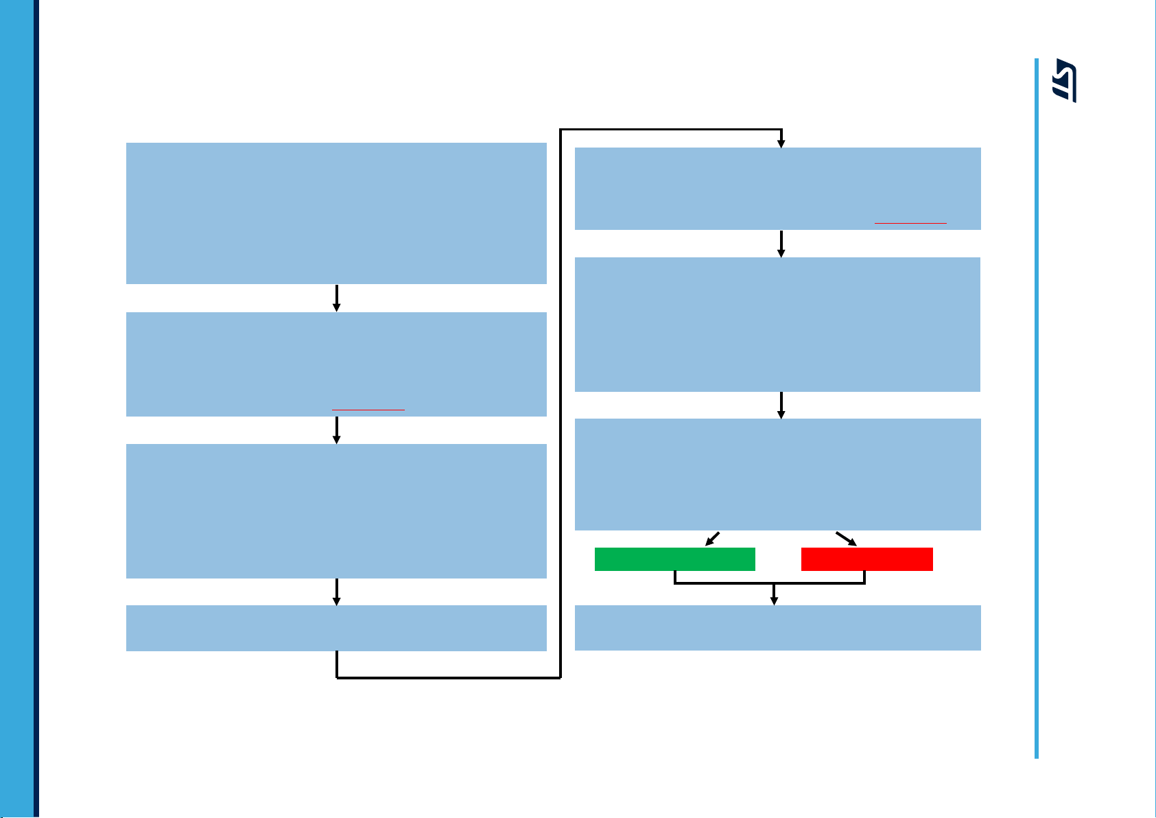
The embedded self-test functions allow checking device functionality without moving it.
When the accelerometer self-test is enabled, an actuation force is applied to the sensor, leading to a deflection
of the moveable part of the sensor. In this case the sensor outputs exhibit a change in their DC levels which are
related to the selected full scale through the sensitivity value.
The accelerometer self-test function is off when the ST[2:1] bits of the CTRL3 register are programmed to 00b; it
is enabled when the ST[2:1] bits are set to 01b (positive sign self-test) or 10b (negative sign self-test).
When the accelerometer self-test is activated, the sensor output level is given by the algebraic sum of the data
produced by the electrostatic test-force and gravity.
The procedure consists of:
1. enabling the accelerometer
2. averaging five samples before enabling the self-test
3. averaging five samples after enabling the self-test
4. computing the difference in absolute value for each axis and verifying that it falls within a given range. The
min and max values are provided in the datasheet.
The complete accelerometer self-test procedure is indicated in Figure 16. Accelerometer self-test procedure.
Notes:
1. Keep the device still during the self-test procedure.
2. The full scale and data rate used in the self-test procedure are not mandatory but recommended.
3. Please refer to the datasheet for minimum and maximum values.
AN5326
Self-test
AN5326 - Rev 3
page 35/42
Page 36
Wait 100 ms for stable output
Check DRDY in STATUS (27h) – Data-Ready bit
Reading OUTX/OUTY/OUTZ clears DRDY, wait for the first sample
Read OUT_X_L(28h), OUT_X_H(29h), OUT_Y_L(2Ah), OUT_Y_H(2Bh),
OUT_Z_L(2Ch), OUT_Z_H(2Dh)
Discard data
Check DRDY in STATUS (27h) – Data-Ready bit
Reading OUTX/OUTY/OUTZ clears DRDY, wait for the first sample
Read OUT_X_L(28h), OUT_X_H(29h), OUT_Y_L(2Ah),
OUT_Y_H(2Bh), OUT_Z_L(2Ch), OUT_Z_H(2Dh)
Discard data
YES (PASS) NO (FAIL)
Write 00h to CTRL1 (20h): Disable sensor
Write 00h to CTRL3 (22h): Disable self-test
Read the output registers after checking DRDY bit *5 times
Read OUT_X_L (28h), OUT_X_H (29h): Store data in OUTX_NOST
Read OUT_Y_L (2Ah), OUT_Y_H (2Bh): Store data in OUTY_NOST
Read OUT_Z_L (2Ch), OUT_Z_H (2Dh): Store data in OUTZ_NOST
The 14-bit left-justified data is expressed in two’s complement.
Average the stored data on each axis.
Write 40h to CTRL3 (22h) Enable self-test
Wait 100 ms for stable output
|Min(ST_X)| <=|OUTX_ST-OUTX_NOST| <= |Max(ST_X)|
AND
|Min(ST_Y)<=|OUTY_ST-OUTY_NOST| <= |Max(ST_Y)|
AND
|Min(ST_Z)| <=|OUTZ_ST-OUTZ_NOST| <=|MAX(ST_Z)|
Read the output registers after checking DRDY bit * 5 times
Read OUT_X_L (28h), OUT_X_H (29h): Store data in OUTX_ST
Read OUT_Y_L (2Ah), OUT_Y_H (2Bh): Store data in OUTY_ST
Read OUT_Z_L (2Ch), OUT_Z_H (2Dh): Store data in OUTZ_ST
The 14-bit left-justified data is expressed in two’s complement.
Average the stored data on each axis
Write 0Ch to CTRL2 (21h)
Write 00h to CTRL3 (22h)
Write 00h to CTRL4_INT1 (23h)
Write 00h to CTRL5_INT2 (24h)
Write 10h to CTRL6 (25h)
Write 43h to CTRL1 (20h)
Initialize sensor, turn on sensor
Set BDU=1, FS=4g, Power Mode 4, ODR=50Hz
AN5326
- Rev 3
Figure 16. Accelerometer self-test procedure
page 36/42
Note: The wait time of 100 ms is not mandatory but recommended. In any case, the settling time should be taken into account.
AN5326
Page 37

Revision history
Table 28. Document revision history
Date Version Changes
13-Aug-2019 1 Initial release
Updated pin status of pin 1 and pin 4 in Table 1. Pin description
Updated Section 3.3 Single data conversion (on-demand mode)
Updated Figure 3. Accelerometer filtering chain diagram
Updated Section 4.1 Startup sequence
Updated Section 4.3 Using the data-ready signal
Updated Section 5 Interrupt generation and embedded functions
Updated Section 5.1 Interrupt pin configuration
14-Aug-2020 2
21-Jan-2021 3
Updated Section 5.3 Free-fall interrupt
Updated Section 5.4 Wake-up interrupt
Updated Section 5.5.1 6D orientation detection
Updated Section 5.6 Activity/Inactivity recognition
Updated Section 6.5 Retrieving data from FIFO
Updated Section 7 Temperature sensor
Updated Table 27. Content of output data registers vs. temperature
Minor textual changes
Updated Section 3.5 High-pass filter configuration
Updated Section 5.3 Free-fall interrupt
AN5326
AN5326 - Rev 3
page 37/42
Page 38

AN5326
Contents
Contents
1 Pin description ....................................................................2
2 Registers ..........................................................................3
3 Operating modes ..................................................................5
3.1 Power mode...................................................................5
3.2 Continuous conversion ..........................................................6
3.3 Single data conversion (on-demand mode) .........................................7
3.4 Accelerometer bandwidth........................................................8
3.5 High-pass filter configuration ....................................................10
4 Reading output data ..............................................................11
4.1 Startup sequence .............................................................11
4.2 Using the status register........................................................11
4.3 Using the data-ready signal .....................................................11
4.4 Using the block data update (BDU) feature ........................................12
4.5 Understanding output data......................................................12
4.5.1 Example of output data ...................................................13
5 Interrupt generation and embedded functions.....................................14
5.1 Interrupt pin configuration ......................................................15
5.2 Event status ..................................................................16
5.3 Free-fall interrupt ..............................................................17
5.4 Wake-up interrupt .............................................................18
5.5 6D/4D orientation detection .....................................................20
5.5.1 6D orientation detection ..................................................20
5.5.2 4D orientation detection ..................................................22
5.6 Activity/Inactivity recognition ....................................................22
5.7 Stationary/Motion detection .....................................................24
5.8 Boot status ...................................................................24
6 First-in first-out (FIFO) buffer .....................................................25
6.1 FIFO description ..............................................................25
6.2 FIFO registers ................................................................26
AN5326 - Rev 3
page 38/42
Page 39

AN5326
Contents
6.2.1 FIFO_CTRL (2Eh).......................................................26
6.2.2 FIFO_SAMPLES (2Fh) ...................................................27
6.3 FIFO interrupts ...............................................................28
6.3.1 FIFO threshold .........................................................28
6.3.2 FIFO full ..............................................................28
6.3.3 FIFO overrun...........................................................28
6.4 FIFO modes..................................................................28
6.4.1 Bypass mode ..........................................................28
6.4.2 FIFO mode ............................................................29
6.4.3 Continuous mode .......................................................30
6.4.4 Continuous-to-FIFO mode.................................................31
6.4.5 Bypass-to-Continuous mode ...............................................32
6.5 Retrieving data from FIFO ......................................................33
7 Temperature sensor ..............................................................34
7.1 Example of temperature data calculation ..........................................34
8 Self-test ..........................................................................35
Revision history .......................................................................37
Contents ..............................................................................38
List of tables ..........................................................................40
List of figures..........................................................................41
AN5326 - Rev 3
page 39/42
Page 40

AN5326
List of tables
List of tables
Table 1. Pin description......................................................................2
Table 2. Registers .........................................................................3
Table 3. Accelerometer resolution ..............................................................5
Table 4. CTRL1 register ..................................................................... 5
Table 5. Operating mode selection ..............................................................5
Table 6. Power mode selection ................................................................5
Table 7. Output data rate selection ..............................................................6
Table 8. Single data conversion: typical time of conversion ............................................. 7
Table 9. Low-pass filter 1 bandwidth .............................................................8
Table 10. Bandwidth: low-pass path ..............................................................9
Table 11. Bandwidth: high-pass path ............................................................. 9
Table 12. Sensitivity ........................................................................ 12
Table 13. CTRL4_INT1...................................................................... 15
Table 14. CTRL5_INT2...................................................................... 16
Table 15. Free-fall threshold value .............................................................. 17
Table 16. SIXD_SRC register ................................................................. 20
Table 17. Threshold for 4D/6D function ........................................................... 20
Table 18. SIXD_SRC register for 6D positions ......................................................21
Table 19. Pulse duration on interrupt pin ..........................................................22
Table 20. FIFO buffer full representation (32nd sample set stored) ........................................ 25
Table 21. FIFO buffer full representation (33rd sample set stored and 1st sample discarded) ...................... 25
Table 22. FIFO_CTRL register................................................................. 26
Table 23. FIFO_SAMPLES register ............................................................. 27
Table 24. FIFO_SAMPLES behavior assuming FTH[4:0] = 15 ...........................................27
Table 25. Example: threshold function of ODR ...................................................... 33
Table 26. Temperature sensor characteristics ...................................................... 34
Table 27. Content of output data registers vs. temperature ............................................. 34
Table 28. Document revision history ............................................................. 37
AN5326 - Rev 3
page 40/42
Page 41

AN5326
List of figures
List of figures
Figure 1. Pin connections ...................................................................2
Figure 2. Single data conversion using INT2 as external trigger (SLP_MODE_SEL = 0) ........................7
Figure 3. Accelerometer filtering chain diagram ....................................................8
Figure 4. High-pass filter in normal and reference mode ............................................. 10
Figure 5. Data-ready signal ................................................................. 12
Figure 6. Embedded functions ............................................................... 14
Figure 7. Interrupt pin configuration ........................................................... 15
Figure 8. Free-fall interrupt ................................................................. 17
Figure 9. Wake-up event recognition (using the HP filter)............................................. 19
Figure 10. 6D recognized orientations........................................................... 21
Figure 11. Activity/Inactivity recognition (using the HP filter)............................................ 23
Figure 12. FIFO mode behavior ...............................................................29
Figure 13. Continuous mode with interrupt trigger................................................... 30
Figure 14. Continuous-to-FIFO mode: interrupt latched and non-latched ................................... 31
Figure 15. Bypass-to-Continuous mode .........................................................32
Figure 16. Accelerometer self-test procedure...................................................... 36
AN5326 - Rev 3
page 41/42
Page 42

AN5326
IMPORTANT NOTICE – PLEASE READ CAREFULLY
STMicroelectronics NV and its subsidiaries (“ST”) reserve the right to make changes, corrections, enhancements, modifications, and improvements to ST
products and/or to this document at any time without notice. Purchasers should obtain the latest relevant information on ST products before placing orders. ST
products are sold pursuant to ST’s terms and conditions of sale in place at the time of order acknowledgement.
Purchasers are solely responsible for the choice, selection, and use of ST products and ST assumes no liability for application assistance or the design of
Purchasers’ products.
No license, express or implied, to any intellectual property right is granted by ST herein.
Resale of ST products with provisions different from the information set forth herein shall void any warranty granted by ST for such product.
ST and the ST logo are trademarks of ST. For additional information about ST trademarks, please refer to www.st.com/trademarks. All other product or service
names are the property of their respective owners.
Information in this document supersedes and replaces information previously supplied in any prior versions of this document.
© 2021 STMicroelectronics – All rights reserved
AN5326 - Rev 3
page 42/42
 Loading...