

Page 1

Introduction
UM2271
User manual
Discovery kit with STM32L4R9AI MCU
The 32L4R9IDISCOVERY kit is a complete demonstration and development platform for the
STMicroelectronics Arm
Leveraging the innovative ultra-low power oriented features, 640
graphics performance (Chrom-ART Accelerator™) and DSI controller offered by the
STM32L4R9AI, the 32L4R9IDISCOVERY kit enables users to easily prototype applications
with state-of-the-art energy efficiency, as well as providing stunning audio and graphics
rendering with direct support for an AMOLED DSI round display. For even more userfriendliness, the on-board ST-LINK/V2-1 debugger provides out-of-the-box programming
and debugging capabilities.
The STM32L4R9AI microcontroller features four I2Cs, five USARTs, one ULP UART, three
SPIs, two SAIs, one SDIO, one USB 2.0 full-speed OTG, two CANs, one FMC parallel
synchronous interface, one 12-bit ADC, one 12-bit DAC, two ULP analog comparators, two
op amps, one 2 data-lane DSI display, one digital filter for sigma delta modulator and SWP
interface, two Octo-SPI interfaces, 8- to 14-bit camera interface, one touch sensing
controller interface, JTAG and SWD debugging support.
This Discovery board offers everything required for users to get started quickly and develop
applications easily.The hardware features on the board help to evaluate the following
peripherals: USB OTG FS, microSD™ card, 8-bit camera interface, 16-Mbit PSRAM, PMOD
and STMod+ connectors, IDD measurement, full-duplex I2S with an audio codec and stereo
headset jack including an analog microphone, DFSDM with a pair of MEMS digital
microphones on board, 512-Mbit Octo-SPI Flash memory device, I2C extension connector,
1.2" AMOLED display using a one data-lane DSI interface with a capacitive touch panel.
The Arduino™ compatible connectors expand the functionality with a wide choice of
specialized shields. The integrated ST-LINK/V2-1 provides an embedded in-circuit
debugger and programmer for the STM32 MCU.
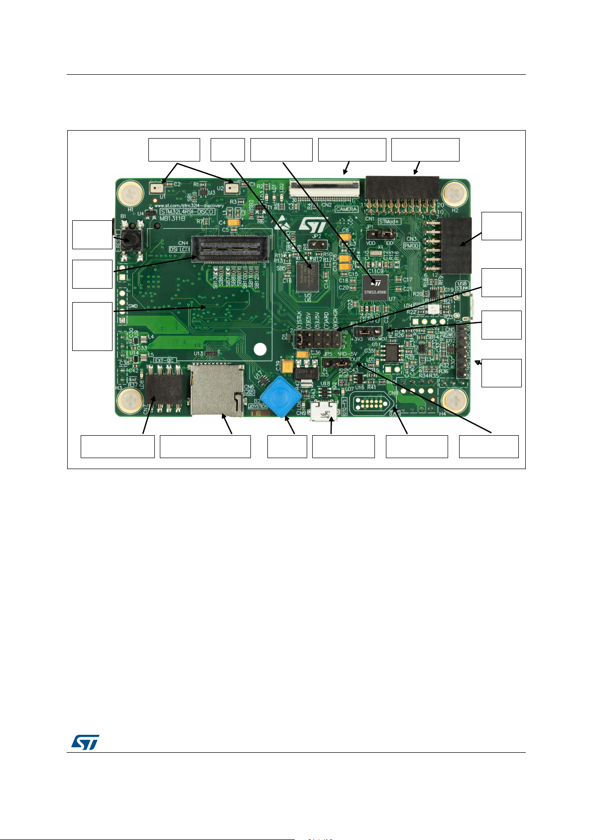
Figure 1. 32L4R9IDISCOVERY top view Figure 2. 32L4R9IDISCOVERY bottom view
®
Cortex®-M4 core-based STM32L4R9AI microcontroller.
Kbytes of embedded RAM,
Pictures are not contractual
October 2017 DocID030906 Rev 2 1/78
www.st.com
1
Page 2

Contents UM2271
Contents
1 Features . . . . . . . . . . . . . . . . . . . . . . . . . . . . . . . . . . . . . . . . . . . . . . . . . . . 7
2 Product marking . . . . . . . . . . . . . . . . . . . . . . . . . . . . . . . . . . . . . . . . . . . . 7
3 System requirements . . . . . . . . . . . . . . . . . . . . . . . . . . . . . . . . . . . . . . . . 8
4 Development toolchains . . . . . . . . . . . . . . . . . . . . . . . . . . . . . . . . . . . . . . 8
5 Demonstration software . . . . . . . . . . . . . . . . . . . . . . . . . . . . . . . . . . . . . . 8
6 Ordering information . . . . . . . . . . . . . . . . . . . . . . . . . . . . . . . . . . . . . . . . 8
7 Technology partners . . . . . . . . . . . . . . . . . . . . . . . . . . . . . . . . . . . . . . . . . 9
8 Bootloader limitations . . . . . . . . . . . . . . . . . . . . . . . . . . . . . . . . . . . . . . 10
9 AMOLED display limitation . . . . . . . . . . . . . . . . . . . . . . . . . . . . . . . . . . 11
10 Hardware layout and configuration . . . . . . . . . . . . . . . . . . . . . . . . . . . . 11
10.1 32L4R9IDISCOVERY layout . . . . . . . . . . . . . . . . . . . . . . . . . . . . . . . . . . 13
10.2 32L4R9IDISCOVERY mechanical drawing . . . . . . . . . . . . . . . . . . . . . . . 15
10.3 Embedded ST_LINK/V2-1 . . . . . . . . . . . . . . . . . . . . . . . . . . . . . . . . . . . . 16
10.3.1 Drivers . . . . . . . . . . . . . . . . . . . . . . . . . . . . . . . . . . . . . . . . . . . . . . . . . . 17
10.3.2 ST-LINK/V2-1 firmware upgrade . . . . . . . . . . . . . . . . . . . . . . . . . . . . . . 17
10.4 Low-power consumption status . . . . . . . . . . . . . . . . . . . . . . . . . . . . . . . . 17
10.5 TAG and SWD . . . . . . . . . . . . . . . . . . . . . . . . . . . . . . . . . . . . . . . . . . . . . 18
10.6 Power supply . . . . . . . . . . . . . . . . . . . . . . . . . . . . . . . . . . . . . . . . . . . . . . 19
10.6.1 Power supply sources . . . . . . . . . . . . . . . . . . . . . . . . . . . . . . . . . . . . . . 19
10.6.2 MCU power supply options . . . . . . . . . . . . . . . . . . . . . . . . . . . . . . . . . . 21
10.6.3 Supplying 32L4R9IDISCOVERY through ST-LINK/V2-1 USB . . . . . . . . 21
10.6.4 Measurement of MCU current consumption . . . . . . . . . . . . . . . . . . . . . 22
10.6.5 Program or debug when power supply not from ST-LINK/V2-1 . . . . . . . 23
10.7 Clock sources . . . . . . . . . . . . . . . . . . . . . . . . . . . . . . . . . . . . . . . . . . . . . . 23
10.8 Reset Source . . . . . . . . . . . . . . . . . . . . . . . . . . . . . . . . . . . . . . . . . . . . . . 23
2/78 DocID030906 Rev 2
Page 3

UM2271 Contents
10.9 Boot configuration . . . . . . . . . . . . . . . . . . . . . . . . . . . . . . . . . . . . . . . . . . 24
10.10 Audio codec . . . . . . . . . . . . . . . . . . . . . . . . . . . . . . . . . . . . . . . . . . . . . . . 24
10.11 DFSDM . . . . . . . . . . . . . . . . . . . . . . . . . . . . . . . . . . . . . . . . . . . . . . . . . . . 24
10.12 PSRAM . . . . . . . . . . . . . . . . . . . . . . . . . . . . . . . . . . . . . . . . . . . . . . . . . . . 25
10.13 USB OTG FS . . . . . . . . . . . . . . . . . . . . . . . . . . . . . . . . . . . . . . . . . . . . . . 25
10.13.1 32L4R9IDISCOVERY as USB device . . . . . . . . . . . . . . . . . . . . . . . . . . 25
10.13.2 32L4R9IDISCOVERY as USB host . . . . . . . . . . . . . . . . . . . . . . . . . . . . 26
10.14 Octo-SPI Flash memory . . . . . . . . . . . . . . . . . . . . . . . . . . . . . . . . . . . . . . 26
10.15 Virtual COM port . . . . . . . . . . . . . . . . . . . . . . . . . . . . . . . . . . . . . . . . . . . . 26
10.16 Buttons and LEDs . . . . . . . . . . . . . . . . . . . . . . . . . . . . . . . . . . . . . . . . . . 26
11 Connectors . . . . . . . . . . . . . . . . . . . . . . . . . . . . . . . . . . . . . . . . . . . . . . . 28
11.1 Arduino connectors CN10, CN11, CN16 and CN17 . . . . . . . . . . . . . . . . . 28
11.2 DSI display, backlight and touch panel connector CN4 . . . . . . . . . . . . . . 30
11.2.1 DSI AMOLED display . . . . . . . . . . . . . . . . . . . . . . . . . . . . . . . . . . . . . . 32
11.2.2 Backlight and OLED power supplies generation . . . . . . . . . . . . . . . . . . 32
11.2.3 Touch panel . . . . . . . . . . . . . . . . . . . . . . . . . . . . . . . . . . . . . . . . . . . . . . 32
11.3 USB OTG FS connector CN9 . . . . . . . . . . . . . . . . . . . . . . . . . . . . . . . . . . 33
11.4 ST-LINK/V2-1 USB Micro-B connector CN13 . . . . . . . . . . . . . . . . . . . . . 33
11.5 microSD card connector CN6 . . . . . . . . . . . . . . . . . . . . . . . . . . . . . . . . . . 34
11.6 STMod+ connector CN1 . . . . . . . . . . . . . . . . . . . . . . . . . . . . . . . . . . . . . . 35
11.7 PMOD connector CN3 . . . . . . . . . . . . . . . . . . . . . . . . . . . . . . . . . . . . . . . 37
11.8 Camera module connector CN2 . . . . . . . . . . . . . . . . . . . . . . . . . . . . . . . . 38
11.9 TAG connector CN8 . . . . . . . . . . . . . . . . . . . . . . . . . . . . . . . . . . . . . . . . . 39
11.10 SWD header CN5 . . . . . . . . . . . . . . . . . . . . . . . . . . . . . . . . . . . . . . . . . . . 39
11.11 EXT_I2C connector CN7 . . . . . . . . . . . . . . . . . . . . . . . . . . . . . . . . . . . . . 40
11.12 Stereo headset and headphone jack CN12 . . . . . . . . . . . . . . . . . . . . . . . 41
Appendix A GPIO assignment and sharing . . . . . . . . . . . . . . . . . . . . . . . . . . . . . 42
Appendix B Solder bridges . . . . . . . . . . . . . . . . . . . . . . . . . . . . . . . . . . . . . . . . . . 50
Appendix C STMod+ GPIO sharing and multiplexing . . . . . . . . . . . . . . . . . . . . . 52
Appendix D Schematics. . . . . . . . . . . . . . . . . . . . . . . . . . . . . . . . . . . . . . . . . . . . . 54
DocID030906 Rev 2 3/78
4
Page 4

Contents UM2271
Appendix E Fanout board (MB1280) . . . . . . . . . . . . . . . . . . . . . . . . . . . . . . . . . . . 71
E.1 MikroElektronika mikroBUS™ compatible connector
(Fanout CN10 / CN11). . . . . . . . . . . . . . . . . . . . . . . . . . . . . . . . . . . . . . . . 71
E.2 ESP-01 Wi-Fi
®
board compatible connector. . . . . . . . . . . . . . . . . . . . . . . 72
E.3 Compatible connectors for the Grove boards . . . . . . . . . . . . . . . . . . . . . . 72
E.3.1 Compatible connector for I2C Grove boards (Fanout CN3) . . . . . . . . . . 72
E.3.2 Compatible connector for UART Grove boards (Fanout CN2) . . . . . . . . 73
Appendix F Federal Communications Commission (FCC) and Industry Canada
(IC) Compliance74
F.1 FCC Compliance Statement . . . . . . . . . . . . . . . . . . . . . . . . . . . . . . . . . . . 74
F.1.1 Part 15.19 . . . . . . . . . . . . . . . . . . . . . . . . . . . . . . . . . . . . . . . . . . . . . . . . 74
F.1.2 Part 15.105 . . . . . . . . . . . . . . . . . . . . . . . . . . . . . . . . . . . . . . . . . . . . . . . 74
F.1.3 Part 15.21 . . . . . . . . . . . . . . . . . . . . . . . . . . . . . . . . . . . . . . . . . . . . . . . . 74
F.2 IC Compliance Statement . . . . . . . . . . . . . . . . . . . . . . . . . . . . . . . . . . . . . 74
F.2.1 Compliance Statement . . . . . . . . . . . . . . . . . . . . . . . . . . . . . . . . . . . . . . 74
F.2.2 Déclaration de conformité. . . . . . . . . . . . . . . . . . . . . . . . . . . . . . . . . . . . 74
Appendix G CISPR32 . . . . . . . . . . . . . . . . . . . . . . . . . . . . . . . . . . . . . . . . . . . . . . . 76
G.1 Warning. . . . . . . . . . . . . . . . . . . . . . . . . . . . . . . . . . . . . . . . . . . . . . . . . . . 76
Revision history . . . . . . . . . . . . . . . . . . . . . . . . . . . . . . . . . . . . . . . . . . . . . . . . . . . . 77
4/78 DocID030906 Rev 2
Page 5

UM2271 List of tables
List of tables
Table 1. Ordering information . . . . . . . . . . . . . . . . . . . . . . . . . . . . . . . . . . . . . . . . . . . . . . . . . . . . . . . 9
Table 2. JP10: VDD_STL setting . . . . . . . . . . . . . . . . . . . . . . . . . . . . . . . . . . . . . . . . . . . . . . . . . . . 18
Table 3. SW1 switch setting . . . . . . . . . . . . . . . . . . . . . . . . . . . . . . . . . . . . . . . . . . . . . . . . . . . . . . . 18
Table 4. 32L4R9IDISCOVERY power sources configuration . . . . . . . . . . . . . . . . . . . . . . . . . . . . . . 19
Table 5. JP4: power source selector setting. . . . . . . . . . . . . . . . . . . . . . . . . . . . . . . . . . . . . . . . . . . 20
Table 6. JP5: ARD 5 V input/output voltage selection setting . . . . . . . . . . . . . . . . . . . . . . . . . . . . . 21
Table 7. JP7: VDD setting . . . . . . . . . . . . . . . . . . . . . . . . . . . . . . . . . . . . . . . . . . . . . . . . . . . . . . . . 21
Table 8. JP1: IDD_MCU measurement setting. . . . . . . . . . . . . . . . . . . . . . . . . . . . . . . . . . . . . . . . . 22
Table 9. JP3: VDDA and VDDUSB, settings . . . . . . . . . . . . . . . . . . . . . . . . . . . . . . . . . . . . . . . . . . 22
Table 10. Boot modes. . . . . . . . . . . . . . . . . . . . . . . . . . . . . . . . . . . . . . . . . . . . . . . . . . . . . . . . . . . . . 24
Table 11. LD1 and LD2 details . . . . . . . . . . . . . . . . . . . . . . . . . . . . . . . . . . . . . . . . . . . . . . . . . . . . . . 27
Table 12. Buttons and LEDs . . . . . . . . . . . . . . . . . . . . . . . . . . . . . . . . . . . . . . . . . . . . . . . . . . . . . . . . 27
Table 13. Arduino compatible connectors . . . . . . . . . . . . . . . . . . . . . . . . . . . . . . . . . . . . . . . . . . . . . 28
Table 14. JP3, VDDA and VDDUSB, settings . . . . . . . . . . . . . . . . . . . . . . . . . . . . . . . . . . . . . . . . . . 29
Table 15. DSI display connector CN4. . . . . . . . . . . . . . . . . . . . . . . . . . . . . . . . . . . . . . . . . . . . . . . . . 30
Table 16. USB OTG FS Micro-AB connector CN9 . . . . . . . . . . . . . . . . . . . . . . . . . . . . . . . . . . . . . . . 33
Table 17. USB Micro-B connector CN13 . . . . . . . . . . . . . . . . . . . . . . . . . . . . . . . . . . . . . . . . . . . . . . 34
Table 18. microSD connector CN6 . . . . . . . . . . . . . . . . . . . . . . . . . . . . . . . . . . . . . . . . . . . . . . . . . . . 35
Table 19. STMod+ connector CN1 . . . . . . . . . . . . . . . . . . . . . . . . . . . . . . . . . . . . . . . . . . . . . . . . . . . 36
Table 20. Quad SPDT switch configuration . . . . . . . . . . . . . . . . . . . . . . . . . . . . . . . . . . . . . . . . . . . . 36
Table 21. PMOD connector CN3 . . . . . . . . . . . . . . . . . . . . . . . . . . . . . . . . . . . . . . . . . . . . . . . . . . . . 37
Table 22. Camera module connector CN2 . . . . . . . . . . . . . . . . . . . . . . . . . . . . . . . . . . . . . . . . . . . . . 38
Table 23. TAG connector CN8 . . . . . . . . . . . . . . . . . . . . . . . . . . . . . . . . . . . . . . . . . . . . . . . . . . . . . . 39
Table 24. SWD header CN5 . . . . . . . . . . . . . . . . . . . . . . . . . . . . . . . . . . . . . . . . . . . . . . . . . . . . . . . . 40
Table 25. EXT_I2C connector CN7 . . . . . . . . . . . . . . . . . . . . . . . . . . . . . . . . . . . . . . . . . . . . . . . . . . 40
Table 26. I2C1 addresses (on board) . . . . . . . . . . . . . . . . . . . . . . . . . . . . . . . . . . . . . . . . . . . . . . . . . 40
Table 27. Audio jack connector CN12 . . . . . . . . . . . . . . . . . . . . . . . . . . . . . . . . . . . . . . . . . . . . . . . . 41
Table 28. 32L4R9IDISCOVERY GPIO assignment and sharing . . . . . . . . . . . . . . . . . . . . . . . . . . . . 42
Table 29. MFX_V3 GPIO assignment (LQFP48) . . . . . . . . . . . . . . . . . . . . . . . . . . . . . . . . . . . . . . . . 48
Table 30. 32L4R9IDISCOVERY solder bridges . . . . . . . . . . . . . . . . . . . . . . . . . . . . . . . . . . . . . . . . . 50
Table 31. STMod+ GPIO sharing and multiplexing . . . . . . . . . . . . . . . . . . . . . . . . . . . . . . . . . . . . . . 52
Table 32. SPDT quad switch . . . . . . . . . . . . . . . . . . . . . . . . . . . . . . . . . . . . . . . . . . . . . . . . . . . . . . . 53
Table 33. Description of the mikroBUS connectors (CN11 and CN10) . . . . . . . . . . . . . . . . . . . . . . . 72
Table 34. Description of the ESP-01 Wi-Fi board connector pins. . . . . . . . . . . . . . . . . . . . . . . . . . . . 72
Table 35. Description of the I2C Grove board connector pins (CN3) . . . . . . . . . . . . . . . . . . . . . . . . . 73
Table 36. Description of the UART Grove board connector pins (CN2) . . . . . . . . . . . . . . . . . . . . . . . 73
Table 37. Document revision history . . . . . . . . . . . . . . . . . . . . . . . . . . . . . . . . . . . . . . . . . . . . . . . . . 77
DocID030906 Rev 2 5/78
5
Page 6

List of figures UM2271
List of figures
Figure 1. 32L4R9IDISCOVERY top view . . . . . . . . . . . . . . . . . . . . . . . . . . . . . . . . . . . . . . . . . . . . . . . 1
Figure 2. 32L4R9IDISCOVERY bottom view . . . . . . . . . . . . . . . . . . . . . . . . . . . . . . . . . . . . . . . . . . . . 1
Figure 3. Hardware block diagram. . . . . . . . . . . . . . . . . . . . . . . . . . . . . . . . . . . . . . . . . . . . . . . . . . . 12
Figure 4. 32L4R9IDISCOVERY top side layout . . . . . . . . . . . . . . . . . . . . . . . . . . . . . . . . . . . . . . . . . 13
Figure 5. 32L4R9IDISCOVERY bottom side layout . . . . . . . . . . . . . . . . . . . . . . . . . . . . . . . . . . . . . . 14
Figure 6. 32L4R9IDISCOVERY mechanical drawing (top view, in mm) . . . . . . . . . . . . . . . . . . . . . . 15
Figure 7. 32L4R9IDISCOVERY mechanical drawing (bottom view, in mm) . . . . . . . . . . . . . . . . . . . 16
Figure 8. How to update driver software . . . . . . . . . . . . . . . . . . . . . . . . . . . . . . . . . . . . . . . . . . . . . . 17
Figure 9. JP4 default configuration . . . . . . . . . . . . . . . . . . . . . . . . . . . . . . . . . . . . . . . . . . . . . . . . . . 19
Figure 10. DSI display connector CN4. . . . . . . . . . . . . . . . . . . . . . . . . . . . . . . . . . . . . . . . . . . . . . . . . 30
Figure 11. USB OTG FS Micro-AB connector CN9 . . . . . . . . . . . . . . . . . . . . . . . . . . . . . . . . . . . . . . . 33
Figure 12. USB Micro-B connector CN13 . . . . . . . . . . . . . . . . . . . . . . . . . . . . . . . . . . . . . . . . . . . . . . 34
Figure 13. microSD connector CN6 (top view) . . . . . . . . . . . . . . . . . . . . . . . . . . . . . . . . . . . . . . . . . . 35
Figure 14. STMod+ connector CN1 . . . . . . . . . . . . . . . . . . . . . . . . . . . . . . . . . . . . . . . . . . . . . . . . . . . 36
Figure 15. PMOD connector CN3 . . . . . . . . . . . . . . . . . . . . . . . . . . . . . . . . . . . . . . . . . . . . . . . . . . . . 37
Figure 16. Camera module connector CN2 . . . . . . . . . . . . . . . . . . . . . . . . . . . . . . . . . . . . . . . . . . . . . 38
Figure 17. TAG connector CN8 . . . . . . . . . . . . . . . . . . . . . . . . . . . . . . . . . . . . . . . . . . . . . . . . . . . . . . 39
Figure 18. EXT_I2C connector CN7 . . . . . . . . . . . . . . . . . . . . . . . . . . . . . . . . . . . . . . . . . . . . . . . . . . 40
Figure 19. Stereo headset with microphone jack CN12. . . . . . . . . . . . . . . . . . . . . . . . . . . . . . . . . . . . 41
Figure 20. 32L4R9IDISCOVERY board interconnections (MB1311C) . . . . . . . . . . . . . . . . . . . . . . . . 55
Figure 21. 32L4R9IDISCOVERY power . . . . . . . . . . . . . . . . . . . . . . . . . . . . . . . . . . . . . . . . . . . . . . . 56
Figure 22. 32L4R9IDISCOVERY Arduino Uno V3 connectors . . . . . . . . . . . . . . . . . . . . . . . . . . . . . . 57
Figure 23. 32L4R9IDISCOVERY ST-LINK/V2-1 . . . . . . . . . . . . . . . . . . . . . . . . . . . . . . . . . . . . . . . . . 58
Figure 24. 32L4R9IDISCOVERY Octo-SPI Flash memory . . . . . . . . . . . . . . . . . . . . . . . . . . . . . . . . . 59
Figure 25. 32L4R9IDISCOVERY peripherals . . . . . . . . . . . . . . . . . . . . . . . . . . . . . . . . . . . . . . . . . . . 60
Figure 26. 32L4R9IDISCOVERY USB OTG FS . . . . . . . . . . . . . . . . . . . . . . . . . . . . . . . . . . . . . . . . . 61
Figure 27. 32L4R9IDISCOVERY Round DSI display interface . . . . . . . . . . . . . . . . . . . . . . . . . . . . . . 62
Figure 28. 32L4R9IDISCOVERY IDD measurement and Multi Function eXpander . . . . . . . . . . . . . . 63
Figure 29. 32L4R9IDISCOVERY microcontroller . . . . . . . . . . . . . . . . . . . . . . . . . . . . . . . . . . . . . . . . 64
Figure 30. 32L4R9IDISCOVERY PSRAM . . . . . . . . . . . . . . . . . . . . . . . . . . . . . . . . . . . . . . . . . . . . . . 65
Figure 31. 32L4R9IDISCOVERY camera . . . . . . . . . . . . . . . . . . . . . . . . . . . . . . . . . . . . . . . . . . . . . . 66
Figure 32. 32L4R9IDISCOVERY STMOD+ interface . . . . . . . . . . . . . . . . . . . . . . . . . . . . . . . . . . . . . 67
Figure 33. 32L4R9IDISCOVERY Audio and DFSDM . . . . . . . . . . . . . . . . . . . . . . . . . . . . . . . . . . . . . 68
Figure 34. Round DSI display board (MB1314) . . . . . . . . . . . . . . . . . . . . . . . . . . . . . . . . . . . . . . . . . . 69
Figure 35. Fanout board (MB1280) . . . . . . . . . . . . . . . . . . . . . . . . . . . . . . . . . . . . . . . . . . . . . . . . . . . 70
Figure 36. STMod+ Fanout module plugged into CN1 connector . . . . . . . . . . . . . . . . . . . . . . . . . . . . 71
6/78 DocID030906 Rev 2
Page 7

UM2271 Features
1 Features
• STM32L4R9AI Arm-based microcontroller with 2-Mbyte Flash memory and 640-Kbyte
RAM in UFBGA169 package
• 1.2" 390x390 pixel AMOLED round display panel with 16 million colors depth, MIPI
interface and capacitive touch panel
• USB OTG FS
• On-board current measurement
• SAI audio codec
• ST-MEMS digital microphones
• 16-Mbit asynchronous PSRAM
• 512-Mbit Octo-SPI Flash
• 2 user LEDs
• 1 reset push-button
• 4-direction joystick with selection button
• Board connectors:
– 8-bit camera
– USB OTG FS with Micro-AB
– Stereo headset jack including analog microphone input
– microSD card
• Board expansion connectors:
– Arduino Uno V3
–STMod+
–PMOD
– EXT_I2C
• Flexible power-supply options:
–ST-LINK USB V
• On-board ST-LINK/V2-1 debugger/programmer with USB
re-enumeration capability: mass storage, virtual COM port and debug port
• Comprehensive free software libraries and examples available with the STM32Cube
package
• Support of a wide choice of integrated development environments (IDEs), including
IAR™, Keil
®
and GCC-based IDEs
or external sources
BUS
®
DSI
2 Product marking
Evaluation tools marked as “ES” or “E” are not yet qualified and are therefore not ready to
be used as reference design or in production. Any consequences arising from such usage
DocID030906 Rev 2 7/78
77
Page 8

System requirements UM2271
will not be at ST’s charge. In no event will ST be liable for any customer usage of these
engineering sample tools as reference designs or in production.
‘E’ or ‘ES’ marking examples of location:
• on the targeted STM32 that is soldered on the board (for illustration of STM32 marking,
refer to the section ‘Package information’ of the STM32 datasheet at www.st.com).
• next to the evaluation tool ordering part number, that is stuck or silkscreen printed on
the board
This board features a specific STM32 device version which allows the operation of any
stack or library. This STM32 device shows a "U" marking option at the end of the standard
part number and is not available for sales.
3 System requirements
• Windows® OS (7, 8 and 10), Linux® 64-bit or macOS
• USB Type-A to Micro-B cable
4 Development toolchains
• Keil MDK-ARM
• IAR EWARM
• GCC-based IDEs including free SW4STM32 from AC6
(a)
(a)
5 Demonstration software
The demonstration software, included in the STM32Cube package corresponding to the onboard MCU, is preloaded in the STM32 Flash memory for easy demonstration of the device
peripherals in standalone mode. The latest versions of the demonstration source code and
associated documentation can be downloaded from the www.st.com/stm32l4-discovery web
page.
®
6 Ordering information
To order the 32L4R9IDISCOVERY kit, refer to Table 1.
a. On Windows only
8/78 DocID030906 Rev 2
Page 9

UM2271 Technology partners
Order code Target STM32
STM32L4R9I-DISCO STM32L4R9AII6
Table 1. Ordering information
7 Technology partners
MACRONIX:
512-Mbit Octo-SPI NOR Flash memory device, part number MX25LM51245GXDI00
GOVISIONOX OPTOELECTRONICS:
1.2 inch 390x390 AMOLED display, part number G1120TB103GF-001
DocID030906 Rev 2 9/78
77
Page 10

Bootloader limitations UM2271
8 Bootloader limitations
Boot from system Flash memory results in executing bootloader code stored in the system
Flash memory protected against writing and erasing. This allows in-system programming
(ISP), that is, flashing the STM32 user Flash memory. It also allows writing data into RAM.
The data come in via one of communication interfaces such as USART, SPI, I2C bus, USB
or CAN.
Bootloader version is identified by reading the bootloader ID at the address 0x1FFF6FFE.
Its value is 0x91 for bootloader V9.1 and 0x92 for V9.2.
The STM32L4R9AII6 part soldered on the 32L4R9IDISCOVERY main board is marked with
a date code corresponding to its date of manufacturing. STM32L4R9AII6 parts with a date
code prior or equal to week 37 of 2017 are fitted with bootloader V9.1 affected by the
limitations to be worked around, as described hereunder. Parts with the date code starting
from week 38 of 2017 contain bootloader V9.2 in which the limitations no longer exist.
To locate the visual date code information on the STM32L4R9II6 package, refer to its
datasheet (DS12023) available at www.st.com, section Package Information. Date code
related portion of the package marking takes Y WW format, where Y is the last digit of the
year and WW is the week. For example, a part manufactured in week 38 of 2017 bares the
date code 7 38.
There is also another mean to identify the need for workaround: before opening the blister of
the Discovery Kit, just check the back side of the blister. At the bottom left side, if the
reference number is equal or higher than 32L4R9IDISCO/ 02-0, it means the bootloader
version is V9.2 and there is no need to apply workaround. Any other inferior number like 010 will need the workaround.
Bootloader ID for the bootloader V9.1 is 0x91.
The following limitation exists in the bootloader V9.1:
Some user Flash memory data get corrupted when written via SPI interface
Description:
During bootloader SPI Write Flash operation, some random 64-bits (2 double-words) may
be left blank at 0xFF
Workarounds:
WA1: add a delay between sending Write command and its ACK request. Its duration
should be the duration of the 256-Byte Flash write time.
WA2: read back after each write operation (256 bytes or at end of user code flashing) and in
case of error start write again.
WA3: Using bootloader, load a patch code in RAM to write in Flash memory through same
Write Memory write protocol as bootloader (code provided by ST). The patch code is
available for download from www.st.com website with a readme.txt file containing usage
instructions.
10/78 DocID030906 Rev 2
Page 11

UM2271 AMOLED display limitation
9 AMOLED display limitation
Warning: Permanent image sticking may occur if AMOLED displays
same image for an extended period of time.
10 Hardware layout and configuration
32L4R9IDISCOVERY board is designed around the STM32L4R9AI (169 ball UFBGA
package DSI version). The hardware block diagram
between STM32L4R9AI and peripherals (PSRAM, Octo-SPI Flash, DSI color display, USB
OTG connector, USART, audio, camera connector, STMod+ and PMOD connectors, IDD
measurement, joystick, microSD card, I
embedded ST-LINK).
board. Mechanical drawing for 32L4R9IDISCOVERY and round DSI display boards is
described in
Figure 6.
Figure 4 and Figure 5 help the user to locate these features on the
2
C extension connector, Arduino Uno shields and
Figure 3 illustrates the connection
DocID030906 Rev 2 11/78
77
Page 12

Hardware layout and configuration UM2271
06Y9
*3,2
)0&
6:'
2FWR63,0B3
6'00&
3:5
86$57
63,
,&
86$57
'6,
'&0,
')6'0
57&+6(
,&
/38$57
6$,
27*
$5'FRQQHFWRU
302'
670RG
5HVHWEXWWRQ
-R\VWLFN
567Q*3,2
670/5$,
6(/
6(/
0ELW
DV\QFKURQRXV
365$0
99
SRZHUVXSSO\
67/,1.9
.+]FU\VWDO
0+]FU\VWDO
0ELW2FWR63,
)ODVKPHPRU\
7$*FRQQHFWRU
6:'FRQQHFWRU
0(0V
PLFURSKRQHV
8VHU/('
(;7B,&
FRQQHFWRU
0);9,''
PHDVXUHPHQW
/&'WRXFKSDQHO
'6,9FRQQHFWRU
8VHU/('
$XGLRFRGHF
DPSOLILHU
6WHUHRMDFNZLWK
PLFURSKRQH
&DPHUD
FRQQHFWRU
PLFUR6'
86%27*
FRQQHFWRU
Figure 3. Hardware block diagram
12/78 DocID030906 Rev 2
Page 13
UM2271 Hardware layout and configuration
06Y9
88
0LFURSKRQHV
8
365$08670/5$,,
&1
&DPHUDFRQQHFWRU
&1
670RGFRQQHFWRU
&1
302'
FRQQHFWRU
-3
3RZHU
KHDGHU
-3
9''$B
9''86%
&1
6:'
FRQQHFWRU
-3
$5'B,1287
&1
7$*FRQQHFWRU
&1
(;7B,&FRQQHFWRU
&1
PLFUR6'FDUGFRQQHFWRU
%
-R\VWLFN
&1
86%27*)6
%
5HVHW
&1
'6,9
FRQQHFWRU
0%
'6,
GLVSOD\
ERDUG
SODFH
10.1 32L4R9IDISCOVERY layout
Figure 4. 32L4R9IDISCOVERY top side layout
DocID030906 Rev 2 13/78
77
Page 14

Hardware layout and configuration UM2271
06Y9
&1&1$UGXLQRFRQQHFWRUV
&1
$XGLR
MDFN
8
$XGLR
FRGHF
-3
9''
-3
9
SRZHU
/('
8
2FWR63,
)ODVK
PHPRU\
&1
86%
67/,1.
8
67/,1.
0&8
-3
966B67/.
6:6ZLWFK &1&1$UGXLQRFRQQHFWRUV 80);H[SDQGHU
Figure 5. 32L4R9IDISCOVERY bottom side layout
14/78 DocID030906 Rev 2
Page 15

UM2271 Hardware layout and configuration
10.2 32L4R9IDISCOVERY mechanical drawing
Figure 6. 32L4R9IDISCOVERY mechanical drawing (top view, in mm)
Legend:
= Indicates the mounting hole between the 32L4R9IDISCOVERY board (at the top of Figure 6) and
the round DSI display board (at the bottom of Figure 6)
DocID030906 Rev 2 15/78
77
Page 16

Hardware layout and configuration UM2271
Figure 7. 32L4R9IDISCOVERY mechanical drawing (bottom view, in mm)
Plastic spacer height = 13 mm, overall height = 26 mm ± 1 mm
10.3 Embedded ST_LINK/V2-1
The ST-LINK/V2-1 programming and debugging tool is integrated on the
32L4R9IDISCOVERY board. Compared to ST-LINK/V2, the changes are listed below:
• new features supported on ST-LINK/V2-1:
– USB software re-enumeration
– Virtual Com port interface on USB
– Mass storage interface on USB
– USB power management request for more than 100 mA power on USB
• features no more supported on ST-LINK/V2-1:
–SWIM interface
– Application voltage lower than 3 V
For general information concerning the debugging and programming features that are
common to both versions V2 and V2-1, refer to ST-LINK/V2 in-circuit
debugger/programmer.
16/78 DocID030906 Rev 2
Page 17

UM2271 Hardware layout and configuration
10.3.1 Drivers
Before connecting the 32L4R9IDISCOVERY to a Windows (7, 8, 10) PC via USB, a driver
for ST-LINK/V2-1 must be installed. It is available on the www.st.com website.
If 32L4R9IDISCOVERY is connected to the PC before the driver is installed, some
interfaces of the board may be declared as ‘Unknown’ in the PC device manager. In this
case the user must install the driver files, and update the driver of the connected device
from the device manager as shown on
Note: Prefer using the ‘USB Composite Device’ handle for a full recovery.
Figure 8. How to update driver software
Figure 8: How to update driver software
10.3.2 ST-LINK/V2-1 firmware upgrade
The ST-LINK/V2-1 embeds a firmware upgrade mechanism for in-situ upgrade through the
USB port. As the firmware may evolve during the life time of the ST-LINK/V2-1 product
(such as new functionality, bug fixes or support for new microcontroller families), it is
recommended to visit www.st.com before starting to use the 32L4R9IDISCOVERY and
periodically, in order to stay up-to-date with the latest firmware version.
10.4 Low-power consumption status
There is a way to make the board get into very low power consumption status in which the
current on +5
1. The connections between ST-LINK/V2-1 and MCU must be disconnected by micro
switch SW1 manually (see
ARD-5V IN position. Remove JP10. Then, connect an external 5 V power supply on
CN16 pin 5 5V and on GND.
2. Peripherals (including display, CTP and PSRAM) are powered off by MOSFET which is
controlled by MFX_GPIO8 / MFX_aGPIO2 (put them as input floating), and by setting
V can be below 20 uA. How to get into the low power mode:
Tabl e 3 below). Set JP4 on (7) ARD position, and put JP5 in
DocID030906 Rev 2 17/78
77
Page 18

Hardware layout and configuration UM2271
21
21
all peripherals related I/Os to inactive level (input pull-down or input is good option
according to I/Os).
3. Disconnect JP9 to remove +5 V from LD8 power LED, disconnect JP10 (or put it in 2-3
position), power off OCTOSPI (remove SB23/SB24) and configure related I/Os as input
pull down.
4. Peripherals can be setup by FW to reach power down mode. All I/Os must be
configured in non-consuming states. Set MFX_V3 to sleep mode, get SD card out of its
socket slot. Set the Audio Codec in power down.
10.5 TAG and SWD
One TAG interface footprint CN8 is reserved on 32L4R9IDISCOVERY and is usable to
debug and program the on-board MCU.
Note: Micro switch SW1 must be put in Off position. R24 and R31 must be disconnected.
The SWD 6-pin header CN5 added on 32L4R9IDISCOVERY, connected to on board STLINK MCU, is usable to debug and program an external MCU.
VDD from the external board is 1.8 V or 3.3 V, thanks to the on board voltage converter.
Table 2. JP10: VDD_STL setting
Jumper Setting Description
Default setting.
VDD_STL gets power from 32L4R9IDISCOVERY. ST-LINK is
JP10
then usable to program the on-board MCU.
VDD_STL gets power from external through CN5. ST-LINK is
then usable to program an external MCU.
SW1 is accessible on bottom side of 32L4R9IDISCOVERY. By default, SW1 is in On
position. To put micro switch in Off position, just push away the switch from ON position as
shown in
Tabl e 3.
Table 3. SW1 switch setting
Switch Setting Description
Default setting.
SW1 switch is On.
SW1
SW1 is Off.
18/78 DocID030906 Rev 2
Page 19
UM2271 Hardware layout and configuration
06Y9
10.6 Power supply
10.6.1 Power supply sources
32L4R9IDISCOVERY is designed to be powered by +5 V DC power supply. It is possible to
configure the 32L4R9IDISCOVERY to use any of the sources listed in
By default, the JP4 header must have a jumper on (1) STLK and SW1 is placed in ON
position. Any JP4 position different from (1) STLK requires SW1 to be placed in OFF
position (see
Tabl e 3).
Table 4. 32L4R9IDISCOVERY power sources configuration
Tabl e 4.
JP4 configuration
(function)
(1) STLK (USB_STLINK) CN5 (VBUS) 5 V 500 mA
(3) E5V (ARDUINO) CN16 (VIN) 6 V - 9 V => 5 V
(5) U5V (USB_OTG_FS) CN8 (VBUS) 5 V 500 mA
(7) ARD (ARDUINO) CN16 (ARD-5V)
(9) CHGR (USB_STLINK) CN5 (VBUS) 5 V
1. ARD-5V is a power output pin to Arduino connector CN16 (default) or a power input pin from Arduino
connector CN16, according to JP5 setting. See Table 6 below.
Power source
connector (pin name)
(1)
Voltage Available current
Arduino Uno V3 shield
dependent
5 V
Arduino Uno V3 shield
dependent
Power supply
dependent
Note: 32L4R9IDISCOVERY must be powered by a power-supply unit or by an auxiliary equipment
complying with the standard EN-60950-1: 2006+A11/2009, and must be safety extra low
voltage (SELV) with limited power capability.
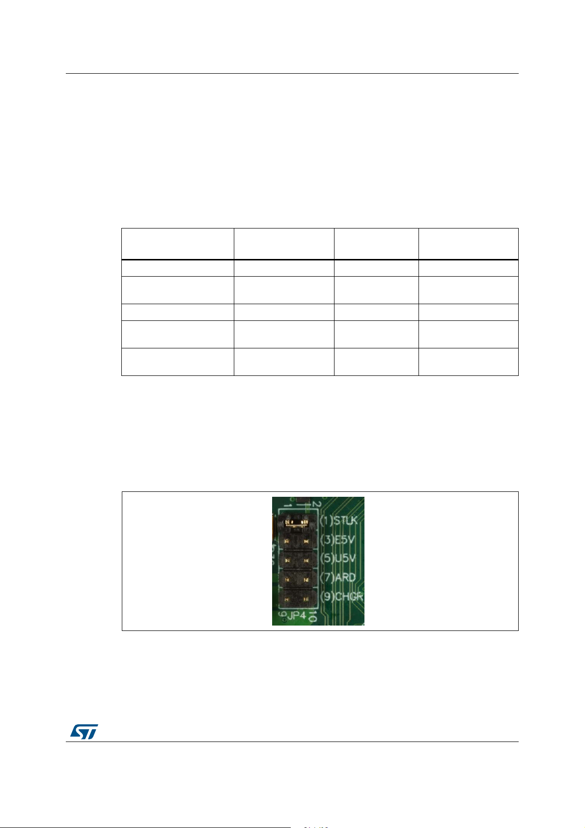
Figure 9 shows a physical description of the 10-pin header JP4 default configuration.
Figure 9. JP4 default configuration
Detailed description of all JP4 possible configurations are listed below and in Ta b le 5:
• STLK: 5 V from the ST-LINK/V2-1 USB connector CN13 with 500 mA current limitation.
Power mechanism of supplying the board by STLINK/V2-1 is explained Section 10.6.3.
DocID030906 Rev 2 19/78
77
Page 20

Hardware layout and configuration UM2271
67/.
(9
89 $5' &+*5
67/.
(9
89 $5' &+*5
67/.
(9
89 $5' &+*5
67/.
(9
89 $5' &+*5
67/.
(9
89 $5' &+*5
A jumper must be placed in location STLK of JP4, connecting pins 1 and 2. The green
LED LD8 is lit on to confirm presence of 5 V voltage.
• E5V: 5 V from the 6 V to 9 V DC from VIN pin of Arduino compatible connector CN16
(the U15 regulator is converting VIN into a 5 V voltage). The VIN input voltage is limited
to 9 V to keep temperature of the regulator U15 within its thermal safe area. A jumper
must be placed connecting pins 3 and 4 of JP4. The green LED LD8 is lit on to confirm
presence of 5 V voltage. SW1 must be placed in OFF position.
• U5V: 5 V from the 5 V DC of USB OTG FS user connector CN9. A jumper must be
placed in location USB of JP4, connecting pins 5 and 6.The green LED LD8 is lit on to
confirm presence of 5 V voltage. SW1 must be placed in OFF position.
• ARD: 5 V from the 5 V of Arduino compatible connector CN16. A jumper must be
placed in location ARD of JP4, connecting pins 7 and 8. The green LED LD8 is lit on to
confirm presence of 5 V voltage and at t the same time, pins 2 and 3 of JP5 must be
connected to get 5 V power from Arduino. SW1 must be placed in OFF position. In
case the main board provides 5 V to Arduino compatible connector CN16, which is the
default configuration, pins 1 and 2 of JP5 must be connected (see Tabl e 6 ).
• CHGR: 5 V from 5 V DC power charger connected to USB STLINK (CN13). In this
case, if 32L4R9IDISCOVERY is powered by an external USB charger, then the debug
on CN13 is not available. When CHGR input is chosen, it is not recommended to
connect a PC on USB STLINK, because the 500 mA limitation is no more effective and
this may damage the PC. A jumper must be placed in location CHGR of JP4,
connecting pins 9 and 10. The green LED LD8 is lit on to confirm presence of 5 V
voltage. SW1 must be placed in OFF position.
Table 5. JP4: power source selector setting
Jumper Setting Description
Default setting.
32L4R9IDISCOVERY is supplied though CN13 Micro-B
ST-LINK/V2-1 connector.
32L4R9IDISCOVERY is supplied though Arduino connector
CN16 (VIN).
JP4
32L4R9IDISCOVERY is supplied though USB OTG FS
connector CN9.
32L4R9IDISCOVERY powers ARDUINO or is supplied by
ARDUINO, according to JP5 setting in Tab l e 6 below.
32L4R9IDISCOVERY is supplied though CN13 Micro-B STLINK/V2-1 connector. In that case, the SB36 solder bridge must
be soldered.
20/78 DocID030906 Rev 2
Page 21

UM2271 Hardware layout and configuration
Table 6. JP5: ARD 5 V input/output voltage selection setting
Jumper Setting Description
Default setting.
32L4R9IDISCOVERY supplies 5 V to Arduino connector CN16.
JP5
32L4R9IDISCOVERY is supplied by 5 V from Arduino connector
CN16.
10.6.2 MCU power supply options
32L4R9IDISCOVERY offers possibility to supply the MCU under 1.8 V or 3.3 V. The JP7
jumper must be placed on +3V3 to supply the MCU with 3.3
jumper can be placed on +1V8 of JP7 to supply the MCU with 1.8
pins
2 and 3 (see Table 7).
Functions listed below are not compatible with the +1V8 setting of JP7:
• OCTOSPI
• PSRAM
• ARDUINO Uno Revision 3
• CAMERA
• microSD card
• ADC measurements (except if JP3 is set at +3V3, or except if VREF+ configuration is
changed)
• USB OTG FS (except if JP3 is set at +3V3)
Table 7. JP7: VDD setting
SW1 must be placed in OFF position.
V, connecting pins 1 and 2. The
V, connecting
Jumper Setting Description
Default setting.
VDD is powered from +3V3 regulator.
JP7
VDD is powered from +1V8 regulator.
10.6.3 Supplying 32L4R9IDISCOVERY through ST-LINK/V2-1 USB
To power the board through ST-LINK/V2-1, the USB host (a PC) must be connected with the
32L4R9IDISCOVERY standard Micro-B USB receptacle, via a USB cable. This event starts
the USB enumeration procedure. In its initial phase, the current supply capability of the USB
host port is limited to 100
32L4R9IDISCOVERY draws power at that time. If the solder bridge SB36 is open (default
setting), the U11 ST890 power switch is set to Off position, which isolates the remainder of
the board from the power source. In the next phase of the enumeration procedure, the host
PC informs the ST-LINK/V2-1 facility of its capability to supply up to 500
answer is positive, the ST-LINK/V2-1 sets the U11 ST890 switch to On position to supply
power to the remainder of the board. If the PC USB port is not capable of supplying up to
500
mA, another power source must be used like VIN pin of connector CN16.
mA. It is enough because only ST-LINK/V2-1 part of
mA current. If the
DocID030906 Rev 2 21/78
77
Page 22
Hardware layout and configuration UM2271
The ST890 power switch protects the host USB port against current demand exceeding
625
mA, in case a short circuit occurs on the board (the red LED fault LD5 lights on).
32L4R9IDISCOVERY can also be supplied by STLINK USB power source with no
enumeration, such as a USB charger. In this particular case, the SB36 solder bridge must
be closed. ST-LINK/V2-1 turns the ST890 power switch On regardless of enumeration
procedure result and passes the power unconditionally to the board. The green LED LD8
lights on whenever the whole board is powered.
10.6.4 Measurement of MCU current consumption
Jumper JP1 allows the consumption of STM32L4R9AI to be measured directly by a built-in
MCU current ammeter circuit (MFX_V3, able to measure from 60
removing the jumper and replace it by an external ammeter (see
To measure the MCU consumption in standby or shutdown modes, MFX_V3 needs to run
software. To wake up MCU from these modes, it is necessary to press the Reset button B1,
or to wait a few seconds.
Jumper Setting Description
JP1
Table 8. JP1: IDD_MCU measurement setting
Default setting.
A module on the board is designed to measure from 60 nA to
50 mA by using several MOSFET, and switching automatically
depending on the read value.
STM32L4R9AI is powered by VDD. MCU current measurement
is not possible
No jumper on JP1: an ammeter can be connected on
pins 2 and 3 to measure STM32L4R9AI current (if there is no
ammeter, STM32L4R9AI is not powered).
nA to 50 mA) or by
Table 8).
VDDA and VDDUSB power inputs from STM32L4R9AI can be connected to two different
power sources, +3V3 or VDD_MCU. These power inputs may be included or not in the IDD
current measurement of VDD_MCU, depending on the JP3 jumper configurations described
in
Tabl e 9.
Jumper Setting Description
JP3
22/78 DocID030906 Rev 2
Table 9. JP3: VDDA and VDDUSB, settings
Default setting.
VDDA and VDDUSB power pins of STM32L4R9AI are supplied
with +3V3. the IDD measurement does not include their current
consumption. USB OTG FS is functional even if JP7 is set on
+1V8.
VDDA and VDDUSB power pins of STM32L4R9AI are supplied
with VDD_MCU. The IDD measurement includes their current
consumption.
Page 23

UM2271 Hardware layout and configuration
10.6.5 Program or debug when power supply not from ST-LINK/V2-1
Before connecting the USB cable from ST-LINK/V2-1 CN13 to the PC, it is mandatory to
power the board using the user USB OTG FS connector CN9 or the VIN pin of Arduino
connector CN16. Proceeding this way ensures that the enumeration succeeds thanks to the
external power source.
The following power-sequence procedure must be respected:
1. Put a jumper in JP4 at location U5V to use power from user USB CN9 or at location
E5V to use power from VIN of Arduino connector CN16.
2. Connect the corresponding external power source.
3. Check the green LED LD8 is turned On.
4. Connect the PC to ST-LINK/V2-1 USB connector CN13.
If this order is not respected, the board may be powered by VBUS first from ST-LINK, and
the following risks may be encountered:
• If more than 500 mA current is needed by the board, PC may be damaged or current is
limited by PC. As a consequence the board is not powered correctly.
• 500 mA is requested at the enumeration, so there is a risk that the request is rejected
and enumeration does not succeed if PC cannot provide such current.
10.7 Clock sources
Two clock sources are used by STM32L4R9AI: one on LSE input and another on HSE input.
LSE clock source
The available clock source is X1, 32 kHz crystal for the STM32L4R9AI embedded RTC.
HSE clock source
The second clock source available by default is X2, 16 MHz crystal for the STM32L4R9AI
HSE system clock.
Note that another HSE clocking option is available on PCB: MCO output from STLINK MCU
to STM32L4R9AI HSE input. Please refer to
10.8 Reset Source
The general reset of 32L4R9IDISCOVERY is active low. The reset sources are listed below:
• Reset button B1
• Embedded ST-LINK/V2-1, SW1 micro-switch set to On (default setting)
• Arduino compatible connector CN16 pin 3
The general reset is connected to following peripheral reset functions:
• STM32L4R9AI MCU reset
• Octo-SPI Flash reset
• MFX_V3 reset
• Camera reset
Appendix B: Solder bridges.
DocID030906 Rev 2 23/78
77
Page 24

Hardware layout and configuration UM2271
10.9 Boot configuration
After reset, STM32L4R9AI boots from one of the three different embedded memory
locations, depending on BOOT0 and BOOT1 bits:
• Boot from the main Flash memory (MCU internal Flash). This is the default
configuration.
• Boot from the system memory ISP (in-system programming).
• Boot from the SRAM1.
On 32L4R9IDISCOVERY board, the boot configuration of the MCU is controlled by the
BOOT0 signal on PH3 pin.
BOOT0 is by default grounded through the R15 pull-down resistor.
It is possible to set BOOT0 high by removing resistor R15 and populating resistor R16 with
a 10K resistor.
Please check below Tab l e 10 for other boot modes.
Table 10. Boot modes
nBOOT1
FLASH_OPTR[23]
XX01
XX01
X1X0
0X11
00X0
1X11
10X0
nBOOT0
FLASH_OPTR[27]
10.10 Audio codec
A Cirrus codec CS42L51-CNZ U26 connected to the SAI1 interface of STM32L4R9AI offers
possibility to connect a stereo headphone or headset with a mono analog microphone.
BOOT0 pin
PH3
nSWBOOT0
FLASH_OPTR[26]
Boot Memory Space Alias
Main Flash memory is selected
as boot area
System memory is selected as
boot area
Main Flash memory is selected
as boot area
Embedded SRAM1 is selected
as boot area
Embedded SRAM1 is selected
as boot area
System memory is selected as
boot area
System memory is selected as
boot area
The I²C-bus addresses of CS42L51-CNZ are 0x95 and 0x94.
10.11 DFSDM
Two ST-MEMS MP34DT01TR digital microphones U1 and U2 are available on
32L4R9IDISCOVERY. The two microphones are located at a distance of 21
other. They are connected to the STM32 DFSDM by the PC2 port, generating the clock, and
24/78 DocID030906 Rev 2
mm from each
Page 25

UM2271 Hardware layout and configuration
by PB12 port, collecting the PDM interleaved data. These microphones are powered by
MIC_VDD (PH2 of STM32L4R9AI).
The two DFSDM interface signals (clock and data), are also accessible on the STMod+
connector CN1. Before using STMod+, the user must follow the recommendations below:
• If STMod+ pin 17 is used, SB1 (DOUT) must be disconnected first.
• If STMod+ pins 18 or 20 are used, MIC_VDD GPIO (PH2) must be activated at high
level first.
10.12 PSRAM
Two PSRAM footprints are supported on the design, both connected to STM32L4R9AI FMC
interface:
• A 16-Mbit asynchronous PSRAM (U5), using up to A19 address, is soldered by default.
Reference is IS66WV1M16EBLL-55BLI.
• A 32-Mbit synchronous PSRAM (U6), using up to A20 address, may be used.
Reference is IS66WVC2M16ECLL-7010BLI.
By default, this PSRAM (U6) is exclusive with CAMERA function (due to DCMI_D4
function multiplexed with A20 of MCU). In case CAMERA is used at the same time than
PSRAM, it is possible to change two solder bridges to deactivate A20 on PSRAM (tied
to high, usable density 16 Mbits) and DCMI_D4 is used for CAMERA.
Note: Limitation: the two PSRAM are not compatible with JP7 setting at +1V8.
See Appendix B: Solder bridges for possible PSRAM configuration change.
10.13 USB OTG FS
32L4R9IDISCOVERY supports USB OTG FS (full-speed) communication via the USB
Micro-AB connector (CN9) and USB power switch (U16) connected to VBUS. The board
can be powered by this USB connection at 5
A green LED LD6 is lit in one of the following cases:
• Power switch (U16) is On and 32L4R9IDISCOVERY works as a USB host
• VBUS is powered by another USB host when 32L4R9IDISCOVERY works as a USB
device.
The red LED LD7 is lit when over-current occurs.
10.13.1 32L4R9IDISCOVERY as USB device
When the board works as a USB device, it can be powered by the 5 V DC VBUS of this USB
OTG FS connection (jumper JP4 pins 5 and 6 must be connected in position U5V). The
green LEDs LD6 VBUS and LD8 PWR are lit on to confirm the 5
V DC with 625 mA current limitation.
V presence.
DocID030906 Rev 2 25/78
77
Page 26

Hardware layout and configuration UM2271
10.13.2 32L4R9IDISCOVERY as USB host
When the board works as a USB host, it supplies the 5 V to the USB peripheral using one of
the following sources:
• ST-LINK/V2-1 USB Micro-B connector CN13 (jumper put in STLK location of JP4)
• an external 5 V source connected to pin 5 of the Arduino connector CN16 (jumper put
in ARD location of JP4)
• an external source between 7 V and 11 V, connected to VIN pin of Arduino connector
CN16 (jumper put in E5V location of JP4)
The green LED LD8 is lit on to confirm the presence of the 5 V source.
The power switch STMPS2141STR is controlled by the port MFX_GPIO13 to deliver the 5 V
power to the USB device connected to the USB connector CN9. When MFX_GPIO13 is
pulled down to ground, the power switch is closed, and the green LED LD6 confirms the 5
presence for the USB device. The red LED LD7 FAULT is lit when an over-current occurs.
For more details please refer to Section 10.6: Power supply.
V
10.14 Octo-SPI Flash memory
A 512-Mbit Octo-SPI user Flash memory (MX25LM51245GXDI00 from MACRONIX) is
connected to OCTOSPIM_P2 interface of STM32L4R9AI. By default, OCTOSPI_RESET of
Flash memory has been connected to the general reset of 32L4R9IDISCOVERY.
See Appendix B: Solder bridges for possible Octo-SPI Flash configuration change.
Note: Limitation: the Octo-SPI Flash memory is not compatible with JP7 setting at +1V8.
10.15 Virtual COM port
The serial interface USART2 is directly available as a virtual COM port of the PC, connected
to the ST-LINK/V2-1 USB connector CN13. The virtual COM port settings are configured as
follow: 115200
bps, 8-bit data, no parity, one stop bit, no flow control.
10.16 Buttons and LEDs
The blue button B2 is a four-directions joystick with a selection mode when pressed in the
center. The logic state is high when one of the five-position switch (left, right, up, down,
selection) is pressed. The center position (Select function) is connected to a wake-up pin of
the microcontroller PC13. The other four directions are mapped on MFX GPIOs.
The black button B1 near the display is the Reset button. It is used to reset the board and
can wake-up MCU from standby and shutdown IDD measurement modes.
Two user LEDs located near the camera connector CN2 are available for the user (see
Figure 4): LD1, LD2, from left to right, with orange and green color respectively. To light on a
LED, a low logic state 0 must be written in the corresponding GPIO.
• LD1 (orange) is managed by MFX function
• LD2 (green) is managed by STM32L4R9AI main MCU
26/78 DocID030906 Rev 2
Page 27

UM2271 Hardware layout and configuration
Table 11. LD1 and LD2 details
LED MCU port control color
LD1 PB0 (MFX_GPIO0 from MFX) Orange
LD2 PH4 (from main MCU) Green
Other LEDs are present on the 32L4R9IDISCOVERY. Find below a summary list of all
buttons and LEDs, with their description.
Reference Color Function Comment
B1 black RESET For MCU, OCTO-SPI Flash, MFX_V3, CAMERA
B2 blue
LD1 orange USER1 MFX_GPIO0, PB0
LD2 green USER2 PH4
Table 12. Buttons and LEDs
SELECT with Wake-up alternate function, PC13
UP MFX_GPIO1, PB1
DOWN MFX_GPIO2, PB2
RIGHT MFX_GPIO3, PB3
LEFT MFX_GPIO4, PB4
LD3 green ARDUINO PB13
LD4 red/green ST-LINK COM Green during communication
LD5 red ST-LINK USB FAULT Current higher than 625 mA
LD6 green VBUS USB OTG FS Status also available on PA9
LD7 red USB OTG FS OVCR Overcurrent detection, also on MFX_GPIO14, PB14
LD8 green 5V POWER -
DocID030906 Rev 2 27/78
77
Page 28

Connectors UM2271
11 Connectors
11.1 Arduino connectors CN10, CN11, CN16 and CN17
CN10, CN11, CN16 and CN17 are female connectors compatible with Arduino Uno
Revision 3 standard. Most of shields designed for Arduino can fit to 32L4R9IDISCOVERY
board.
Left connectors Right connectors
Table 13. Arduino compatible connectors
CN No.
CN16
Power
Pin
No.
1 - - E5V test SPI2_SCK PB13 D13 6
2 IOREF - VDD SPI2_MISO PB14 D12 5
3 NRST NRST Reset
43V3 -
5 5V - 5Vinput/output TIM8_CH1N PH13 D9 2
6 GND - Ground - PH15 D8 1
7 GND - Ground -
8VIN -
1 A0 PA7 ADC1_IN12 TIM5_CH2 PA1 D5 6
Pin
Name
MCU
Pin
-
- TIM3_CH1 PB4 D6 7
Function Function
I2C3_SCL PG7 D15 10
I2C3_SDA PG8 D14 9
AVD D - AVDD 8
Ground - GND 7
TIM3_CH2,
SPI2_MOSI
3V3output
(note 1)
+6V to +9V
power input
(note 2)
TIM5_CH4,
SPI2_NSS
-
-PA4D78
MCU
Pin
PB15 D11 4
PI0 D10 3
Pin
Name
Pin
No.
CN No.
CN10
Digital
2 A1 PC4 ADC1_IN13 - PG6 D4 5
3 A2 PC3 ADC1_IN4 TIM15_CH2 PF10 D3 4
4 A3 PB0 ADC1_IN15 - PG11 D2 3
CN17
Analog
5A4
PA0 or
PG8
(note 3)
PA5 or
6A5
28/78 DocID030906 Rev 2
PG7
(note 3)
ADC1_IN5
or
I2C3_SDA
(note 3)
ADC1_IN10
or
I2C3_SCL
(note 3)
LPUART1_TX PC1 D1 2
LPUART1_RX PC0 D0 1
CN11
Digital
Page 29

UM2271 Connectors
1. The 3V3 on ARD connector PIN4 is not a power input for 32L4R9IDISCOVERY board, to simplify power architecture.
2. The external voltage applied to pin VIN should be in the range 6 to 9V at 25°C ambient temperature. If a higher voltage is
applied on the regulator U15, it may overheat and could be damaged.
3. By default, pin 5 and pin 6 of CN17 connector are connected to ADC MCU input ports PA0 and PA5 respectively, thanks to
configuration of solder bridges: SB33 and SB35 closed, SB32 and SB34 opened. In case it is necessary to connect I2C
interface signals on pins 5 and 6 of CN17 instead of ADC inputs, open SB33 and SB35, and close SB32 and SB34.
VREF+, the voltage reference used by the internal DAC and ADC of STM32L4R9AI, has
three different power sourcing capabilities:
• from STM32L4R9AI MCU Internal buffer generation (Default). VREFBUF internal ADC
/ DAC voltage reference is set to 2.5V by default.
• from an external Arduino shield, connected to connector CN10. In that case, SB27
needs to be connected to bring AVDD on VREF+, a 100nF is necessary on C48 and
VREFBUF needs to be de-activated.
• from a VDDA power supply generated on 32L4R9IDISCOVERY board. VDDA is also
connected to VDDUSB of STM32L4R9AI. In that case, mounting a 0 ohm resistor on
R14 is necessary. VREFBUF needs to be de-activated. A jumper JP3 also needs to be
set as below description.
Jumper Setting Description
Table 14. JP3, VDDA and VDDUSB, settings
Default setting.
JP3
Jumper on PIN1/2, VDDA get power from +3V3
VDDA
Setting
Jumper on PIN2/3, VDDA get power form VDD_MCU
(See warning below)
Warning: When VDDA=VDD_MCU and if VDD_MCU=1.8 V (check JP7
setting), there will be huge leakage current and a risk of
damaging MCU I/Os in case 3.3 V logic level is connected to
ADC input I/Os of STM32L4R9AI. Also, ADC measurements
will not be functional in default configuration
Caution: The I/Os of STM32 microcontroller are 3V3 compatible instead of 5 V for Arduino Uno.
Note: Limitation: the Arduino Uno Revision 3 is not compatible with JP7 setting at +1V8.
See Appendix B: Solder bridges for possible Arduino configuration change.
DocID030906 Rev 2 29/78
77
Page 30

Connectors UM2271
06Y9
ϭ
Ϯ
ϲϬ
ϱϵ
11.2 DSI display, backlight and touch panel connector CN4
All the necessary signals to interface with round DSI display board are available through the
DSI V3 connector CN4.
Figure 10. DSI display connector CN4
Function GPIO port Signal name
General ground - GND 1 2 NC - -
Differential DSI
clock
Differential DSI
clock
General ground - GND 7 8 DSI_D2_P -
Differential DSI
data 0
General ground - GND 13 14 DSI_D3_P -
Differential DSI
data 1
- DSI_CK_P 3 4 TOUCH_INT MFX_GPIO9
- DSI_CK_N 5 6 GND -
- DSI_D0_P 9 10 DSI_D2_N -
-DSI_D0_N1112GND -
- DSI_D1_P 15 16 DSI_D3_N -
-DSI_D1_N1718GND -
General ground - GND 19 20 NC - -
Power output - +5v 21 22 SPI_CS PH14
Table 15. DSI display connector CN4
CN6 pin
number
Signal name GPIO port Function
Touch panel
interrupt
General
ground
reference
Not
connected
Not
connected
General
ground
Not
connected
Not
connected
General
ground
SPI chip
select
30/78 DocID030906 Rev 2
Page 31

UM2271 Connectors
Table 15. DSI display connector CN4 (continued)
Function GPIO port Signal name
Power output - +5v 23 24 SPI2_SCK PB13 SPI clock
- - NC 25 26 SPI2_MOSIp PB15 SPI data
SM3321 ground - BLGND 27 28 SPI_DCX PB14
SM3321 ground - BLGND 29 30 NC - -
- - NC 31 32 RESERVED - -
- - NC 33 34 NC - -
- - NC 35 36 3V3 -
- - NC 37 38 VDDIO -
- - NC 39 40 I2C1_SDA PG13
- - NC 41 42 NC - -
DSI_SWIRE
control output
- - NC 45 46 NC - -
- - NC 47 48 NC - -
DSI tearing
effect input
PA8 DSI_SWIRE 43 44 I2C1_SCL PB6
PF11 TE 49 50 NC - -
CN6 pin
number
Signal name GPIO port Function
SPI
data/control
3V3 voltage
reference
IOVDD
reference
Touch panel
I2C data
Touch panel
I2C clock
- - NC 51 52 NC - -
DSI Backlight
control output
- - NC 55 56 NC - -
DSI and Touch
panel Reset
output
- - NC 59 60 1V8 -
General ground - GND 61 62 GND -
General ground - GND 63 64 GND -
PB1 DSI_BL_CTRL 53 54 NC - -
MFX_
GPIO10
DSI_RESET 57 58 NC - -
See Appendix B: Solder bridges for possible DSI display configuration change.
1.8V voltage
reference
General
ground
General
ground
DocID030906 Rev 2 31/78
77
Page 32

Connectors UM2271
11.2.1 DSI AMOLED display
Warning: Permanent image sticking may occur if AMOLED displays
same image for an extended period of time.
The DSI display is based on a round AMOLED Touch sensitive panel of 1.2 inch and
390x390
Optoelectronics. It displays up to 16M colors. The round DSI display module board
reference is MB1314. The DSI interface of MB1314 is only one data-lane width and a clock
lane, but the 32L4R9IDISCOVERY board supports DSI displays with up to two data-lane
width. The DSI_V3 connector interface also enables the use of dedicated low power modes
of display, thanks to the available SPI2 interface (MB1314 does not use it). It is also possible
to use some of USART3 signals to control a low power mode (SB6 and SB8 are respectively
exclusive with SB13 and SB7).
The DSI_TE signal PF11 is used as an input of the main microcontroller connected to the
display signal TE (tearing effect). DSI_TE signal is used to synchronize the refresh of the
display memory by the microcontroller with the display scan, this to avoid visible artefacts.
DSI_3V3_PWRON signal (MFX_GPIO8, low level active) controls the 3V3 level Power
supplies provided on the DSI_V3 connector interface. DSI_1V8_PWRON signal
(MFX_aGPIO2) controls the 1V8 level Power supplies provided on the DSI_V3 connector
interface. Both shall be used to enable or disable display, TP and PSRAM. They allows to
disconnect those peripherals when doing low power IDD measurement.
pixels. The display module reference is IEG1120TB103GF-001 from Govisionox
DSI_RESET signal (MFX_GPIO10, low level active) controls the reset for the display and
the Touch panel.
An optional DSI_SWIRE signal PA8 offers additional possibility to control the voltage for any
display supply during initialization (not used by MB1314 by default). PA8 is exclusive with
another function from 32L4R9IDISCOVERY board: CAMERA clock Interface (MCO), which
is the default setting.
11.2.2 Backlight and OLED power supplies generation
This function is handled by the Power driver circuit SM3321, included on the MB1314 DSI
display Board. SM3321 is a switching mode boost converter supplied by the 3V3 rail of the
DSI_V3 connector interface. SM3321 is controlled either by the AMOLED driver circuit itself
(default configuration), either by DSI_BL_CTRL (PB1) from main MCU, either from the
DSI_SWIRE (PA8) interface from main MCU. SM3321 provides all necessary voltage
references to AMOLED display.
If used, the signal DSI_BL_CTRL switches on the backlight with a high level. It is possible to
dim the backlight intensity by applying a low frequency PWM signal to DSI_BL_CTRL (1 to
10
kHz typically).
11.2.3 Touch panel
The touch panel is a capacitive touch panel using an I2C interface. The touch panel IC
reference is FT3267, and is located on the MB1314 board. The FT3267 I2C1 default
addresses are 0x71 and 0x70.
32/78 DocID030906 Rev 2
Page 33

UM2271 Connectors
06Y9
Touch panel interrupt output DSI_TOUCH_INT is connected to MFX_GPIO9. It is used as
touch panel detection indication. MFX_GPIO10 resets capacitive touch panel and DSI
display.
11.3 USB OTG FS connector CN9
An USB OTG full speed communication link is available at USB Micro AB receptacle
connector CN9. Micro AB receptacle enables USB Host and USB Device features.
MFX_GPIO13 is used to enable on-board VBUS power when in Host mode.
Figure 11. USB OTG FS Micro-AB connector CN9
Pin number Description Pin number Description
1 VBUS (PA9) 4 ID (PA10)
2DM (PA11) 5GND
3 DP (PA12) - -
Table 16. USB OTG FS Micro-AB connector CN9
11.4 ST-LINK/V2-1 USB Micro-B connector CN13
The USB connector CN13 is used to connect the embedded ST-LINK/V2-1 to the PC.
DocID030906 Rev 2 33/78
77
Page 34

Connectors UM2271
06Y9
Figure 12. USB Micro-B connector CN13
Pin number Description Pin number Description
1 VBUS (power) 4 GND
2 DM 5,6 Shield
3DP --
Table 17. USB Micro-B connector CN13
11.5 microSD card connector CN6
microSD cards with 4 GBytes or more capacity are inserted in the receptacle CN6. Four
data bits of the SDMMC1 interface, CLK and CMD signals of the STM32L4R9AI are used to
communicate with the microSD card at +3V3 only. The card insertion is detected by the
MFX_GPIO5: when a microSD card is inserted, the logic level is 0, otherwise it is 1.
34/78 DocID030906 Rev 2
Page 35

UM2271 Connectors
06Y9
Figure 13. microSD connector CN6 (top view)
Pin
number
1 SDMMC1_D2 (PC10) 6 GND
2 SDMMC1_D3 (PC11) 7 SDMMC1_D0 (PC8)
3 SDMMC1_CMD (PD2) 8 SDMMC1_D1 (PC9)
4 VDD (+3V3) 9 µSD_DETECT (MFX_GPIO5)
5 SDMMC1_CLK (PC12) 10-11-12 GND (casing)
Table 18. microSD connector CN6
Description
Pin
number
Note: Limitation: the microSD is not compatible with JP7 setting at +1V8.
11.6 STMod+ connector CN1
The standard 20-pin STMod+ connector is available on 32L4R9IDISCOVERY board to
increase compatibility with external boards and modules from the Ecosystem of
microcontrollers. By default, it is designed to support an ST dedicated Fanout board which
allows connecting different modules or board extensions from different manufacturers.
Fanout board also embeds a 3V3 regulator and I2C level shifters. Schematics of Fanout
board is available in
Figure 35.: Fanout board (MB1280). For more detailed information,
Description
DocID030906 Rev 2 35/78
77
Page 36

Connectors UM2271
06Y9
)URQWYLHZ
please refer to ST Fanout board user manual and to relevant datasheets of associated
modules.
For details about STMod+ interface, please refer to STMod+ connector interface
specification.
Figure 14. STMod+ connector CN1
Pin
number
Table 19. STMod+ connector CN1
Description
Pin
number
Description
1 SPI2_CS/USART3_CTS (PA6) 11 INT (PC6)
2 SPI2_MOSIp/USART3_TXD (PB15/PB10) 12 RST (PI7)
3 SPI2_MISOp/USART3_RXD (PB14/PB11) 13 ADC (PA4)
4 SPI2_SCK/USART3_RTS (PB13/PA15) 14 PWM (PA5)
5GND15+5V
6 +5V 16 GND
7 I2C3_SCL (PG7) 17 GPIO (PB12)
8 SPI2_MOSIs (PI3) 18 GPIO (PC2)
9 SPI2_MISOs (PI2) 19 GPIO (PC7)
10 I2C3_SDA (PG8) 20 GPIO (PC2)
In order to be able to support selection of SPI or UART functions connection on STMod+ by
software, a quad SPDT switch has been added. It is controlled by two GPIOs from MFX
circuit and enables MCU signal selection for pins 2, 3 and 4. By default, STMod+ connector
is selected, and STMOD+_SEL_0 and STMOD+_SEL_1 of MFX circuit are set to support
one of the STMod+ interface configuration.
Pin number SPI UART / SPI
Table 20. Quad SPDT switch configuration
(1)
UART
STMOD+_SEL_0 (GPIO6 of MFX_V3) 0 1 1
STMOD+_SEL_1 (GPIO7 of MFX_V3) 0 0 1
STMod+ pin 1 (directly connected to PA6) SPI_CS SPI_CS USART3_CTS
STMod+ pin 2 SPI2_MOSIp USART3_TX USART3_TX
36/78 DocID030906 Rev 2
Page 37

UM2271 Connectors
06Y9
)URQWYLHZ
Table 20. Quad SPDT switch configuration (continued)
Pin number SPI UART / SPI
STMod+ pin 3 SPI2_MISOp USART3_RX USART3_RX
STMod+ pin 4 SPI2_SCK SPI2_SCK USART3_RTS
1. UART / SPI defines default configuration for STMOD+_SEL_0 and STMOD+_SEL_1.
(1)
UART
Please, take care that this connector shares many GPIOs with other functions on the Board:
for more detailed information please refer to
Appendix A: GPIO assignment and sharing.
In addition, to have a quick look at STMod+ GPIO sharing and multiplexing, and to get a
quick view on other Alternate functions available on its pins, please refer to
Appendix C:
STMod+ GPIO sharing and multiplexing.
Note: Limitation: The STMod+ interface is not compatible with JP7 setting at +1V8.
Note: Limitation: if STMod+ pin 17 is used, please take care to disconnect SB1 first. If STMod+ pin
18/20 is used, please activate MIC_VDD GPIO (PH2) at high level first.
11.7 PMOD connector CN3
The standard 12-pin PMOD connector is available on STM32L4R9I-DISCO Discovery board
to support low frequency, low I/O pin count peripheral modules. The PMOD interface which
has been implemented on STM32L4R9I-DISCO Discovery board is compatible with the
PMOD type 2A & 4A I/O signal assignment convention.
Figure 15. PMOD connector CN3
Pin number Description Pin number Description
1 SPI2_CS/USART3_CTS (PA6) 7 INT (PC6)
2 SPI2_MOSIp/USART3_TXD (PB15/PB10) 8 RESET (PI7)
3 SPI2_MISOp/USART3_RXD (PB14/PB11) 9 NA
4 SPI2_SCK/USART3_RTS (PB13/PA15) 10 NA
5GND 11GND
Table 21. PMOD connector CN3
63V3 123V3
DocID030906 Rev 2 37/78
77
Page 38

Connectors UM2271
06Y9
In order to be able to support selection of SPI or UART functions connection on PMOD by
software, a quad SPDT switch has been added on board. It is controlled by two GPIOs from
MFX_V3 circuit and enables MCU signal choice for pins 2, 3 and 4: refer to
Tabl e 20
STMod+ chapter for switch description details (pin 1, 2, 3 and 4 of PMOD are common with
STMod+).
By default, STMod+ connector is selected, so STMOD+_SEL_0 and STMOD+_SEL_1
needs to be modified to support one of the PMOD interface configuration. Also, PMOD
shares GPIOs with other functions of the Board: for more detailed information please refer
to
Appendix A: GPIO assignment and sharing.
Note: Limitation: the PMOD interface is not compatible with JP7 setting at +1V8.
11.8 Camera module connector CN2
An 8-bit camera module function is supported thanks to the 30-pin dedicated ZIF connector
CN2. The reference of camera module to be used is STM32F4DIS-CAM. This module has
to be connected with caution before powering on the STM32L4R9I-DISCO Discovery board.
The camera module I²C addresses are 0x61 and 0x60. Camera can be used by default, but
one might take care about GPIO sharing and multiplexing with other function, in order to
program the good configuration. For more detailed information please refer to
GPIO assignment and sharing.
Appendix A:
Note: Limitation: the camera is not compatible with JP7 setting at +1V8.
Figure 16. Camera module connector CN2
Pin number Description Pin number Description
1GND 16GND
2 NC 17 DCMI_HSYNC (PA4)
3NC 18NC
4 DCMI_D0 (PC6) 19 DCMI_VSYNC (PI5)
5 DCMI_D1 (PC7) 20 VDD
6 DCMI_D2 (PH11) 21 DCMI_CLK (PA8)
Table 22. Camera module connector CN2
7 DCMI_D3 (PH12) 22 NC
8 DCMI_D4 (PE4) 23 GND
9 DCMI_D5 (PI4) 24 NC
38/78 DocID030906 Rev 2
Page 39

UM2271 Connectors
06Y9
Table 22. Camera module connector CN2 (continued)
Pin number Description Pin number Description
10 DCMI_D6 (PB8) 25 DCMI_PWR_EN (MFX_GPIO12)
11 DCMI_D7 (PI7) 26 DCMI_NRST (NRST from MCU)
12 NC 27 I2C1_SDA (PG13)
13 NC 28 I2C1_SCL (PB6)
14 GND 29 GND
15 DCMI_PIXCK (PH5) 30 VDD
11.9 TAG connector CN8
The TAG connector footprint CN8 is used to connect STM32L4R9AI microcontroller for
programming or debugging the board.
Figure 17. TAG connector CN8
Pin number Description Pin number Description
1 VDD 10 NRST (PH3, RESET#)
2 SWDIO (PA13) 9 NA
3GND 8NA
4 SWCLK (PA14) 7 NA
5GND 6SWO (PB3)
11.10 SWD header CN5
The 6-pin SWD header is used to program or debug an MCU in an external application
board using a dedicated cable connected to it. To use this SWD header interface, pins 2 and
3 of JP10 need to be connected with a jumper. Furthermore, SW1 must be set in OFF
position while R24 and R31 need to be disconnected.
By default, STLINK/V2-1 is used to program or debug on board MCU. Pin1 and 2 of JP10
are connected, SW1 is in ON position, R24 and R31 are connected.
Table 23. TAG connector CN8
DocID030906 Rev 2 39/78
77
Page 40

Connectors UM2271
06Y9
)URQWYLHZ
Table 24. SWD header CN5
Pin number Description Pin number Description
1 VDD 4 SWDIO (PA13)
2 SWCLK (PA14) 5 NRST
3GND 6SWO (PB3)
11.11 EXT_I2C connector CN7
The EXT_I2C connector socket is used to connect external modules to I2C1 interface or to
monitor the I2C1 interface.
Figure 18. EXT_I2C connector CN7
Table 25. EXT_I2C connector CN7
Pin number Description Pin number Description
1 I2C1_SDA (PG13) 5 +3V3
2NC 6NC
3 I2C1_SCL (PB6) 7 GND
4 EXT_RESET (MFX_GPIO11) 8 NC
As I2C1 is available for external use, it is important to note that those following I2C1
applications and addresses are already used on board:
Application
DSI display Touch Panel 0x71/0x70 400 kHz Default I2C address
Audio Codec 0x95/0x94 100 kHz Default I2C address
CAMERA 0x61/0x60 400 kHz For STM32F4DIS-CAM Module
MFX_V3 0x85/0x84 400 kHz Default I2C address
Table 26. I2C1 addresses (on board)
W/R I2C
address
I2C max. speed Comment
Depending on the I2C module plugged into CN7, I2C1 could even be used up to
Fast mode + (1 MHz).
40/78 DocID030906 Rev 2
Page 41

UM2271 Connectors
06Y9
ϯ
Ϯ
ϲ
ϰ
ϱ
ϭ
11.12 Stereo headset and headphone jack CN12
A stereo headphone or a stereo headset with analog microphone is pluggable into the
3.5
mm standard jack socket CN12.
Figure 19. Stereo headset with microphone jack CN12
Pin number Description Stereo headset with microphone pinning
6 OUT_Left SPK_L (33 ohms typ.)
4 OUT_Right SPK_R (33 ohms typ.)
3GND GND
2 IN_Analog Microphone
5NC
1NC
Table 27. Audio jack connector CN12
NA
If a headset is plugged into CN12, the bias of the microphone is driven by the output
MICBIAS1 of the codec and the analog audio enters into the codec by the pin AIN3A.
DocID030906 Rev 2 41/78
77
Page 42

42/78 DocID030906 Rev 2
Appendix A GPIO assignment and sharing
GPIO assignment and sharing UM2271
Table 28. 32L4R9IDISCOVERY GPIO assignment and sharing
Pin GPIO port GPIO primary interface STMod+ interface PMOD interface ARDUINO interface
K3 PA0 - - - ARD_A4 (ADC1_IN5)
M1 PA1 - - - ARD_D5 (TIM5_CH2)
N1 PA2 STLINK_USART2_TX - - -
M2 PA3 STLINK_USART2_RX - - -
N2 PA4
L3 PA5 -
L4 PA6 -
DCMI_HSYNC/DE STMod+_ADC (ADC_1_IN9) - ARD_D7
STMod+_PWM (TIM2_CH1) - ARD_A5 (ADC1_IN10)
STMod+_SPI2_CS //
STMod+_USART3_CTS
(NU)
PMOD_SPI2_CS //
PMOD_USART3_CTS
(NU)
-
M4 PA7 - - - ARD_A0 (ADC1_IN12)
(NU)
//
-- -
E11 PA8
DSI_SWIRE
DCMI_CLK (MC0)
E12 PA9 VBUS - - -
D11 PA10 ID - - -
E13 PA11 DM - - -
D13 PA12 DP - - -
A11 PA13 JTMS/SWDIO - - -
A10 PA14 JTCK/SWCLK - - -
A9 PA15 - STMod+_USART3_RTS
(NU)
(NU)
(NU)
//
--ARD_A3 (ADC1_IN15)
-- -
N4 PB0 DSI_USART3_CK
L5 PB1
DSI_BL_CTRL
DSI_SWIRE
(NU)
PMOD_USART3_RTS
(NU)
N5 PB2 MFX_WAKEUP_OUT - - -
-
Page 43

Table 28. 32L4R9IDISCOVERY GPIO assignment and sharing (continued)
Pin GPIO port GPIO primary interface STMod+ interface PMOD interface ARDUINO interface
A6 PB3 JTDO/TRACESWO - - -
A5 PB4 - - - ARD_D6 (TIM3_CH1)
B5 PB5 SAI1_SD_B - - -
C5 PB6 I2C1_SCL - - -
D5 PB7 PSRAM_NL (ADV) - - -
C4 PB8 DCMI_D6
(NU)
D4 PB9 SAI1_FS_A - - -
N9 PB10
DSI_USART3_TX
(NU)
STMod+_USART3_TX PMOD_USART3_TX -
-- -
UM2271 GPIO assignment and sharing
DocID030906 Rev 2 43/78
H7 PB11 -
N12 PB12
N13 PB13
M12 PB14
L10 PB15
DFSDM_1_DATIN1 STMod+_GPIO
DSI_SPI2_SCK
DSI_SPI_D/CX
DSI_SPI2_MOSI
(NU)
(NU)
(NU)
STMod+_USART3_RX PMOD_USART3_RX -
(NU)
--
STMod+_SPI2_SCK PMOD_SPI2_SCK ARD_D13 (SPI2_SCK)
STMod+_SPI2_MISOp
STMod+_SPI2_MOSIp
(NU)
(NU)
PMOD_SPI2_MISO
PMOD_SPI2_MOSI
(NU)
(NU)
ARD_D12 (SPI2_MISO)
ARD_D11 (SPI2_MOSI_TIM3_CH2)
J2 PC0 - - - ARD_D0 (LPUART1_RX)
J3 PC1 - - - ARD_D1 (LPUART1_TX)
J4 PC2
DFSDM_1_CKOUT STMod+_GPIO
(NU)
--
K1 PC3 - - - ARD_A2 (ADC1_IN4)
K4 PC4 - - - ARD_A1 (ADC1_IN13)
F11 PC6
G11 PC7
DCMI_D0 STMod+_INT PMOD_INT -
DCMI_D1 STMod+_GPIO - -
F9 PC8 SDMMC_1_D0 - - -
G13 PC9 SDMMC_1_D1 - - -
D9 PC10 SDMMC_1_D2 - - -
E9 PC11 SDMMC_1_D3 - - -
F8 PC12 SDMMC_1_CK - - -
Page 44

44/78 DocID030906 Rev 2
Table 28. 32L4R9IDISCOVERY GPIO assignment and sharing (continued)
Pin GPIO port GPIO primary interface STMod+ interface PMOD interface ARDUINO interface
E1 PC13 JOY_SEL // WAKEUP - - -
F1 PC14-OSC32_IN PC14-OSC32_IN - - -
GPIO assignment and sharing UM2271
G1
B8 PD0 PSRAM_D2 - - -
C8 PD1 PSRAM_D3 - - -
D8 PD2 SDMMC_1_CMD - - -
E8 PD3 PSRAM_CLK - - -
C7 PD4 PSRAM_NOE - - -
D7 PD5 PSRAM_NWE - - -
E7 PD6 PSRAM_NWAIT - - -
F7 PD7 PSRAM_NE1 - - -
K10 PD8 PSRAM_D13 - - -
K9 PD9 PSRAM_D14 - - -
J10 PD10 PSRAM_D15 - - -
J9 PD11 PSRAM_A16 - - -
J8 PD12 PSRAM_A17 - - -
H8 PD13 PSRAM_A18 - - -
H11 PD14 PSRAM_D0 - - -
H10 PD15 PSRAM_D1 - - -
A4 PE0 PSRAM_NBL0 - - -
B4 PE1 PSRAM_NBL1 - - -
PC15-
OSC32_OUT
PC15-OSC32_OUT - - -
D3 PE2 SAI1_MCLK_A - - -
D2 PE3 PSRAM_A19 - - -
D1 PE4
PSRAM_A20
(NU)
// DCMI_D4 - - -
Page 45

DocID030906 Rev 2 45/78
Table 28. 32L4R9IDISCOVERY GPIO assignment and sharing (continued)
Pin GPIO port GPIO primary interface STMod+ interface PMOD interface ARDUINO interface
E4 PE5 SAI1_SCK_A - - -
E3 PE6 SAI1_SD_A - - -
L7 PE7 PSRAM_D4 - - -
K6 PE8 PSRAM_D5 - - -
J6 PE9 PSRAM_D6 - - -
H6 PE10 PSRAM_D7 - - -
N8 PE11 PSRAM_D8 - - -
M8 PE12 PSRAM_D9 - - -
L8 PE13 PSRAM_D10 - - -
K7 PE14 PSRAM_D11 - - -
J7 PE15 PSRAM_D12 - - -
F5 PF0 PSRAM_A0 - - -
F4 PF1 PSRAM_A1 - - -
F3 PF2 PSRAM_A2 - - -
G3 PF3 PSRAM_A3 - - -
G4 PF4 PSRAM_A4 - - -
G5 PF5 PSRAM_A5 - - -
UM2271 GPIO assignment and sharing
H4 PF10 - - - ARD_D3 (TIM15_CH2)
M5 PF11 DSI_TE - - -
N6 PF12 PSRAM_A6 - - -
M6 PF13 PSRAM_A7 - - -
L6 PF14 PSRAM_A8 - - -
K5 PF15 PSRAM_A9 - - -
J5 PG0 PSRAM_A10 - - -
H5 PG1 PSRAM_A11 - - -
Page 46

46/78 DocID030906 Rev 2
Table 28. 32L4R9IDISCOVERY GPIO assignment and sharing (continued)
Pin GPIO port GPIO primary interface STMod+ interface PMOD interface ARDUINO interface
H9 PG2 PSRAM_A12 - - -
G8 PG3 PSRAM_A13 - - -
G7 PG4 PSRAM_A14 - - -
G9 PG5 PSRAM_A15 - - -
G12 PG6 - - - ARD_D4
GPIO assignment and sharing UM2271
G10 PG7 -
F10 PG8 -
B7 PG9 OCTOSPIM_P2_IO6 - - -
D6 PG10 OCTOSPIM_P2_IO7 - - -
E6 PG11 - - - ARD_D2
F6 PG12 OCTOSPIM_P2_NCS - - -
G6 PG13 I2C1_SDA - - -
C6 PG15 OCTOSPIM_P2_DQS - - -
H1 PH0-OSC_IN PH0-OSC_IN - - -
J1 PH1-OSC_OUT PH1-OSC_OUT - - -
A2 PH2 MIC_VDD - - -
E5 PH3-BOOT0 PH3-BOOT0 - - -
K8 PH4 LED_GREEN - - -
L9 PH5 DCMI_PIXCLK/PDCK - - -
N10 PH8 OCTOSPIM_P2_IO3 - - -
C11 PH9 OCTOSPIM_P2_IO4 - - -
M9 PH10 OCTOSPIM_P2_IO5 - - -
M10 PH11 DCMI_D2 - - -
B13 PH12 DCMI_D3 - - -
C9 PH13 - - - ARD_D9 (TIM8_CH1N)
STMod+_I2C3_SCL - ARD_D15 (I2C3_SCL)
STMod+_I2C3_SDA - ARD_D14 (I2C3_SDA)
Page 47

DocID030906 Rev 2 47/78
Table 28. 32L4R9IDISCOVERY GPIO assignment and sharing (continued)
Pin GPIO port GPIO primary interface STMod+ interface PMOD interface ARDUINO interface
A13 PH14 DSI_SPI_USART_CS
B12 PH15 - - - ARD_D8
A12 PI0 - - - ARD_D10 (SPI2_NSS_TIM5_CH4)
B11 PI1 MFX_INT_IN - - -
B10 PI2 - STMod+_SPI2_MISOs - -
C10 PI3 - STMod+_SPI2_MOSIs - -
D10 PI4 DCMI_D5 - - -
E10 PI5 DCMI_VSYNC/RDY - - -
B9 PI6 OCTOSPIM_P2_CLK - - -
B2 PI7
DCMI_D7 STMod+_RST PMOD_RST -
B1 PI9 OCTOSPIM_P2_IO2 - - -
A1 PI10 OCTOSPIM_P2_IO1 - - -
C3 PI11 OCTOSPIM_P2_IO0 - - -
Legend:
or = Indicate shared or exclusive functions or interfaces on a GPIO port
(NU) = Function mode which is not usable by default
// = Highlights two exclusive functions available for one interface
(xxx) = Name of the STM32L4R9AI GPIO Alternate function used on this interface
(NU)
-- -
UM2271 GPIO assignment and sharing
Page 48

48/78 DocID030906 Rev 2
Table 29. MFX_V3 GPIO assignment (LQFP48)
Pin GPIO port Implemented functions Application function name
10 PA0-WKUP - -
11 PA1 MFX_aGPIO1 MFX_aGPIO1
12 PA2 MFX_aGPIO2 DSI_1V8_PWRON
13 PA3 - -
14 PA4 Reserved DAC_Out1 SPARE
15 PA5 MFX_GPIO5 µSD_DETECT
16 PA6 MFX_GPIO6 STMOD+_SEL_0
17 PA7 MFX_GPIO7 STMOD+_SEL_1
29 PA8 MFX_GPIO8 DSI_3V3_PWRON
30 PA9 MFX_GPIO9 DSI_TOUCH_INT
31 PA10 MFX_GPIO10 DSI_RESET
32 PA11 MFX_GPIO11 EXT_RESET
33 PA12 MFX_GPIO12 DCMI_PWR_EN
34 PA13 MFX_SWDIO MFX_SWDIO
37 PA14 MFX_SWCLK MFX_SWCLK
38 PA15 MFX_IDD_SH3 SH3
GPIO assignment and sharing UM2271
18 PB0 MFX_GPIO0 LED_ORANGE
19 PB1 MFX_GPIO1 JOY_UP
20 PB2 MFX_GPIO2 JOY_DOWN
39 PB3 MFX_GPIO3 JOY_RIGHT
40 PB4 MFX_GPIO4 JOY_LEFT
41 PB5 MFX_IDD_VDD_MCU IDD_VDD_MCU
42 PB6 MFX_I2C_SCL I2C1_SCL from main MCU
43 PB7 MFX_I2C_SDA I2C1_SDA from main MCU
45 PB8 MFX_I2C_ADDR I2C_ADDR (external pull-down)
Page 49

DocID030906 Rev 2 49/78
Table 29. MFX_V3 GPIO assignment (LQFP48) (continued)
Pin GPIO port Implemented functions Application function name
46 PB9 MFX_IRQ_OUT MFX_IRQ_OUT
21 PB10 - -
22 PB11 - -
25 PB12 MFX_IDD_MEAS IDD_MEAS
26 PB13 MFX_GPIO13 USB_OTGFS_PPWR_EN
27 PB14 MFX_GPIO14 USB_OVER
28 PB15 MFX_GPIO15 AUDIO_Codec_RESET
2 PC13-ANTI_TAMP MFX_WAKEUP MFX_WAKEUP
3 PC14-OSC32_IN MFX_IDD_CAL CAL
4 PC15-OSC32_OUT MFX_IDD_SH0 SH0
5 PH0-OSC_IN MFX_IDD_SH1 SH1
6 PH1-OSC_OUT MFX_IDD_SH2 SH2
UM2271 GPIO assignment and sharing
Page 50

50/78 DocID030906 Rev 2
Appendix B Solder bridges
Following Tabl e 30 describes each solder bridge. The default state is indicated in bold. ON state means a 0 ohm resistor is
soldered. OFF state means SBxx is open.
Solder bridges State Description
Solder bridges UM2271
Table 30. 32L4R9IDISCOVERY solder bridges
SB2 (ARD_D13 Green LED)
SB27 (ARD_AVDD on VREF+)
SB32, SB34 (I2C3 on ARD_A4/A5) OFF I2C3 disconnected from ARD_A4/A5, exclusive with SB33, SB35
SB33, SB35 (ADCs on ARD_A4/A5) ON ADCs inputs connected to ARD_A4/A5, exclusive with SB32, SB34
SB7, SB13 (USART3 on DSI display) OFF Disconnects USART3_CK/TX from pins 24/26 of DSI V3 connector, exclusive with SB6 and SB8
SB6, SB8 (SPI2 on DSI display) ON Connects SPI2_SCK/MOSI to pins 24/26 of DSI V3 connector, exclusive with SB7 and SB13
SB23 (VDD on OCTOSPI Flash)
SB25 (OCTOSPI_ECS)
SB24 (OCTOSPI_RESET)
SB1 (DFSDM_1_DATIN1)
SB3 (RESERVED) ON Reserved, but can be removed if necessary (PSRAM_A20 to U6)
SB4 (RESERVED) OFF Reserved, do not modify (PSRAM_A20 to VDD)
SB16, SB17, SB18, SB19, SB20, SB21
(RESERVED)
ON Enables ARD Green LED control by ARD_D13
OFF Disables ARD Green LED
ON Connects VREF+ from MCU to ARD_AVDD
OFF ARD_AVDD not connected
ON Connects OCTOSPI Flash power rails to VDD
OFF Disconnects VDD from OCTOSPI Flash
ON ECS function active (need external pull-up)
OFF ECS function not active (no external pull-up)
ON OCTOSPI Flash Reset is connected to General Reset of Board
OFF OCTOSPI Flash Reset not connected to General Reset of Board
ON PB12 (DFSDM_1_DATIN1) is connected to Digital Microphones by default
OFF PB12 (DFSDM_1_DATIN1) is usable by STMod+ on pin 17
OFF Reserved, (STMod+/PMOD)
SB36 (RESERVED) OFF Reserved, (STLINK)
Page 51

Table 30. 32L4R9IDISCOVERY solder bridges (continued)
Solder bridges State Description
SB5 (RESERVED) ON Reserved, do not modify (PSRAM)
SB14 (RESERVED) ON Reserved, do not modify (STLINK)
UM2271 Solder bridges
DocID030906 Rev 2 51/78
SB9, SB10, SB11, SB12
(RESERVED)
SB15 (RESERVED) ON Reserved, (USB OTG FS)
SB30 (RESERVED) ON Reserved, (Audio Codec VL)
SB29 (RESERVED) ON Reserved, (Audio Codec VD)
SB31 (RESERVED) ON Reserved, do not modify (MFX, IDD_VDD_MCU)
SB22 (RESERVED) ON Reserved, do not modify (STMod+/PMOD)
SB26 (RESERVED) ON Reserved, (OCTOSPI Flash)
SB37 (RESERVED) ON Reserved, (EXT_I2C)
SB28 (RESERVED) OFF Reserved, (MCO to HSE input)
SB38 (RESERVED) ON Reserved, (for U5 PSRAM)
SB39 (RESERVED) OFF Reserved, (for U6 PSRAM)
ON Reserved, do not modify (display)
Page 52

52/78 DocID030906 Rev 2
Appendix C STMod+ GPIO sharing and multiplexing
STMod+ GPIO sharing and multiplexing UM2271
Shared or exclusive functions STMod+
DSI ARD PMOD Some other Alternate Functions
- -
TXS3
MOSI2
MOSI2/T15.2
DC/X MISO2
SCK2 SCK2
- - - - GND - GND 5 15 +5V - +5V - - - - -
- - - - +5V - +5V 6 16 GND - GND - - - - -
- SCL3 - DF1.CO / LTX1 SCL3 - PG7 7 17 PB12 - GPIO
- - - T8.E MOSI2 - PI3 8 18 PC2* - GPIO DF1.CO / MISO2 / LT1.2 / [AD1.3] - - - DF1.CO
- - - T8.4 MISO2 - PI2 9 19 PC7 - GPIO T3.2 / T8.2 / DF1.D3 - - D1 -
- SDA3 - LRX1 SDA3 - PG8 10 20 PC2* - GPIO same as pin 18 - - - DF1.CO
Legend:
= DSI = Arduino Uno = Pmod = Alternate Functi ons = STMod+ = CAM = Digital Microp hone = Supply = GND
1. This Table 31 gives description of the signals available on the STMod+ connector
It also shows which signal is shared with other board connector or function
In some boards, Solder bridges (SB) are present to manually select which function is wired by default (but here, please refer to point (3) below)
Analog signals are in brackets [xxx]
The I2C bus on pins 7 / 10 might be shared with built-in discovery slave devices. Please check the slave address of your device when adding it to the bus.
CTSS3 /
CSN2
TXS3
MOSI2
RXS3
MISO2
RTSS3
SCK2
LCTS1 / T3.1 / T16.1 / [OP2_I+ / AD1.11]
LRX1 / T2.3 / SCL2 / SCL4 / DF1.D7 / [CP1_O]
DF1.C2 / T1.3N / T8.3N / T15.2 / SA2.SDA / RTC_RFIN
SDA2 / SDA4 / LTX1 / DF1.C7 / T2.4 / [CP2.O]
SA2.MCKA / SDA2 / RTSS3 / DF1.D2 / T1.2N / T8.2N / T15.1
SCL2 / CTSS3 / LCTS1 / DF1.C1 / T1.1N / T15.1N / TXC2 / SA2.SCKA
SA2.FSB / RXS2 / RTS4 / T2.1 / T2.E
Table 31. STMod+ GPIO sharing and multiplexing
(1)
(2)
CTSS3 /
Basic SB
CSN2
TXS3
MOSI22021
RXS3
MISO21617
RTSS3
SCK21819
(3)
Port Pins Port SB Basic Some other Alternate Functions
- PA6 1
PB10
PB15
PB11
PB14
PA15
PB13
11 PC6 - INT SA2.MCKA / DF1.C3 / T3.1 / T8.1 INT - D0 -
2 12 PI7 - RST T8.3 RST - D7 -
3 13 PA4 - ADC LT2.O / [AD1.9 / DAC1.1] - D7 HSYNC -
4 14 PA5 - PWM SCK1 / T2.1 / T8.1N / [AD1.10 / DAC1.2] - A5 - -
-
Shared or exclusive functions
(2)
NSS2 / SA2.FSA / SMBA2 / CKS3 / LRTS1 / RXC2 /
DF1.D1
PMOD ARD CAM
- - - DF1.D1
2. RTSS3 stands for USART3_RTS
AD1.3 stands for ADC_1_IN3
T1.3N stands for TIM_1_CH3N
DAC1.1 stands for DAC_1_OUT1
MOSI2 stands for SPI2_MOSI
RST stands for RESET
INT stands for INTERRUPT
DF1.C3 stands for DFSM1_CKIN3
SDA3 stands for I2C3_SDA
LTX1 stands for LP_UART1TX
LT2.O stands for LPTIM2_OUT
NSS2 stands for SPI2_NSS
RXC1 stands for CAN_1_RX
SA2.SCKA stands for SAI2_SCLK_A
3. The solder bridges (SB) are available on PCB to select chosen Port, but they are not used by default: Instead of SB, an embedded SPDT quad switch is used to select Port. It is controlled by 2
GPIOs from the MFX_V3 Expander (STMOD+_SEL_0 and _1), please see Table 32 description below (Bold text is default configuration to support MikroBUS modules using MB1280 fan-out board)
Dig
Mic
Page 53

UM2271 STMod+ GPIO sharing and multiplexing
Table 32. SPDT quad switch
SPI UART / SPI UART
STMOD+_SEL_0 0 1 1 STMOD+_SEL_0 is GPIO6 of MFX_V3
STMOD+_SEL_1 0 0 1 STMOD+_SEL_1 is GPIO7 of MFX_V3
pin 1 CSN2 CSN2 CTS3 pin 1 is connected directly to PA6
pin 2 MOSI2 TXS3 TXS3
pin 3 MISO2 RXS3 RXS3
pin 4 SCK2 SCK2 RTSS3
DocID030906 Rev 2 53/78
77
Page 54

Schematics UM2271
Appendix D Schematics
This section provides design schematics for the 32L4R9IDISCOVERY board and design
schematics of the round DSI display and Fanout boards:
Appendix D contains the schematics diagrams listed below:
• Figure 20: 32L4R9IDISCOVERY board interconnections (MB1311C)
• Figure 21: 32L4R9IDISCOVERY power
• Figure 22: 32L4R9IDISCOVERY Arduino Uno V3 connectors
• Figure 23: 32L4R9IDISCOVERY ST-LINK/V2-1
• Figure 24: 32L4R9IDISCOVERY Octo-SPI Flash memory
• Figure 25: 32L4R9IDISCOVERY peripherals
• Figure 26: 32L4R9IDISCOVERY USB OTG FS
• Figure 27: 32L4R9IDISCOVERY Round DSI display interface
• Figure 28: 32L4R9IDISCOVERY IDD measurement and Multi Function eXpander
• Figure 29: 32L4R9IDISCOVERY microcontroller
• Figure 30: 32L4R9IDISCOVERY PSRAM
• Figure 31: 32L4R9IDISCOVERY camera
• Figure 32: 32L4R9IDISCOVERY STMOD+ interface
• Figure 33: 32L4R9IDISCOVERY Audio and DFSDM
• Figure 34: Round DSI display board (MB1314)
• Figure 35: Fanout board (MB1280)
54/78 DocID030906 Rev 2
Page 55

Figure 20. 32L4R9IDISCOVERY board interconnections (MB1311C)
114
MB1311-TOP
MB1311 C
28/08/2017
Title:
Size: Reference:
Date: Sheet: of
A3
Revision:
STM32L4R9I-DISCOProject:
NRST
ARD_A0
ARD_A1
ARD_A2
ARD_A3
ARD_A4
ARD_A5
ARD_D5
ARD_D4
ARD_D3
ARD_D2
ARD_D1
ARD_D0
ARD_D13
ARD_D12
ARD_D11
ARD_D10
ARD_D9
ARD_D8
ARD_D6
ARD_D7
ARD_D15
ARD_D14
Arduino_ Connectors
Arduino_ Connectors.SchDoc
DCMI_D[0..7]
DCMI_NRSTDCMI_PWR_EN
DCMI_VSYNC
DCMI_HSYNC
DCMI_PIXCK
DCMI_I2C
DCMI_CLK
Camera Interface
Camera.SchDoc
MFX_IRQ_OUT
MFX_WAKEUP
NRST
MFX_I2C
USB_OTGFS_PPWR_EN
DCMI_PWR_EN
uSD_Detect
USB_OVER
DSI_RESET
LED_ORANGE
DSI_TOUCH_INT
AUDIO_RST
EXT_RESET
DSI_PWR_ON
JOYSTICK
STMOD+_SEL_0
STMOD+_SEL_1
IDD
IDD_measurement.SchDoc
LCD_I2C
DSI_RESET
DSI_TOUCH_INT
DSI_USART
DSI_SPI
DSI_BL_CTRL
DSI_PWR_ON
DSI_SWIRE
DSI_TE
DSI_LANES
DSI_LCD
LCD.SchDoc
OCTOSPI Flash
PSRAM
SD
USB_OTG
MFX_IRQ_OUT
MFX_WAKEUP
ARD_A0
MFX_I2C
ARD_A1
ARD_A2
ARD_A3
ARD_A4
ARD_A5
ARD_D0
ARD_D1
ARD_D2
ARD_D3
ARD_D4
ARD_D5
ARD_D6
ARD_D7
ARD_D8
ARD_D9
ARD_D10
ARD_D11
ARD_D12
ARD_D13
ARD_D14
ARD_D15
USART_TX
USART_RX
SWCLK
SWDIO
SWO
DCMI_D[0..7]
DCMI_VSYNC
DCMI_HSYNC
DCMI_PIXCK
STMOD+_UART
STMOD+_I2C
STMOD+_INT
STMOD+_RESET
STMOD+_ADC
STMOD+_PWM
STMOD+_MOSIs
STMOD+_MISOs
STMOD+_SPI
DFDATIN3
DFDATIN1
DFSDM
MIC_VDD
CODEC
LED_GREEN
RESET
DCMI_CLK
DF_CKOUT
DSI_USART
DSI_SPI
JOY_SEL
DSI_TE
DSI_LANES
DSI_BL_CTRL
DSI_SWIRE
HSE_STLINK
MCU
MCU.SchDoc
LED_GREEN
SD
JOYSTICK
LED_ORANGE
uSD_Detect
RESET
JOY_SEL
EXT_RESET
EXT_I2C
Peripherals
Peripherals.SchDoc
U5V
Power
Power.SchDoc
PSRAM
PSRAM
PSRAM.SchDoc
OCTOSPI Flash
NRST
OCTOSPI
OCTOSPI.SchDoc
NRST
SWCLK
SWDIO
SWO
USART_TX
USART_RX
U5V
MCO_STLINK
ST_LINK
ST_LINK_V2-1_2.SCHDOC
USB_OTG
USB_OTGFS_PPWR_EN
USB_OVER
U5V
OTG
USB_OTG_FS.SchDoc
NRST
NRST
STMOD+_INT
STMOD+_RESET
STMOD+_ADC
DFDATIN3
STMOD+_PWM
DFDATIN1
STMOD+_UART
STMOD+_SPI
STMOD+_I2C
STMOD+_MOSIs
STMOD+_MISOs
DF_CKOUT
STMOD+_SEL_1
STMOD+_SEL_0
STMOD+
STMOD+.SchDoc
CODEC
CODEC_I2C
DFSDM
MIC_VDD
AUDIO_RST
Audio
Audio.SchDoc
NRST
STMOD+_SEL_0
STMOD+_SEL_1
STMOD+_SEL_0
STMOD+_SEL_1
UM2271 Schematics
DocID030906 Rev 2 55/78
Page 56

56/78 DocID030906 Rev 2
Figure 21. 32L4R9IDISCOVERY power
Schematics UM2271
U5V_ST_LINK
5V_USB_CHARGER
ARDUINO power pin
E5V
ARD_5V
VIN
+5V
+5V
U5V
2
JP5
C39
10uF
C42
4.7uF
C33
4.7uF
1 2
3 4
5 6
7 8
SW
SW
+5V
12
L5
2.2uH
L4
2.2uH
D1
ESDA7P60-1U1M
C36
10uF
C38
10uF
C30
10uF
109
2
4
Tab
A1
C2
B2
A1
C2
B2
JP4
3
1
+5V
A2
B1
C1
D1
D2
A2
B1
C1
D1
D2
1
U14
VIN
EN
VSEL1
VSEL2
VSEL3
TPS62743
U9
VIN
EN
VSEL1
VSEL2
VSEL3
TPS62743
U15
LD1117S50TR
Header M Straight 5x2H
Vin3Vout
GND
VOS
GND
VOS
GND
R37
JP9
LD8
820
E5V
+3V3
+1V8
Green
1 2
PWR
VDD
1
2
3
JP7
Power
Title:
STM32L4R9I-DISCOProject:
Size: Reference:
A4
28/08/2017
Date: Sheet: of
MB1311 C
Revision:
214
Page 57

DocID030906 Rev 2 57/78
Figure 22. 32L4R9IDISCOVERY Arduino Uno V3 connectors
WARNING: Some Arduino IOs are shared with other functions:
Following ARD sign als are multiplexed or shared with other functions. In case ARDUINO
UNO is connected, take care that the corresponding features are disconnected or well
configured :
ARD_D7 : DCMI_HSYN C/DE (Camera conflict)
ARD_A5 : STMOD+_PWM (STMod+ / PMOD conflict)
ARD_D15 : I2C3_SCL (shared with STMod+)
ARD_D14 : I2C3_SDA (shared with STMod+)
ARD_D13 : DSI_SPI2_SCK (SPI2_SCK shared wit h STMod+/PMOD and DSI option)
ARD_D12 : DSI_SPI_D/CX (SPI2_MISO shared wi th STMod+/PMOD and DSI option)
ARD_D11 : DSI_SPI2_MOSI (SPI2_MOSI shared w ith STMod+/PMOD and DSI option)
ADC1_IN5
I2C3_SDA
ADC1_IN10
I2C3_SCL
+3V3
ARD_5V
NRST
NRST
WARNING: voltage applied to VIN <11.5V
WARNING: CN16-PIN4 is not a inpu t PWR
ARD_A4
PG8
ARD_A5
PG7
ADC1_IN12
ADC1_IN13
ADC1_IN4
ADC1_IN15
PA0
PG8
PA5
PG7
ARD_A0
ARD_A1
ARD_A2
ARD_A3
SB33
SB32
SB35
SB34
+3V3
R2
510
PA7
PC4
PC3
PB0
VIN
VDD
1 2 Green
R109 1K
CN16
1
2
3
NRST
4
3V3
5
5V
6
GND
7
GND
8
VIN
SSW-108-22-X-S-VS
CN17
A0
1
2
A1
3
A2
4
A3
5
A4
6
A5
SSW-106-22-X-S-VS
Arduino uno connector
LD3
T1
R6
BSN20
1M
SB2
1
G
SD
2 3
E5V
POWER
AIN
SCL/D15
SDA/D14
AVDD
GND
SCK/D13
MISO/D12
PWM/MOSI/D11
PWM/CS/D10
PWM/D9
D8
D7
PWM/D6
PWM/D5
D4
PWM/D3
D2
TX/D1
RX/D0
CN10
PG7
10
PG8
9
8
7
PB13
6
PB14
5
PB15
4
PI0
3
PH13
2
PH15
1
SSW-110-22-X-S-VS
CN11
PA4
8
PB4
7
PA1
6
PG6
5
PF10
4
PG11
3
PC1
2
PC0
1
SSW-108-22-X-S-VS
ARD_D15
ARD_D14
ARD_D13
ARD_D12
ARD_D11
ARD_D10
ARD_D9
ARD_D8
ARD_D7
ARD_D6
ARD_D5
ARD_D4
ARD_D3
ARD_D2
ARD_D1
ARD_D0
I2C3_SCL
I2C3_SDA
VREF+
SB27
C48
[N/A]
SPI2_SCKIOREF
SPI2_MISO
TIM3_CH2, SPI2_MOSI
TIM5_CH4, SPI2_NSS
TIM8_CH1N
TIM3_CH1
TIM5_CH2
TIM15_CH2
LPUART1_TX
LPUART1_RX
UM2271 Schematics
Arduino Uno connector
Title:
STM32L4R9I-DISCOProject:
Size: Reference:
A4
28/08/2017
Date: Sheet: of
MB1311 C
Revision:
314
Page 58

58/78 DocID030906 Rev 2
414
ST-LINK/V2-1
MB1311 C
28/08/2017
Title:
Size: Reference:
Date: Sheet: of
A3
Revision:
STM32L4R9I-DISCOProject:
STM_RST
T_JTCK
T_JTCK
T_JTDO
T_JTDI
T_JTMS
OSC_IN
OSC_OUT
T_NRST
AIN_1
USB ST-LINK
COM
Board Ident: PC13=0
T_SWDIO_IN
LED_STLINK
MCO
STLINK_RX
STLINK_TX
T_SWO
USB_RENUMn
USB_RENUMn
+3V3_ST_LINK
+3V3_ST_LINK
PWR_EXT
51
2
GND
3
4
BYPASS
INH
Vin Vout
U31
LD3985M33R
+3V3_ST_LINK
+3V3_ST_LINK
Power Switch to supply +5V
from STLINK USB
PWR_ENn
+3V3_ST_LINK
3
1
2
T12
9013-SOT23
VUSB_ST_LINK
VUSB_ST_LINK
VUSB_ST_LINK
VDD_STL
LED_STLINK
+3V3_ST_LINK
STM_JTMS
STM_JTCK
T_JRST
STL_USB_D_N
STL_USB_D_P
STL_USB_D_N
STL_USB_D_P
5V_STL
VUSB_ST_LINK U5V_ST_LINK
D7
BAT60JFILM
+3V3_ST_LINK
VBAT
1
PC13
2
PC14
3
PC15
4
OSC_IN
5
OSC_OUT
6
/RST
7
VSSA
8
VDDA
9
PA0
10
PA1
11
U2_TX
12
U2_RX13U2_CK14S1_CK15S1_MISO16S1_MOSI17PB018PB119PB2/BOOT120PB1021VSS_123VDD_1
24
PB12
25
PB11
22
S2_CK
26
S2_MISO
27
S2_MOSI
28
PA8
29
PA9
30
PA10
31
PA11
32
PA12
33
JTMS
34
VSS_2
35
VDD_2
36
JTCK
37
JTDI
38
JTDO
39
JNRST
40
PB541PB642PB7
43
BOOT0
44
PB845PB9
46
VSS_3
47
VDD_3
48
U30
STM32F103CBT6
output current limitation : 625mA
+3V3_ST_LINK
USB Virtual ComPort
SWD t o MCU
TCK/SWCLK
TMS/SWDIO
NRST
SWCLK
PA14
SWDIO
PA13
SWO
PB3
Red
_Green
21
34
LD4
HSMF-A201-A00J1
T_JTDO
T_JTMS
VccA
1
A1
2
A2
3
GND4DIR
5
B2
6
B1
7
VccB
8
U10
SN74LVC2T45DCUT
VDD_STL
T_SWO
+3V3_ST_LINK
+3V3_ST_LINK
SWO_MCU
VCCA
1
A1
2
A2
3
GND4DIR
5
B2
6
B1
7
VCCB
8
U8
SN74LVC2T45DCUT
VDD_STL
VDD_STL
+3V3_ST_LINK
USART_TX
USART_RX
PA2
PA3
1 2
X3
NX3225GD-8.00M
transistor pins numbers follow
SOT23 JEDEC standard,
VBUS
1
DM
2
DP
3
ID
4
GND
5
Shield
6
USB_Micro-B receptacle
Shield
7
Shield
8
Shield
9
EXP
10
EXP
11
CN13
1050170001
STLINK power supply
IN
1
IN
2
ON3GND
4
SET
5
OUT
6
OUT
7
FAULT
8
U11
ST890CDR
T_JTCK
T_NRST
+5V
VDD
5V_STL
VDD_STL
1
1
2
2
3
3
445
5
6
6
7
7
8
8
SW1
EDG-501S
SWD
12345
6
CN5
313106S111116
Only footprint with Cable:TC2050-IDC-NL
PA13
PA14
PB3
VDD
TAG
+3V3_ST_LINK
123
4
CN15
[N/A]
STM_JTMSSTM_JTCK
SWCLK SWDIO
Not Fitted, must be on a border or the PCB.
VUSB_ST_LINK 5V_USB_CHARGER
1
2
3
JP10
1
2
3
4
5 6
7
8
9
10
CN8
Tag-10_C
100nF
C37
100nF
C29
100nF
C31
100nF
C40
R103 [N/A]
2K7
R104
4K7
R105
100K
R106
10K
R101
10pF
C98
10pF
C93
100nF
C92
4K7R92
4K7R93
0R88
100K
R25
100nF
C19
100nF
C22
0
R20
100K
R19
100K
R18
100KR86
[N/A]
1K5R98
10K
R34
36K
R36
100R35
100 R94
100 R28
100 R30
100 R32
100R110
100R26
100
R111
100
R115
R33 820
10KR29
100nF
C35
1uF
C41
0
R22
100
R21
100
R23
1uF
C95
100nF
C94
100nF
C34
100nF
C32
1uF
C96
100nF
C97
10nF
C91
1 2
Fault
Red
LD5
SB36
SB14
0R24
0R31
D4 BAT60JFILM
D5 [N/A]
D6 [N/A]
E5V
U5V
R102
[N/A]
R91 [N/A]
I/O1
1
GND
2
I/O23I/O2
4
Vbus
5
I/O1
6
U28
USBLC6-2SC6
i
Diff Pair 90ohm
i
Diff Pair 90ohm
100nF
C79
VUSB_ST_LINK
JP8
[N/A]
1
324
5
U12
ESDALC6V1W5
2K2
R27
MCO_STLINK
MCO
To HSE input OSC_IN_PH0
1
324
5
U32
ESDALC6V1W5
ST890DTR
IN
1
IN
2
ON3GND
4
SET
5
OUT
6
OUT
7
FAULT
8
E-PAD
9
U33
[N/A]
Power Switch ST890 will be populated:
- either by U11 ST890CDR in SO8 package
- either by U33 ST890DTR in DFN8L package
VUSB_ST_LINK
PWR_ENn
U11_8
U11_8
U5V_ST_LINK
U11_5
U11_5
Figure 23. 32L4R9IDISCOVERY ST-LINK/V2-1
Schematics UM2271
Page 59

Figure 24. 32L4R9IDISCOVERY Octo-SPI Flash memory
D
Q
V
C
QCQ
0
V
Q
/
W
#
L
CS
/
OIO
0
Macronix MX25LM51245GXDI00 used by default (functional at 3V3 only)
ECS feature can be monitored on Macronix by soldering SB25
RESET pins of Flash have internal pull-up (both) by default
Double footprint to be compatible with Micron P/N
VPP connection is accessible on Micron
UM2271 Schematics
DocID030906 Rev 2 59/78
Impedance Constraint [Min = 40 Max = 60 ]
Matched Net Lengths [ Tolerance = 200 mil ]
i
OCTOSPI_IO
OCTOSPI_CS
OCTOSPI_CLK
OCTOSPI_DQS
OCTOSPI_IO0
OCTOSPI_IO1
OCTOSPI_IO2
OCTOSPI_IO3
OCTOSPI_IO4
OCTOSPI_IO5
OCTOSPI_IO6
OCTOSPI_IO7
OCTOSPI_RESET
i
OCTOSPI_IO
OCTOSPI_IO
U23
C2
S#
#
B2
C
C3
DQS
D3
DQ0
D2
DQ1
C4
DQ2/W#
D4
DQ3
D5
DQ4
E3
DQ5
E2
DQ6
E1
DQ7
A4
RESET#
MT35XL512ABA1G12-0SIT
Micron
i
OCTOSPI_IO
[N/A]
OCTOSPI_IO
i
i
OCTOSPI_IO
B4
VCC
C
D1
VCC
E4
VCC
C5
VPP
B3
VSS
C1
VSS
E5
VSS
A5
DNU
B5
DNU
A2
RFU
A3
RFU
B1
RFU
OCTOSPI_IO
OCTOSPI_IO
i
i
i
OCTOSPI_IO
OCTOSPI_IO
VDD_OCTOSPIFLASH
VPP_OCTOSPIFLASH
A5
i
i
OCTOSPI_IO
OCTOSPI_DQS
OCTOSPI_CLK
OCTOSPI_IO0
OCTOSPI_IO1
OCTOSPI_IO2
OCTOSPI_IO3
OCTOSPI_IO4
OCTOSPI_IO5
OCTOSPI_IO6
OCTOSPI_IO7
i
SB26
NRST
NRST
SB24
OCTOSPIM_P2_CS
33R51OCTOSPI_CS
33R52
OCTOSPIM_P2_DQS
33R73
OCTOSPIM_P2_CLK
33R68
OCTOSPIM_P2_IO0
33R71
OCTOSPIM_P2_IO1
33R53
OCTOSPIM_P2_IO2
33R78
OCTOSPIM_P2_IO3
33R67
OCTOSPIM_P2_IO4
33R72
OCTOSPIM_P2_IO5
33R69
OCTOSPIM_P2_IO6
33R63
OCTOSPIM_P2_IO7
OCTOSPI_CS
OCTOSPI_CLK
OCTOSPI_DQS
OCTOSPI_IO0
OCTOSPI_IO1
OCTOSPI_IO2
OCTOSPI_IO3
OCTOSPI_IO4
OCTOSPI_IO5
OCTOSPI_IO6
OCTOSPI_IO7
OCTOSPI_RESET
R48
10K
C2
B2
C3
D3
D2
C4
D4
D5
E3
E2
E1
OCTOSPI
PG12
PG15
PI6
PI11
PI10
PI9
PH8
PH9
PH10
PG9
PG10
U24
CS
SCLK
C
DQS
SI/SIO0
I/
SO/SIO1
SIO2
SIO3
IO
SIO4
SIO5
SIO6
SIO7
RESETA4NC
MX25LM51245GXDI00
IO
I
OCTOSPIM_P2_CS
OCTOSPIM_P2_DQS
OCTOSPIM_P2_CLK
OCTOSPIM_P2_IO0
OCTOSPIM_P2_IO1
OCTOSPIM_P2_IO2
OCTOSPIM_P2_IO3
OCTOSPIM_P2_IO4
OCTOSPIM_P2_IO5
OCTOSPIM_P2_IO6
OCTOSPIM_P2_IO7
VCC
VCCQ
VCCQ
GND
VSSQ
VSSQ
ECS
NC
NC
NC
NC
Macronix
VDD_OCTOSPIFLASH
B4
D1
E4
B3
C1
E5
A5
A5
A2
A3
B1
B5
VPP_OCTOSPIFLASH
C5
SB25
R47
10K
OCTOSPI Flash
VDDVDD_OCTOSPIFLASH
C65
100nF
Close to Flash
SB23
C66
100nF
C49
100nF
OCTOSPI Flash
Title:
STM32L4R9I-DISCOProject:
Size: Reference:
A4
28/08/2017
Date: Sheet: of
MB1311 C
Revision:
514
Page 60

60/78 DocID030906 Rev 2
Figure 25. 32L4R9IDISCOVERY peripherals
Schematics UM2271
U4
IO1
GND3IO2
ESDA6V1L
GND
Reset Button
MICRO SD
(TF) Card
SD
SD
uSD_CMD
uSD_CLK
uSD_D2
uSD_D3
uSD_D0
uSD_D1
3
41
1
2
PC13 - WKUP2
uSD_Detect
uSD_D2
uSD_D3
uSD_CMD
uSD_CLK
uSD_D0
uSD_D1
B1
TD-0341X-A00 [RESET/Black]
2
GND
JOY_SEL
uSD_Detect
MFX_GPIO5
PC10
PC11
PD2
PC12
PC8
PC9
micro SD is functional with 3V3 only
RESET
uSD_Detect
U13
1
WP/CD
2
RDAT3_GND
3
DAT2_IN
4
DAT3_IN
5
CMD_IN
6
CLK_IN
7
DAT0_IN
DAT1_IN8DAT1_EX
17
GND
EMIF06-MSD02N16
MFX_GPIO5
RDATA_VCC
VCC
DAT2_EX
DAT3_EX
CMD_EX
CLK_EX
DAT0_EX
+3V3
SB37
I2C
SCL
SDA
R112 0
MFX_GPIO11
+5V
EXT_I2C
EXT_RESET
LD2
LD1
The 2 LEDs are top side
1 2Green
1 2Orange
R5
510
R3
680
PH4
MFX_GPIO0
LED_GREEN
LED_ORANGE
I2C1_SCL
R108 0I2C1_SDA
R107 0
VDD
PG13
PB6
I2C1_SCL
I2C1_SDA
CN7
1 2
3 4
5 6
7 8
F206A-2*04MGF-A
SSM-104-L-DH (Samtec)
EXT_I2C ConnectorUser LEDs
JOYSTICK
VDD
B2
16
15
14
SD_D2
SD_D3
13
SD_CMD
12
11
SD_CLK
10
SD_D0
9
SD_D1
9
4
2
5
3
7
DAT18DAT0
CARD_DETECT
10
GND
1
6
VSS
CLK
VDD
CMD
DAT2
DAT3_CD
13
NC
MT008-A
COMMON
Selection
DOWN
LEFT
RIGHT
5
2
3
1
6
4
UP
1
100R42
JOY_SEL
324
VDD
PC13 - WKUP2
MFX_GPIO2
MFX_GPIO4
MFX_GPIO3
MFX_GPIO1
5
U17
ESDALC6V1W5
JOY_SEL is also the WAKE_UP function
JOY_SEL
JOYSTICK
JOY_DOWN
JOY_LEFT
JOY_RIGHT
JOY_UP
JOYSTICK
11
GND
CN6
MR01A-01211
GND
12
Peripherals
Title:
STM32L4R9I-DISCOProject:
Size: Reference:
A4
28/08/2017
Date: Sheet: of
MB1311 C
Revision:
614
Page 61

Figure 26. 32L4R9IDISCOVERY USB OTG FS
UM2271 Schematics
DocID030906 Rev 2 61/78
USB_OTGFS_PPWR_EN
USB_OTG
USB_OTG
MFX_GPIO13
VBUS
DM
DP
ID
USB_OTGFS_VBUS
USB_OTGFS_DM
USB_OTGFS_DP
USB_OTGFS_ID
+5V
R40
47K
+5V
0R41
PA9
PA11
PA12
PA10
iDi ff Pair 90 ohm iDiff Pair 90 ohm
1
2
SB15
U18
I/O1
I/O4
GND
VBUS
I/O23I/O3
USBLC6-4SC6
U16
2
5
4
STMPS2141STR
6
5
4
GND
FAULT
IN
OUT
EN
12
D2
ESDA7P60-1U1M
Place Diode close to the pin 5 / 6 of
USBLC6-4SC6
Diode added, for USB Cable detach
workaround
MFX_GPIO14
+3V3
R38
620
R39
47K
12
LD7
Red
3
1
C43
4.7uF
USB_OTGFS_OVRCR
D_N
D_POpen drain
R113
47K
1
2
3
4
5
6
7
8
9
10
CN9
VBUS
DM
DP
ID
GND
Shield
Shield
Shield
Shield
EXP
475900001
1
R114
10K
USB_OVER
U5V
USB_Micro-AB receptacle
+3V3
R43
330
12
LD6
Green
3
T13
9013-SOT23
2
transistor pins numbers follo w
SOT23 JEDEC standard,
VBUS OK
USB Full Speed operating range voltage: 3.0V<VDDUSB<3.6V
USB_OTG_FS
Title:
STM32L4R9I-DISCOProject:
Size: Reference:
A4
28/08/2017
Date: Sheet: of
MB1311 C
Revision:
714
Page 62

62/78 DocID030906 Rev 2
814
LCD Interface
MB1311 C
28/08/2017
Title:
Size: Reference:
Date: Sheet: of
A3
Revision:
STM32L4R9I-DISCOProject:
+5V
L2 FCM1608KF-601T03
L1 FCM1608KF-601T03
SDA
SCL
I2C
LCD_I2C
I2C1_SDA
VDD
VDD_LCD
DSI_PWR_ON 3
4
5
G
SD
6
2
1
T5
STT7P2UH7
100nF
C60
100K
R50
100nF
C5
10uF
C4
SB12
SB11
SB9
100nF
C53
PB1
DSI_TOUCH_INT
To MFX
MFX_GPIO9
DSI LCD
TOUCH_INT
LCD_BL_CTRL
DSI_BL_CTRL
DSI_TE
PG13
PB6
PF11
DSI_RESET
112
2
334
4
556
6
778
8
9910
10
111112
12
131314
14
151516
16
171718
18
191920
20
212122
22
232324
24
252526
26
272728
28
292930
30
313132
32
333334
34
353536
36
373738
38
393940
40
414142
42
434344
44
454546
46
474748
48
494950
50
515152
52
535354
54
555556
56
575758
58
595960
60
61
61
62
62
63
63
64
64
CN4
QSH-030-01-F-D-A-K-TR
I2C1_SCL
I2C1_SDA
DSI_D2_P
DSI_D2_N
DSI_D3_P
DSI_D3_N
1V8_LCD
SB10
10K
R7
DSI_SWIRE
DSI_PWR_ON
VDD_LCD
DSI_SPI2_CLK
DSI_SPI2_MOSI
DSI_SPI_D/CX
DSI_USART_CK
DSI_USART_TX
DSI_USART
DSI_SPI_CS
DSI_SPI_MOSI
DSI_SPI_CK
DSI_SPI_DCX
DSI_SPI
DSI_USART
DSI_SPI
USART3_CK
USART3_TX
SB6
SB8
DSI_CK_P
DSI_CK_N
DSI_D0_P
DSI_D0_N
DSI_D1_P
DSI_D1_N
DSI_LANES
DSI_CK_P
DSI_CK_N
DSI_D0_P
DSI_D0_N
DSI_D1_N
DSI_D1_P
DSI_LANES
BLGND
3V3_LCD
3
4
5
G
SD
6
2
1
T4
STT7P2UH7
1V8_LCD
3
4
5
G
SD
6
2
1
T6
STT7P2UH7
+3V3
+5V
+1V8
100nF
C52
3V3_LCD
I2C1_SCL
DSI_SPI_USART_CS
DSI_SPI_D/CX
SPI2_MOSI
SPI2_CLK
In case SB7 is connected, pay attention that
DSI_USART_CK is also connected to the ARD_A3
function linked to ARDUINO Sheet
SB7
SB13
MFX_GPIO10
DSI_SPI_USART_CS
PB14
PB15
PH14
PB13
PB10
PB0
PA8
In case SB13 is connected, pay attention that
DSI_USART_TX may also be used by the
STMod+/PMOD function of page 13 as USART3_TX
(g
)
SB13 is exclusive with SB6
SB7 is exclusive with SB8
All DSI pairs are Differential 100 ohm
0
R118
0
R119
0
R120
C100
[N/A]
C101
[N/A]
C99
[N/A]
Figure 27. 32L4R9IDISCOVERY Round DSI display interface
oing to PMOD#2 signal
Schematics UM2271
Page 63

Figure 28. 32L4R9IDISCOVERY IDD measurement and Multi Function eXpander
914
IDD measurement / MFX (Multi Function eXpander)
MB1311 C
28/08/2017
Title:
Size: Reference:
Date: Sheet: of
A3
Revision:
STM32L4R9I-DISCOProject:
VDD_MCU
Current
direction
to MCU
differential
amplifier
SH0 SH1 SH2
Shunts
3
4
5
G
SD
6
2
1
T2
STT7P2UH7
3
4
5
G
SD
6
2
1
T8
STT7P2UH7
3
4
5
G
SD
6
2
1
T10
STT7P2UH7
3
4
5
G
SD
621
T7
STT7P2UH7
decoupling capacitors
close to TSZ122
MFX_IRQ_OUT
IDD_MEAS
MFX_SWCLK
CAL
SH2
SH1
MFX_SWDIO
IDD_MEAS
SH1_D SH2_DSH0_D
CAL_D
VDD1 one capacitor close to each MFX pins:
SH0
VDD_MCU
MFX_WAKEUP
L6
FCM1608KF-601T03
123
JP1
bypass
R55
1_1%_0805
R81
24_1%_0805
R85
620_1%_0805
R62
10K_1%_0805
V+
V-
3
2
1
4 8
U27A
TSZ122IST
5
6
7
U27B
TSZ122IST
V+
V-
3
2
1
4 8
U25A
TSZ122IST
5
6
7
U25B
TSZ122IST
decoupling capacitors
close to TSZ122
MFX_I2C1_SCL
MFX_I2C1_SDA
MFX_WAKEUP
MFX_IRQ_OUT
NRST
NRST
MFX_I2C1_SCL
MFX_I2C1_SDA
VDD1
VDD1
D3 BAT60JFILM
SDA
SCL
I2C
MFX_I2C
VDD
VDD
3
4
5
G
SD
621
T3
STT7P2UH7
VDD
+5V
+5V
PI1
PB2
PG13
PB6
MFX_aGPIO1
CAL
MFX_aGPIO1
MFX_aGPIO1
T50_4 T50_6
AMP_VDD
AMP_5V
123
4
CN14
[N/A]
MFX_SWCLK MFX_SWDIO
VDD1
3
4
5
G
SD
6
2
1
T9
STT7P2UH7
3
4
5
G
SD
6
2
1
T11
STT7P2UH7
100nF
C84
100nF
C88
100nF
C83
100nF
C89
100nF
C90
100K
R87
10KR96
510R95
0
R79
100K
R74
100K
R49
100K
R84
100K
R89
100K
R90
100nF
C69
100nF
C64
100nF
C73
100nF
C78
1uF
C67
100
R75
357K
R77
11K
R70
6K04R60
6K04R65 300KR66
300KR76
Default I2C Address:1000010
MFX_V3
WAKEUP
2
NRST
7
TSC_XP/GPO0
10
TSC_XN/GPO1
11
TSC_YP/GPO2
12
TSC_YN/GPO3
13
USART_TX
21
USART_RX
22
SPARE
14
SWDIO
34
SWCLK
37
I2C_SCL
42
I2C_SDA
43
BOOT0
44
I2C_ADDR
45
IRQOUT
46
IDD_CAL/GPO4
3
IDD_SH0
4
IDD_SH1/GPO5
5
IDD_SH2/GPO6
6
IDD_MEAS
25
GPIO0
18
GPIO1
19
GPIO2
20
GPIO3
39
GPIO4
40
GPIO5
15
GPIO6
16
GPIO7
17
GPIO8
29
GPIO9
30
GPIO10
31
GPIO11
32
GPIO12
33
GPIO13
26
IDD_SH3/GPO7
38
GPIO14
27
GPIO15
28
IDD_VDD_MCU
41
VDD
1
VDDA
9
VDD_124VDD_236VDD_3
48
VSSA8VSS_123VSS_235VSS_3
47
U29
0
R97
VDD1
JP6 [N/A]
SB31
DSI_TOUCH_INT
JOY_UP
JOY_DOWN
JOY_RIGHT
JOY_LEFT
JOYSTICK
JOYSTICK
DSI_RESET
DCMI_PWR_EN
uSD_Detect
USB_OVER
JOY_DOWN
JOY_RIGHT
JOY_LEFT
JOY_UP
LED_ORANGE
USB_OTGFS_PPWR_EN
AUDIO_RST
EXT_RESET
10nF
C86
[N/A]
STMOD+_SEL_0
STMOD+_SEL_1
DSI_1V8_PWRON
DSI_PWR_ON
DSI_1V8_PWRON
DSI_3V3_PWRON
6.8KR117
56KR116 DSI_PWR_ONPA8 (MFX_GPIO8)
PA2 (MFX_aGPIO2)
22uF
C75
VDD, VDD_1, VDD_2, VDD_3
UM2271 Schematics
DocID030906 Rev 2 63/78
Page 64

64/78 DocID030906 Rev 2
10 14
MCU
MB1311 C
28/08/2017
Title:
Size: Reference:
Date: Sheet: of
A3
Revision:
STM32L4R9I-DISCOProject:
OCTO SPI Flash
OCTOSPIM_P2_IO1
OCTOSPIM_P2_IO0
OCTOSPIM_P2_CLK
OCTOSPIM_P2_CS
OCTOSPIM_P2_IO2
OCTOSPIM_P2_IO3
OCTOSPIM_P2_IO4
OCTOSPIM_P2_IO5
OCTOSPIM_P2_IO6
OCTOSPIM_P2_IO7
OCTOSPIM_P2_DQS
OCTOSPI
OCTOSPIM_P2_IO0
OCTOSPIM_P2_IO1
OCTOSPIM_P2_IO2
OCTOSPIM_P2_IO3
OCTOSPIM_P2_CS
OCTOSPIM_P2_CLK
D[0..15]
PSRAM_A[0..20]
PSRAM
PSRAM_A[0..20]
PSRAM_NE1
PSRAM_NBL0
PSRAM_WE
PSRAM_OE
PSRAM_D[0..15]
PSRAM_NBL1
PSRAM_WAIT
PSRAM_CLK
PSRAM_ADV
PSRAM
PSRAM_NE1
PSRAM_NBL0
PSRAM_NBL1
PSRAM_WE
PSRAM_OE
PSRAM
DSI_USART
DSI_USART_CK
DSI_USART_TX
DSI_USART
DSI_SPI_USART_CS
SPI2_MOSI
SPI2_CLK
DSI LCD
CODEC
SAI_SDB
SAI_FSA
SAI_MCKA
SAI_SDA
SAI_SCKA
SAI
SAI1_SCKA
SAI1_MCKA
SAI1_FSA
SAI1_SDA
SAI1_SDB
DFSDM
DATIN1
CKOUT
DFSDM
DF_CKOUT
CODEC&DFSDM
uSD_D0
uSD_CLK
uSD_D1
uSD_D2
uSD_D3
uSD_CMD
SD
uSD_D0
uSD_D1
uSD_D2
uSD_D3
uSD_CLK
uSD_CMD
SD
SD
JOYSTICK
VBUS
DM
DP
ID
USB_OTG
USB_OTGFS_VBUS
USB_OTGFS_DM
USB_OTGFS_DP
USB_OTGFS_ID
USB_OTG
USB_OTG
MFX
MFX_IRQ_OUT
MFX_WAKEUP
MFX_IRQ_OUT
MFX_WAKEUP
Arduino
ARD_A0
ARD_A0
SDA
SCL
I2C
MFX_I2C
I2C1_SCL
I2C1_SDA
ARD_A1
ARD_A2
ARD_A3
ARD_A4
ARD_A5
ARD_A1
ARD_A2
ARD_A3
ARD_A4
ARD_A5
ARD_D0
ARD_D1
ARD_D2
ARD_D3
ARD_D4
ARD_D5
ARD_D6
ARD_D7
ARD_D8
ARD_D9
ARD_D10
ARD_D11
ARD_D12
ARD_D13
ARD_D14
ARD_D15
ARD_D0
ARD_D1
ARD_D2
ARD_D3
ARD_D4
ARD_D5
ARD_D6
ARD_D7
ARD_D8
ARD_D9
ARD_D10
ARD_D11
ARD_D12
ARD_D13
ARD_D14
ARD_D15
Camera
DCMI_HSYNC
DCMI_VSYNC
DCMI_D[0..7]
DCMI_PIXCLK
NRST
ST_LINK
USART2_TX
USART2_RX
USART_TX
USART_RX
SWCLK
SWDIO
SWO
SWDIO
SWO
SWCLK
X1
NDK NX3215SA-32.768KHZ-EXS00A-MU00525
VDD_MCU
VDDA
L3
FCM1608KF-601T03
DCMI_D[0..7]
DCMI_VSYNC
DCMI_HSYNC
DCMI_PIXCK
STMOD+
STMOD+_SPI
MISO
MOSI
CLK
CS
SPI
SPI2_CLK
SPI2_MISO
SPI2_MOSI
USART3_CTS_SPI2_CS
DFDATIN1
MIC_VDD
OTHER CONTROL
STMOD+_UART
RX
TX
RTS
CTS
UART
USART3_TX
USART3_RX
USART3_RTS
SDA
SCL
I2C
STMOD+_I2CI2C3_SCL
I2C3_SDA
STMOD+_INT
STMOD+_RESET
STMOD+_ADC
DFDATIN3
STMOD+_PWM
DFDATIN1
DFDATIN3
STMOD+_INT
STMOD+_RESET
STMOD+_ADC
STMOD+_PWM
DCMI_D1
DCMI_D2
DCMI_D3
DCMI_D5
DCMI_VSYNC
OCTOSPIM_P2_IO0
DCMI_PIXCLK
I2C1_SCL
JOY_SEL
DCMI_D0
PSRAM_WE
PSRAM_OE
D0
D1
D2
D3
D13
D14
D15
DSI_SPI_DCX
PSRAM_A0
PSRAM_A1
PSRAM_A2
PSRAM_A3
PSRAM_A4
PSRAM_A5
PSRAM_A6
PSRAM_A7
PSRAM_A8
PSRAM_A9
PSRAM_A16
PSRAM_A17
PSRAM_A18
USART2_RX
uSD_D0
uSD_D1
uSD_D2
uSD_D3
uSD_CLK
uSD_CMD
SPI2_CLK
SPI2_MISO
DFDATIN3
DFDATIN1
STMOD+_MOSIs
STMOD+_MISOs
SPI2_MISOs
SPI2_MOSIs
SPI2_MOSIs
ARD_A0
ARD_A1
ARD_A2
ARD_A5
ARD_D3
ARD_D4
ARD_D8
ARD_D9
3
2
1
JP3
+3V3
VDD_MCU
VDD_MCU
DSI_TE OSC_IN_PH0
OSC_OUT_PH1
LED_GREEN
LED_GREEN
VDD_MCU
RESET
NRST
DCMI_CLK
DCMI_CLK
STMOD+_INT
VREF+
VDD
USART3_CK
DF_CKOUT
DF_CKOUT
VDD
100nF
C28
100nF
C21
100nF
C26
100nF
C27
100nF
C17
100nF
C20
100nF
C23
100nF
C72
100nF
C61
100nF
C12
100nF
C18
100nF
C7
100nF
C15
100nF
C85
1K5
R100
1K5
R99
0R61
R14 [N/A]
5.6pF
C11
DF_CKOUT
100nF
C10
1uF
C13
R16 [N/A]
100K
R15
5.6pF
C9
PSRAM_CLK
PSRAM_ADV
PSRAM_WAIT
OCTOSPIM_P2_IO4
OCTOSPIM_P2_IO5
OCTOSPIM_P2_IO6
OCTOSPIM_P2_IO7
OCTOSPIM_P2_DQS
R54 0
R56 0
OSC32_IN
OSC32_OUT
SAI1_SCKA
I2C1_SDA
USART3_TX
DSI_TE
USART2_TX
SWDIO
SWO
SWCLK
USB_OTGFS_VBUS
USB_OTGFS_DM
USB_OTGFS_DP
USB_OTGFS_ID
SPI2_MOSI
STMOD+_ADC
DFDATIN1
ARD_A4
ARD_D5
ARD_D10
ARD_D11
ARD_D12
ARD_D13
LED_GREENDCMI_CLK
DCMI_D6
SAI1_MCKA
SAI1_SDA
D4
D5
D6
D7
D8
D9
D10
D11
D12PSRAM_NE1
PSRAM_NBL0
PSRAM_NBL1
PSRAM_A10
PSRAM_A11
PSRAM_A12
PSRAM_A13
PSRAM_A14
PSRAM_A15
ARD_D0
ARD_D1
ARD_D2
ARD_D6
USART3_CTS_SPI2_CS
USART3_CTS_SPI2_CS
USART3_TX
DSI_SPI
DSI_SPI_CS
DSI_SPI_MOSI
DSI_SPI_CK
DSI_SPI_DCX
DSI_SPI
DSI_TE
USART3_RX
OCTOSPIM_P2_IO3
OCTOSPIM_P2_IO5
DSI_CK_P
DSI_D0_P
DSI_D0_N
DSI_D1_P
DSI_D1_N
DSI_CK_N
I2C3_SCL
I2C3_SDA
ARD_D15
OCTOSPIM_P2_IO4
SPI2_MISOs
DCMI_HSYNC
MFX_IRQ_OUT
OCTOSPIM_P2_CLK
USART3_RTS
PSRAM_CLK
PSRAM_WAIT
OCTOSPIM_P2_IO6
OCTOSPIM_P2_IO7
OCTOSPIM_P2_CS
OCTOSPIM_P2_DQS
PSRAM_ADV
BOOT0
ARD_A3USART3_CK
DSI_BL_CTRL
MFX_WAKEUP
MIC_VDD
DSI_SPI_USART_CS
OCTOSPIM_P2_IO1
OCTOSPIM_P2_IO2
JOY_SEL
JOY_SEL
VDD_MCU
100nF
C24
C25
2.2uF
OCTOSPI Flash
DSI_LANES
DSI_CK_P
DSI_CK_N
DSI_D0_P
DSI_D0_N
DSI_D1_N
DSI_D1_P
DSI_LANES
DSI_CK_P
DSI_D0_P
DSI_D0_N
DSI_D1_P
DSI_D1_N
DSI_CK_N
STMOD+_PWM
ARD_D14
SPI2_MISO
DSI_BL_CTRL
DSI_BL_CTRL
MIC_VDD
DCMI_D7SAI1_FSA
PSRAM_A20 DCMI_D4
PSRAM_A19
DSI_SWIRE
DSI_SWIRE
DSI_SWIRE
SAI1_SDB
ARD_D7
STMOD+_RESET
H3
H4 H1
H2
PC13-WKUP
E1
PC0
J2
PC1
J3
PC2
J4
PC3
K1
PA0-WKUP
K3
PA1
M1
PA2-WKUP
N1
PA3
M2
PA4
N2
PA5
L3
PA6
L4
PA7
M4
PC4
K4
PB0
N4
PB1
L5
PB2
N5
PB10
N9
PB11
H7
PB12
N12
PB13
N13
PB14
M12
PB15
L10
PC6
F11
PC7
G11
PC8
F9
PC9
G13
PA8
E11
PA9
E12
PA10
D11
PA11
E13
PA12
D13
PA13
A11
PA14
A10
PA15
A9
PC10
D9
PC11
E9
PC12
F8
PB3
A6
PB4
A5
PB5
B5
PB6
C5
PB7
D5
PB8
C4
PB9
D4
PC14-OSC32_IN
F1
PC15-OSC32_OUT
G1
PH0-OSC_IN
H1
PH1-OSC_OUT
J1
NRST
H3
PH3-BOOT0
E5
PD8
K10
PD9
K9
PD10
J10
PD11
J9
PD12
J8
PD13
H8
PD14
H11
PD15
H10
PD0
B8
PD1
C8
PD2
D8
PD3
E8
PD4
C7
PD5
D7
PD6
E7
PD7
F7
PF0
F5
PF1
F4
PF2
F3
PF3
G3
PF4
G4
PF5
G5
PF10
H4
PF11
M5
PF12
N6
PF13
M6
PF14
L6
PF15
K5
U7A
STM32L4R9AII6U
PE2
D3
PE3
D2
PE4
D1
PE5
E4
PE6-WKUP
E3
PE7
L7
PE8
K6
PE9
J6
PE10
H6
PE11
N8
PE12
M8
PE13
L8
PE14
K7
PE15
J7
PE0
A4
PE1
B4
PG0
J5
PG1
H5
PG2
H9
PG3
G8
PG4
G7
PG5
G9
PG6
G12
PG7
G10
PG8
F10
PG9
B7
PG10
D6
PG11
E6
PG12
F6
PG13
G6
PG15
C6
PI0
A12
PI1
B11
PI2
B10
PI3
C10
PI4
D10
PI5
E10
PI6
B9
PI7
B2
PI9
B1
PI10
A1
PI11
C3
PH2
A2
PH4
K8
PH5
L9
PH8
N10
PH9
C11
PH10
M9
PH11
M10
PH12
B13
PH13
C9
PH14
A13
PH15
B12
DSI_D0_P
L11
DSI_D0_N
L12
DSI_D1_P
J11
DSI_D1_N
J12
DSI_CK_P
K11
DSI_CK_N
K12
U7B
STM32L4R9AII6U
VBAT
E2
VSSA/VREF-
K2
VREF+
L1
VDD_1/9_0/10
N11
VDDA
L2
VDDUSB
D12
VSS_1/IO_2
A7
VDD_8/11
H13
VDD_4
N3
VDD_5
G2
VDD_6/7
N7
VDD_9
A8
VSS_2
C12
VSS_4/6
H2
VSS_5
F2
VSS_3/13
B3
VSS_7
M7
VSS_8/9_0/11
H12
VSS_9
M3
VSSIO_1
F13
VDDIO_1
F12
VDD_2
C13
VDDIO_2
B6
VDD_3/13
A3
VDD_REGDSI
M13
DSI_VSS_0
J13
DSI_VSS_1
K13
DSI_VCAP_0
L13
VSS_10
C2
VSS_12
M11
VDD_12
C1
U7C
STM32L4R9AII6U
4132
X2
NX3225GA-16MHz-EXS00A-CG04815
6.8pF
C51
6.8pF
C50
OSC_IN_PH0
HSE_STLINK
SB28
22uF
C6
22uF
C8
22uF
C87
Figure 29. 32L4R9IDISCOVERY microcontroller
Schematics UM2271
Page 65

Figure 30. 32L4R9IDISCOVERY PSRAM
UM2271 Schematics
DocID030906 Rev 2 65/78
U5 used U6 used
(Default)
SB3
SB4 X
R8
R9
R10
R12
U6
U5 [N/A]fitted
SB38
SB390R[N/A] 0R
X
0R
[N/A]
10K
10K
10K
[N/A]
Impedance Constraint [Min = 40 Max = 60 ]
Matched Net Lengths [ Tolerance = 200 mil ]
PSRAM_NE1
PD7
+3V3
VDD_LCD
[N/A]
10K
10K
10K[N/A]
fitted
[N/A]
R11 [N/A]
0R13
SB3 and SB4 are only useful for U6 :
PSRAM_A20
iPSRAM_A
PSRAM_A19
PSRAM_A18
PSRAM_A17
PSRAM_A16
PSRAM_A15
PSRAM_A14
PSRAM_A13
PSRAM_A12
PSRAM_A11
PSRAM_A10
PSRAM_A9
PSRAM_A8
PSRAM_A7
PSRAM_A6
PSRAM_A5
PSRAM_A4
PSRAM_A3
PSRAM_A2
PSRAM_A1
PSRAM_A0
i
PSRAM_A
PSRAM_A
PSRAM_A19 PE3
PSRAM_A18
PSRAM_A17
PSRAM_A16
PSRAM_A15
PSRAM_A14
PSRAM_A13
PSRAM_A12
PSRAM_A11
PSRAM_A10
PSRAM_A9
PSRAM_A8
PSRAM_A7
PSRAM_A6
PSRAM_A5
PSRAM_A4
PSRAM_A3
PSRAM_A2
PSRAM_A1
PSRAM_A0
i
PSRAM_A
[N/A]
0R
JP2
R17 0
PSRAM_VDD
Double footprint for Async/Sync PSRAMs compatibility
i
PSRAM_A
PE4
PE3
PD13
PD12
PD11
PG5
PG4
PG3
PG2
PG1
PG0
PF15
PF14
PF13
PF12
PF5
PF4
PF3
PF2
PF1
PF0
PD13
PD12
PD11
PG5
PG4
PG3
PG2
PG1
PG0
PF15
PF14
PF13
PF12
PF5
PF4
PF3
PF2
PF1
PF0
i
If SB3 is fitted, CAMERA and PSRAM functions are exclusives; if SB4 fitted, PSRAM usable memory density is reduced to 16M bits
SB3
i
PSRAM_A
PSRAM_VDD
i
PSRAM_A
10KR10
i
PSRAM_D
10KR9
SB4
PSRAM_CE_CS1
PSRAM_WE
PD5
PSRAM_OE
PD4
PSRAM_NBL0
PE0
PSRAM_NBL1
PE1
PD6
PSRAM_WAIT
PD3
PSRAM_CLK
PB7
PSRAM_ADV
i
PSRAM_A
PSRAM_CE_CS1
PD5
PSRAM_WE
PD4
PSRAM_OE
PE0
PSRAM_NBL0
PE1
PSRAM_NBL1
H6
A20
G2
A19
H1
A18
D3
A17
E4
A16
F4
A15
F3
A14
G4
A13
G3
A12
H5
A11
H4
A10
H3
A9
H2
A8
D4
A7
C4
A6
C3
A5
B4
A4
B3
A3
A5
A2
A4
A1
A3
A0
B5
CE
G5
WE
A2
OE
A1
LB
B2
UB
J1
WAIT
J2
CLK
J3
ADV
IS66WVC2M16ECLL-7010BLI
[N/A]
U5
G2
A19
H1
A18
D3
A17
E4
A16
F4
A15
F3
A14
G4
A13
G3
A12
H5
A11
H4
A10
H3
A9
H2
A8
D4
A7
C4
A6
C3
A5
B4
A4
B3
A3
A5
A2
A4
A1
A3
A0
B5
CS1
G5
WE
A2
OE
A1
LB
B2
UB
IS66WV1M16EBLL-55BLI
U6
H6
I/O15
I/O14
I/O13
I/O12
I/O11
I/O10
I/O9
I/O8
I/O7
I/O6
I/O5
I/O4
I/O3
I/O2
I/O1
I/O0
CRE
VDD
VDDQ
VSS
VSSQ
I/O15
I/O14
I/O13
I/O12
I/O11
I/O10
I/O9
I/O8
I/O7
I/O6
I/O5
I/O4
I/O3
I/O2
I/O1
I/O0
CS2
VDD
VDD
GND
GND
NC
NC
NC
NC
NC
NC
PSRAM_A[0..20]
G1
PSRAM_D15
F1
PSRAM_D14
F2
PSRAM_D13
E2
PSRAM_D12
D2
PSRAM_D11
C2
PSRAM_D10
C1
PSRAM_D9
B1
PSRAM_D8
G6
PSRAM_D7
F6
PSRAM_D6
F5
PSRAM_D5
E5
PSRAM_D4
D5
PSRAM_D3
C6
PSRAM_D2
C5
PSRAM_D1
PSRAM_D0
B6
E3
J4
J5
J6
A6
D6
E1
E6
D1
PSRAM_D15
G1
PSRAM_D14
F1
PSRAM_D13
F2
PSRAM_D12
E2
PSRAM_D11
D2
PSRAM_D10
C2
PSRAM_D9
C1
PSRAM_D8
B1
PSRAM_D7
G6
PSRAM_D6
F6
PSRAM_D5
F5
PSRAM_D4
E5
PSRAM_D3
D5
PSRAM_D2
C6
PSRAM_D1
C5
PSRAM_D0
B6
E3
H6
H6
A6
D6
E1
D1
E6
CRE_CS2
VDD_VCORE
VDD_VDDQ
R12
10K
[N/A]
CRE_CS2
VDD_VCORE
VDD_VDDQ
C16
100nF
PD10
PD9
PD8
PE15
PE14
PE13
PE12
PE11
PE10
PE9
PE8
PE7
PD1
PD0
PD15
PD14
PD10
PD9
PD8
PE15
PE14
PE13
PE12
PE11
PE10
PE9
PE8
PE7
PD1
PD0
PD15
PD14
32M bits
Synchronous PSRAM
3.3V I/Os only
1.8V CORE only
i PSRAM_D
Impedance Constraint [Min = 40 Max = 60 ]
Matched Net Lengths [ Tolerance = 200 mil ]
16M bits
Asynchronous PSRAM
functional at 3.3V only
PSRAM_VDD
10KR8
SB5
C14
100nF
PSRAM_VDD
PSRAM
Title:
STM32L4R9I-DISCOProject:
Size: Reference:
A4
28/08/2017
Date: Sheet: of
PSRAM_D[0..15]
PSRAM_NE1
PSRAM_NBL0
PSRAM_NBL1
PSRAM_WE
PSRAM_OE
PSRAM_WAIT
PSRAM_CLK
PSRAM_ADV
PSRAM_A[0..20]
PSRAM_D[0..15]
PSRAM_NE1
PSRAM_NBL0
PSRAM_NBL1
PSRAM_WE
PSRAM_OE
PSRAM_WAIT
PSRAM_CLK
PSRAM_ADV
PSRAM
SB39 for U6 only
SB39
SB38
MB1311 C
Revision:
11 14
PSRAM_VDD
PSRAM
1V8_LCD
Page 66

66/78 DocID030906 Rev 2
Figure 31. 32L4R9IDISCOVERY camera
CAMERA is exclusive with some STMod+ , PMOD and ARDUINO signals
DCMI_D[0..7]
DCMI_PIXCK
DCMI_HSYNC
DCMI_VSYNC
DCMI_CLK
DCMI_PWR_EN
DCMI_NRST
DCMI_I2C
DCMI_D[0..7]
DCMI_PIXCLK
DCMI_HSYNC
DCMI_VSYNC
PA8
MFX_GPIO12
I2C
SDA
SCL
DCMI_PWR_EN
DCMI_NRST
CAUTION : Following D CMI signals are multiplexed with other
functions. In case CAMERA module is plug ged, take care that the
corresponding features are disconnected or well configu red :
DCMI_D0 : STMod+_INT
DCMI_D1 : DFDATIN3 (STMod+)
DCMI_D4 : PSRAM_A20 (only in case of U6 PSRAM is used)
DCMI_D6 : STMod+_PWM
DCMI_D7 : STMod+_RESET
DCMI_HSYNC/DE : STMod+_ADC and ARD_D7
CN2
1
2
DCMI_D0
DCMI_D1
DCMI_D2
DCMI_D3
DCMI_D4
DCMI_D5
DCMI_D6
DCMI_D7
DCMI_PIXCLK
DCMI_HSYNC
DCMI_VSYNC
VDD
Camera_CLK
22R4
DCMI_I2C1_SDA
DCMI_I2C1_SCL
VDD
PC6
PC7
PH11
PH12
PE4
PI4
PB8
PI7
PH5
PA4
PI5
PG13
PB6
C46
22uF
3
4
5
6
7
8
9
10
11
12
13
14
15
16
17
18
19
20
21
22
23
24
25
26
27
28
29
30
FPU330ZH-BT1D3-CA
Camera is functional with 3V3 only
C3
100nF
Schematics UM2271
Camera
Title:
STM32L4R9I-DISCOProject:
Size: Reference:
A4
28/08/2017
Date: Sheet: of
MB1311 C
Revision:
12 14
Page 67

DocID030906 Rev 2 67/78
(
)
UART
STMOD+_UART RX
SPI
STMOD+_SPI MISO
I2C
STMOD+_I2C
STMOD+_MOSIs
STMOD+_MISOs
USART3_TX
SPI2_MOSIp
USART3_RX
SPI2_MISOp
SB22
USART3_RTS
SPI2_CLK
Figure 32. 32L4R9IDISCOVERY STMOD+ interface
CAUTION : Following STMod+/PMOD s ignals are multiplexed or shared with other functions. In case
STMod+/PMOD module is plugged, take care that the corresponding features are disconnected or well configured :
(*)
STMOD+/PMOD USART3_TX (PB10) may also use DSI_USART_TX option
STMOD+/PMOD SPI2_MOSIp (PB15) shared with ARD_D11 and DSI_SPI2_MOSI option
STMOD+/PMOD SPI2_MISOp (PB14) shared with ARD_D12 and DSI_SPI_DCX option
STMOD+/PMOD SPI2_SCK (PB13) shared with ARD_D13 and DSI_SPI2_SCK option
STMOD+ I2C3 SCL (PG7) shared with ARD_D15 (I2C3_SCL)
STMOD+ I2C3 SDA (PG8) shared with ARD_D14 (I2C3_SDA)
VDD
R46
10K
R45
10K
PMOD#1
PMOD#2
PMOD#3
PMOD#4
MFX_GPIO6
MFX_GPIO7
PA6
CTS
TX
RTS
CS
MOSI
CLK
SCL
SDA
PB10 (*)
PB15 (*)
PB11
PB14 (*)
PA15
PB13 (*)
USART3_CTS
PB10 (*)
USART3_TX
PB11
USART3_RX
PA15
USART3_RTS
PA6
SPI2_CS
PB15 (*) PC2 (*)
SPI2_MOSIp
PB14 (*)
SPI2_MISOp
PB13 (*)
SPI2_CLK
PG7 (*)
I2C3_SCL
PG8 (*)
I2C3_SDA
PI3
PI2
U21
15
1S1
1
1S2
4
2S1
6
2S2
7
3S1
9
3S2
12
4S1
14
4S2
11
GND
STG3692QTR
1-2SEL
3-4SEL
VCC
SB20
SB16
SB18
SB21
SB17
SB19
C47
1uF
PMOD_SEL_0
PMOD#2
PMOD#3
PMOD_SEL_1
PMOD#4
VDD
3
MOSIp/TX
16
D1
5
MISOp/RX
D2
10
8
D3
13
SCK/RTS
D4
2
STMod+
GND
CN1
1
11
2
12
3
13
4
14
5
15
6
16
7
17
8
18
9
19
10
20
SQT-110-01-F-D-RA
ATOM FH200210C-12000
STMOD+_SEL_0
STMOD+_SEL_1
(*)
STMOD+ INT (PC6) in conflict with DCMI_D0 (Camera)
STMOD+ RESET (PI7) in conflict with DCMI_D7 (Camera)
STMOD+ ADC (PA4) in conflict with ARD_D7 and DCMI_HSYNC (Camera)
STMOD+ PWM (PA5) in conflict with ARD_A5
STMOD+ DFDATIN1 (PB12) in conflict with MEMs microphones (use SB1 in audio page)
STMOD+ DF_CKOUT (PC2) in conflict with MEMs microphones
DFDATIN3
PC7) in conflict with DCMI_D1 (Camera
PMOD#11
+5V
GND+5V
PC6 (*)
PI7 (*)
PA4 (*)
PA5 (*)
PB12 (*)
PC7 (*)
PC2 (*)
PMOD#12
STMOD+_INT
STMOD+_RESET
STMOD+_ADC
STMOD+_PWM
DFDATIN1
DF_CKOUT
DFDATIN3
PMOD
PMOD#1
PMOD#2
PMOD#3
PMOD#4
GND GND
+3V3 +3V3
CN3
1
2
3
4
5
6
SSW-106-02-F-D-RA
ATOM FH254206C-1600
PMOD#11
7
PMOD#12
8
9
10
11
12
UM2271 Schematics
UART/SPI
SPI UART
STMOD+_SEL_0
STMOD+_SEL_1
PMOD#1 (PA6)
PMOD#2
PMOD#3
PMOD#4
(*) default configuration to support MikroBus modules using MB1280 fan-out board
1(*) 1
0
00(*)
MOSIp
TX
MISOp
RX
SCK
1
CTSCSCS
TX
RX
RTSSCK
STMOD+ Interface
Title:
STM32L4R9I-DISCOProject:
Size: Reference:
A4
28/08/2017
Date: Sheet: of
MB1311 C
Revision:
13 14
Page 68

68/78 DocID030906 Rev 2
AGND
+1V8
CKOUT
DATIN1
LR
MIC_VDD
SB29
AUDIO_RST
Figure 33. 32L4R9IDISCOVERY Audio and DFSDM
1V8_CODEC
U26
27
C82
C81
1uF
100nF
C71
AGND
AGND
MFX_GPIO15
0R82
MIC_VDD
1
324
5
1uF
VDD
AGND
R59
100K
R83
10K
MIC_VDD
PH2
U3
ESDALC6V1W5
1V8_CODEC
C74
C57
100nF
100nF
SB30
C80
100nF
low ESR ceramic capacitor
low ESR ceramic capacitor
C1
100nF
C2
100nF
VD
12
VA
5
VA_HP
26
VL
7
GND_HP
1uFC63
9
VSS_HP
8
FLYN
1uFC68
6
FLYP
23
AIN1A
24
AIN1B
19
AIN2A
20
AIN2B/BIAS
1uFC62
17
MICIN1/ AIN3A
MICIN2/ BIAS/AIN3B
25
RESET
CS42L51-CNZ
I2C address of CS42L51 is 0x94 (AD0=0)
R1
10K
U2
VDD1LR
CLK
GND5DOUT
MP34DT01TR-M
U1
VDD1LR
CLK
GND5DOUT
MP34DT01TR-M
LR
SCL/CCLK
SDA/CDIN
DAC_FILT+
ADC_FILT+
2
3
4
2
3
4
MCLK
SCLK
LRCK
SDIN
SDOUT
AD0/CS
AOUTA
AOUTB
AFILTA
AFILTB
AGND
GND
GND
VQ
30
31
1
32
29
4
3
2
AGND
AGND
11
10
14
16
21
22
15
18
13
28
33
SB1
PE2
PE5
PB9
PE6
PB5
PB6
PG13
R64
2K2
10KR80
PC2
PB12
C70
100nF
SAI1_MCKA
SAI1_SCKA
SAI1_FSA
SAI1_SDA
SAI1_SDB
I2C1_SCL
I2C1_SDA
50R58
50R57
CKOUT
DATIN1
C55
1uF
22nFC59
22nFC58
C77
150pF
must be C0G
DFSDM
CKOUT
DATIN1
SAI
SAI_MCKA
SAI_SCKA
SAI_FSA
SAI_SDA
SAI_SDB
I2C
SCL
SDA
C76
150pF
C54
10uF
DFSDM
CODEC
CODEC_I2C
C56
1uF
AGND
MIC_VDD
C45
[N/A]
C44
[N/A]
U22
1
I/O1
2
GND
I/O23I/O3
ESDA6V1BC6
R44 [N/A]
U20 [N/A]
U19 [N/A]
AGND
6
I/O4
5
GND
4
VDD5LR
CLK
GND3DOUT
VDD5LR
CLK
GND3DOUT
AGND
2
4
1
2
4
1
CN12
3
6
4
2
PJ3028B-3
CKOUT
Schematics UM2271
Audio&DFSDM
Title:
STM32L4R9I-DISCOProject:
Size: Reference:
A4
28/08/2017
Date: Sheet: of
MB1311 C
Revision:
14 14
Page 69

Figure 34. Round DSI display board (MB1314)
11
1.2" DSI LCD with Capacitive Touch
MB1314 B.1
6/1/2017
Title:
Size: Reference:
Date: Sheet: of
A4
Revision:
STM32L4Rx-EVALDaughter boardProject:
I2C_SDA
I2C_SCL
DSI_INT
DSI_BL_CTRL
Connector for motherboard
HSSI_CLK_N
HSSI_CLK_P
HSSI_D0_N
HSSI_D0_P
DSI_TE
DSI_RST
112
2
334
4
556
6
778
8
9910
10
111112
12
131314
14
151516
16
171718
18
191920
20
212122
22
232324
24
252526
26
272728
28
292930
30
313132
32
333334
34
353536
36
373738
38
393940
40
414142
42
434344
44
454546
46
474748
48
494950
50
515152
52
535354
54
555556
56
575758
58
595960
60
61
61
62
62
63
63
64
64
CN1
QTH-030-02-F-D-A-K-TR
BLGND
GND
1
XRES
2
DSI_D0N3SWIRE
4
DSI_D0P5OTP
6
GND
7
TE
8
DSI_CLKN9GND
10
DSI_CLKP11GND
12
GND
13
GND
14
VDDIO
15
VCI
16
GND
17
GND
18
ELVSS19ELVDD
20
ELVSS21ELVDD
22
ELVSS23ELVDD
24
PAD
25
PAD
26
PAD
27
PAD
28
CN2
504208-2410
HSSI_CLK_N
HSSI_CLK_P
HSSI_D0_N
HSSI_D0_P
DSI_TE
DSI_RST
Touch panel connector for LCDpanel
C7
100nF
VDD
DSI_RST
DSI_INT
VDD
R1
4K7
I2C_SDA
I2C_SCL
FPC05008-09200(ATOM)
GND
6
GND
1
INT
2
SCL
4
SDA
5
RESET
3
VCC
8
IOVCC
7
CN3
FH19C-8S-05SH
C8
100nF
+3V3
SWIRE
+3V3VDD
ELVDDELVSS
C1
100nF
+3V3
VDD
C2
100nF
SWIRE_MCU
PVIN
A1
LX3
A2
LX1
A3
LX2
B1
AVDD
B2
PGND
B3
VO2
C1
AGND
C2
VO1
C3
END1Swire
D2
AVIN
D3
U1
SM3321
BLGND
BLGND
BLGND
BLGND
BLGND
BLGND
ELVDD ELVSS
BLGND
SWIRE
SWIRE_MCU
R3
[N/A]
R2
[N/A]
SB3
SB4
SB2
L1
DFE201610E-4R7M=P2
C9
GRM188R61A106KE69D
H1
390x390 pixels DSI LCD
ZZ1
IEG1120TB103GF-001
R4
[N/A]
BLGND
SB5
DSI_BL_CTRL
SB1
Rev B.1: BLVDDuse +3V3, add L3, L4, C11 and C12, remove D1,D2
2. L1, L2 footprint update0806L
3. RevB, remove C11
C6
100nF
C3
100nF
L2
DFE201610E-4R7M=P2
C10
GRM188R61A106KE69D
C5
GRM188R61A106KE69D
C4
GRM188R61A106KE69D
I2C address: 0x70
+3V3
L3
BEAD(FCM1608KF-601T03)
C12
100nF
L4
BEAD(FCM1608KF-601T03)
BLGND
C11
10uF
UM2271 Schematics
DocID030906 Rev 2 69/78
Page 70

70/78 DocID030906 Rev 2
11
Fanout Board
MB1280 A.2
10/10/2017
Title:
Size: Reference:
Date: Sheet: of
A4
Revision:
STM32H7-DK-DBProject:
1
2
3
4
5
6
7
8
9
10
11
12
13
14
15
16
17
18
19
20
CN1
TMM-110-01-L-D-RA
STMOD#11-INT
STMOD#12-RST
STMOD#13-ADC
STMOD#14-PWM
STMOD#17-DF-D3
STMOD#18-DF-CK3
STMOD#19-DF-D7
STMOD#20-DF-CK7
+5V
STMOD#1
STMOD#2
STMOD#3
STMOD#4
STMOD#11
STMOD#12
STMod+
1
2
3
4
5
6
7
8
CN4
Header 4X2A
1
2
3
4
CN3
1125S-SMT-4P
1
2
3
4
5
6
7
8
9
10
CN12
PAD 1X8
STMOD#7
STMOD#8
STMOD#9
STMOD#10
STMOD#13
STMOD#14
STMOD#17
STMOD#18
STMOD#19
STMOD#20
VCC
R1
4K7[N/A]
R2
4K7[N/A]
I2C_SCL
I2C_SDA
2
13
G
SD
T2
BSN20[N/A]
2
13
G
SD
T1
BSN20[N/A]
1
2
3
4
5
6
7
8
9
10
CN9
PAD 1X8
1
2
3
4
5
6
7
8
CN11
Header 8X1_Female
1
2
3
4
5
6
7
8
CN10
Header 8X1_Female
STMOD#1
STMOD#2
STMOD#3
STMOD#4
STMOD#7
STMOD#8
STMOD#9
STMOD#10
STMOD#1
STMOD#2
STMOD#3
STMOD#4
STMOD#7
STMOD#8
STMOD#9
STMOD#10
STMOD#11STMOD#12
STMOD#13 STMOD#14
STMOD#17
STMOD#18
STMOD#19
STMOD#20
STMOD#11STMOD#12
STMOD#13 STMOD#14
STMOD#3
STMOD#2
STMOD#11
STMOD#14
STMOD#12
STMOD#13
STMOD#7
STMOD#10
I2C_SCL
I2C_SDA
VCC
+5V
+5V+3V3
STMOD#1-NSS/CTS
STMOD#2-MOSIp/TX
STMOD#3-MISOp/RX
STMOD#4-SCK/RTS
STMOD#7-SCL
STMOD#8-MOSIs
STMOD#9-MISOs
STMOD#10-SDA
AN
RST
CS
SCK
MISO
MOSI
+3.3V
GND
PWM
INT
RX
TX
SCL
SDA
+5V
GND
GND
GPIO2
GPIO0
TXD
RXD
CH_PD
RST
VCC
+5V +3V3
+3V3+5V VCC
+3V3
STMOD#7
STMOD#10
I2C_SCL
I2C_SDA
Only PAD for bread board connection
support Grove- Barometer sensor (BMP180)
Mikrobus connectors
Bread board connectors
ESP-01 connector
Grove connector
3
2
1
JP1
TP1
Ground
closed pin2 and pin3 for default
support Grove- LCD RGB Backlight
1
2
3
4
CN2
1125S-SMT-4P
VCC
support Grove- NFC
STMOD#2
STMOD#3
TX
RX
SCL
SDA
C2
1uF_X5R_0603
C5
10nF_X7R_0603
C3
1uF_X5R_0603
C1
100nF
C4
100nF
51
2
GND
3
4
BYPASS
EN
Vin Vout
U1 LDK120M33R
SB2 Closed
SB1 Closed
ATOM: PH200210C-07000
+5V
+3V3
Only PAD for Power
1
2
CN5
PAD 2
1
2
CN6
PAD 2
+5V
+3V3
Only PAD for Power
1
2
CN7
PAD 2
1
2
CN8
PAD 2
Figure 35. Fanout board (MB1280)
Schematics UM2271
Page 71

UM2271 Fanout board (MB1280)
06Y9
%UHDGERDUGFRQQHFWRUV
PLNUR%86
FRQQHFWRUV
(63
:L)LFRQQHFWRU
*URYH8$57
FRQQHFWRU
670RGIHPDOH
'LVFRYHU\
ERDUG
FRQQHFWRU
9&&VHOHFWLRQ
9E\GHIDXOW
*URYH,
&
FRQQHFWRU
)DQRXW
670RGPDOH
FRQQHFWRU
Appendix E Fanout board (MB1280)
The Fanout board (see Figure 36) is included in the 32L4R9IDISCOVERY kit. It is
connectible to STMod+ connector (CN1) and it provides access to:
• MikroElektronika Click board compatible connectors (CN10 and CN11: two 1x8-pin
female connectors)
• ESP-01 compatible connector (CN4: 2x4-pin female connector)
• Seeed Studio™ Grove compatible connectors (CN3 and CN2: two 1x4-pin male
connectors)
• Reserved standard 2.54 mm pitch of STMod+ pin header for breadboard.
The main active component for this Fanout board is the 3.3 V regulator U1 (200 mA).
Figure 36. STMod+ Fanout module plugged into CN1 connector
E.1 MikroElektronika mikroBUS™ compatible connector
(Fanout CN10 / CN11)
The mikroBUS compatible connector is 2.54 mm pitch with a pair of 1x8-pin female
connectors.
Tabl e 33 shows the definition of the pins.
DocID030906 Rev 2 71/78
77
Page 72

Fanout board (MB1280) UM2271
1. Please refer to Appendix C to check STMod+ pin sharing with other functions of the 32L4R9IDISCOVERY
Table 33. Description of the mikroBUS connectors (CN11 and CN10)
STMod+ connector
CN11 number
STMod+#13-ADC AN 1 1 PWM STMod+#14-PWM
STMod+#12-RST RST 2 2 INT STMod+#11-INT
STMod+#1-CS CS 3 3 RX STMod+#3-RX
STMod+#4-SCK SCK 4 4 TX STMod+#2-TX
STMod+#9-MISOs MISO 5 5 SCL STMod+#7-SCL
STMod+#8-MOSIs MOSI 6 6 SDA STMod+#10-SDA
- +3.3 V 7 7 +5 V STMod+#6#15 +5V
STMod+#5#16 GND GND 8 8 GND STMod+#5#16 GND
Function of
mikroBUS
Pin
number
Pin
number
Function of
mikroBUS
The mikroBUS pinout assignment is available at the: http://mikroe.com website.
E.2 ESP-01 Wi-Fi® board compatible connector
The ESP-01 Wi-Fi board connector is 2.54 mm pitch with 2x4-pin female connectors.
Tabl e 34 shows the definition of the pins.
Table 34. Description of the ESP-01 Wi-Fi board connector pins
(1)
STMod+ connector
CN10 number
(1)
STMod+ connector
number
STMod+#5#16 GND GND 1 8 TXD STMod+#3-RX
STMod+#14 GPIO2 2 7 CH_PD STMod+#13
STMod+#11 GPIO0 3 6 RST STMod+#12-RST
STMod+#2-TX RXD 4 5 VCC -
1. Please refer to Appendix C to check STMod+ pin sharing with other functions of the 32L4R9IDISCOVERY.
Function of
ESP-01
Pin
number
Pin
number
Function of
ESP-01
STMod+ connector
E.3 Compatible connectors for the Grove boards
The two connectors of the Grove board are 2.54 pitch with 1x4-pin male connectors, the
part number is 1125S-SMT-4P.
E.3.1 Compatible connector for I2C Grove boards (Fanout CN3)
The CN3 connector is compatible with Grove- Barometer sensor (BMP180) and Grove-LCD
RGB Backlight boards using cable for connection.
Tabl e 35 shows the definition of the pins.
number
72/78 DocID030906 Rev 2
Page 73

UM2271 Fanout board (MB1280)
Table 35. Description of the I2C Grove board connector pins (CN3)
STMod+ connector NO. Function of Grove CN3 Pin number
STMod+#7-SCL SCL 1
STMod+#10-SDA SDA 2
STMod+#6#15 +5 V VCC 3
STMod+#5#16 GND GND 4
1. Please refer to Appendix C to check STMod+ pin sharing with other functions of the 32L4R9IDISCOVERY.
E.3.2 Compatible connector for UART Grove boards (Fanout CN2)
The CN2 connector is compatible with Grove-NFC boards using cable for connection.
Tabl e 36 shows the definition of the pins.
1. Please refer to Appendix C to check STMod+ pin sharing with other functions of the 32L4R9IDISCOVERY.
Table 36. Description of the UART Grove board connector pins (CN2)
STMod+ connector Function of Grove CN2 Pin number
STMod+#3-RX RX (Grove TX) 1
STMod+#2-TX TX (Grove RX) 2
STMod+#6#15 +5 V VCC 3
STMod+#5#16 GND GND 4
(1)
(1)
DocID030906 Rev 2 73/78
77
Page 74

Federal Communications Commission (FCC) and Industry Canada (IC) Compliance UM2271
Appendix F Federal Communications Commission (FCC)
and Industry Canada (IC) Compliance
F.1 FCC Compliance Statement
F.1.1 Part 15.19
This device complies with Part 15 of the FCC Rules. Operation is subject to the following
two conditions: (1) this device may not cause harmful interference, and (2) this device must
accept any interference received, including interference that may cause undesired
operation.
F.1.2 Part 15.105
This equipment has been tested and found to comply with the limits for a Class A digital
device, pursuant to part 15 of the FCC Rules. These limits are designed to provide
reasonable protection against harmful interference when the equipment is operated in a
commercial environment. This equipment generates, uses, and can radiate radio frequency
energy and, if not installed and used in accordance with the instruction manual, may cause
harmful interference to radio communications. Operation of this equipment in a residential
area is likely to cause harmful interference in which case the user will be required to correct
the interference at his own expense.
F.1.3 Part 15.21
Any changes or modifications to this equipment not expressly approved by
STMicroelectronics may cause harmful interference and void the user's authority to operate
this equipment.
F.2 IC Compliance Statement
This device complies with FCC and Industry Canada RF radiation exposure limits set forth
for general population for mobile application (uncontrolled exposure). This device must not
be collocated or operating in conjunction with any other antenna or transmitter.
F.2.1 Compliance Statement
Notice: This device complies with Industry Canada licence-exempt RSS standard(s).
Operation is subject to the following two conditions: (1) this device may not cause
interference, and (2) this device must accept any interference, including interference that
may cause undesired operation of the device.
Industry Canada ICES-003 Compliance Label: CAN ICES-3 (A)/NMB-3(A)
F.2.2 Déclaration de conformité
Avis: Le présent appareil est conforme aux CNR d'Industrie Canada applicables aux
appareils radio exempts de licence. L'exploitation est autorisée aux deux conditions
suivantes : (1) l'appareil ne doit pas produire de brouillage, et (2) l'utilisateur de l'appareil
74/78 DocID030906 Rev 2
Page 75

UM2271 Federal Communications Commission (FCC) and Industry Canada (IC) Compliance
doit accepter tout brouillage radioélectrique subi, même si le brouillage est susceptible d'en
compromettre le fonctionnement
Étiquette de conformité à la NMB-003 d'Industrie Canada : CAN ICES-3 (A)/NMB-3(A)
DocID030906 Rev 2 75/78
77
Page 76

CISPR32 UM2271
Appendix G CISPR32
G.1 Wa r n i ng
Warning: This device is compliant with Class A of CISPR32. In a residential environment,
this equipment may cause radio interference.
Avertissement: Cet équipement est conforme à la Classe A de la CISPR 32. Dans un
environnement résidentiel, cet équipement peut créer des interférences radio.
76/78 DocID030906 Rev 2
Page 77

UM2271 Revision history
Revision history
Table 37. Document revision history
Date Revision Changes
17-Oct-2017 1 Initial version
Updated:
Chapter 10.6.1: clarification on SW1 use
26-Oct-2017 2
Table 4 : pin name ARD-5V
Table 5 : JP4 CHGR position description
Table 28: Unused functions
Table 30: Reserved solder bridges
DocID030906 Rev 2 77/78
77
Page 78

UM2271
IMPORTANT NOTICE – PLEASE READ CAREFULLY
STMicroelectronics NV and its subsidiaries (“ST”) reserve the right to make changes, corrections, enhancements, modifications, and
improvements to ST products and/or to this document at any time without notice. Purchasers should obtain the latest relevant information on
ST products before placing orders. ST products are sold pursuant to ST’s terms and conditions of sale in place at the time of order
acknowledgement.
Purchasers are solely responsible for the choice, selection, and use of ST products and ST assumes no liability for application assistance or
the design of Purchasers’ products.
No license, express or implied, to any intellectual property right is granted by ST herein.
Resale of ST products with provisions different from the information set forth herein shall void any warranty granted by ST for such product.
ST and the ST logo are trademarks of ST. All other product or service names are the property of their respective owners.
Information in this document supersedes and replaces information previously supplied in any prior versions of this document.
© 2017 STMicroelectronics – All rights reserved
78/78 DocID030906 Rev 2
 Loading...