

Page 1

UM1656
User manual
32L100CDISCOVERY discovery kit
for STM32L100 Value Line microcontrollers
Introduction
The 32L100CDISCOVERY helps you to discover the features of the STM32 L100 Value Line
®
32-bit ARM
based on STM32L100RCT6 and includes an ST-LINK/V2 embedded debug tool, LEDs, and
push buttons.
Cortex™-M3 microcontrollers and to develop your applications easily. It is
Figure 1. 32L100CDISCOVERY
August 2013 DocID025091 Rev 1 1/30
www.st.com
Page 2

Contents UM1656
Contents
1 Conventions . . . . . . . . . . . . . . . . . . . . . . . . . . . . . . . . . . . . . . . . . . . . . . . . 5
2 Quick start . . . . . . . . . . . . . . . . . . . . . . . . . . . . . . . . . . . . . . . . . . . . . . . . . 6
2.1 Getting started . . . . . . . . . . . . . . . . . . . . . . . . . . . . . . . . . . . . . . . . . . . . . . 6
2.2 System requirements . . . . . . . . . . . . . . . . . . . . . . . . . . . . . . . . . . . . . . . . . 6
2.3 Development toolchain supporting the 32L100CDISCOVERY . . . . . . . . . 6
2.4 Order code . . . . . . . . . . . . . . . . . . . . . . . . . . . . . . . . . . . . . . . . . . . . . . . . . 6
3 Features . . . . . . . . . . . . . . . . . . . . . . . . . . . . . . . . . . . . . . . . . . . . . . . . . . . 7
4 Hardware and layout . . . . . . . . . . . . . . . . . . . . . . . . . . . . . . . . . . . . . . . . . 8
4.1 STM32L100RCT6 microcontroller . . . . . . . . . . . . . . . . . . . . . . . . . . . . . . .11
4.2 Embedded ST-LINK/V2 . . . . . . . . . . . . . . . . . . . . . . . . . . . . . . . . . . . . . . 13
4.2.1 Using ST-LINK/V2 to program/debug the STM32L100 Value Line
on board . . . . . . . . . . . . . . . . . . . . . . . . . . . . . . . . . . . . . . . . . . . . . . . . . 14
4.2.2 Using ST-LINK/V2 to program/debug an external STM32 application . . 15
4.3 Power supply and power selection . . . . . . . . . . . . . . . . . . . . . . . . . . . . . . 16
4.4 LEDs . . . . . . . . . . . . . . . . . . . . . . . . . . . . . . . . . . . . . . . . . . . . . . . . . . . . 16
4.5 Push buttons . . . . . . . . . . . . . . . . . . . . . . . . . . . . . . . . . . . . . . . . . . . . . . 16
4.6 JP2 (I
4.7 Oscillator clock (OSC) . . . . . . . . . . . . . . . . . . . . . . . . . . . . . . . . . . . . . . . 17
4.7.1 OSC clock supply . . . . . . . . . . . . . . . . . . . . . . . . . . . . . . . . . . . . . . . . . 17
4.7.2 OSC 32 KHz clock supply . . . . . . . . . . . . . . . . . . . . . . . . . . . . . . . . . . . 17
4.8 Solder bridges . . . . . . . . . . . . . . . . . . . . . . . . . . . . . . . . . . . . . . . . . . . . . 18
4.9 Extension connectors . . . . . . . . . . . . . . . . . . . . . . . . . . . . . . . . . . . . . . . . 19
) . . . . . . . . . . . . . . . . . . . . . . . . . . . . . . . . . . . . . . . . . . . . . . . . . . 16
DD
5 Mechanical drawing . . . . . . . . . . . . . . . . . . . . . . . . . . . . . . . . . . . . . . . . 25
6 Electrical schematics . . . . . . . . . . . . . . . . . . . . . . . . . . . . . . . . . . . . . . . 26
7 Revision history . . . . . . . . . . . . . . . . . . . . . . . . . . . . . . . . . . . . . . . . . . . 29
2/30 DocID025091 Rev 1
Page 3

UM1656 List of tables
List of tables
Table 1. ON/OFF conventions . . . . . . . . . . . . . . . . . . . . . . . . . . . . . . . . . . . . . . . . . . . . . . . . . . . . . . 5
Table 2. Jumper states . . . . . . . . . . . . . . . . . . . . . . . . . . . . . . . . . . . . . . . . . . . . . . . . . . . . . . . . . . . 13
Table 3. Debug connector CN3 (SWD) . . . . . . . . . . . . . . . . . . . . . . . . . . . . . . . . . . . . . . . . . . . . . . 15
Table 4. Solder bridge settings . . . . . . . . . . . . . . . . . . . . . . . . . . . . . . . . . . . . . . . . . . . . . . . . . . . . . 18
Table 5. MCU pin description versus board function . . . . . . . . . . . . . . . . . . . . . . . . . . . . . . . . . . . . 19
Table 6. Document revision history . . . . . . . . . . . . . . . . . . . . . . . . . . . . . . . . . . . . . . . . . . . . . . . . . 29
DocID025091 Rev 1 3/30
3
Page 4

List of figures UM1656
List of figures
Figure 1. 32L100CDISCOVERY . . . . . . . . . . . . . . . . . . . . . . . . . . . . . . . . . . . . . . . . . . . . . . . . . . . . . 1
Figure 2. Hardware block diagram . . . . . . . . . . . . . . . . . . . . . . . . . . . . . . . . . . . . . . . . . . . . . . . . . . . 8
Figure 3. Top layout . . . . . . . . . . . . . . . . . . . . . . . . . . . . . . . . . . . . . . . . . . . . . . . . . . . . . . . . . . . . . . 9
Figure 4. Bottom layout . . . . . . . . . . . . . . . . . . . . . . . . . . . . . . . . . . . . . . . . . . . . . . . . . . . . . . . . . . . 10
Figure 5. STM32L100RCT6 package . . . . . . . . . . . . . . . . . . . . . . . . . . . . . . . . . . . . . . . . . . . . . . . . 11
Figure 6. STM32L100RCT6 block diagram . . . . . . . . . . . . . . . . . . . . . . . . . . . . . . . . . . . . . . . . . . . 12
Figure 7. Typical configuration . . . . . . . . . . . . . . . . . . . . . . . . . . . . . . . . . . . . . . . . . . . . . . . . . . . . . 13
Figure 8. 32L100CDISCOVERY connections . . . . . . . . . . . . . . . . . . . . . . . . . . . . . . . . . . . . . . . . . . 14
Figure 9. ST-LINK connections . . . . . . . . . . . . . . . . . . . . . . . . . . . . . . . . . . . . . . . . . . . . . . . . . . . . . 15
Figure 10. 32L100CDISCOVERY mechanical drawing. . . . . . . . . . . . . . . . . . . . . . . . . . . . . . . . . . . . 25
Figure 11. 32L100CDISCOVERY . . . . . . . . . . . . . . . . . . . . . . . . . . . . . . . . . . . . . . . . . . . . . . . . . . . . 26
Figure 12. ST-LINK/V2 (SWD only) . . . . . . . . . . . . . . . . . . . . . . . . . . . . . . . . . . . . . . . . . . . . . . . . . . . 27
Figure 13. MCU . . . . . . . . . . . . . . . . . . . . . . . . . . . . . . . . . . . . . . . . . . . . . . . . . . . . . . . . . . . . . . . . . . 28
4/30 DocID025091 Rev 1
Page 5

UM1656 Conventions
1 Conventions
Table 1 provides the definition of some conventions used in the present document.
Convention Definition
Jumper JP1 ON Jumper fitted
Jumper JP1 OFF Jumper not fitted
Solder bridge SBx ON SBx connections closed by solder
Solder bridge SBx OFF SBx connections left open
Table 1. ON/OFF conventions
DocID025091 Rev 1 5/30
29
Page 6

Quick start UM1656
2 Quick start
The 32L100CDISCOVERY is a low-cost and easy-to-use development kit to quickly
evaluate and start development with an STM32L100 Value Line series.
Before installing and using the product, please accept the Evaluation Product License
Agreement from www.st.com/stm32l1-discovery.
For more information on the 32L100CDISCOVER Y and for demonstration software, visit
www.st.com/stm32l1-discovery.
2.1 Getting started
Follow the sequence below to configure the 32L100CDISCOVERY board and launch the
DISCOVER application:
1. Check jumper position on the board, JP2 on, CN2 on (Discovery selected).
2. Connect the 32L100CDISCOVERY board to a PC with a USB cable ‘type A to mini-B’
through USB connector CN1 to power the board. Red LED LD1 (PWR) and LD2 (COM)
light up and green LED LD3 blinks.
3. Press user button B1 (bottom left corner of the board).
4. Observe how the green LED LD3 blinking changes according to USER button B1
clicks.
5. Each click on USER button B1 is confirmed by the blue LED LD4.
6. To study or modify the DISCOVER project related to this demo, visit
www.st.com/stm32l1-discovery and follow the tutorial.
7. Discover the STM32L100 Value Line features, download and execute programs
proposed in the list of projects.
8. Develop your own applic at ion usin g ava ila ble exa m ples .
2.2 System requirements
• Windows PC (XP, Vista, 7)
• USB type A to Mini-B USB cable
2.3 Development toolchain supporting the 32L100CDISCOVERY
• Altium®, TASKING™ VX-toolset
• ARM
• IAR™, EWARM (IAR Embedded Workbench®)
• Keil™, MDK-ARM™
®
, Atollic TrueSTUDIO
®
2.4 Order code
To order the STM32L100 Value Line Discovery kit, use the order code STM32L100CDISCO.
6/30 DocID025091 Rev 1
Page 7

UM1656 Features
3 Features
The 32L100CDISCOVERY kit offers the following features:
• STM32L100RCT6 microcontroller featuring 256 KB Flash, 16 KB RAM in an LQFP64
package
• On-board ST-LINK/V2 with selection mode switch to use the kit as a standalone
ST-LINK/V2 (with SWD connector for programming and debugging)
• Board power supply: through USB bus or from an external 5 V supply voltage
• External application power supply: 3 V and 5 V
• Four LEDs:
– LD1 (red) for 3.3 V power on
– LD2 (red/green) for USB communication
– LD3 (green) for PC9 output
– LD4 (blue) for PC8 output
• Two push buttons (user and reset)
• Extension header for LQFP64 I/Os for quick connection to prototyping board and easy
probing.
• An additional board is provided with the kit which can be connected to the extension
connector for even easier prototyping and probing.
• A large number of free ready-to-run application firmware examples are available on
www.st.com/stm32l1-discovery to support quick evaluation and de ve lop m en t.
DocID025091 Rev 1 7/30
29
Page 8
Hardware and layout UM1656
MS32775V1
LED
LD4, PC8
B1
USER
I/O
Embedded
ST-LINK/V2
Mini
USB
LED
LD3, PC9
B2
RST
RESET
I/OI/O
Header
Header
SWD
STM32L100RCT6
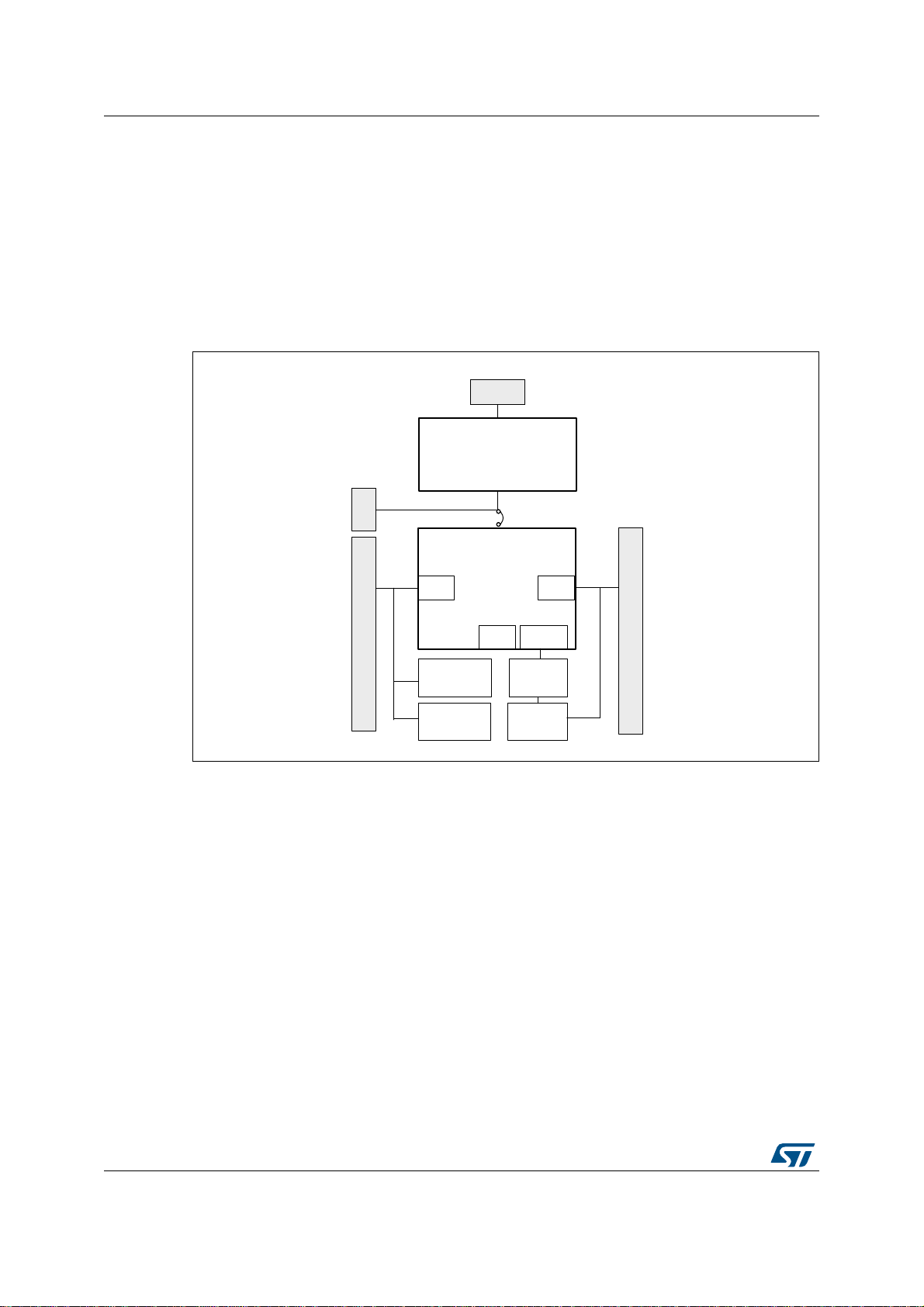
4 Hardware and layout
The 32L100CDISCOVERY is designed around the STM32L100RCT6 microcontroller in a
64-pin LQFP package.
Figure 2 illustrates the connections between the STM32L100RCT6 and its peripherals (ST-
LINK/V2, push button, LEDs and connectors) .
Figure 3 and Figure 4 help you to locate these features on the 32L100CDISCOVERY.
Figure 2. Hardware block diagram
8/30 DocID025091 Rev 1
Page 9
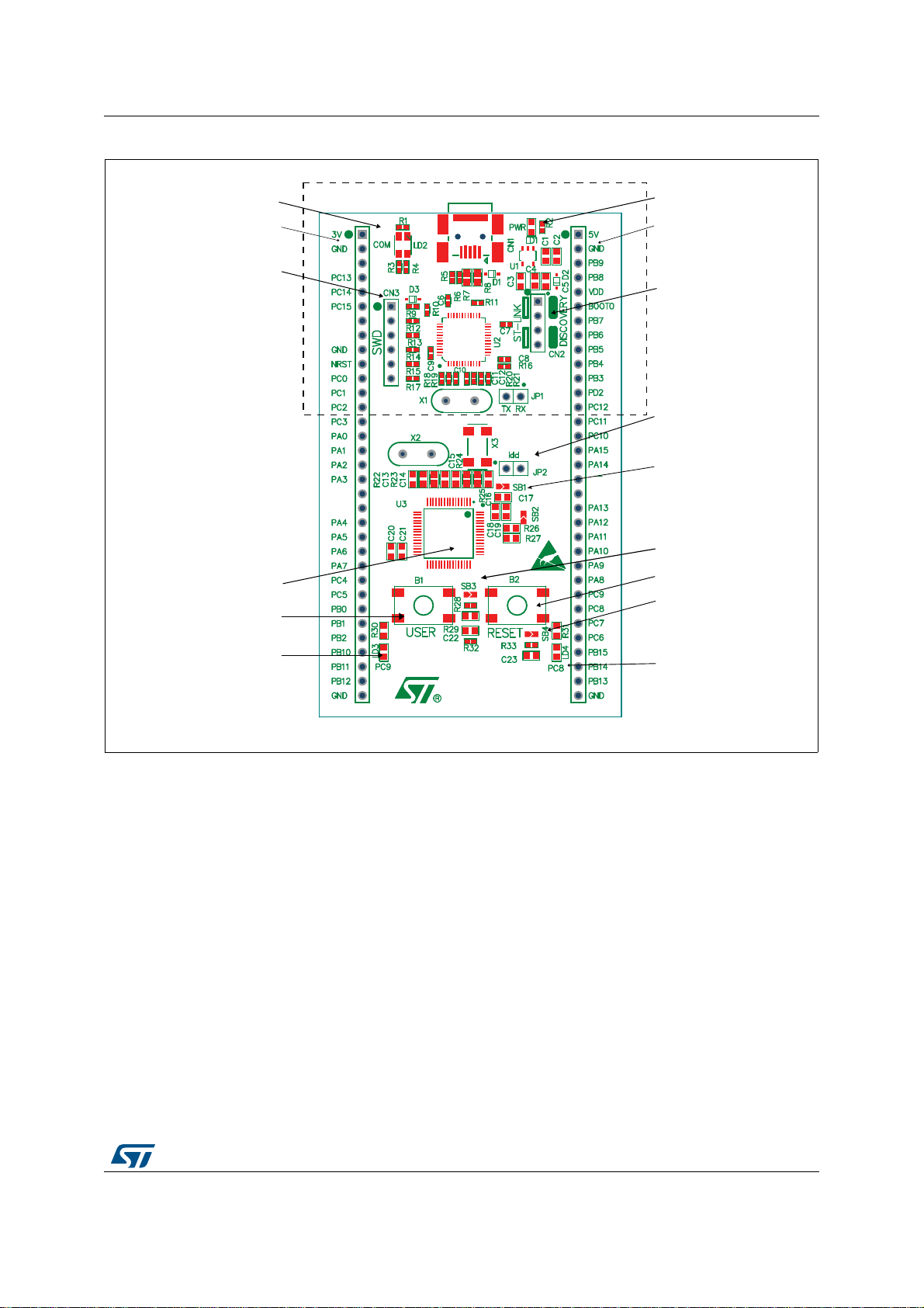
UM1656 Hardware and layout
MS32777V1
(red/green LED) LD2
COM
CN3
SWD connector
IDD measurement
ST-LINK/V2
B1 user button
B2 reset button
LD1 (red LED)
PWR
CN2
ST-LINK/DISCOVERY
selector
(green LED) LD3
LD4 (blue LED)
STM32L100RCT6
JP2
5V power supply
input/output
3V power supply
su
input/output
SB1 (VBAT)
SB3 (B1-USER)
SB4 (B2-RESET)
VLCD
GND
VDD
VDD
GND
MB1108 rev B
STM32L100C-DISCO
PH0
PH1
www.st.com/stm32l1-discovery
Figure 3. Top layout
1. Pin 1 of CN2, CN3, P1 and P2 connectors are identified by a square.
DocID025091 Rev 1 9/30
29
Page 10

Hardware and layout UM1656
SB6, SB8, SB10, SB12
MS30025V1
SB5, SB7, SB9, SB11
(RESERVED)
(DEFAULT)
SB20, SB21 (X3 crystal)
SB14, SB15 (RX, TX)
SB19 (NRST)
SB16, SB17 (X2 crystal)
SB13 (STM_RST)
SB22 (T_SWO)
SB18 (MCO)
Figure 4. Bottom layout
10/30 DocID025091 Rev 1
Page 11

UM1656 Hardware and layout
-36
34-,2#4
+BYTESOF&LASHMEMORY
+BYTESOF2!-
,1&0XMM
4.1 STM32L100RCT6 microcontroller
The V alue Line STM32L100RCT6 incorpor ates the connectivity power of the universal serial
bus (USB) with the high-performance ARM Cortex™-M3 32-bit RISC core operating at a
32 MHz frequency, a memory protection unit (MPU), high-speed embedded memories
(256 Kbytes of Flash memory and 16 Kbytes of RAM) and an extensive range of enhanced
I/Os and peripherals connected to two APB buses.
The STM32L100RCT6 device offers one 12-bit ADC, two DACs, two ultra-low-power
comparators, six general-purpose 16-bit timers and two basic timers, which can be used as
time bases.
Moreover, the STM32L100RCT6 device contains standard and advanced communication
interfaces: two I2Cs, three SPIs, two I2S, three USARTs and a USB.
It also includes a real-time clock and a set of backup registers that remain powered in
Standby mode.
Finally , the inte grated LCD contr oller has a built-in L CD voltag e generato r that allows you to
drive up to 8 multiplexed LCDs with contrast independent of the supply voltage.
The ultra-low-power STM32L100RCT6 operates from a 1.8 to 3.6 V power supply with
BOR. It is available in the -40 to +85 °C temperature range. A comprehensive set of powersaving modes allows the design of low-power applications.
Figure 5. STM32L100RCT6 package
DocID025091 Rev 1 11/30
29
Page 12

Hardware and layout UM1656
EXT. IT
WKU P
WIn WATCH DOG
12bit ADC
JTAG & SW
20 AF
NJTRST
JTDI
JTCK/SWCLK
JTMS/SWDAT
JTDO
As AF
NRST
V
DD
= 1.8 V to 3.6 V
V
SS
51 AF
USB 2.0 FS device
USB_DP
SRAM 16K
2x(8x16bi t)
f
MAX
:32 MHz
SCL,SDA,SMBus,PMBus
as AF
GP DMA 7 channels
XTAL OSC
1-24 MHz
AHPBCLK
APBPCLK
HCLK
FCLK
EEPROM 64 bit
VOLT. REG.
V
DDC ORE
POWER
Backup interface
Bu sMatrix 5M/5S
Interface
Ibu s
Dbus
obl
EE²
USB SRAM 512B
USART1
USART2
SPI2/I2S
5 x 32-Bit
backup
reg.
SCL,SDA as AF
I2C1
RX,TX,CTS,RTS,
SmartCard as AF
Standby
WDG32K
V
DDA
/
V
SSA
RX,TX,CTS,
RTS,SmartCard
as AF
NVIC
SPI1
MOSI,MISO,
SCK,NSS
as AF
IF
interface
PVD
BOR
Int
RTC V2
AWU
Sys tem
PA[15:0]
PB[15:0]
PC[15:0]
PD[15:0]
LCD 8x28 (4x32)
SEGx
COMx
12bit DAC1
FIFI
IF
DAC_OUT1 as AF
DAC_OUT2 as AF
MPU
Vref
GP Comp
BOR / Bgap
C OM Px_ IN x
PU / PD
PDR
PDR
TIMER6
1 Channel
General purpose
timers
256 KB
PROGRAM
4 KB DATA
8 KB BOOT
LCDBooster
V
LCD
PH [2:0]
RCLSI
MOSI,MISO,SCK,NSS,
WS,CK,MCK,SD as AF
2x( 8x16bit)
Supply
monitoring
@V
DDA
Supply monitoring
MS32904V1
APB2: f
MAX
= 32MHz
PLL &
Clock
Mgmt
AHB/
APB2
AHB/
APB1
GPIO PORTC
GPIO PORTD
GPIO PORTH
APB1: f
MAX
= 32MHz
@V
DDA
@V
DDA
@V
DD
@V
DD
@V
DD
@V
DDA
@V
DDA
TIMER7
TIMER2
TIMER3
TIMER4
V
LCD
= 2.5 V to 3.6 V
OSC32_IN
OSC32_OUT
RTC_OUT
OSC_IN
OSC_OUT
TAMPER
4 Channels
4 Channels
4 Channels
M3 CPU
GPIO PORTA
GPIO PORTB
AHB: f
MAX
= 32MHz
GP DMA2 5 channels
MOSI,MISO,SCK,NSS,
WS,CK,MCK,SD as AF
RX,TX,CTS,RTS,
SmartCard as AF
RCMSI
RCHSI
1 Channel
2 Channels
XTAL 32kHz
12bit DAC2
USB_DM
USART3
SPI3/I2S
I2C2
TIMER9
TIMER10
TIMER11
Figure 6. STM32L100RCT6 block diagram
12/30 DocID025091 Rev 1
Page 13

UM1656 Hardware and layout
-36
(ARDWAREREQUIREMENTS
53"CABLETYPE!TOMINI"
COMPUTERWITH7INDOWS806ISTAOR
$EVELOPMENTTOOLCHAIN
!LTIUM4!3+).'684OOLSET
!TOLLIC4RUE345$)/
)!2%7!2+EIL-$+!2-
4.2 Embedded ST-LINK/V2
The ST-LINK/V2 programming and debugging tool is integrated on the
32L100CDISCOVERY. The embedded ST-LINK/V2 can be used in 2 different ways
according to the jumper states (see Table 2):
• Program/debug the MCU on board,
• Program/debug an MCU in an external application board using a cable connected to
SWD connector CN3.
The embedded ST-LINK/V2 supports only SWD for STM32 devices. For information about
debugging and programming features refer to user manual UM1075 (ST-LINK/V2 in-circuit
debugger/programmer for STM8 and STM32) which describes in detail all the ST-LINK/V2
features.
Figure 7. Typical configuration
T able 2. Jumper states
Jumper state Description
Both CN2 jumpers ON ST-LINK/V2 functions enabled for on board programming (default)
Both CN2 jumpers OFF
ST-LINK/V2 functions enabled for application through external CN3
connector (SWD supported)
DocID025091 Rev 1 13/30
29
Page 14

Hardware and layout UM1656
-36
CN2 jumpers ON
CN3
SWD connector
4.2.1 Using ST-LINK/V2 to program/debug the STM32L100 Value Line on board
To program the STM32L100 Value Line microcontroller on board, simply plug in the two
jumpers on CN2, as shown in Figure 8 in red, but do not use the CN3 connector as that
could disturb communication with the STM32L100RCT6 of the 32L100CDISCOVERY.
Figure 8. 32L100CDISCOVERY connections
14/30 DocID025091 Rev 1
Page 15

UM1656 Hardware and layout
-36
CN2 jumpers OFF
CN3
SWD connector
4.2.2 Using ST-LINK/V2 to program/debug an external STM32 application
It is very easy to use the ST-LINK/V2 to program the STM32 on an external application.
Simply remove the 2 jumpers from CN2 as shown in Figure 9, and connect your application
to the CN3 debug connector according to Table 3.
Note: SB19 and SB22 must be OFF if you use CN3 pin 5 in your external application.
Pin CN3 Designation
1 VDD_TARGET VDD from application
2 SWCLK SWD clock
3 GND Ground
4 SWDIO SWD data input/output
5 NRST RESET of target MCU
6 SWO Reserved
Table 3. Debug connector CN3 (SWD)
Figure 9. ST-LINK connections
DocID025091 Rev 1 15/30
29
Page 16

Hardware and layout UM1656
4.3 Power supply and power selection
The power supply is provided either by the host PC through the USB cable, or by an
external 5V power supply.
The D1 and D2 diodes protect the 5V and 3V pins from external power supplies:
• 5V and 3V can be used as output power supplies when another application board is
connected to pins P1 and P2.
In this case, the 5V and 3V pins deliver a 5V or 3V power supply and power
consumption must be lower than 100 mA.
• 5V can also be used as input power su pplies e.g. when the USB connector is not
connected to the PC.
In this case, the 32L100CDISCOVERY board must be powered by a power supply un it
or by auxiliary equipment complying with standard EN-60950-1: 2006+A11/2009, and
must be Safety Extra Low Voltage (SELV) with limited power capability.
4.4 LEDs
• LD1 PWR: Red LED indicates that the board is powered.
• LD2 COM: Tricolor LED (COM) advises on the communication status as follows:
– Slow blinking Red LED/Off: At power on before USB initialization
– Fast blinking Red LED/Off: After the first correct communication between PC and
STLINK/V2 (enumeration)
– Red LED On: When initialization between PC and ST-LINK/V2 is successfully
finished
– Green LED On: After successful target communication initialization
– Blinking Red/Green LED: During communication with target
– Red LED On: Communication finished and OK
– Orange LED On: Communication failure
• User LD3: Green user LED connected to the I/O PC9 of the STM32L100RCT6.
• User LD4: Blue user LED connected to the I/O PC8 of the STM32L100RCT6.
4.5 Push buttons
• B1 USER: User push button co nnected to the I/O PA0 of the STM32L100RCT6.
• B2 RESET: Push button used to RESET the STM32L100RCT6.
4.6 JP2 (IDD)
Jumper JP2, labeled IDD, allows the consumption of STM32L100RCT6 to be measured by
removing the jumper and connecting an ammeter.
• Jumper on: STM32L100RCT6 is powered (default).
• Jumper off: an ammeter must be connected to measure the STM32L100RCT6 current,
(if there is no ammeter, the STM32L100RCT6 is not powered).
16/30 DocID025091 Rev 1
Page 17

UM1656 Hardware and layout
4.7 Oscillator clock (OSC)
4.7.1 OSC clock supply
PH0 and PH1 can be used as GPIO or as HSE oscillator. By default these I/Os are
configured as GPIO, so SB16 and SB17 are closed, SB18 is open and R22, R23, C13 and
C14 are not populated.
An external HSE clock can be provided to the MCU in three ways:
• MCO from ST-LINK. From MCO of the STM32F103. This frequency cannot be
changed, it is fixed at 8 MHz and connected to PH0-OSC_IN of the STM32L100RCT6.
Configuration needed:
– SB16, SB18 CLOSED
– R22, R23 removed
– SB17 OPEN
• Oscillator onboard. From X2 crystal (not provided). For typical frequencies and its
capacitors and resistors, please refer to the STM32L100RCT6 Datasheet.
Configuration needed:
– SB16, SB17 SB18 OPEN
– R22, R23, C13, C14 soldered
• Oscillator from external PH0. From external oscillator through pin 7 of the P1
connector. Configuration needed:
– SB16, SB17 CLOSED
– SB18 OPEN
– R22 and R23 removed
4.7.2 OSC 32 KHz clock supply
PC14 and PC15 can be used as GPIO or as LSE oscillator. By default these I/Os are
configured as GPIO, so SB20 & SB21 are closed and X3, R24, R25 are not populated.
An external LSE clock can be provided to the MCU in two ways:
• Oscillator onboard. From X3 crystal (not provided). Configuration needed:
– SB20, SB21 OPEN
– C15, C16, R24 and R25 soldered.
• Oscillator from external PC14. From external oscillator trough the pin 5 of P1
connector. Configuration needed:
– SB20, SB21 CLOSED
– R24 and R25 removed
DocID025091 Rev 1 17/30
29
Page 18

Hardware and layout UM1656
4.8 Solder bridges
SB16,17
(X2 crystal)
Bridge State
OFF
(2)
ON PH0, PH1 are connected to P1 (R22, R23 and SB18 must not be fitted).
Table 4. Solder bridge settings
(1)
Description
X2, C13, C14, R22 and R23 provide a clock. PH0, PH1 are disconnected
from P1.
SB6,8,10,12 (Default) ON Reserved, do not modify.
SB5,7,9,11 (Reserved) OFF Reserved, do not modify.
SB20,21
(X3 crystal)
SB4
(B2-RESET)
SB3
(B1-USER)
SB1
(VBAT powered from VDD)
OFF
ON PC14, PC15 are only connected to P1 (R24, R25 must not be fitted).
ON
OFF
ON B1 push button is connected to PA0.
OFF B1 push button is not connected to PA0.
ON VBAT is permanently powered from VDD.
OFF VBAT is not powered from VDD but pin3 of P1.
X3, C15, C16, R24 and R25 deliver a 32 KHz clock. PC14, PC15 are not
connected to P1.
B2 push button is connected to the NRST pin of the STM32L100RCT6
MCU.
B2 push button is not connected the NRST pin of the STM32L100RCT6
MCU.
SB14,15
(RX,TX)
SB19
(NRST)
SB22
(T_SWO)
SB13
(STM_RST)
SB2
(BOOT0)
SB18
(2)
(MCO)
1. Default SBx state is shown in bold.
2. OSC_IN clock comes from MCO if SB18 is ON and SB16,17 are OFF
and comes from X2 if SB18 is OFF and SB16,17 are ON.
OFF Reserved, do not modify.
ON Reserved, do not modify.
ON
OFF
NRST signal of the CN3 connector is connected to the NRST pin of the
STM32L100RCT6 MCU.
NRST signal of the CN3 connector is not connected to the NRST pin of the
STM32L100RCT6 MCU.
ON SWO signal of the CN3 connector is connected to PB3.
OFF SWO signal is not connected.
OFF No incidence on STM32F103C8T6 (ST-LINK/V2) NRST signal.
ON STM32F103C8T6 (ST-LINK/V2) NRST signal is connected to GND.
ON
OFF
BOOT0 signal of the STM32L100RCT6 MCU is held low through a
510 Ohm pull-down resistor.
BOOT0 signal of the STM32L100RCT6 MCU can be set high through a
10 K Ω pull-up resistor R27 to solder.
ON Provides the 8 MHz for OSC_IN from MCO of STM32L100RCT6.
OFF See SB16, SB17 description.
18/30 DocID025091 Rev 1
Page 19

UM1656 Hardware and layout
4.9 Extension connectors
The male headers P1 and P2 can connect the 32L100CDISCOVERY to a standard
prototyping/wrapping board. STM32L100RCT6 GPI/Os are available on these connectors.
P1 and P2 can also be probed by an oscilloscope, logical analyzer or voltmeter.
Table 5. MCU pin description versus board function
MCU pin Board function
Main
function
BOOT0 BOOT0 60 6
NRST NRST 7
WKUP1/RTC_TAMP2/
PA0
PA1
PA2
PA3
PA4
PA5
PA6
TIM2_CH1_ETR/
USART2_CTS/ADC_IN0/
COMP1_INP
TIM2_CH2/USART2_RTS/
LCD_SEG0/ADC_IN1/
COMP1_INP/OPAMP1_VINP
TIM2_CH3/TIM9_CH1/
USART2_TX/LCD_SEG1/
ADC_IN2/COMP1_INP/
OPAMP1_VINM
TIM2_CH4/TIM9_CH2/
USART2_RX/LCD_SEG2/
ADC_IN3/COMP1_INP/
OPAMP1_VOUT
SPI1_NSS/SPI3_NSS/
I2S3_WS/USART2_CK/
ADC_IN4/DAC_OUT1/
COMP1_INP
TIM2_CH1_ETR/SPI1_SCK
/ADC_IN5/DAC_OUT2/
COMP1_INP
TIM3_CH1/TIM10_CH1/
SPI1_MISO/LCD_SEG3/
ADC_IN6/COMP1_INP/
OPAMP2_VINP
Alternate
functions
14
15
16
17
20
21
22
LQFP64
RESET
USER
LED
Push button
NRST
SWD
OSC
Free I/O
Power supply
P1
CN3
510
15
16
17
18
21
22
23
P2
DocID025091 Rev 1 19/30
29
Page 20

Hardware and layout UM1656
Table 5. MCU pin description versus board function (continued)
MCU pin Board function
Main
function
TIM3_CH2/TIM11_CH1/
PA7
PA8
PA9 USART1_TX/LCD_COM1 42 24
PA10 USART1_RX/LCD_COM2 43
PA11
PA12
PA13 JTMS-SWDAT 46
SPI1_MOSI/LCD_SEG4/
ADC_IN7/COMP1_INP
/OPAMP2_VINM
USART1_CK/MCO/
LCD_COM0
USART1_CTS/USB_DM/
SPI1_MISO
USART1_RTS/USB_DP/
SPI1_MOSI
Alternate
functions
LQFP64
23
41
44 22
45
LED
Push button
SWD
SWDIO
SWCLK
OSC
Free I/O
Power supply
P1
CN3
24
25
23
21
420
P2
PA14 JTCK-SWCLK 49
TIM2_CH1_ETR/SPI1_NSS
PA15
PB0
PB1
PB2/BO
OT1
PB3
20/30 DocID025091 Rev 1
/SPI3_NSS/I2S3_WS/
LCD_SEG17
TIM3_CH3/LCD_SEG5/
ADC_IN8/COMP1_INP/
VREF_OUT/
OPAMP2_VOUT
TIM3_CH4/LCD_SEG6/
ADC_IN9/COMP1_INP/
VREF_OUT
COMP1_INP 28 29
TIM2_CH2/SPI1_SCK/
SPI3_SCK/I2S3_CK/
LCD_SEG7/COMP2_INM
50
26
27
55
217
16
27
28
SWO
611
Page 21

UM1656 Hardware and layout
Table 5. MCU pin description versus board function (continued)
MCU pin Board function
Main
function
PB4
PB5
PB6
PB7
PB8
PB9
PB10
PB11
PB12
PB13
Alternate
functions
TIM3_CH1/SPI1_MISO/
SPI3_MISO/LCD_SEG8/
COMP2_INP
TIM3_CH2/I2C1_SMBA/
SPI1_MOSI/SPI3_MOSI
/I2S3_SD/LCD_SEG9/
COMP2_INP
TIM4_CH1/I2C1_SCL/
USART1_TX/COMP2_INP
TIM4_CH2/I2C1_SDA/
USART1_RX/PVD_IN/
COMP2_INP
TIM4_CH3/TIM10_CH1
/I2C1_SCL/LCD_SEG16
TIM4_CH4/TIM11_CH1
/I2C1_SDA/LCD_COM3
TIM2_CH3/I2C2_SCL/
USART3_TX/LCD_SEG10
TIM2_CH4/I2C2_SDA/
USART3_RX/LCD_SEG11
TIM10_CH1/I2C2_SMBA/
SPI2_NSS/I2S2_WS/
USART3_CK/LCD_SEG12/
ADC_IN18/COMP1_INP
TIM9_CH1/SPI2_SCK/
I2S2_CK/USART3_CTS/
LCD_SEG13/ADC_IN19
/COMP1_INP
LQFP64
Push button
LED
SWD
OSC
Free I/O
Power supply
CN3
P1
56 10
57
58
59
61
62
29
30
33
34
30
31
32
32
P2
9
8
7
4
3
PB14
PB15
TIM9_CH2/SPI2_MISO/
USART3_RTS/LCD_SEG14
/ADC_IN20/COMP1_INP
TIM11_CH1/SPI2_MOSI
/I2S2_SD/LCD_SEG15/
ADC_IN21/COMP1_INP/
RTC_REFIN
DocID025091 Rev 1 21/30
35
36
31
30
29
Page 22

Hardware and layout UM1656
Table 5. MCU pin description versus board function (continued)
MCU pin Board function
Main
function
PC0
PC1
PC2
PC3
PC4
PC5
PC6
PC7
PC8 TIM3_CH3/LCD_SEG26 39
LCD_SEG18/ADC_IN10/
COMP1_INP
LCD_SEG19/ADC_IN11/
COMP1_INP
LCD_SEG20/ADC_IN12/
COMP1_INP
LCD_SEG21/ADC_IN13/
COMP1_INP
LCD_SEG22/ADC_IN14/
COMP1_INP
LCD_SEG23/ADC_IN15/
COMP1_INP
TIM3_CH1/I2S2_MCK
/LCD_SEG24
TIM3_CH2/I2S3_MCK/
LCD_SEG25
Alternate
functions
10
11
24
25
37
38
LQFP64
8 11
9
LED
Push button
BLUE
GREEN
SWD
OSC
Free I/O
CN3
Power supply
12
13
14
25
26
P1
P2
29
28
27
PC9 TIM3_CH4/LCD_SEG27 40
SPI3_SCK/I2S3_CK/
PC10
PC11
PC12
PC13
22/30 DocID025091 Rev 1
USART3_TX/LCD_SEG28/
LCD_SEG40/LCD_COM4
SPI3_MISO/USART3_RX/
LCD_SEG29/LCD_SEG41/
LCD_COM5
SPI3_MOSI/I2S3_SD/
USART3_CK/LCD_SEG30/
LCD_SEG42/LCD_COM6
WKUP2/RTC_TAMP1/
RTC_TS/RTC_OUT
51
52
53
2
26
15
14
13
4
Page 23

UM1656 Hardware and layout
Table 5. MCU pin description versus board function (continued)
MCU pin Board function
Main
function
Alternate
functions
PC14OSC32_INOSC32_IN 3
PC15OSC32_
OSC32_OUT 4
OUT
PD2
PH0OSC_IN
TIM3_ETR/LCD_SEG31/
LCD_SEG43/LCD_COM7
OSC_IN 5
PH1OSC_
OSC_OUT 6
OUT
54
LQFP64
Push button
LED
SWD
OSC
Free I/O
OSC32_IN
OSC32_OUT
OSC_IN
OSC_OUT
P1
CN3
Power supply
5
6
7
8
P2
12
VSS VSS 18 19
VDD VDD 19
20
VSS_2 VSS 47
VDD_2 VDD 48
VLCD VLCD 1 3
VDD_3 64
VDD_1 32
VDDA 13
VSS_3 63
VSS_1 31
VSSA 12
5V 1
3V 1
VDD
DocID025091 Rev 1 23/30
19
18
5
29
Page 24

Hardware and layout UM1656
Table 5. MCU pin description versus board function (continued)
MCU pin Board function
Main
function
Alternate
functions
LQFP64
Push button
LED
SWD
GND
OSC
Free I/O
Power supply
GND
GND
GND
GND
CN3
3
P1
P2
22
9
33 33
24/30 DocID025091 Rev 1
Page 25

UM1656 Mechanical drawing
5 Mechanical drawing
Figure 10. 32L100CDISCOVERY mechanical drawing
VLCD
PH0
PH1
GND
VDD
www.st.com/stm32l1-discovery
VDD
GND
MB1108 rev B
STM32L100C-DISCO
-36
DocID025091 Rev 1 25/30
29
Page 26

26/30 DocID025091 Rev 1
-36
STMicroelectronics
Title:
Number: Rev: Sheet of
B.1(PCB.SCH)
Date:
6/3/2013
MB1108 1 3
STM32L100 Discovery
PA13
PA14
NRST
PB3
MCO
PA10
PA9
U_ST_LINK
ST_LINK_V2.SCHDOC
PA13
PA14 TCK /SWCLK
TMS/SWDIO
MCO
NRST
PB3 T_SWO
T_NRST
MCO
PA0
PA1
PA2
PA3
PA4
PA5
PA6
PA7
PA8
PA9
PA10
PA1 1
PA12
PA13
PA14
PA15
PB0
PB1
PB2
PB3
PB4
PB5
PB6
PB7
PB8
PB9
PB10
PB1 1
PB12
PB13
PB14
PB15
PC0
PC1
PC2
PC3
PC4
PC5
PC6
PC7
PC8
PC9
PC10
PC1 1
PC12
PC13
PC14
PC15
PH0
BOOT0
NRST
PD2
PA4
PA5
PA0
PA3
PA2
PA1
PB14
PB15
PB2
PB12
PB13
PC0
PC1
PC2
PC3
NRST
PH1
PH0
PC15
PC14
PC13
VLCD
PB10
PB1 1
PC7
PC8
PC9
PA8
PA9
PA10
PA1 1
PA12
PA14
BOOT0
PB8
PB9
PA13
PA15
PC10
PC1 1
PC12
PD2
PB3
PB4
PB5
PB6
PB7
PC6
VDD
3V
5V
VL CD
PH1
PA10
PA9
1
2
3
4
5
6
7
8
9
10
11
12
13
14
15
16
17
18
19
20
21
22
23
24
25
26
27
28
29
30
31
32
33
P1
Header 33
1
2
3
4
5
6
7
8
9
10
11
12
13
14
15
16
17
18
19
20
21
22
23
24
25
26
27
28
29
30
31
32
33
P2
Header 33
PA6
PA7
PC4
PC5
PB0
PB1
VDD
VDD
BOOT0
PA14
PA15
PC10
PC1 1
PC12
PD2
PB4
PB5
PB6
PB7
PB8
PB9
PB12
PB13
PB14
PB15
PC6
PC7
PC8
PC9
PA3
PA4
PA5
PA6
PA7
PC4
PC5
PB0
PB1
PB2
PB10
PB1 1
NRST
MCO
PC14
PC15
PC13
PA0
PA1
PA2
PC0
PC1
PC2
PC3
PB3
VL CD
PA8
PA9
PA11
PA13
PA10
PA12
PH0
PH1
U_STM32L100RCT6
STM32L100RCT6.SchDoc
6 Electrical schematics
Electrical schematics UM1656
Figure 11. 32L100CDISCOVERY
RevB.1 --> increased PADs of P1 & P2 for easy PCB manufacturing
RevA.1 --> PCB label MB1108 Rev. A
Page 27

Figure 12. ST-LINK/V2 (SWD only)
UM1656 Electrical schematics
DocID025091 Rev 1 27/30
Board Ident: PC13=0
Not Fitted
C11
20pF
3V
R16
100K
C8
100nF
SB13
STM32L100C USART1_RX
PA10
STM32L100C USART1_TX
PA9
USB
U5V
CN1
1
VCC
2
D-
3
D+
4
ID
5
GND
0
SHELL
5075BMR-05-SM
X1
1 2
8MHz
3V
Close to JP
Not Fitted
R6 1K5
R8 0
R7 0
R5 100K
R18 10K
R19 10K
C10
20pF
R20 4K7
R21 4K7
D1
BAT60JFILM
OS C_ IN
OSC_O UT
STM_RST
SB14
SB15
USB_ DM
USB_DP
AIN_1
STLI N K_ TX
JP1TXRX
EXT_5V
10
11
12
5V
3V
3V
1
VBAT
2
PC13
3
PC14
4
PC15
5
OSCIN
6
OSCOUT
7
NRST
8
VSSA
9
VDDA
PA0
PA1
PA2
STLINK_RX
Not Fitted
TCK /SWCLK
TMS/SWDIO
T_NRST
R13
100K
IM
IM_IN
SW
SWIM_RST_ IN
SW I M _RST
STM_ JTCK
SW
SWIM_IN
45
41
43
46
48
47
PB9
VSS_3
VDD_3
PA3
PA4
PA5
13
14
15
T_JTCK
39
42
38
40
44
PB8
BOOT0
PA7
PA6
17
16
T_JTDI
T_JTDO
3V
37
PB6
PB5
PB7
/SWCLK
PB3/ JT DO
PA15 /JTDI
VDD_2
PB4/ JN T RST
JTCK
VSS_2
JTMS/SWDIO
/BOOT1
PB0
PB2
PB10
PB11
VSS_1
VDD_1
PB1
20
18
21
22
23
24
19
IN
C6
100nF
3V
SWIM_
SWI M
C7
100nF
T_JRST
T_NRST
PA12
PA11
PA10
PA9
PA8
PB15
PB14
PB13
PB12
C12
100nFC9100nF
U2
STM32F 103C8T6
36
35
34
STM_JTMS
33
USB_DP
32
USB_ DM
31
T_SWO
30
LED _S TL I NK
29
28
27
T_JTMS
26
T_JTCK
25
3V
T_SW DIO_ IN
R34
100
R11
100
R2
1K
LD1
RED
R9
10K
SWD
CN3
1
2
3
4
5
6
Header 6
RC Must be very close to STM32F103 pin 29
MCO
C24
20pF
MCO
Not Fitted
Idd
VDD3V
JP2
D3
BAT60JFILM
R12
R14
R15
R17
R10
22
22
22
22
Not Fitted
100
T_JTCK
T_JTMS
T_NRST
T_SWO
5V
AIN_1
3
C1
1uF_X5R_0603
C2
100nF
U1
Vin Vout
INH
LD3985M33R
T_SWO
SB22
123
R4
100
R3
100
RESE R V ED
4
LD2
Red
2 1
3 4
_Green
LD_BICOLOR_CMS
DEFAULT
SB6 SB5
SB8 SB7
SB10 SB9
SB12 SB11
CN2
Jumpers ON --> DISCOVERY Selected
Jumpesr OFF --> ST-LINK DISCOVERY Selected
COM
LED STLINK
PWR
51
C3
10nF_X7R_0603
C4
1uF_X5R_0603
C5
100nF
GND
BYPASS
2
4
SB19
STM_JTCK
STM_JTMS
D2
BAT60JFILM
3V
R1
0
OUT_3V
PA14
PA13
NRST
PB3
SWCLK
SWDIO
3V
3V
SWD
STMicroelectronics
Title:
STM32L100 Discovery ST-LINK/V2 (SWD only)
Number: Rev: Sheet of
MB1108 2 3
B.1(PCB.SCH)
Date:
6/3/2013
-36
Page 28

-36
STMicroelectronics
Title:
Number: Rev: Sheet of
B.1(PCB.SCH)
Date:
6/3/2013
MB1108 3 3
STM32L100 Discovery MCU
C21
100nF
C19
100nF
VDD
C20
100nF
VDD
PA0
PA1
PA2
PA3
PA4
PA5
PA6
PA7
PA8
PA9
PA1 0
PA1 1
PA1 2
PA1 3
PA14
PA15
PB0
PB1
PB2
PB3
PB4
PB5
PB6
PB7
PB8
PB9
PB10
PB1 1
PB12
PB13
PB14
PB15
PC0
PC1
PC2
PC3
PC4
PC5
PC6
PC7
PC8
PC9
PC10
PC1 1
PC12
PC13
PC14
PC15
PH0
PH1
PD2
C15
6.8pF
C16
6.8pF
R24
0
R25
0
C13
20pF
C14
20pF
R22
390
VDD
R27
10K
VDD
NRST
BOOT0
1 2
X2
8MHz
41
32
X3
MC306-G-06Q-32.768 (JFVNY)
R26
510
SB2
BOOT0
PA14
PA15
PC10
PC1 1
PC12
PD2
PB3
PB4
PB5
PB6
PB7
PB8
PB9
PB12
PB13
PB14
PB15
PC6
PC7
PC8
PC9
PA8
PA9
PA1 0
PA1 1
PA1 2
PA1 3
PA3
PA4
PA5
PA6
PA7
PC4
PC5
PB0
PB1
PB2
PB10
PB1 1
LD3
green
PC9
R30
330
LD4
blue
PC8
R31
660
C22
100nF
R29
220K
VDD
SB3
R28
330
R32
100
USER & WAKE-UP Button
PA0
Not Fitted
NRST
NRST
RESET Button
C23
100nF
R33
100K
VDD
SB4
Not Fitted
14
3 2
B2
SW- PU SH - CM S
1
4
3 2
B1
SW- PU SH - CM S
MCO
MCO
SB18
PC14
PC15
PH0
PH1
PC13
SB20
PA0
PA1
PA2
PC0
PC1
PC2
SB17
SB21
VDD
R23
0
SB16
C18
1uF
PC3
VDD
VL CD
C17
1uF
SB1
Close to XTAL & MCU
Close to STM32
Not Fitted
Not Fitted
VLCD
1
PC13 - TAMPER1 - WKUP22PC14 - OSC32_IN
3
PC15 - OSC32_OUT4PH0 - OSC_I N5PH1 - OSC_OUT
6
NRST
7
PC08PC1
9
PC210PC3
11
VSSA / VREF-12VDDA / VREF+13PA0 - TAM PER2 - WKUP114PA115PA2
16
PA3
17
VSS_4
18
VDD_4
19
PA4
20
PA5
21
PA6
22
PA7
23
PC4
24
PC5
25
PB0
26
PB1
27
PB2 or NPOR (1.8V mode)
28
PB10
29
PB11
30
VSS_1
31
VDD_1
32
PB1233PB13
34
PB14
35
PB15
36
PC6
37
PC738PC8
39
PC9
40
PA8
41
PA9
42
PA1 043PA1 1
44
PA1 245PA1 3
46
VSS_2
47
VDD_2
48
PA14
49
PA15
50
PC10
51
PC11
52
PC12
53
PD2
54
PB3
55
PB4
56
PB5
57
PB6
58
PB7
59
BOOT0
60
PB8
61
PB9
62
VSS_3
63
VDD_3
64
U3
STM32L 100RCT6
VDD
VDD
28/30 DocID025091 Rev 1
Figure 13. MCU
Electrical schematics UM1656
Page 29

UM1656 Revision history
7 Revision history
Table 6. Document revision history
Date Revision Changes
12-Aug-2013 1 Initial release.
DocID025091 Rev 1 29/30
29
Page 30

UM1656
Please Read Carefully:
Information in this document is provided solely in connection with ST products. STMicroelectronics NV and its subsidiaries (“ST”) reserve the
right to make changes, corrections, modifications or improvements, to this document, and the products and services described herein at any
time, without notice.
All ST products are sold pursuant to ST’s terms and conditions of sale.
Purchasers are solely res ponsibl e fo r the c hoic e, sele cti on an d use o f the S T prod ucts and s ervice s des crib ed he rein , and ST assumes n o
liability whatsoever relati ng to the choice, selection or use of the ST products and services described herein.
No license, express or implied, by estoppel or otherwise, to any intellectual property rights is granted under this document. If any part of this
document refers to any third part y p ro duct s or se rvic es it sh al l n ot be dee med a li cens e gr an t by ST fo r t he use of su ch thi r d party products
or services, or any intellectua l property c ontained the rein or consi dered as a warr anty coverin g the use in any manner whats oever of such
third party products or services or any intellectual property contained therein.
UNLESS OTHERWISE SET FORTH IN ST’S TERMS AND CONDITIONS OF SALE ST DISCLAIMS ANY EXPRESS OR IMPLIED
WARRANTY WITH RESPECT TO THE USE AND/OR SALE OF ST PRODUCTS INCLUDING WITHOUT LIMITATION IMPLIED
WARRANTIES OF MERCHANTABILITY, FITNESS FOR A PARTICUL AR PURPOS E (AND THEIR E QUIVALENTS UNDER THE LAWS
OF ANY JURISDICTION), OR INFRINGEMENT OF ANY PATENT, COPYRIGHT OR OTHER INTELLECTUAL PROPERTY RIGHT.
ST PRODUCTS ARE NOT AUTHORIZED FOR USE IN WEAPONS. NOR ARE ST PRODUCTS DESIGNED OR AUTHORIZED FOR USE
IN: (A) SAFETY CRITICAL APPLICATIONS SUCH AS LIFE SUPPORTING, ACTIVE IMPLANTED DEVICES OR SYSTEMS WITH
PRODUCT FUNCTIONAL SAFETY REQUIREMENTS; (B) AERONAUTIC APPLICATIONS; (C) AUTOMOTIVE APPLICATIONS OR
ENVIRONMENTS, AND/OR (D) AEROSPACE APPLICATIONS OR ENVIRONMENTS. WHERE ST PRODUCTS ARE NOT DESIGNED
FOR SUCH USE, THE PURCHASER SHALL USE PRODUCTS AT PURCHASER’S SOLE RISK, EVEN IF ST HAS BEEN INFORMED IN
WRITING OF SUCH USAGE, UNLESS A PRODUCT IS EXPRESSLY DESIGNATED BY ST AS BEING INTENDED FOR “AUTOMOTIVE,
AUTOMOTIVE SAFETY OR MEDICAL” INDUSTRY DOMAINS ACCORDING TO ST PRODUCT DESIGN SPECIFICATIONS.
PRODUCTS FORMALLY ESCC, QML OR JAN QUALIFIED ARE DEEMED SUITABLE FOR USE IN AEROSPACE BY THE
CORRESPONDING GOVERNMENTAL AGENCY.
Resale of ST products with provisions different from the statements and/or technical features set forth in this document shall immediately void
any warranty granted by ST for the ST product or service described herein and shall not create or extend in any manner whatsoever, any
liability of ST.
ST and the ST logo are trademarks or registered trademarks of ST in various countries.
Information in this document supersedes and replaces all information previously supplied.
The ST logo is a registered trademark of STMicroelectronics. All other names are the property of their respective owners.
© 2013 STMicroelectronics - All rights reserved
STMicroelectronics group of compan ie s
Australia - Belgium - Brazil - Canada - China - Czech Republic - Finland - France - Germany - Hong Kong - India - Israel - Italy - Japan -
Malaysia - Malta - Morocco - Philip pines - Singapore - Spain - Sweden - Switzerland - United Kingdom - United States of America
www.st.com
30/30 DocID025091 Rev 1
 Loading...