

2N7000
2N7002
N-CHANNEL 60V - 1.8Ω - 0.35A SOT23-3L - TO-92
STripFET™II MOSFET
Table 1: General Features
TYPE V
2N7000
2N7002
Q TYPICAL R
Q LOW Q
Q LOW THRESHOLD DRIVE
g
DSS
60 V
60 V
(on) = 1.8Ω @10V
DS
R
DS(on)
< 5 Ω (@ 10V)
< 5 Ω (@ 10V)
I
d
0.35 A
0.20 A
DESCRIPTION
This MOSFET is the second gene ration of STM icroelectronics unique “Single Feature Size™”
strip-based process. The resulting transistor
shows extremely high packing den sity for low onresistance, rugged a valanche character istics and
less critical alignment steps therefore a remarkable manufacturing repr odu ci bi lit y.
APPLICATIONS
Q HIGH SWITCHING APPLICATIONS
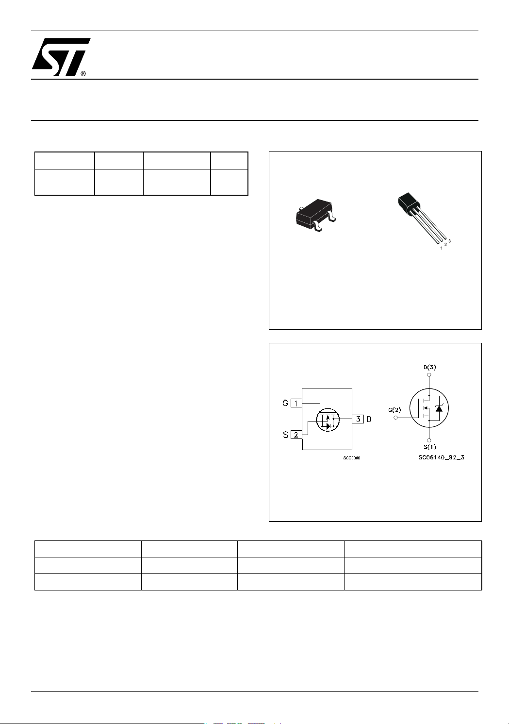
Figure 1: Package
3
2
1
SOT23-3L
TO-92
Figure 2: Internal Schematic Diagram
SOT23-3L TO-92
Table 2: Order Codes
SALES TYPE MARKING PACKAGE PACKAGING
2N7000 2N7000G TO-92 BULK
2N7002 ST2N SOT23-3L TAPE & REEL
Rev. 3
1/11April 2005
2N7000 - 2N7002
Table 3: Absolute Maximum ratings
Symbol Parameter Value Unit
TO-92 SOT23-3L
V
DS
V
DGR
V
GS
I
D
I
DM
P
TOT
() Pulse width limited by safe operating area
Table 4: Thermal Data
Rthj-amb Thermal Resistance Junction-ambient Max 125 357.1 (*) °C/W
T
J
T
stg
(#) When mounted on 1inch² FR-4, 2 Oz copper board.
Drain-source Voltage (VGS = 0)
Drain-gate Voltage (RGS = 20 kΩ)
60 V
60 V
Gate- source Voltage ± 18 V
Drain Current (continu ou s) at TC = 25°C
()
Drain Current (pulsed ) 1.4 1 A
Total Dissipation at TC = 25°C
0.35 0.20 A
10.35W
TO-92 SOT23-3L
Operating Junction Temperature
Storage Temperature
- 55 to 150 °C
ELECTRICAL CHARACTERISTICS (T
=25°C UNLESS OTHERWISE SPECIFIED)
CASE
Table 5: On/Off
Symbol Parameter Test Conditions Min. Typ. Max. Unit
V
(BR)DSS
I
DSS
I
GSS
V
GS(th)
R
DS(on)
Drain-source
Breakdown Voltage
Zero Gate Voltage
Drain Current (V
GS
= 0)
Gate-body Leakage
Current (V
DS
= 0)
Gate Threshold Voltage
Static Drain-source On
Resistance
ID = 250 µA, VGS = 0 60 V
V
= Max Rating
DS
VDS = Max Rating, TC = 125°C
V
= ± 18 V ±100 nA
GS
V
= VGS, ID = 250 µA
DS
VGS = 10 V, ID = 0.5 A
V
= 4.5 V, ID = 0.5 A
GS
12.1
1.8
2
1µA
10 µA
3V
5
5.3
Ω
Ω
2/11
2N7000 - 2N7002
ELECTRICAL CHARACTERISTICS (CONTINUED)
Table 6: Dynamic
Symbol Parameter Test Conditions Min. Typ. Max. Unit
(1) Forward Transconductance VDS = 10 V , ID= 0.5 A 0.6 S
g
fs
C
iss
C
oss
C
rss
t
d(on)
t
r
t
d(off)
t
f
Q
g
Q
gs
Q
gd
Table 7: Source Drain Diode
Symbol Parameter Test Conditions Min. Typ. Max. Unit
I
SD
I
SDM
VSD (1)
t
rr
Q
rr
I
RRM
(1) Pulsed: Pulse duration = 300 µs, duty cycle 1.5 %.
(2) Pulse width limited by safe operating area.
Input Capacitance
Output Capacitance
Reverse Transfer
Capacitance
Turn-on Delay Time
Rise Time
Turn-Off Delay Time
Fall Time
Total Gate Charge
Gate-Source Charge
Gate-Drain Charge
Source-drain Current
Source-drain Current (pulsed)
(2)
Forward On Voltage
Reverse Recovery Time
Reverse Recovery Charge
Reverse Recovery Current
= 25 V, f = 1 MHz, VGS = 0 43
V
DS
= 30 V, ID = 0.5 A
V
DD
RG=4.7Ω VGS = 4.5 V
(see Figure 18)
VDD = 30 V, ID = 1 A,
VGS = 5 V
(see Figure 21)
ISD = 1 A, VGS = 0
ISD = 1 A, di/dt = 100 A/µs,
V
= 20 V, Tj = 150°C
DD
(see Figure 19)
20
6
5
15
7
8
1.4
0.8
0.5
32
25
1.6
2nC
0.35
1.40
1.2 V
pF
pF
pF
ns
ns
ns
ns
nC
nC
A
A
ns
nC
A
3/11
2N7000 - 2N7002
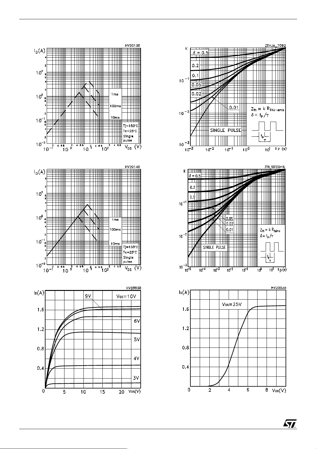
Figure 3: Safe Operating Area For TO-92
Figure 4: Safe Operating Area For SOT23-3L
Figure 6: Thermal Impedance For TO-92
Figure 7: Thermal Impedance For SOT23-3L
Figure 5: Output Characteristics
4/11
Figure 8: Transfer Characteristics

2N7000 - 2N7002
Figure 9: Transconductance
Figure 10: Gate Charge vs Gate-source Voltage
Figure 12: Static Drain-source On Resistance
Figure 13: Capacitance Variations
Figure 11: Normalized Gate Threshold Voltage vs Temperature
Figure 14: Normalized On Resist ance vs Temperature
5/11

2N7000 - 2N7002
Figure 15: Source-Dr ain Forward Charact eristics
Figure 16: Normalized BVDSS vs Temperature
6/11

2N7000 - 2N7002
Figure 17: Unclamped Inductive Load Test Circuit
Figure 18: Switching Times Test Circuit For Resistive Load
Figure 20: Unclamped Inductive Wafeform
Figure 21: Gate Charge Test Circuit
Figure 19: Test Circuit For Inductive Load Switching and Diode Recovery Times
7/11

2N7000 - 2N7002
TO-92 MECHANICAL DATA
DIM.
A 4.32 4.95 0.170 0.194
b 0.36 0.51 0.014 0.020
D 4.45 4.95 0.175 0.194
E 3.30 3.94 0.130 0.155
e 2.41 2.67 0.094 0.105
e1 1.14 1.40 0.044 0.055
L 12.70 15.49 0.50 0.610
R 2.16 2.41 0.085 0.094
S1 0.92 1.52 0.036 0.060
W 0.41 0.56 0.016 0.022
V5° 5°
MIN. TYP MAX. MIN. TYP. MAX.
mm. inch
8/11

SOT23-3L MECHANICAL DATA
2N7000 - 2N7002
DIM.
mm. mils
MIN. TYP MAX. MIN. TYP. MAX.
A 0.890 1.120 35.05 44.12
A1 0.010 0.100 0.39 3.94
A2 0.880 0.950 1.020 34.65 37.41 40.17
b 0.300 0.500 11.81 19.69
C 0.080 0.200 3.15 7.88
D 2.800 2.900 3.040 110.26 114.17 119.72
E 2.100 2.64 82.70 103.96
E1 1.200 1.300 1.400 47.26 51.19 55.13
e 0.950 37.41
e1 1.900 74.82
L 0.400 0.600 15.75 23.63
L1 0.540 21.27
k8°8°
D
e
GAUGE
PLANE
0.25
L
L1
E
SEATING
PLANE
C
E1
b
e1
A2
A
c
C
0.10
7110469/A
A1
9/11

2N7000 - 2N7002
Table 8: Revision History
Date Revision Description of Changes
06-Apr-2005 2 New stylesheet
20-Apr-2005 3 New Pin Configuration for TO-92
10/11

2N7000 - 2N7002
Information furnished is believed to be accurate and reliable. However, STMicroelectronics assumes no responsibility for the consequences
of use of such information nor for any infringement of patents or other rights of third parties which may result from its use. No license is granted
by implication or otherwise under any patent or patent rights of STMicroelectronics. Specifications mentioned in this publication are subject
to change without notice. This publication supersedes and replaces all information previously supplied. STMicroelectronics products are not
authorized for use as critical components in life support devices or systems without express written approval of STMicroelectronics.
The ST logo is a registered trademark of STMicroelectronics
All other names are the property of their respective owners
© 2005 STMicroelectronics - All Rights Reserved
STMicroelectronics group of companies
Australia - Belgium - Brazil - Canada - China - Czech Republic - Finland - France - Germany - Hong Kong - India - Israel - Italy - Japan -
Malaysia - Malta - Morocco - Singapore - Spain - Sweden - Switzerland - United Kingdom - United States of America
11/11
 Loading...