ST Microelectronics 2425C2DB Users Manual

SPBT2425C2DB.xxx
June 2007
FEATURES
- Bluetooth V2.0 board
- Serial interface on DB9 connector
- USB connection
- PCB antenna on board
- Single 5 V supply voltage
- CE compliant
- FCC compliant
FCC ID: S9N2425C2DB
User Manual
DESCRIPTION
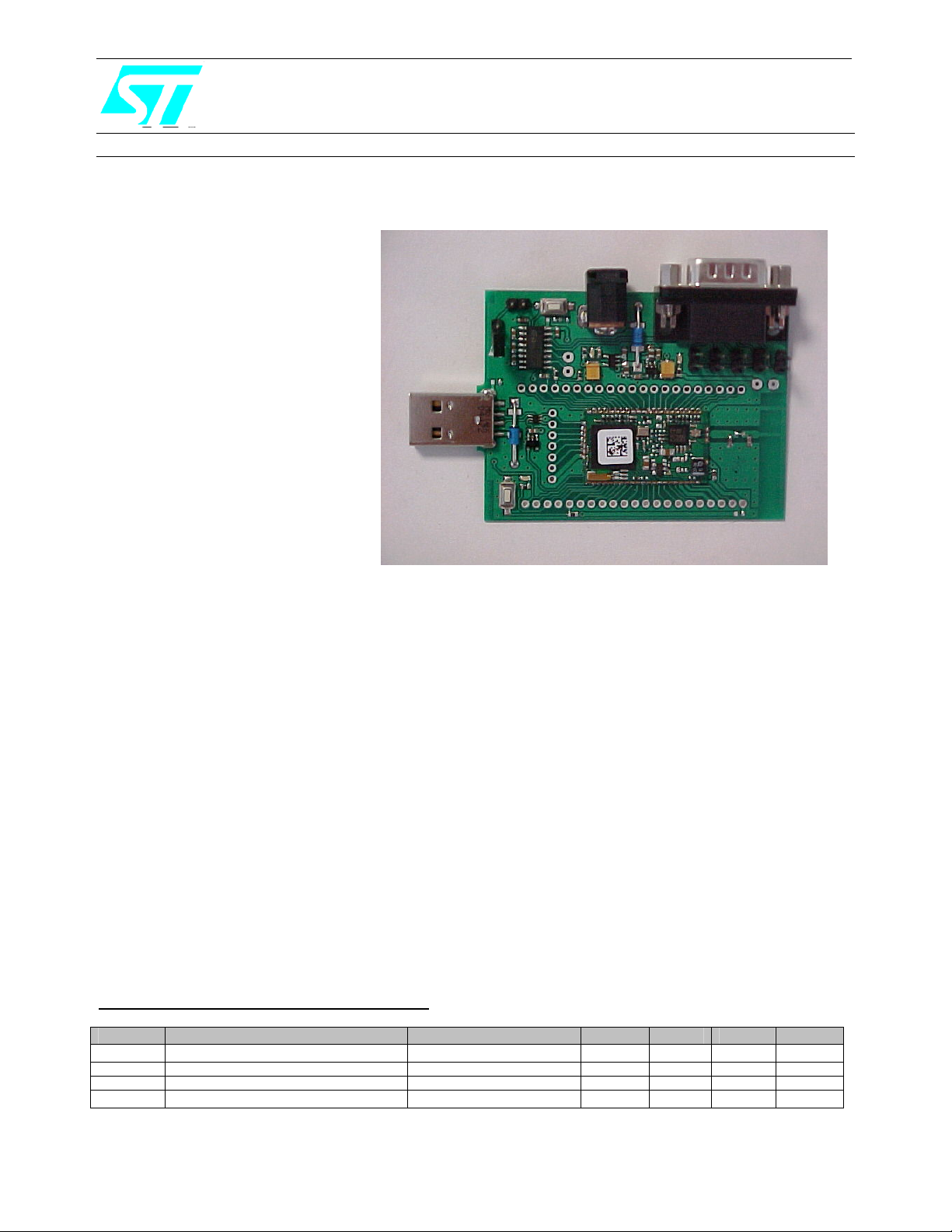
SPBT2425C2DB.xxx is a Bluetooth Class2 Demoboard for SPBT2425C2 Bluetooth module including the RF antenna.
Suffix xxx identifies the Firmware release : H for HCI commands and AT1 for AT commands.
SPBT2425C2DB.H is a board with a downloaded FW which enables the user to interface the Bluetooth module with HCI
commands.
SPBT2425C2DB.AT1 is a board with a downloaded FW which enables the user to create a Bluetooth link with simple AT
commands.
AT commands are sent by means the serial line which is accessible by the DB9 connector.
SPBT2425C2DB.xxx board can be supplied by an external 5V DC source or via the USB port.
1 - RECOMMENDED OPERATING CONDITIONS
Symbol Parameter Conditions Min Typ Max Unit
VDD Board Supply voltage -20°C < T < 70°C 4 5 6 V
Tstg Operating ambient temperature -20 +70 °C

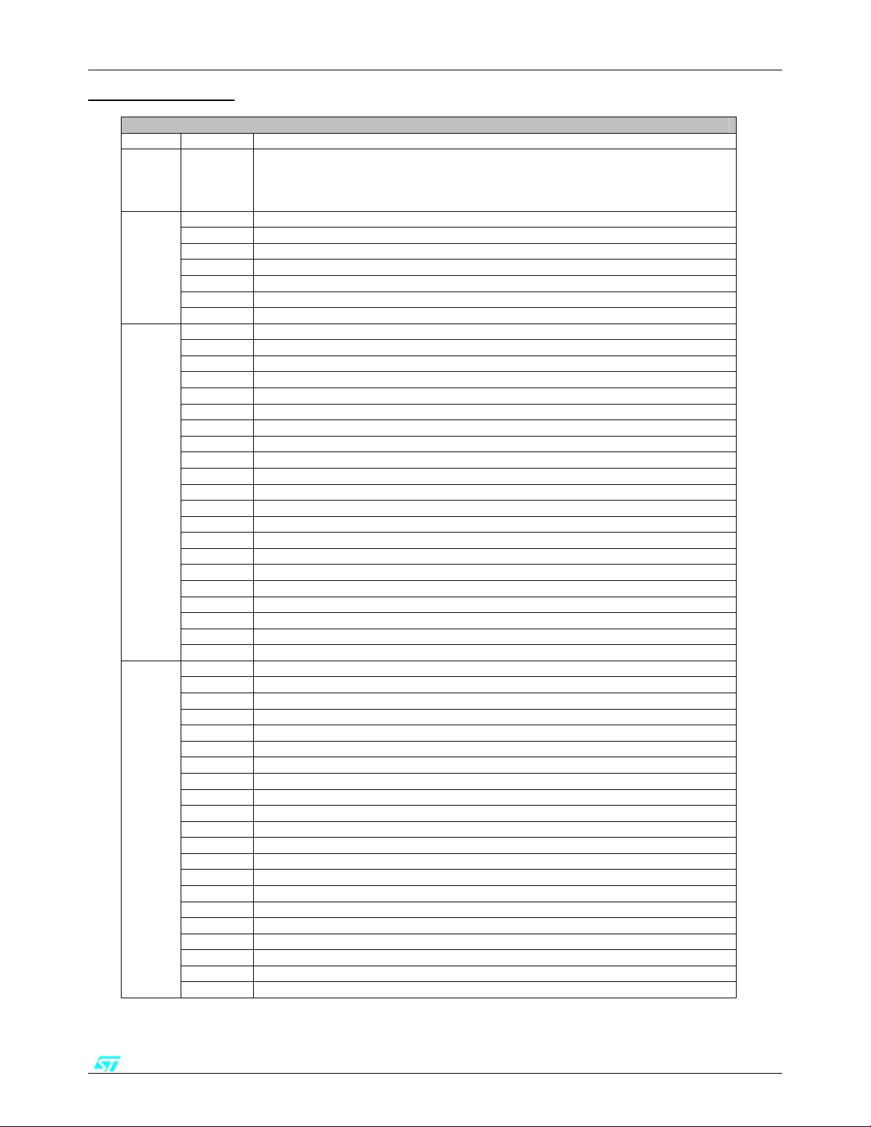
2 - I/O CONNECTIONS
J1 Vcc Power supply plug ( 5V )
USB Port
J2
1 USB_DN
2 USB_DP
3 SPI_FRM
J3
4 SPI_CLK
5 SPI_TXD
6 SPI_RXD
7 GND
1 Boot
2 GPIO 0
3 GPIO 1
4 GPIO 2
5 GPIO 3
6 GPIO 4
7 GPIO 5
8 GPIO 6
9 GPIO 7
10 GPIO 8
J4
11 GPIO 9
12 LP_CK
13 GPIO 11
14 GPIO 12
15 GPIO 13
16 GPIO 14
17 GPIO 15
18 1.8V
19 2.8V
20 INHIBIT
21 VDD
1 RX_EN
2 PA_EN
3 PA_V1
4 PA_V0
5 ANT_SW
6 PCM_A
7 PCM_B
8 PCM_SYNC
9 PCM_CLK
10 NTRST
J5
11 TDI
12 TMS
13 TCK
14 TDO
15 13 MHz out
16 RESET
17 INT2
18 RXD
19 TXD
20 I2C0
21 I2C1
SPBT2425C2DB.xxx
DESCRIPTION
When the USB port is connected , the 5V USB is used to supply the BT m odule ( by
means a voltage regulator) and the board i tself
When USB port is used 5V on J1 power plug can be avoided
rev. 1.0 18-Jun-07 2/9

SPBT2425C2DB.xxx
DESCRIPTION
Serial line port ( DB9 male connector)
J6
On board is present a level translator to ada pt the BT module digital levels to the
RS232 standard levels.
1 Boot signal - If connected to GND the module can perform the dowloading – see also
J7
JP6
2 Reset signal - A low level on this pin force the module in reset state - see also S 2
JP1 DB9 connector connectio n – see electrical drawing
JP2 DB9 connector connectio n – see electrical drawing
JP3 DB9 connector connectio n – see electrical drawing
JP4 DB9 connector connectio n – see electrical drawing
JP5 DB9 connector connectio n – see electrical drawing
JP6
S1
Boot
If connected to GND the module can perform the dowloading
N.O. push button connected to BT module GPIO3; when activated a Low level is
applied to GPIO6 otherwise GPIO6 is at High level.
S2 Reset – Push button acting on the module reset pin
L1 LED connec ted to BT module GPIO1 .
L2 LED showing the presence of the 2.8 V internal voltage (2.8 V modu le version )
L3 LED showing the presence of the 3.3 V internal voltage (3.3 V modu le version )
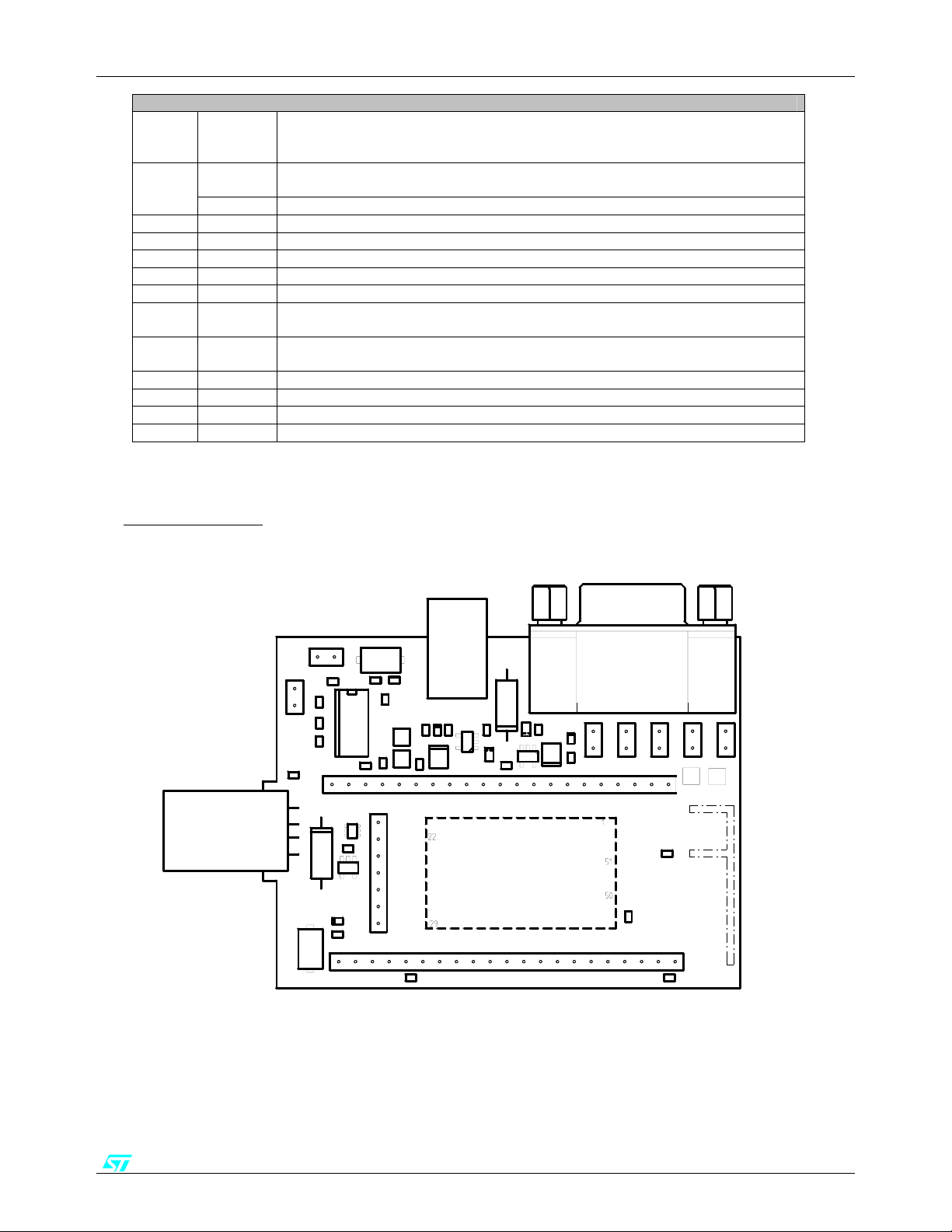
3 - BOARD LAYOUT
J7
1
C7
JP6
C9
1
C10
C11
C6
21
J2
1
D2
S1
L1
S2
R8
C12
C8
TP1
TP2
1
J3
7
R1
R3
U4
R6
U3
C5
U2
R2
1
R7
J1
R10L3C4
C1
C3
U1
CLASS 1.5 MODULE
C2
C17
D1
C16
L2
C15
U5
C18
R9
J5
BT1
J4
JP5
J6
JP2
R5
6
1
1
JP3
1
C19
1
1
JP4
TP4
TP3
ANT1
21
R4
9
5
1
rev. 1.0 18-Jun-07 3/9
JP1
1
 Loading...