

Page 1
GSBT2416C2DB.xxx
User manual
June 2007
FEATURES
- Bluetooth V1.2 board
- Serial interface on DB9 connector
- USB connection
- PCB antenna on board
- Single 5 V supply voltage
- CE compliant
- FCC compliant
FCC ID: S9N16C2
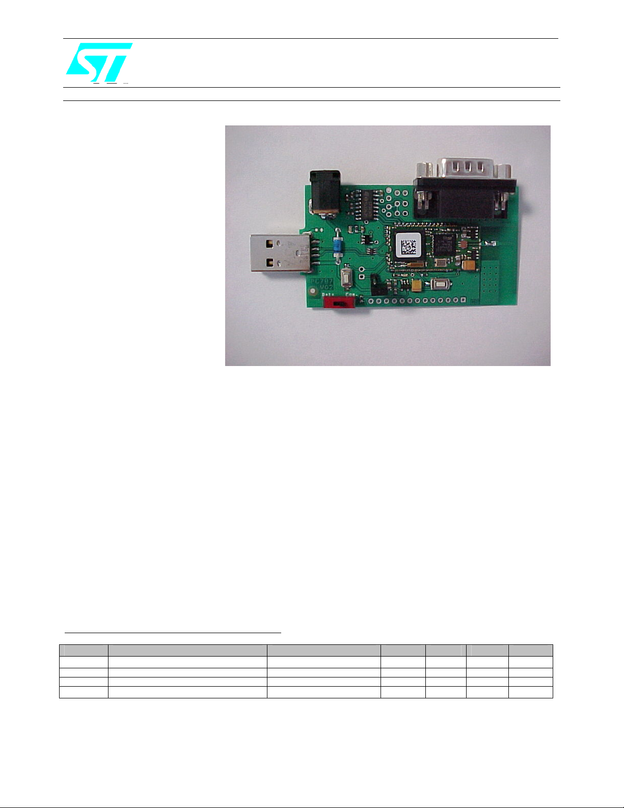
DESCRIPTION
GSBT2416C2DB.xxx is a Bluetooth Class2 Demoboard for GSBT2416C2 Bluetooth module including the RF antenna.
Suffix xxx identify the Firmware release : no suffix for HCI commands and AT1 for AT commands.
GSBT2416C2DB. is a board with a downloaded FW which enables the user to to interface the Bluetooth module with HCI
commands.
GSBT2416C2DB.AT1 is a board with a downloaded FW which enables the user to create a Bluetooth link with simple AT
commands.
AT commands are sent by means the serial line which is accessible by the DB9 connector.
SPBT2425C2DB.xxx board can be supplied by an external 5V DC source or via the USB port
1 - RECOMMENDED OPERATING CONDITIONS
Symbol Parameter Conditions Min Typ Max Unit
VDD Board Supply voltage -20°C < T < 70°C 4 5 6 V
Tstg Operating ambient temperature -20 +70 °C
Page 2

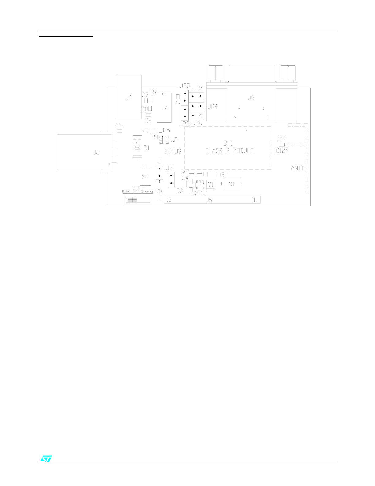
2 - I/O CONNECTIONS
1 Boot signal - If connected to GND the module can perform the dowloading – see also
J1
2 Reset signal - A low level on this pin force the module in reset state - see also S3
USB Port
J2
Serial line port ( DB9 male connector)
J3
J4
Vcc Power supply plug ( 5V )
1 GPIO 15
2 GPIO 14
3 GPIO 13
4 GPIO 12
5 GPIO 11
6 GPIO 10
J5
7 GPIO 9
8 GPIO 8
9 GPIO 7
10 GPIO 4
11 GPIO 3
12 GPIO 2
13 GPIO 0
JP1
Boot
JP2 DB9 connector connection – see electrical drawing
JP3 DB9 connector connection – see electrical drawing
JP4 DB9 connector connection – see electrical drawing
JP5 DB9 connector connection – see electrical drawing
JP6 DB9 connector connection – see electrical drawing
N.O. push button connected to BT module GPIO6; when activated a Low level is
S1
S2
Switch connected to GPIO3 ( 10 KΩ pullup to 3.3V)
S3 Reset – Push button acting on the module reset pin
L1
L2
LED connected to BT module GPIO1 .
LED showing the presence of the 3.3V internal voltage – Bluetooth module supply
GSBT2416C2DB.xxx
DESCRIPTION
JP1
When the USB port is connected , the 5V USB is used ( by the 3.3V regulator) to
supply the BT module and the board itself
When USB port is used do not supply an ext. 5V to J4 power plug
USB port is not used for AT version
On board is present a level translator to adapt the BT module digital levels to the
RS232 standard levels.
When 5v input is used on J4 plug do not connect USB port
If connected to GND the module can perform the dowloading
applied to GPIO6 otherwise GPIO6 is at High level.
Not used for AT commands version
In AT version this switch is used to select Command / Data mode
On AT version this led shows when a Bluetooth conn ection is ON (led ON )
voltage
rev. 1.0 18-Jun-07 2/13
Page 3
GSBT2416C2DB.xxx
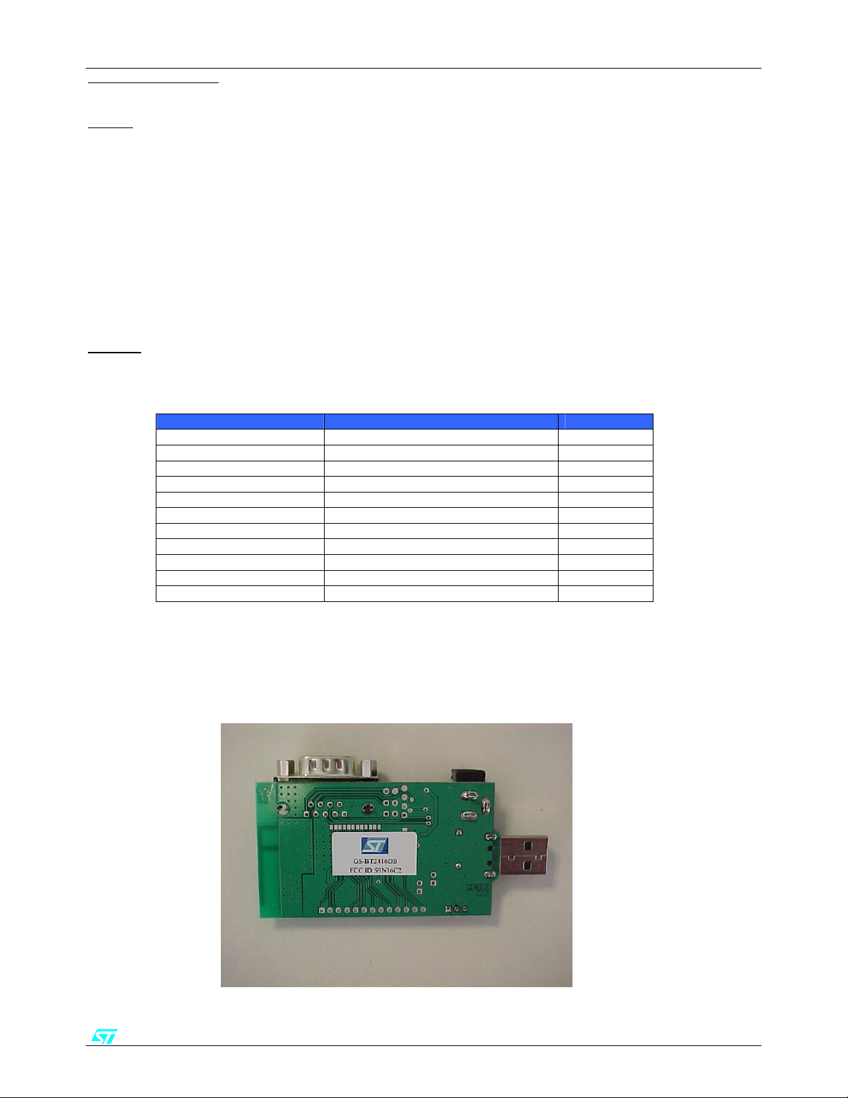
3 - BOARD LAYOUT
rev. 1.0 18-Jun-07 3/13
Page 4
GSBT2416C2DB.xxx
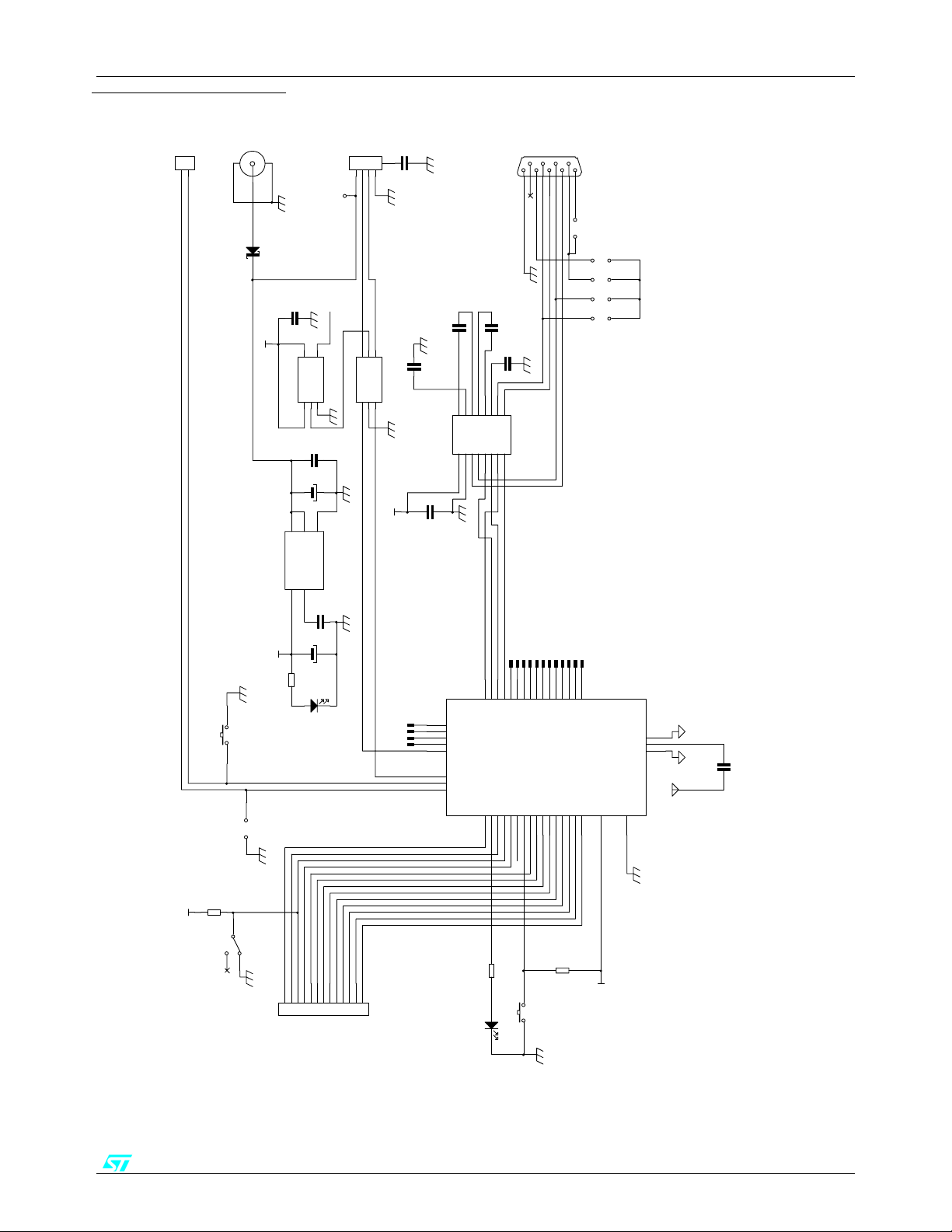
4 - ELECTRICAL DRAWING
J1
1
2
RESET
BOOT
J4
PLUG
3
2
1
GND
Vext+5V
D1 BYV10-60
C5
100n
+3.3V
5
Vcc
I/O1O/I2GND
U2 74V1G66CTR
USB (Vcc)
123
J2
USB CON.
USB +5V
GPIO5
4
C
3
C4
100n
C3
10u
6.3V
C11
USB (D-)
4
D3
3
NM
USB (GND)
USB (D+)
4
C8 100n
6
5
D4
3.3V
D11GND2D2
C7
100n
U3 USBUF01W6
U4 ST3232
C10 100n
2
8
7
4
1
3
5
6
V-
V+
C1-
C2-
C2+
C1+
R2in
T2out
R2out9T2in
GND15T1out
T1in
R1in13R1out12Vcc
10
14
11
16
594837261
PC DTR
GND
C9
100n
J3
PC_RTS
PC_RX
PC_CTS
PC DSR
PC_TX
JP2
JP6
JP5
JP4
JP3
NM = NOT MOUNTED
1
2
3
Vin
GND
INHIBIT
ByPass4Vout
U1 LD2985BM33R
5
C2
10n
+3.3V
C6
100n
C1
22u
+3.3V
R4
S3
JP1
FOR INTERNAL FLASH
PROGRAMMING
6.3V
BT1
470 Ohm
L2
GREEN
SPI_FRM
17
SPI_CLK
18
SPI_TXD
19
SPI_RXD
20
USB_DN
21
USB_DP
22
RESET
23
BOOT
24
16
GPIO025GPIO126GPIO227GPIO328GPIO429GPIO530GPIO631GPIO732GPIO833GPIO934GPIO1135GPIO1036GPIO1237GPIO1338GPIO1439GPIO15
8
13
6
14
11
PCM_A12PCM_B
(UART_TX) TXD
(UART_RX) RXD
(UART_CTS) CTS15(UART_RTS) RTS
GPIO5
3
10
4
2
5
9
INT1
PCM_CLK
PCM_SYN C
GPIO6
(JTAG2) TMS
(JTAG3) TCK
(JTAG4) TDO
(JTAG0) NTRST
(I2C_DAT) I2C07(I2C_CLK) I2C 1
BLUETOOTH MODULE GS-BT2416C2
1
VIN (VDDIO)41GND
RF-GND
45
ANT
44
RF-GND
43
42
ANT1
ANTENNA BLU ETOOTH
(JTA G 1 ) TD I
40
R3
10K
+3.3V
2
S2
1
3
Data
Command
12345678910111213
J5
GPIO1
R2
470 Ohm
L1
GREEN
R1
10K
S1
+3.3V
rev. 1.0 18-Jun-07 4/13
C12 39pF
Page 5
GSBT2416C2DB.xxx
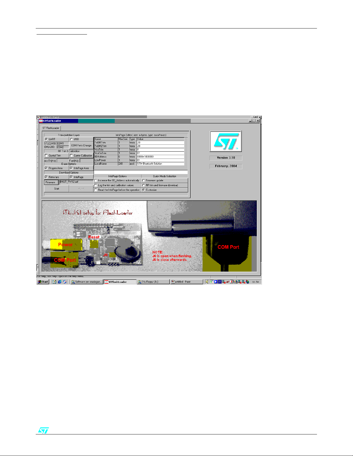
5 - DOWNLOADING
GSBT2416C2DB.xxx has also the possibility to be downloaded with a file developed by the user
To download a file into GSBT2416C2DB the below items must be followed:
- connect the board to a PC by means a RS232 cable connected on COM1 / COM2
- put a jumper on JP1 ( Boot pin to low level)
- connect the power supply cable to the board at +5V ext Vin
- open the “Flash loader “ program
- choose UART on Transportation layer section
- choose the appropriate COM1 / COM2 port
- choose the firmware to be downloaded on “Firmware “ section
- press start : on the dialog bar will appear “ reset the board”
- power the board ( a reset is generated) : on the dialog bar will appear the % of the downloading.
rev. 1.0 18-Jun-07 5/13
Page 6
GSBT2416C2DB.xxx
6 - CERTIFICATIONS
6.1 - CE
Measurements have been performed in accordance with ( report available on request):
EN 300 328 V 1.6.1 (2004-11) : “ Electromagnetic compatibility and radio spectrum Matters (ERM); Wideband Transmission
Systems; Data transmission equipment operating in the 2.4GHZ ISM band and using wide band modulation techniques;
Harmonized EN covering essential requirements under article 3.2 of the R&TTE directive”
EN 301 489-17 V 1.2.1 :2002: “ Electromagnetic compatibility and radio spectrum Matters (ERM); ElectroMagnetic
Compatibility (EMC) standard for radio equipment and services ; Part 17: Specific condition for 2.4GHz wideband transmission
systems and 5 GHz High performance RLAN equipment.”
EN 60950-1 : “Information technology equipment -Safety –Part 1 : General requirements “
6.2 - FCC
To get compliance with FCC CFR47 part15 the following tests have been performed:
CFR47 part 15 section Title Result
15.203 15.247 (b) (4) (i) Antenna requirements
15.247 (a) Conducted emission
15.209 (a) (f) Radiated emission
15.247 (a) Frequency hopping –Spread Spectrum Spec
15.247 (b) Maximum Peak Output power
15.247 (d) 100 kHz Bandwidth of Frequency Band Edges
15.247 (d) Conducted emission
15.247 (e) Power Spectral density
15.247 (g) FHSS transmission characteristics
15.247 (i) (§47CFR1.1307 (b)(1)) RF Humane exposure
pass
pass
pass
pass
pass
pass
pass
pass
pass
pass
This board has the following FCC ID:
FCC ID:S9N16C2
rev. 1.0 18-Jun-07 6/13
Page 7

GSBT2416C2DB.xxx
FCC Statement
This device complies with Part 15 of the FCC Rules. Operation is subject to the following two conditions:
(1) this device may not cause harmful interference, and (2) this device must accept any interference received, including
interference that may cause undesired operation.
NOTE: This equipment has been tested and found to comply with the limits for a Class B digital device, pursuant to Part 15 of
the FCC Rules. These limits are designed to provide reasonable protection against harmful interference in a residential
installation. This equipment generates, uses and can radiate radio frequency energy and, if not installed and used in accordance
with the instructions, may cause harmful interference to radio communications.
However, there is no guarantee that interference will not occur in a particular installation.
If this equipment does cause harmful interference to radio or television reception, which can be determined by turning the
equipment off and on, the user is encouraged to try to correct the interference by one or more of the following measures:
- Reorient or relocate the receiving antenna
- Increase the separation between the equipment and receiver
- Connect the equipment into an outlet on a circuit different from that to which the receiver is connected
Consult the dealer or an experienced radio/TV technician for help.
Antenna
Our board type GS-BT2416C2DB.xxx is for OEM integrations only. The end-user product will be
professionally installed in such a manner that only the authorized antennas are used.
Caution
Any changes or modifications not expressed approved by the party responsible for compliance could cause the module to cease
to comply with FCC rules part 15, and thus void the user’s authority to operate the equipment.
Label instruction
Module type : Bluetooth class 2 board GSBT2416C2DB.xxx (GSBT2416C2 module + PC 787 carrier
board)
FCC-ID : S9N16C2
This intends to inform you how to specify the FCC ID of our Bluetooth board GSBT2416C2DB.xxx on your final
product.
Based on the Public Notice from FCC, the product into which the our transmitter module is installed must display a
label referring to the enclosed module.
The label should use wording such as “Contains Transmitter module FCC ID: S9N16C2 or “Contains FCC ID:
S9N16C2, any similar wording that expressed the same meaning may be use.
It shows an example below
Contains FCC ID: S9N16C2
rev. 1.0 18-Jun-07 7/13
Page 8

GSBT2416C2DB.xxx
Special requirement for Modular application
The following requirements are fulfilled:
1)
The modular transmitter must have its own RF shielding:
The RF module fulfils the emission requirements of the FCC rules without additional shielding.
The modular transmitter must have buffered modulation/data inputs:
2)
The module has a memory management unit inside of the IC. The processor interfacing with the external application by means
general purpose I/O ( GPIO) , Uart, USB, PCM, I2C, SPI. The processor interfaces also the RF part of the module exchanging
data and commend with it. Inside the processor a flash memory is available to download the customer application and the
Bluetooth profiles.
3)
The modular transmitter must have its own power supply regulation:
The module contains an own voltage regulation. In case of changes in the supply voltage VCC (for example caused by
temperature changes or other effects), the internal voltage will be stabilized.
The modular transmitter must comply with the antenna requirements of Section 15.203 and 15.204:
4)
The RF module is for OEM (Original Equipment Manufacturer) integration only. The end-user product will be professionally
installed in such a manner that only the authorized antenna is used.
The modular transmitter must be tested in a stand-alone configuration:
5)
The RF module was tested in a stand-alone configuration.
6)
The modular transmitter must be labelled with its own FCC ID number:
The RF module will be labelled with its own FCC ID number. When the module is installed inside the end-product, the label is
not visible. The OEM manufacturer is instructed how to apply the exterior label.
The modular transmitter must comply with any specific rule or operating requirements applicable to the transmitter and the
7)
manufacturer must provide adequate instructions along with the module to explain any such requirements:
The EUT is compliant with all applicable FCC rules. Detail instructions are given in the product Users Guide.
8)
The modular transmitter must comply with any applicable RF exposure requirements.
Maximum measured power output: 1,08 mW (0,33 dBm)
-
-
Maximum antenna gain: 1 dBi = numeric gain 1,259 (see also FCC test report)
Maximum permissible exposure defined in 47 CFR 1.1310: 1 mW/cm².
The RF module operates at low power level so it does not exceed the Commission’s RF exposure guidelines limits; furthermore,
Spread spectrum transmitters operate according to the Section 15.247 are categorically excluded from routine environmental
evaluation.
rev. 1.0 18-Jun-07 8/13
Page 9

GSBT2416C2DB.xxx
7 - AT COMMANDS APPENDIX
This section is applicable to demoboard with AT command FW downloaded ( GSBT2416C2DB.AT1 )
Purpose of this section is to describe all the necessary steps to establish a connection between two Bluetooth
GS-BT2416C2DB.AT1 demo boards in a Serial line /Cable replacement application.
( This connection example is also reported on OBSTFW-101 datasheet, Application Not es (vers 1.6))
SETUP & CONNECT
To perform the connection you need two PC and two GS-BT2416C2DB.AT1 boards.
Steps to connect.
( please refer to OBSTFW-101v 1.2.1.8 datasheet for the meaning of AT commands)
- Fix a GS-BT2416C2DB.AT1 board to be used as “Client” and suppose it has the address 0080E1000001.
Hereafter this board will be called “Client”
- Fix a GS-BT2416C2DB.AT1 board to be used as “Server” and suppose it has the address 0080E1000002.
Hereafter this board will be called “Server”
- Connect the Server board to a PC by means a RS232 cable
- Connect the Client board to a PC by means a RS232 cable
- Open on both the PCs HyperTerminal program and set the communication line with the following parameters:
o Select the proper COM line ( COM1, COM2……)
o baud rate : 9600 ( default baud rate of GSBT2416C1/AT module)
o data bits: 8
o parity : none
o stop bits : 1
o flow control : none
o In ASCII setup ,set flag line ends with line feed
o In ASCII setup , set flag echo characters typed locally
- Power with the external 5V the Client board : on the PC screen connected to the Client should appear +READY
- Power with the external 5V the Server board : on the PC screen connected to the Server should appear +READY
- Configure the Client board by means the following commands:
( GPIO3 Client must be Low to select Command Mode – S2 switch in Command mode)
Command Answer
AT OK Check module ready
AT+BTCMODE=0 OK
AT+BTPMODE=1 OK
AT+BTDMODE=0 OK Not Discoverable
AT+BTSECMODE=1 OK
AT+BTENCMODE=0 OK
AT+BTNAME=”SPP Client” OK Set client name
AT+BTCLASS=52020C OK
rev. 1.0 18-Jun-07 9/13
Page 10

GSBT2416C2DB.xxx
- Configure the Server board by means the following commands:
( GPIO3 Server must be Low to select Command Mode– S2 switch in Command mode )
Command Answer
AT OK Check module ready
AT+BTCMODE=1 OK
AT+BTPMODE=1 OK
AT+BTDMODE=1 OK Discoverable
AT+BTSECMODE=1 OK
AT+BTENCMODE=0 OK
AT+BTPINCODE=”1234” OK Pin code
AT+BTNAME=”SPP Server” OK Set server name
AT+BTCLASS=52020C OK
AT+BTREGPORT=”SPP port” OK Name of service offered
After the Server board configuration , Server board GPIO3 must be put HIGH to select DATA MODE enabling the
Server board to receive and transmit DATA.
- Inquiry & available Services
Before to establish a connection, the Client has to know which Bluetooth devices are present and which services are
offered, and therefore the Client:
- will perform first the inquiry by the command:
AT+BTINQ=xx where xx is the inquiry time (i.e. 10 sec -> AT+BTINQ=10 )
The answer will be a list of present Bluetooth connectable devices, one of the device should be our SPP Server:
+BTINQRES:0080E1000002,”SPP Server”
OK
- and after will ask for which kind of service is available with the command:
AT+BTRPORTS=0080E1000002
The answer will be :
+BTRPORT:”SPP Port”,1 serial port profile , port 1 (can be 1,2…)
OK
- Once known the device present, the service offered, the Client finalize the connection with the command :
AT+BTCONNECT=0080E1000002,1,”1234”,1,0
OK
At this point the connection is established and GPIO1 (indicating the connection status) on both Client and Server
boards becomes high.
On the GS-BT2416C1AT1 board a led is connected to GPIO1 and therefore the connection is shown also by a led on.
GPIO3 on Client board must be now put at HIGH level allowing the Client to send and receive DATA from Server.
- Disconnection
To disconnect, the Client has to put its GPIO3 LOW ( Command mode) ( the changing from high to low on GPIO3 is
signaled on the Client PC screen with +READY) and send the command :
AT+BTDISCONNECT
OK
The result will be the disconnection of the link Client / Server and GPIO1 on both Client and Server boards will return
to low ( the leds will go off ).
rev. 1.0 18-Jun-07 10/13
Page 11

GSBT2416C2DB.xxx
MACRO INSTRUCTIONS
With the version 1.2.1.8 of OBSTFW -101 has been introduced the MACRO concept with the commands
AT+BTMACROSTART , AT+BTMACROSTOP and AT+MACROCLEAR.
These commands work in such a way that all the commands written between AT+BTMACROSTART and
AT+BTMACROSTOP commands will be stored inside the internal flash memory and executed at each power up of the
module.
Take note that when you insert a command between MACROSTART and MACROSTOP you have not the immediate
execution of the command but only the storing in the flash memory, the module will answer with OK or ERROR from a
syntax point of view.; execution will be active at the next power on.
That means, after the writing of the commands between the two macro commands, the module could work in a stand
alone way without the need to program it at each power on.
MACROCLEAR command will erase all the commands stored.
As an example: suppose to have always the previous modules with final address 01 (client) and 02 ( server) and to
know already which connection to get .
Write the following sequence of commands in client and server module , after the MACROSTOP command it will be
stored into the internal memory of the correspondent module .
Client Server
AT+BTMACROSTART AT+BTMACROSTART
AT+BTCMODE=0 AT+BTCMODE=1
AT+BTPMODE=1 AT+BTPMODE=1
AT+BTDMODE=0 AT+BTDMODE=1
AT+BTSECMODE=1 AT+BTSECMODE=1
AT+BTENCMODE=0 AT+BTENCMODE=0
AT+BTNAME=”SPP Client” AT+BTPINCODE=”1234”
AT+BTCLASS=52020C AT+BTNAME=”SPP Server”
AT+BTCONNECT=0080E1000002,1,”1234”,10,5 AT+BTCLASS=52020C
AT+BTMACROSTOP AT+BTREGPORT=”SPP port”
AT+BTMACROSTOP
Note that :
- As the address module to connect is know , the inquiry command can be omitted
- In BTCONNECT command has been set 10 retry at 5 sec interval.
After the modules have been programmed, you can power off and power on again the modules themselves; you will
see that at a certain point the modules will be connected each other ( led on) without any intervention .
Is not important to power on before the server or the client ; the only rule to follow is ,once the client has been powered
on, getting the server powered in the time fixed by the 10 retry at 5 sec interval.
During the macro execution the module will answer with “OK or “ERROR” for each command executed; if this
feedback is not wished ,it can be avoided with the AT+ECHO=OFF command.
MODULE BT ADDRESS
Each module has its own address which identify the module itself in the network; for the above examples have been
always taken in consideration addresses 0080E1000001 and 0080E1000002.
Modules on GS-BT2416C1AT1 board could have different addresses ; before to start sending commands, the module
address can be found with the command AT+BTSETTINGS=? which will show the relevant information of the
module including the BT address.
rev. 1.0 18-Jun-07 11/13
Page 12

GSBT2416C2DB.xxx
POINT to POINT CONNECTION
Modules with AT commands firmware can only perform point to point connection which means only a connection per
time can be activated.
A module can be connected with several other modules but it has to disconnect the previous connection before to
activate a new one.
Suppose to have a Client C1 which need to connect with Server S1,S2,..Sn :
S1
C1
S2
Sn
In this case the procedure to follow is the following :
- C1 will establish the connection with S1 exchanging the data
- C1 will disconnect S1 with the command AT+BTDISCONNECT
- C1 will establish the connection with S2 exchanging the data
- C1 will disconnect S2 with the command AT+BTDISCONNECT
- C1 will establish the connection with Sn exchanging the data… an so on
rev. 1.0 18-Jun-07 12/13
Page 13

GSBT2416C2DB.xxx
Information furnished is believed to be accurate and reliable. However, STMicroelectronics assumes no responsibility for the consequences of use of
such information nor for any infringement of patents or other rights of thir d parties which may result from its use. No license is granted by implication
or otherwise under any patent or patent rights of STMicroelectronics. Specifications mentioned in this publication are subject to change without
notice. This publication supersedes and replaces all information previously supplied. STMicroelectronics products are not authorized for use as critical
http://www.st.com
components in life support devices or systems without express written approval of STMicroelectronics.
The ST logo is a registered trademark of STMicroelectronics
© 2007 STMicroelectronics - All Rights Reserved
STMicroelectronics GROUP OF COMPANIES
Australia - Brazil - China - Finland - France - Germany - Hong Kong - India - Italy - Japan - Malaysia - Malta - Morocco
Singapore - Spain - Sweden - Switzerland - United Kingdom - U.S.A.
rev. 1.0 18-Jun-07 13/13
 Loading...