

Page 1

AN5398
Application note
ISM330DHCX: always-on 3D accelerometer and 3D gyroscope with digital output
for industrial applications
Introduction
This document is intended to provide usage information and application hints related to ST’s ISM330DHCX iNEMO inertial
module.
The ISM330DHCX is a system-in-package featuring a high-accuracy and high-performance 3D digital accelerometer and 3D
digital gyroscope tailored for Industry 4.0 applications.
All the design aspects and the testing and calibration of the ISM330DHCX have been optimized to reach superior accuracy,
stability, and extremely low noise.
The ISM330DHCX has a 3D accelerometer capable of wide bandwidth, ultra-low noise and a selectable full-scale range of
±2/±4/±8/±16 g. The 3D gyroscope has an angular rate range of ±125/±250/±500/±1000/±2000/±4000 dps and offers superior
stability over temperature and time along with ultra-low noise.
The unique set of embedded features facilitates the implementation of smart and complex sensor nodes which deliver high
performance at very low power:
• its capability to support up to 16 embedded finite state machines that can be programmed and run independently to detect
and classify complex motion sequences.
• the embedded Machine Learning Core logic allows identifying if a data pattern matches a user-defined set of classes. A
typical example of an application is the identification and detection of multiple complex motion patterns.
• the integrated smart first-in first-out (FIFO) buffer of up to 9 kbyte size allows dynamic batching of significant data (i.e.
internal and external sensors, timestamp and temperature).
The ISM330DHCX is available in a small plastic land grid array (LGA) package of 2.5 x 3.0 x 0.83 mm.
AN5398 - Rev 3 - January 2021
For further information contact your local STMicroelectronics sales office.
www.st.com
Page 2

1 Pin description
AN5398
Pin description
Figure 1. Pin connections
AN5398 - Rev 3
page 2/132
Page 3

AN5398
- Rev 3
page 3/132
Table 1. Pin status
Pin # Name
SDO
1
SA0
2 SDx Connect to VDDIO or GND
3 SCx Connect to VDDIO or GND
INT1
INT2
(2)
(3)
4
5 Vdd_IO Power supply for I/O pins Power supply for I/O pins Power supply for I/O pins
6 GND 0 V supply 0 V supply 0 V supply
7 GND 0 V supply 0 V supply 0 V supply
8 Vdd Power supply Power supply Power supply
9
10 OCS_Aux
11 SDO_Aux
12 CS
13 SCL
14 SDA
Mode 1 function
SPI 4-wire interface serial data
output (SDO)
I²C least significant bit of the device
address (SA0)
Programmable interrupt 1 Programmable interrupt 1 Programmable interrupt 1 Default: input with pull-down. Default: input with pull-down. Default: input with pull-down.
Programmable interrupt 2 (INT2) /
Data enabled (DEN)
Connect to VDDIO or leave
unconnected
Connect to VDDIO or leave
unconnected
I²C/SPI mode selection (1:SPI idle
mode / I²C communication enabled;
0: SPI communication mode / I²C
disabled)
I²C serial clock (SCL) / SPI serial port
I²C serial data (SDA) / SPI serial data
clock (SPC)
input (SDI) / 3-wire interface serial
data output (SDO)
(1)
Mode 2 function
SPI 4-wire interface serial data
output (SDO)
I²C least significant bit of the device
address (SA0)
I²C serial data master
I²C serial clock master
Programmable interrupt 2 (INT2) /
Data enabled (DEN) / I²C master
external synchronization signal
(MDRDY)
Connect to VDDIO or leave
unconnected
Connect to VDDIO or leave
unconnected
I²C/SPI mode selection (1:SPI idle
mode / I²C communication enabled;
0: SPI communication mode / I²C
disabled)
I²C serial clock (SCL) / SPI serial port
I²C serial data (SDA) / SPI serial data
clock (SPC)
input (SDI) / 3-wire interface serial
data output (SDO)
1. Refer to description in Section 3.6 Connection modes.
2. INT1 must be set to '0' or left unconnected during power-on. If no interrupt signal is needed on INT1, this pin can be left unconnected.
3. If no interrupt signal is needed on INT2, this pin can be left unconnected.
(MSDA)
(MSCL)
(1)
Mode 3/4 function
SPI 4-wire interface serial data
output (SDO)
I²C least significant bit of the device
address (SA0)
Auxiliary SPI 3/4-wire interface serial
data input (SDI) and SPI 3-wire serial
data output (SDO)
Auxiliary SPI 3/4-wire interface serial
port clock (SPC_Aux)
Programmable interrupt 2 (INT2) /
Data enabled (DEN)
Auxiliary SPI 3/4-wire interface
Auxiliary SPI 3-wire interface: leave
unconnected
Auxiliary SPI 4-wire interface: serial
data output (SDO_Aux)
I²C/SPI mode selection (1:SPI idle
mode / I²C communication enabled;
0: SPI communication mode / I²C
disabled)
I²C serial clock (SCL) / SPI serial port
I²C serial data (SDA) / SPI serial data
clock (SPC)
input (SDI) / 3-wire interface serial
data output (SDO)
enable
(1)
Pin status Mode 1 Pin status Mode 2 Pin status Mode 3/4
Default: input without pull-up.
Pull-up is enabled if bit SDO_PU_EN = 1
in PIN_CTRL register.
Default: input without pull-up.
Pull-up is enabled if bit SHUB_UP_EN =
1 in MASTER_CONFIG register.
Default: input without pull-up.
Pull-up is enabled if bit SHUB_UP_EN =
1 in MASTER_CONFIG register.
Default: output forced to ground. Default: output forced to ground. Default: output forced to ground.
Default: input with pull-up.
Pull-up is disabled if bit OIS_PU_DIS = 1
in PIN_CTRL register.
Default: input with pull-up.
Pull-up is disabled if bit OIS_PU_DIS = 1
in PIN_CTRL register.
Default: input with pull-up.
Pull-up is disabled if bit
I2C_disable = 1 in CTRL4_C register
and bit DEVICE_CONF = 1 in
CTRL9_XL register.
Default: input without pull-up. Default: input without pull-up. Default: input without pull-up.
Default: input without pull-up. Default: input without pull-up. Default: input without pull-up.
Pull-up is enabled if bit SDO_PU_EN = 1
Pull-up is enabled if bit SHUB_UP_EN =
Pull-up is enabled if bit SHUB_UP_EN =
Pull-up is disabled if bit OIS_PU_DIS = 1
Pull-up is disabled if bit OIS_PU_DIS = 1
Internal pull-up value is from 30 kΩ to 50 kΩ, depending on VDDIO.
Default: input without pull-up.
in PIN_CTRL register.
Default: input without pull-up.
1 in MASTER_CONFIG register.
Default: input without pull-up.
1 in MASTER_CONFIG register.
Default: input with pull-up.
in PIN_CTRL register.
Default: input with pull-up.
in PIN_CTRL register.
Default: input with pull-up.
Pull-up is disabled if bit
I2C_disable = 1 in CTRL4_C register
and bit DEVICE_CONF = 1 in
CTRL9_XL register.
Default: input without pull-up.
Pull-up is enabled if bit SDO_PU_EN = 1
in PIN_CTRL register.
Default: input without pull-up.
Pull-up is enabled if bit SHUB_UP_EN =
1 in MASTER_CONFIG register.
Default: input without pull-up.
Pull-up is enabled if bit SHUB_UP_EN =
1 in MASTER_CONFIG register.
Input without pull-up.
(regardless of the value of bit
OIS_PU_DIS in PIN_CTRL register)
Default: input without pull-up.
Pull-up is enabled if bit SIM_OIS = 1
(Aux_SPI 3-wire) in CTRL1_OIS
register and bit OIS_PU_DIS = 0 in
PIN_CTRL register.
Default: input with pull-up.
Pull-up is disabled if bit
I2C_disable = 1 in CTRL4_C register
and bit DEVICE_CONF = 1 in
CTRL9_XL register.
AN5398
Page 4

AN5398 - Rev 3
page 4/132
2 Registers
Table 2. Registers
Register name Address Bit7 Bit6 Bit5 Bit4 Bit3 Bit2 Bit1 Bit0
FUNC_CFG_ACCESS 01h
PIN_CTRL 02h OIS_PU_DIS SDO_PU_EN 1 1 1 1 1 1
FIFO_CTRL1 07h WTM7 WTM6 WTM5 WTM4 WTM3 WTM2 WTM1 WTM0
FIFO_CTRL2 08h STOP_ON_WTM
FIFO_CTRL3 09h BDR_GY_3 BDR_GY_2 BDR_GY_1 BDR_GY_0 BDR_XL_3 BDR_XL_2 BDR_XL_1 BDR_XL_0
FIFO_CTRL4 0Ah DEC_TS_BATCH_1 DEC_TS_BATCH_0 ODR_T_BATCH_1 ODR_T_BATCH_0 0 FIFO_MODE2 FIFO_MODE1 FIFO_MODE0
COUNTER_BDR_REG1 0Bh
COUNTER_BDR_REG2 0Ch CNT_BDR_TH_7 CNT_BDR_TH_6 CNT_BDR_TH_5 CNT_BDR_TH_4 CNT_BDR_TH_3 CNT_BDR_TH_2 CNT_BDR_TH_1 CNT_BDR_TH_0
INT1_CTRL 0Dh DEN_DRDY_flag INT1_CNT_BDR INT1_FIFO_FULL INT1_FIFO_OVR INT1_FIFO_TH INT1_BOOT INT1_DRDY _G INT1_DRDY _XL
INT2_CTRL 0Eh 0 INT2_CNT_BDR INT2_FIFO_FULL INT2_FIFO_OVR INT2_FIFO_TH INT2_DRDY _TEMP INT2_DRDY _G INT2_DRDY _XL
WHO_AM_I 0Fh 0 1 1 0 1 0 1 1
CTRL1_XL 10h ODR_XL3 ODR_XL2 ODR_XL1 ODR_XL0 FS1_XL FS0_XL LPF2_XL_EN 0
CTRL2_G 11h ODR_G3 ODR_G2 ODR_G1 ODR_G0 FS1_G FS0_G FS_125 FS_4000
CTRL3_C 12h BOOT BDU H_LACTIVE PP_OD SIM IF_INC 0 SW_RESET
CTRL4_C 13h 0 SLEEP_G INT2_on_INT1 0 DRDY _MASK I2C_disable LPF1_SEL _G 0
CTRL5_C 14h 0 ROUNDING1 ROUNDING0 0 ST1_G ST0_G ST1_XL ST0_XL
CTRL6_C 15h TRIG_EN LVL1_EN LVL2_EN XL_HM_MODE USR_OFF_W FTYPE_2 FTYPE_1 FTYPE_0
CTRL7_G 16h G_HM_MODE HP_G_EN HPM1_G HPM0_G 0 OIS_ON_EN
CTRL8_XL 17h HPCF_XL2 HPCF_XL1 HPCF_XL0
CTRL9_XL 18h DEN_X DEN_Y DEN_Z DEN_XL_G DEN_XL_EN DEN_LH DEVICE_CONF 0
CTRL10_C 19h 0 0 TIMESTAMP_EN 0 0 0 0 0
ALL_INT_SRC 1Ah
WAKE_UP_SRC 1Bh 0
TAP_SRC 1Ch 0 TAP_IA SINGLE_TAP DOUBLE_TAP TAP_SIGN X_TAP Y_TAP Z_TAP
D6D_SRC 1Dh DEN_DRDY D6D_IA ZH ZL YH YL XH XL
STATUS_REG
/ STATUS_SPIAux
1Eh 0 0 0 0 0
FUNC_CFG
_ACCESS
dataready_
pulsed
TIMESTAMP
_ENDCOUNT
SHUB_REG
_ACCESS
FIFO_COMPR_
RT_RN
RST_COUNTER
_BDR
0
SLEEP_
CHANGE_IA
0 0 0 0 0 0
0 ODRCHG_EN 0 UNCOPTR_RATE_1 UNCOPTR_RATE_0 WTM8
TRIG_COUNTER
_BDR
SLEEP_
CHANGE_IA
FF_IA SLEEP_STATE WU_IA X_WU Y_WU Z_WU
0 0 CNT_BDR_TH_10 CNT_BDR_TH_9 CNT_BDR_TH_8
USR_OFF_
ON_OUT
HP_REF
_MODE_XL
D6D_IA DOUBLE_TAP SINGLE_TAP WU_IA FF_IA
FASTSETTL
_MODE_XL
HP_SLOPE_XL_EN 0
TDA
/ GYRO_SETTLING
GDA
/ GDA
OIS_ON
LOW_PASS
_ON_6D
XLDA
/ XLDA
AN5398
Registers
Page 5

AN5398 - Rev 3
page 5/132
Register name Address Bit7 Bit6 Bit5 Bit4 Bit3 Bit2 Bit1 Bit0
OUT_TEMP_L 20h Temp7 Temp6 Temp5 Temp4 Temp3 Temp2 Temp1 Temp0
OUT_TEMP_H 21h Temp15 Temp14 Temp13 Temp12 Temp11 Temp10 Temp9 Temp8
OUTX_L_G 22h D7 D6 D5 D4 D3 D2 D1 D0
OUTX_H_G 23h D15 D14 D13 D12 D11 D10 D9 D8
OUTY_L_G 24h D7 D6 D5 D4 D3 D2 D1 D0
OUTY_H_G 25h D15 D14 D13 D12 D11 D10 D9 D8
OUTZ_L_G 26h D7 D6 D5 D4 D3 D2 D1 D0
OUTZ_H_G 27h D15 D14 D13 D12 D11 D10 D9 D8
OUTX_L_A 28h D7 D6 D5 D4 D3 D2 D1 D0
OUTX_H_A 29h D15 D14 D13 D12 D11 D10 D9 D8
OUTY_L_A 2Ah D7 D6 D5 D4 D3 D2 D1 D0
OUTY_H_A 2Bh D15 D14 D13 D12 D11 D10 D9 D8
OUTZ_L_A 2Ch D7 D6 D5 D4 D3 D2 D1 D0
OUTZ_H_A 2Dh D15 D14 D13 D12 D11 D10 D9 D8
EMB_FUNC_
STATUS_MAINPAGE
FSM_STATUS_A
_MAINPAGE
FSM_STATUS_B
_MAINPAGE
MLC_STATUS
_MAINPAGE
STATUS_MASTER
_MAINPAGE
FIFO_STATUS1 3Ah DIFF_FIFO_7 DIFF_FIFO_6 DIFF_FIFO_5 DIFF_FIFO_4 DIFF_FIFO_3 DIFF_FIFO_2 DIFF_FIFO_1 DIFF_FIFO_0
FIFO_STATUS2 3Bh FIFO_WTM_IA FIFO_OVR_IA FIFO_FULL_IA
TIMESTAMP0 40h T7 T6 T5 T4 T3 T2 T1 T0
TIMESTAMP1 41h T15 T14 T13 T12 T11 T10 T9 T8
TIMESTAMP2 42h T23 T22 T21 T20 T19 T18 T17 T16
TIMESTAMP3 43h T31 T30 T29 T28 T27 T26 T25 T24
TAP_CFG0 56h 0
TAP_CFG1 57h TAP_PRIORITY_2 TAP_PRIORITY_1 TAP_PRIORITY_0 TAP_THS_X_4 TAP_THS_X_3 TAP_THS_X_2 TAP_THS_X_1 TAP_THS_X_0
TAP_CFG2 58h
TAP_THS_6D 59h D4D_EN SIXD_THS1 SIXD_THS0 TAP_THS_Z_4 TAP_THS_Z_3 TAP_THS_Z_2 TAP_THS_Z_1 TAP_THS_Z_0
INT_DUR2 5Ah DUR3 DUR2 DUR1 DUR0 QUIET1 QUIET0 SHOCK1 SHOCK0
WAKE_UP_THS 5Bh SINGLE_ USR_OFF_ON_WU WK_THS5 WK_THS4 WK_THS3 WK_THS2 WK_THS1 WK_THS0
35h IS_FSM_LC 0 IS_SIGMOT IS_TILT IS_STEP_DET 0 0 0
36h IS_FSM8 IS_FSM7 IS_FSM6 IS_FSM5 IS_FSM4 IS_FSM3 IS_FSM2 IS_FSM1
37h IS_FSM16 IS_FSM15 IS_FSM14 IS_FSM13 IS_FSM12 IS_FSM11 IS_FSM10 IS_FSM9
38h IS_MLC8 IS_MLC7 IS_MLC6 IS_MLC5 IS_MLC4 IS_MLC3 IS_MLC2 IS_MLC1
39h WR_ONCE_DONE SLAVE3_NACK SLAVE2_NACK SLAVE1_NACK SLAVE0_NACK 0 0
INTERRUPTS
_ENABLE
COUNTER
_BDR_IA
INT_CLR_
ON_READ
INACT_EN1 INACT_EN0 TAP_THS_Y_4 TAP_THS_Y_3 TAP_THS_Y_2 TAP_THS_Y_1 TAP_THS_Y_0
SLEEP_STATUS
_ON_INT
SLOPE_FDS TAP_X_EN TAP_Y_EN TAP_Z_EN LIR
FIFO_OVR
_LATCHED
0 DIFF_FIFO_9 DIFF_FIFO_8
SENS_HUB
_ENDOP
AN5398
Registers
Page 6

AN5398 - Rev 3
Register name Address Bit7 Bit6 Bit5 Bit4 Bit3 Bit2 Bit1 Bit0
DOUBLE_TAP
WAKE_UP_DUR 5Ch FF_DUR5 WAKE_DUR1 WAKE_DUR0 WAKE_THS_W SLEEP_DUR3 SLEEP_DUR2 SLEEP_DUR1 SLEEP_DUR0
FREE_FALL 5Dh FF_DUR4 FF_DUR3 FF_DUR2 FF_DUR1 FF_DUR0 FF_THS2 FF_THS1 FF_THS0
MD1_CFG 5Eh
MD2_CFG 5Fh
INTERNAL_FREQ_FINE 63h FREQ_FINE7 FREQ_FINE6 FREQ_FINE5 FREQ_FINE4 FREQ_FINE3 FREQ_FINE2 FREQ_FINE1 FREQ_FINE0
INT_OIS 6Fh INT2_DRDY_OIS LVL2_OIS DEN_LH_OIS - - 0 ST1_XL_OIS ST0_XL_OIS
CTRL1_OIS 70h 0 LVL1_OIS SIM_OIS Mode4_EN FS1_G_OIS FS0_G_OIS FS_125_OIS OIS_EN_SPI2
CTRL2_OIS 71h - - HPM1_OIS HPM0_OIS 0 FTYPE_1_OIS FTYPE_0_OIS HP_EN_OIS
CTRL3_OIS 72h FS1_XL_OIS FS0_XL_OIS
X_OFS_USR 73h X_OFS_USR_7 X_OFS_USR_6 X_OFS_USR_5 X_OFS_USR_4 X_OFS_USR_3 X_OFS_USR_2 X_OFS_USR_1 X_OFS_USR_0
Y_OFS_USR 74h Y_OFS_USR_7 Y_OFS_USR_6 Y_OFS_USR_5 Y_OFS_USR_4 Y_OFS_USR_3 Y_OFS_USR_2 Y_OFS_USR_1 Y_OFS_USR_0
Z_OFS_USR 75h Z_OFS_USR_7 Z_OFS_USR_6 Z_OFS_USR_5 Z_OFS_USR_4 Z_OFS_USR_3 Z_OFS_USR_2 Z_OFS_USR_1 Z_OFS_USR_0
FIFO_DATA_OUT_TAG 78h TAG_SENSOR_4 TAG_SENSOR_3 TAG_SENSOR_2 TAG_SENSOR_1 TAG_SENSOR_0 TAG_CNT_1 TAG_CNT_0 TAG_PARITY
FIFO_DATA_OUT_X_L 79h D7 D6 D5 D4 D3 D2 D1 D0
FIFO_DATA_OUT_X_H 7Ah D15 D14 D13 D12 D11 D10 D9 D8
FIFO_DATA_OUT_Y_L 7Bh D7 D6 D5 D4 D3 D2 D1 D0
FIFO_DATA_OUT_Y_H 7Ch D15 D14 D13 D12 D11 D10 D9 D8
FIFO_DATA_OUT_Z_L 7Dh D7 D6 D5 D4 D3 D2 D1 D0
FIFO_DATA_OUT_Z_H 7Eh D15 D14 D13 D12 D11 D10 D9 D8
INT1_SLEEP
_CHANGE
INT2_SLEEP
_CHANGE
INT1_
SINGLE_TAP
INT2_
SINGLE_TAP
INT1_WU INT1_FF
INT2_WU INT2_FF
FILTER_XL_
CONF_OIS_2
FILTER_XL_
CONF_OIS_1
INT1_
DOUBLE_TAP
INT2_
DOUBLE_TAP
FILTER_XL_
CONF_OIS_0
INT1_6D INT1_EMB_FUNC INT1_SHUB
INT2_6D INT2_EMB_FUNC INT2_TIMESTAMP
ST1_OIS ST0_OIS
ST_OIS
_CLAMPDIS
page 6/132
AN5398
Registers
Page 7

AN5398 - Rev 3
page 7/132
2.1 Embedded functions registers
The table given below provides a list of the registers for the embedded functions available in the device and the corresponding addresses.
Embedded functions registers are accessible when FUNC_CFG_ACCESS is set to 1 in FUNC_CFG_ACCESS register.
Table 3. Embedded functions registers
Register name Address Bit7 Bit6 Bit5 Bit4 Bit3 Bit2 Bit1 Bit0
PAGE_SEL 02h PAGE_SEL3 PAGE_SEL2 PAGE_SEL1 PAGE_SEL0 0 0 0 1
EMB_FUNC_EN_A 04h 0 0 SIGN_MOTION_EN TILT_EN PEDO_EN 0 0 0
EMB_FUNC_EN_B 05h 0 0 0 MLC_EN FIFO_COMPR_EN 0 0 FSM_EN
PAGE_ADDRESS 08h PAGE_ADDR7 PAGE_ADDR6 PAGE_ADDR5 PAGE_ADDR4 PAGE_ADDR3 PAGE_ADDR2 PAGE_ADDR1 PAGE_ADDR0
PAGE_VALUE 09h PAGE_VALUE7 PAGE_VALUE6 PAGE_VALUE5 PAGE_VALUE4 PAGE_VALUE3 PAGE_VALUE2 PAGE_VALUE1 PAGE_VALUE0
EMB_FUNC_INT1 0Ah INT1_FSM_LC 0 INT1_SIG_MOT INT1_TILT
FSM_INT1_A 0Bh INT1_FSM8 INT1_FSM7 INT1_FSM6 INT1_FSM5 INT1_FSM4 INT1_FSM3 INT1_FSM2 INT1_FSM1
FSM_INT1_B 0Ch INT1_FSM16 INT1_FSM15 INT1_FSM14 INT1_FSM13 INT1_FSM12 INT1_FSM11 INT1_FSM10 INT1_FSM9
MLC_INT1 0Dh INT1_MLC8 INT1_MLC7 INT1_MLC6 INT1_MLC5 INT1_MLC4 INT1_MLC3 INT1_MLC2 INT1_MLC1
EMB_FUNC_INT2 0Eh INT2_FSM_LC 0 INT2_SIG_MOT INT2_TILT
FSM_INT2_A 0Fh INT2_FSM8 INT2_FSM7 INT2_FSM6 INT2_FSM5 INT2_FSM4 INT2_FSM3 INT2_FSM2 INT2_FSM1
FSM_INT2_B 10h INT2_FSM16 INT2_FSM15 INT2_FSM14 INT2_FSM13 INT2_FSM12 INT2_FSM11 INT2_FSM10 INT2_FSM9
MLC_INT2 11h INT2_MLC8 INT2_MLC7 INT2_MLC6 INT2_MLC6 INT2_MLC4 INT2_MLC3 INT2_MLC2 INT2_MLC1
EMB_FUNC_STATUS 12h IS_FSM_LC 0 IS_SIGMOT IS_TILT IS_STEP_DET 0 0 0
FSM_STATUS_A 13h IS_FSM8 IS_FSM7 IS_FSM6 IS_FSM5 IS_FSM4 IS_FSM3 IS_FSM2 IS_FSM1
FSM_STATUS_B 14h IS_FSM16 IS_FSM15 IS_FSM14 IS_FSM13 IS_FSM12 IS_FSM11 IS_FSM10 IS_FSM9
MLC_STATUS 15h IS_MLC8 IS_MLC7 IS_MLC6 IS_MLC5 IS_MLC4 IS_MLC3 IS_MLC2 IS_MLC1
PAGE_RW 17h EMB_FUNC_LIR PAGE_WRITE PAGE_READ 0 0 0 0 0
EMB_FUNC_FIFO_CFG 44h 0 PEDO_FIFO_EN 0 0 0 0 0 0
FSM_ENABLE_A 46h FSM8_EN FSM7_EN FSM6_EN FSM5_EN FSM4_EN FSM3_EN FSM2_EN FSM1_EN
FSM_ENABLE_B 47h FSM16_EN FSM15_EN FSM14_EN FSM13_EN FSM12_EN FSM11_EN FSM10_EN FSM9_EN
FSM_LONG_COUNTER_L 48h FSM_LC_7 FSM_LC_6 FSM_LC_5 FSM_LC_4 FSM_LC_3 FSM_LC_2 FSM_LC_1 FSM_LC_0
FSM_LONG_COUNTER_H 49h FSM_LC_15 FSM_LC_14 FSM_LC_13 FSM_LC_12 FSM_LC_11 FSM_LC_10 FSM_LC_9 FSM_LC_8
FSM_LONG_
COUNTER_CLEAR
FSM_OUTS1 4Ch P_X N_X P_Y N_Y P_Z N_Z P_V N_V
FSM_OUTS2 4Dh P_X N_X P_Y N_Y P_Z N_Z P_V N_V
FSM_OUTS3 4Eh P_X N_X P_Y N_Y P_Z N_Z P_V N_V
FSM_OUTS4 4Fh P_X N_X P_Y N_Y P_Z N_Z P_V N_V
4Ah 0 0 0 0 0 0
INT1_STEP_
DETECTOR
INT2_STEP_
DETECTOR
0 0 0
0 0 0
FSM_LC_
CLEARED
FSM_LC_
CLEAR
Embedded functions registers
AN5398
Page 8

AN5398 - Rev 3
Register name Address Bit7 Bit6 Bit5 Bit4 Bit3 Bit2 Bit1 Bit0
FSM_OUTS5 50h P_X N_X P_Y N_Y P_Z N_Z P_V N_V
FSM_OUTS6 51h P_X N_X P_Y N_Y P_Z N_Z P_V N_V
FSM_OUTS7 52h P_X N_X P_Y N_Y P_Z N_Z P_V N_V
FSM_OUTS8 53h P_X N_X P_Y N_Y P_Z N_Z P_V N_V
FSM_OUTS9 54h P_X N_X P_Y N_Y P_Z N_Z P_V N_V
FSM_OUTS10 55h P_X N_X P_Y N_Y P_Z N_Z P_V N_V
FSM_OUTS11 56h P_X N_X P_Y N_Y P_Z N_Z P_V N_V
FSM_OUTS12 57h P_X N_X P_Y N_Y P_Z N_Z P_V N_V
FSM_OUTS13 58h P_X N_X P_Y N_Y P_Z N_Z P_V N_V
FSM_OUTS14 59h P_X N_X P_Y N_Y P_Z N_Z P_V N_V
FSM_OUTS15 5Ah P_X N_X P_Y N_Y P_Z N_Z P_V N_V
FSM_OUTS16 5Bh P_X N_X P_Y N_Y P_Z N_Z P_V N_V
EMB_FUNC_ODR_CFG_B 5Fh 0 1 0 FSM_ODR1 FSM_ODR0 0 1 1
EMB_FUNC_ODR_CFG_C 60h 0 0 MLC_ODR1 MLC_ODR0 0 1 0 1
STEP_COUNTER_L 62h STEP_7 STEP_6 STEP_5 STEP_4 STEP_3 STEP_2 STEP_1 STEP_0
STEP_COUNTER_H 63h STEP_15 STEP_14 STEP_13 STEP_12 STEP_11 STEP_10 STEP_9 STEP_8
EMB_FUNC_SRC 64h PEDO_RST_STEP 0 STEP_DETECTED
EMB_FUNC_INIT_A 66h 0 0 SIG_MOT_INIT TILT_INIT STEP_DET_INIT 0 0 0
EMB_FUNC_INIT_B 67h 0 0 0 MLC_INIT
MLC0_SRC 70h MLC0_SRC_7 MLC0_SRC_6 MLC0_SRC_5 MLC0_SRC_4 MLC0_SRC_3 MLC0_SRC_2 MLC0_SRC_1 MLC0_SRC_70
MLC1_SRC 71h MLC1_SRC_7 MLC1_SRC_6 MLC1_SRC_5 MLC1_SRC_4 MLC1_SRC_3 MLC1_SRC_2 MLC1_SRC_1 MLC1_SRC_0
MLC2_SRC 72h MLC2_SRC_7 MLC2_SRC_6 MLC2_SRC_5 MLC2_SRC_4 MLC2_SRC_3 MLC2_SRC_2 MLC2_SRC_1 MLC2_SRC_0
MLC3_SRC 73h MLC3_SRC_7 MLC3_SRC_6 MLC3_SRC_5 MLC3_SRC_4 MLC3_SRC_3 MLC3_SRC_2 MLC3_SRC_1 MLC3_SRC_0
MLC4_SRC 74h MLC4_SRC_7 MLC4_SRC_6 MLC4_SRC_5 MLC4_SRC_4 MLC4_SRC_3 MLC4_SRC_2 MLC4_SRC_1 MLC4_SRC_0
MLC5_SRC 75h MLC5_SRC_7 MLC5_SRC_6 MLC5_SRC_5 MLC5_SRC_4 MLC5_SRC_3 MLC5_SRC_2 MLC5_SRC_1 MLC5_SRC_0
MLC6_SRC 76h MLC6_SRC_7 MLC6_SRC_6 MLC6_SRC_5 MLC6_SRC_4 MLC6_SRC_3 MLC6_SRC_2 MLC6_SRC_1 MLC6_SRC_0
MLC7_SRC 77h MLC7_SRC_7 MLC7_SRC_6 MLC7_SRC_5 MLC7_SRC_4 MLC7_SRC_3 MLC7_SRC_2 MLC7_SRC_1 MLC7_SRC_0
STEP_COUNT_
DELTA_IA
STEP_OVERFLOW
FIFO_COMPR
_INIT
STEPCOUNTER
_BIT_SET
0 0 FSM_INIT
0 0
Embedded functions registers
page 8/132
AN5398
Page 9

AN5398 - Rev 3
2.2 Embedded advanced features pages
The table given below provides a list of the registers for the embedded advanced features page 0. These registers are accessible when
PAGE_SEL[3:0] are set to 0000b in the PAGE_SEL register.
Table 4. Embedded advanced features registers - page 0
Register name Address Bit7 Bit6 Bit5 Bit4 Bit3 Bit2 Bit1 Bit0
MAG_SENSITIVITY_L BAh MAG_SENS7 MAG_SENS6 MAG_SENS5 MAG_SENS4 MAG_SENS3 MAG_SENS2 MAG_SENS1 MAG_SENS0
MAG_SENSITIVITY_H BBh MAG_SENS15 MAG_SENS14 MAG_SENS13 MAG_SENS12 MAG_SENS11 MAG_SENS10 MAG_SENS9 MAG_SENS8
MAG_OFFX_L C0h MAG_OFFX_7 MAG_OFFX_6 MAG_OFFX_5 MAG_OFFX_4 MAG_OFFX_3 MAG_OFFX_2 MAG_OFFX_1 MAG_OFFX_0
MAG_OFFX_H C1h MAG_OFFX_15 MAG_OFFX_14 MAG_OFFX_13 MAG_OFFX_12 MAG_OFFX_11 MAG_OFFX_10 MAG_OFFX_9 MAG_OFFX_8
MAG_OFFY_L C2h MAG_OFFY_7 MAG_OFFY_6 MAG_OFFY_5 MAG_OFFY_4 MAG_OFFY_3 MAG_OFFY_2 MAG_OFFY_1 MAG_OFFY_0
MAG_OFFY_H C3h MAG_OFFY_15 MAG_OFFY_14 MAG_OFFY_13 MAG_OFFY_12 MAG_OFFY_11 MAG_OFFY_10 MAG_OFFY_9 MAG_OFFY_8
MAG_OFFZ_L C4h MAG_OFFZ_7 MAG_OFFZ_6 MAG_OFFZ_5 MAG_OFFZ_4 MAG_OFFZ_3 MAG_OFFZ_2 MAG_OFFZ_1 MAG_OFFZ_0
MAG_OFFZ_H C5h MAG_OFFZ_15 MAG_OFFZ_14 MAG_OFFZ_13 MAG_OFFZ_12 MAG_OFFZ_11 MAG_OFFZ_10 MAG_OFFZ_9 MAG_OFFZ_8
MAG_SI_XX_L C6h MAG_SI_XX_7 MAG_SI_XX_6 MAG_SI_XX_5 MAG_SI_XX_4 MAG_SI_XX_3 MAG_SI_XX_2 MAG_SI_XX_1 MAG_SI_XX_0
MAG_SI_XX_H C7h MAG_SI_XX_15 MAG_SI_XX_14 MAG_SI_XX_13 MAG_SI_XX_12 MAG_SI_XX_11 MAG_SI_XX_10 MAG_SI_XX_9 MAG_SI_XX_8
MAG_SI_XY_L C8h MAG_SI_XY_7 MAG_SI_XY_6 MAG_SI_XY_5 MAG_SI_XY_4 MAG_SI_XY_3 MAG_SI_XY_2 MAG_SI_XY_1 MAG_SI_XY_0
MAG_SI_XY_H C9h MAG_SI_XY_15 MAG_SI_XY_14 MAG_SI_XY_13 MAG_SI_XY_12 MAG_SI_XY_11 MAG_SI_XY_10 MAG_SI_XY_9 MAG_SI_XY_8
MAG_SI_XZ_L CAh MAG_SI_XZ_7 MAG_SI_XZ_6 MAG_SI_XZ_5 MAG_SI_XZ_4 MAG_SI_XZ_3 MAG_SI_XZ_2 MAG_SI_XZ_1 MAG_SI_XZ_0
MAG_SI_XZ_H CBh MAG_SI_XZ_15 MAG_SI_XZ_14 MAG_SI_XZ_13 MAG_SI_XZ_12 MAG_SI_XZ_11 MAG_SI_XZ_10 MAG_SI_XZ_9 MAG_SI_XZ_8
MAG_SI_YY_L CCh MAG_SI_YY_7 MAG_SI_YY_6 MAG_SI_YY_5 MAG_SI_YY_4 MAG_SI_YY_3 MAG_SI_YY_2 MAG_SI_YY_1 MAG_SI_YY_0
MAG_SI_YY_H CDh MAG_SI_YY_15 MAG_SI_YY_14 MAG_SI_YY_13 MAG_SI_YY_12 MAG_SI_YY_11 MAG_SI_YY_10 MAG_SI_YY_9 MAG_SI_YY_8
MAG_SI_YZ_L CEh MAG_SI_YZ_7 MAG_SI_YZ_6 MAG_SI_YZ_5 MAG_SI_YZ_4 MAG_SI_YZ_3 MAG_SI_YZ_2 MAG_SI_YZ_1 MAG_SI_YZ_0
MAG_SI_YZ_H CFh MAG_SI_YZ_15 MAG_SI_YZ_14 MAG_SI_YZ_13 MAG_SI_YZ_12 MAG_SI_YZ_11 MAG_SI_YZ_10 MAG_SI_YZ_9 MAG_SI_YZ_8
MAG_SI_ZZ_L D0h MAG_SI_ZZ_7 MAG_SI_ZZ_6 MAG_SI_ZZ_5 MAG_SI_ZZ_4 MAG_SI_ZZ_3 MAG_SI_ZZ_2 MAG_SI_ZZ_1 MAG_SI_ZZ_0
MAG_SI_ZZ_H D1h MAG_SI_ZZ_15 MAG_SI_ZZ_14 MAG_SI_ZZ_13 MAG_SI_ZZ_12 MAG_SI_ZZ_11 MAG_SI_ZZ_10 MAG_SI_ZZ_9 MAG_SI_ZZ_8
MAG_CFG_A D4h 0 MAG_Y_AXIS2 MAG_Y_AXIS1 MAG_Y_AXIS0 0 MAG_Z_AXIS2 MAG_Z_AXIS1 MAG_Z_AXIS0
MAG_CFG_B D5h 0 0 0 0 0 MAG_X_AXIS2 MAG_X_AXIS1 MAG_X_AXIS0
Embedded advanced features pages
page 9/132
AN5398
Page 10

AN5398 - Rev 3
The following table provides a list of the registers for the embedded advanced features page 1. These registers are accessible when
PAGE_SEL[3:0] are set to 0001b in the PAGE_SEL register.
Table 5. Embedded advanced features registers - page 1
Register name Address Bit7 Bit6 Bit5 Bit4 Bit3 Bit2 Bit1 Bit0
FSM_LC_TIMEOUT_L 7Ah
FSM_LC_TIMEOUT_H 7Bh
FSM_PROGRAMS 7Ch FSM_N_PROG7 FSM_N_PROG6 FSM_N_PROG5 FSM_N_PROG4 FSM_N_PROG3 FSM_N_PROG2 FSM_N_PROG1 FSM_N_PROG0
FSM_START_ADD_L 7Eh FSM_START7 FSM_START6 FSM_START5 FSM_START4 FSM_START3 FSM_START2 FSM_START1 FSM_START0
FSM_START_ADD_H 7Fh FSM_START15 FSM_START714 FSM_START13 FSM_START12 FSM_START11 FSM_START10 FSM_START9 FSM_START8
PEDO_CMD_REG 83h 0 0 0 0
PEDO_DEB_
STEPS_CONF
PEDO_SC_DELTAT_L D0h PD_SC_7 PD_SC_6 PD_SC_5 PD_SC_4 PD_SC_3 PD_SC_2 PD_SC_1 PD_SC_0
PEDO_SC_DELTAT_H D1h PD_SC_15 PD_SC_14 PD_SC_13 PD_SC_12 PD_SC_11 PD_SC_10 PD_SC_9 PD_SC_8
MLC_MAG_
SENSITIVITY_L
MLC_MAG_
SENSITIVITY_H
84h DEB_STEP7 DEB_STEP6 DEB_STEP5 DEB_STEP4 DEB_STEP3 DEB_STEP2 DEB_STEP1 DEB_STEP0
E8h MLC_ MAG_S_7 MLC_ MAG_S_6 MLC_ MAG_S_5 MLC_ MAG_S_4 MLC_ MAG_S_3 MLC_ MAG_S_2 MLC_ MAG_S_1 MLC_ MAG_S_0
E9h MLC_ MAG_S_15 MLC_ MAG_S_14 MLC_ MAG_S_13 MLC_ MAG_S_12 MLC_ MAG_S_11 MLC_ MAG_S_10 MLC_ MAG_S_9 MLC_ MAG_S_8
FSM_LC_
TIMEOUT7
FSM_LC_
TIMEOUT15
FSM_LC_
TIMEOUT6
FSM_LC_
TIMEOUT14
FSM_LC_
TIMEOUT5
FSM_LC_
TIMEOUT13
FSM_LC_
TIMEOUT4
FSM_LC_
TIMEOUT12
FSM_LC_
TIMEOUT3
FSM_LC_
TIMEOUT11
CARRY_
COUNT_EN
FSM_LC_
TIMEOUT2
FSM_LC_
TIMEOUT10
0 0 0
FSM_LC_
TIMEOUT1
FSM_LC_
TIMEOUT9
FSM_LC_
TIMEOUT0
FSM_LC_
TIMEOUT8
page 10/132
Embedded advanced features pages
AN5398
Page 11

AN5398 - Rev 3
page 11/132
2.3 Sensor hub registers
The table given below provides a list of the registers for the sensor hub functions available in the device and the corresponding addresses. The
sensor hub registers are accessible when bit SHUB_REG_ACCESS is set to 1 in the FUNC_CFG_ACCESS register.
Table 6. Sensor hub registers
Register name Address Bit7 Bit6 Bit5 Bit4 Bit3 Bit2 Bit1 Bit0
SENSOR_HUB_1 02h SensorHub1_7 SensorHub1_6 SensorHub1_5 SensorHub1_4 SensorHub1_3 SensorHub1_2 SensorHub1_1 SensorHub1_0
SENSOR_HUB_2 03h SensorHub2_7 SensorHub2_6 SensorHub2_5 SensorHub2_4 SensorHub2_3 SensorHub2_2 SensorHub2_1 SensorHub2_0
SENSOR_HUB_3 04h SensorHub3_7 SensorHub3_6 SensorHub3_5 SensorHub3_4 SensorHub3_3 SensorHub3_2 SensorHub3_1 SensorHub3_0
SENSOR_HUB_4 05h SensorHub4_7 SensorHub4_6 SensorHub4_5 SensorHub4_4 SensorHub4_3 SensorHub4_2 SensorHub4_1 SensorHub4_0
SENSOR_HUB_5 06h SensorHub5_7 SensorHub5_6 SensorHub5_5 SensorHub5_4 SensorHub5_3 SensorHub5_2 SensorHub5_1 SensorHub5_0
SENSOR_HUB_6 07h SensorHub6_7 SensorHub6_6 SensorHub6_5 SensorHub6_4 SensorHub6_3 SensorHub6_2 SensorHub6_1 SensorHub6_0
SENSOR_HUB_7 08h SensorHub7_7 SensorHub7_6 SensorHub7_5 SensorHub7_4 SensorHub7_3 SensorHub7_2 SensorHub7_1 SensorHub7_0
SENSOR_HUB_8 09h SensorHub8_7 SensorHub8_6 SensorHub8_5 SensorHub8_4 SensorHub8_3 SensorHub8_2 SensorHub8_1 SensorHub8_0
SENSOR_HUB_9 0Ah SensorHub9_7 SensorHub9_6 SensorHub9_5 SensorHub9_4 SensorHub9_3 SensorHub9_2 SensorHub9_1 SensorHub9_0
SENSOR_HUB_10 0Bh SensorHub10_7 SensorHub10_6 SensorHub10_5 SensorHub10_4 SensorHub10_3 SensorHub10_2 SensorHub10_1 SensorHub10_0
SENSOR_HUB_11 0Ch SensorHub11_7 SensorHub11_6 SensorHub11_5 SensorHub11_4 SensorHub11_3 SensorHub11_2 SensorHub11_1 SensorHub11_0
SENSOR_HUB_12 0Dh SensorHub12_7 SensorHub12_6 SensorHub12_5 SensorHub12_4 SensorHub12_3 SensorHub12_2 SensorHub12_1 SensorHub12_0
SENSOR_HUB_13 0Eh SensorHub13_7 SensorHub13_6 SensorHub13_5 SensorHub13_4 SensorHub13_3 SensorHub13_2 SensorHub13_1 SensorHub13_0
SENSOR_HUB_14 0Fh SensorHub14_7 SensorHub14_6 SensorHub14_5 SensorHub14_4 SensorHub14_3 SensorHub14_2 SensorHub14_1 SensorHub14_0
SENSOR_HUB_15 10h SensorHub15_7 SensorHub15_6 SensorHub15_5 SensorHub15_4 SensorHub15_3 SensorHub15_2 SensorHub15_1 SensorHub15_0
SENSOR_HUB_16 11h SensorHub16_7 SensorHub16_6 SensorHub16_5 SensorHub16_4 SensorHub16_3 SensorHub16_2 SensorHub16_1 SensorHub16_0
SENSOR_HUB_17 12h SensorHub17_7 SensorHub17_6 SensorHub17_5 SensorHub17_4 SensorHub17_3 SensorHub17_2 SensorHub17_1 SensorHub17_0
SENSOR_HUB_18 13h SensorHub18_7 SensorHub18_6 SensorHub18_5 SensorHub18_4 SensorHub18_3 SensorHub18_2 SensorHub18_1 SensorHub18_0
MASTER_CONFIG 14h
SLV0_ADD 15h slave0_add6 slave0_add5 slave0_add4 slave0_add3 slave0_add2 slave0_add1 slave0_add0 rw_0
SLV0_SUBADD 16h slave0_reg7 slave0_reg6 slave0_reg5 slave0_reg4 slave0_reg3 slave0_reg2 slave0_reg1 slave0_reg0
SLAVE0_CONFIG 17h SHUB_ODR1 SHUB_ODR0 0 0
SLV1_ADD 18h slave1_add6 slave1_add5 slave1_add4 slave1_add3 slave1_add2 slave1_add1 slave1_add0 r_1
SLV1_SUBADD 19h slave1_reg7 slave1_reg6 slave1_reg5 slave1_reg4 slave1_reg3 slave1_reg2 slave1_reg1 slave1_reg0
SLAVE1_CONFIG 1Ah 0 0 0 0
SLV2_ADD 1Bh slave2_add6 slave1_add5 slave1_add4 slave1_add3 slave1_add2 slave1_add1 slave1_add0 r_2
SLV2_SUBADD 1Ch slave2_reg7 slave2_reg6 slave2_reg5 slave2_reg4 slave2_reg3 slave2_reg2 slave2_reg1 slave2_reg0
SLAVE2_CONFIG 1Dh 0 0 0 0 BATCH_EXT Slave2_numop2 Slave2_numop1 Slave2_numop0
RST_MASTER
_REGS
WRITE_ONCE START_CONFIG
PASS_
THROUGH_MODE
SHUB_PU_EN MASTER_ON AUX_SENS_ON1 AUX_SENS_ON0
BATCH_EXT
_SENS_0_EN
BATCH_EXT
_SENS_1_EN
Slave0_numop2 Slave0_numop1 Slave0_numop0
Slave1_numop2 Slave1_numop1 Slave1_numop0
Sensor hub registers
AN5398
Page 12

AN5398 - Rev 3
Register name Address Bit7 Bit6 Bit5 Bit4 Bit3 Bit2 Bit1 Bit0
_SENS_2_EN
SLV3_ADD 1Eh slave3_add6 slave3_add5 slave3_add4 slave3_add3 slave3_add2 slave3_add1 slave3_add0 r_3
SLV3_SUBADD 1Fh slave3_reg7 slave3_reg6 slave3_reg5 slave3_reg4 slave3_reg3 slave3_reg2 slave3_reg1 slave3_reg0
SLAVE3_CONFIG 20h 0 0 0 0
DATAWRITE_SLV0 21h Slave0_dataw7 Slave0_dataw6 Slave0_dataw5 Slave0_dataw4 Slave0_dataw3 Slave0_dataw2 Slave0_dataw1 Slave0_dataw0
STATUS_MASTER 22h WR_ONCE_DONE SLAVE3_NACK SLAVE2_NACK SLAVE1_NACK SLAVE0_NACK 0 0
BATCH_EXT
_SENS_3_EN
Slave3_numop2 Slave3_numop1 Slave3_numop0
SENS_HUB
_ENDOP
page 12/132
Sensor hub registers
AN5398
Page 13

3 Operating modes
The ISM330DHCX provides three possible operating configurations:
• only accelerometer active and gyroscope in Power-Down or Sleep mode;
• only gyroscope active and accelerometer in Power-Down;
• both accelerometer and gyroscope active with independent ODR.
The device offers a wide VDD voltage range from 1.71 V to 3.6 V and a VDDIO range from 1.62 V to 3.6 V. The
power-on sequence is not restricted: VDD/VDDIO pins can be either set to power supply level or to ground level
(they must not be left floating) and no specific sequence is required for powering them on.
In order to avoid potential conflicts, during the power-on sequence it is recommended to set the lines (on the
host side) connected to the device IO pins floating or connected to ground, until VDDIO is set. After VDDIO
is set, the lines connected to the IO pins have to be configured according to their default status described in
Table 1. Pin status. In order to avoid an unexpected increase in current consumption, the input pins which are not
pulled-up/pulled-down must the polarized by the host.
When the VDD power supply is applied, the device performs a 10 ms (maximum) boot procedure to load the
trimming parameters. After the boot is completed, both the accelerometer and the gyroscope are automatically
configured in Power-Down mode. To guarantee proper power-off of the device it is recommended to maintain the
duration of the VDD line to GND for at least 100 μs.
The accelerometer and the gyroscope can be configured independently. The accelerometer can be configured
in four different power modes: Power-Down, Low-Power, Normal and High-Performance mode. The gyroscope
can be configured in four different power modes: Power-Down, Low-Power, Normal and High-Performance mode.
They are allowed to have different data rates without any limit. The gyroscope sensor can also be set to Sleep
mode to reduce its power consumption.
When both the accelerometer and gyroscope are on, the accelerometer is synchronized with the gyroscope, and
the data rates of the two sensors are integer multiples of each other.
Referring to the datasheet, the output data rate (ODR_XL) bits of CTRL1_XL register and the High-Performance
disable (XL_HM_MODE) bit of CTRL6_C register are used to select the power mode and the output data rate of
the accelerometer (Table 7. Accelerometer ODR and power mode selection).
AN5398
Operating modes
Table 7. Accelerometer ODR and power mode selection
ODR_XL [3:0]
0000 Power-Down Power-Down
1011 1.6 Hz (Low-Power) N.A.
0001 12.5 Hz (Low-Power) 12.5 Hz (High-Performance)
0010 26 Hz (Low-Power) 26 Hz (High-Performance)
0011 52 Hz (Low-Power) 52 Hz (High Performance)
0100 104 Hz (Normal mode) 104 Hz (High-Performance)
0101 208 Hz (Normal mode) 208 Hz (High-Performance)
0110 417 Hz (High-Performance) 417 Hz (High-Performance)
0111 833 Hz (High-Performance) 833 Hz (High-Performance)
1000 1.66 kHz (High-Performance) 1.66 kHz (High-Performance)
1001 3.33 kHz (High-Performance) 3.33 kHz (High-Performance)
1010 6.66 kHz (High-Performance) 6.66 kHz (High-Performance)
ODR [Hz] when
XL_HM_MODE = 1
ODR [Hz] when
XL_HM_MODE = 0
The output data rate (ODR_G) bits of the CTRL2_G register and the High-Performance disable (G_HM_MODE)
bit of the CTRL7_G register are used to select the power mode and output data rate of the gyroscope sensor
(Table 8. Gyroscope ODR and power mode selection).
AN5398 - Rev 3
page 13/132
Page 14

Table 8. Gyroscope ODR and power mode selection
AN5398
Operating modes
ODR_G [3:0]
ODR [Hz] when
G_HM_MODE = 1
ODR [Hz] when
G_HM_MODE = 0
0000 Power-Down Power-Down
0001 12.5 Hz (Low-Power) 12.5 Hz (High-Performance)
0010 26 Hz (Low-Power) 26 Hz (High-Performance)
0011 52 Hz (Low-Power) 52 Hz (High-Performance)
0100 104 Hz (Normal mode) 104 Hz (High-Performance)
0101 208 Hz (Normal mode) 208 Hz (High-Performance)
0110 417 Hz (High-Performance) 417 Hz (High-Performance)
0111 833 Hz (High-Performance) 833 Hz (High-Performance)
1000 1.66 kHz (High-Performance) 1.66 kHz (High-Performance)
1001 3.33 kHz (High-Performance) 3.33 kHz (High-Performance)
1010 6.66 kHz (High-Performance) 6.66 kHz (High-Performance)
The following table shows the typical values of power consumption for the different operating modes.
Table 9. Power consumption
ODR [Hz]
Power-Down - - 3 μA
Sleep - 420 µA -
1.6 Hz (Low Power) 5.5 μA - -
12.5 Hz (Low Power) 11 μA 440 μA 0.47 mA
26 Hz (Low Power) 17 μA 455 μA 0.49 mA
52 Hz (Low Power) 32 μA 490 μA 0.52 mA
104 Hz (Low Power) 56 μA 550 μA 0.6 mA
208 Hz (Low Power) 105 μA 670 μA 0.7 mA
12.5 Hz (High Perf.) 360 μA 960 μA 1.2 mA
26 Hz (High Perf.) 360 μA 960 μA 1.2 mA
52 Hz (High Perf.) 360 μA 960 μA 1.2 mA
104 Hz (High Perf.) 360 μA 960 μA 1.2 mA
208 Hz (High Perf.) 360 μA 960 µA 1.2 mA
417 Hz (High Perf.) 360 μA 960 μA 1.2 mA
833 Hz (High Perf.) 360 μA 960 μA 1.2 mA
1.66 kHz (High Perf.) 360 μA 960 μA 1.2 mA
3.33 kHz (High Perf.) 360 μA 960 μA 1.2 mA
6.66 kHz (High Perf.) 360 μA 960 μA 1.2 mA
Accelerometer only
(at Vdd = 1.8 V)
Gyroscope only
(at Vdd = 1.8 V)
Combo [Acc + Gyro]
(at Vdd = 1.8 V)
AN5398 - Rev 3
page 14/132
Page 15

3.1 Power-Down mode
When the accelerometer/gyroscope is in Power-Down mode, almost all internal blocks of the device are switched
off to minimize power consumption. Digital interfaces (I²C and SPI) are still active to allow communication with
the device. The content of the configuration registers is preserved and the output data registers are not updated,
keeping the last data sampled in memory before going into Power-Down mode.
3.2 High-Performance mode
In High-Performance mode, all accelerometer/gyroscope circuitry is always on and data are generated at the data
rate selected through the ODR_XL/ODR_G bits.
Data interrupt generation is active.
3.3 Normal mode
While High-Performance mode guarantees the best performance in terms of noise, Normal mode further reduces
the current consumption. The accelerometer/gyroscope data reading chain is automatically turned on and off to
save power. In the gyroscope device, only the driving circuitry is always on.
Data interrupt generation is active.
AN5398
Power-Down mode
3.4 Low-Power mode
Low-Power mode differs from Normal mode in the available output data rates. In Low-Power mode low-speed
ODRs are enabled. Four low-speed ODRs can be chosen for the accelerometer through the ODR_XL bits: 1.6
Hz, 12.5 Hz, 26 Hz and 52 Hz. Three low-speed ODRs can be chosen for the gyroscope thorough the ODR_G
bits: 12.5 Hz, 26 Hz and 52 Hz.
Data interrupt generation is active.
3.5 Gyroscope Sleep mode
While the gyroscope is in Sleep mode the circuitry that drives the oscillation of the gyroscope mass is kept active.
Compared to gyroscope Power-Down, turn-on time from Sleep mode to Low-Power/Normal/High-Performance
mode is drastically reduced.
If the gyroscope is not configured in Power-Down mode, it enters in Sleep mode when the Sleep mode enable
(SLEEP_G) bit of CTRL4_C register is set to 1, regardless of the selected gyroscope ODR.
3.6 Connection modes
The device offers four different connection modes, described in detail in this document:
• Mode 1: it is the connection mode enabled by default; I²C slave interface or SPI (3- / 4-wire) serial interface
is available.
• Mode 2: it is the sensor hub mode; I²C slave interface or SPI (3- / 4-wire) serial interface and I²C interface
master for external sensor connections are available. This connection mode is described in Section 7 Mode
2 - Sensor hub mode.
• Mode 3: in addition to the primary I²C slave interface or SPI (3- / 4-wire) serial interface, an auxiliary
SPI (3- / 4-wire) serial interface for external device connections (i.e. camera module) is available for the
gyroscope only. This connection mode is described in Section 8 Mode 3 and Mode 4 - Auxiliary SPI modes.
• Mode 4: in addition to the primary I²C slave interface or SPI (3- / 4-wire) serial interface, an auxiliary
SPI (3- / 4-wire) serial interface for external device connections is available for both gyroscope and
accelerometer. This connection mode is described in Section 8 Mode 3 and Mode 4 - Auxiliary SPI modes.
AN5398 - Rev 3
page 15/132
Page 16

3.7 Accelerometer bandwidth
SLOPE
FILTER
HPCF_XL[2:0]
000
001
010
…
111
SPI
I2C
1
0
HP_SLOPE_XL_EN
LPF2_XL_EN
0
1
Digital
HP Filter
HPCF_XL[2:0]
Digital
LP Filter
LPF2
HPCF_XL[2:0]
S/D Tap
6D / 4D
0
1
LOW_PASS_ON_6D
1
0
SLOPE_FDS
Wake-up
Activity /
Inactivity
Free-fall
Advanced
functions
FIFO
ADC
Digital
LP Filter
ODR_XL[3:0]
LPF1
ODR/2
(1)
(1)
The cut-off value of this LPF1 output is:
• ODR/2 in High -Performance mode
• 780 Hz in Low-Power / Normal mode
USER
OFFSET
0
1
USR_OFF_ON_OUT
USR_OFF_W
OFS_USR[7:0]
1
0
USR_OFF_ON_WU
The accelerometer sampling chain is represented by a cascade of three main blocks: an ADC converter, a digital
low-pass filter (LPF1) and the composite group of digital filters.
Figure 2. Accelerometer filtering chain (UI path) shows the accelerometer sampling chain on the UI path;
the accelerometer sampling chain active on the OIS path (when using Mode 4 configuration) is described in
Section 8 Mode 3 and Mode 4 - Auxiliary SPI modes.
The analog signal coming from the mechanical parts is converted by the ADC; then, the digital LPF1 filter
provides different cutoff values based on the accelerometer mode selected:
• ODR / 2 when the accelerometer is configured in High-Performance mode;
• 780 Hz when the accelerometer is configured in Low-Power/Normal mode;
Figure 2. Accelerometer filtering chain (UI path)
AN5398
Accelerometer bandwidth
AN5398 - Rev 3
The “Advanced functions” block in the figure above refers to Pedometer, Step Detector and Step Counter,
Significant Motion and Tilt functions, described in Section 6 Embedded functions, and also includes the Finite
State Machine and the Machine Learning Core.
Finally, the composite group of filters composed of a low-pass digital filter (LPF2), a high-pass digital filter and a
slope filter processes the digital signal.
The LPF2_XL_EN bit of CTRL1_XL register and the CTRL8_XL register can be used to configure the composite
filter group and the overall bandwidth of the accelerometer filtering chain, as shown in Table 10. Accelerometer
bandwidth selection in Mode 1/2/3. Referring to this table, on the low-pass path side, the Bandwidth columns
refer to the LPF1 bandwidth if LPF2_XL_EN = 0; they refer to the LPF2 bandwidth if LPF2_XL_EN = 1. On the
high-pass path side, the Bandwidth columns refer to the Slope filter bandwidth if HPCF_XL[2:0] = 000b; they refer
to the HP filter bandwidth for all the other configurations.
Table 10. Accelerometer bandwidth selection in Mode 1/2/3 also provides the maximum (worst case) settling time
in terms of samples to be discarded for the various configurations of the accelerometer filtering chain.
page 16/132
Page 17

Table 10. Accelerometer bandwidth selection in Mode 1/2/3
AN5398
Accelerometer bandwidth
HP_SLOPE_XL_EN LPF2_XL_EN HPCF_XL[2:0]
0 - ODR / 2 780 Hz See Table 12
000 ODR / 4 See Table 12
001 ODR / 10 10
0
(Low-pass path)
1
(High-pass path)
1. Settling time @ 99% of the final value, taking into account all output data rates and all operating mode switches
1
-
010 ODR / 20 19
011 ODR / 45 38
100 ODR / 100 75
101 ODR / 200 150
110 ODR / 400 296
111 ODR / 800 595
000 ODR / 4 (slope filter) See Table 12
001 ODR / 10 14
010 ODR / 20 19
011 ODR / 45 38
100 ODR / 100 75
101 ODR / 200 150
110 ODR / 400 296
111 ODR / 800 595
BandwidthHPBandwidth
LP
Max overall settling time
(samples to be discarded)
(1)
Setting the HP_SLOPE_XL_EN bit to 0, the low-pass path of the composite filter block is selected. If the
LPF2_XL_EN bit is set to 0, no additional filter is applied; if the LPF2_XL_EN bit is set to 1, the LPF2 filter is
applied in addition to LPF1 and the overall bandwidth of the accelerometer chain can be set by configuring the
HPCF_XL[2:0] field of the CTRL8_XL register.
The LPF2 low-pass filter can also be used in the 6D/4D functionality by setting the LOW_PASS_ON_6D bit of the
CTRL8_XL register to 1.
Setting the HP_SLOPE_XL_EN bit to 1, the high-pass path of the composite filter block is selected: the
HPCF_XL[2:0] field is used in order to enable, in addition to the LPF1 filter, either the Slope filter usage (when
HPCF_XL[2:0] = 000b) or the digital High-Pass filter (other HPCF_XL[2:0] configurations). The HPCF_XL[2:0]
field is also used to select the cutoff frequencies of the HP filter.
The high-pass filter reference mode feature is available for the accelerometer sensor: when this feature is
enabled, the current X, Y, Z accelerometer sample is internally stored and subtracted from all subsequent output
values. In order to enable the reference mode, both the HP_REF_MODE_XL bit and the HP_SLOPE_XL_EN bit
of the CTRL8_XL register have to be set to 1, and the value of the HPCF_XL[2:0] field must be equal to 111b.
When the reference mode feature is enabled, both the LPF2 filter and the HP filter are not available. The first
accelerometer output data after enabling the reference mode has to be discarded.
The FASTSETTL_MODE_XL bit of CTRL8_XL register enables the accelerometer LPF2 or HPF fast-settling
mode: the selected filter sets the second sample after writing this bit. This feature applies only upon device exit
from Power-Down mode.
AN5398 - Rev 3
page 17/132
Page 18

3.7.1 Accelerometer slope filter
ACCE
LERATION
SLOPE
Slope(tn) = [ acc(tn) - acc(t
n-1
) ] / 2
acc(tn)
acc(t
n-1
)
As shown in Figure 3. Accelerometer slope filter, the device embeds a digital slope filter, which can also be used
for some embedded features such as single/double-tap recognition, wake-up detection and activity/inactivity.
The slope filter output data is computed using the following formula:
AN5398
Accelerometer turn-on/off time
slope(tn) = [ acc(tn) - acc(t
n-1
An example of a slope data signal is illustrated in the following figure.
Figure 3. Accelerometer slope filter
) ] / 2
3.8 Accelerometer turn-on/off time
The accelerometer reading chain contains low-pass filtering to improve signal-to-noise performance and to reduce
aliasing effects. For this reason, it is necessary to take into account the settling time of the filters when the
accelerometer power mode is switched or when the accelerometer ODR is changed.
Accelerometer chain settling time is dependent on the power mode and output data rate selected for the following
configurations:
• LPF2 and HP filters disabled;
• LPF2 or HP filter enabled with ODR/4 bandwidth selection.
For these two possible configurations, the maximum overall turn-on/off in order to switch accelerometer power
modes or accelerometer ODR is the one shown below in Table 11. Accelerometer turn-on/off time (LPF2 and HP
disabled) and Table 12. Accelerometer samples to be discarded
Note: accelerometer ODR timing is not impacted by power mode changes (the new configuration is effective after
the completion of the current period).
AN5398 - Rev 3
page 18/132
Page 19

Table 11. Accelerometer turn-on/off time (LPF2 and HP disabled)
Starting mode Target mode
Power-Down Low-Power / Normal See Table 12
Power-Down High-Performance See Table 12
Low-Power / Normal High-Performance See Table 12 + discard 1 additional sample
Low-Power / Normal Low-Power / Normal (ODR Change) See Table 12
High-Performance Low-Power / Normal See Table 12 + discard 1 additional sample
High-Performance
High-Performance
High-Performance
@ ODR < 6.66 kHz
High-Performance
@ ODR = 6.66 kHz
Low-Power / Normal / High-Performance Power-Down 1 µs
1. Settling time @ 99% of the final value
Max turn-on/off time
Discard 3 samples
Discard 3 samples
Table 12. Accelerometer samples to be discarded
AN5398
Accelerometer turn-on/off time
(1)
Target mode
Accelerometer ODR [Hz]
1.6 (Low-Power) 1 2
12.5 (Low-Power) 1 2
26 (Low-Power) 1 2
52 (Low-Power) 1 2
104 (Normal) 1 2
208 (Normal) 1 2
12.5 (High-Performance) 2 3
26 (High-Performance) 2 3
52 (High-Performance) 2 3
104 (High-Performance) 2 3
208 (High-Performance) 2 3
417 (High-Performance) 2 3
833 (High-Performance) 2 3
1667 (High-Performance) 3 3
3333 (High-Performance) 5 5
6667 (High-Performance) 11 11
Number of samples to be discarded
(LPF2 and HP filters disabled)
Number of samples to be discarded
(LPF2 or HP filter enabled @ODR/4 bandwidth)
Overall settling time if LPF2 or HP digital filters are enabled with bandwidth different from ODR/4 has been
already indicated in Table 10. Accelerometer bandwidth selection in Mode 1/2/3.
When the device is configured in Mode 4, the accelerometer UI path filtering chain is not impacted by the enable/
disable of the accelerometer/gyroscope OIS path filtering chain.
AN5398 - Rev 3
page 19/132
Page 20

3.9 Gyroscope bandwidth
ADC
Digital
HP Filter
HP_EN_G
0
1
LPF1_SEL_G
Digital
LP Filter
FTYPE[2:0]
LPF1
0
1
SPI
I2C
FIFO
Digital
LP Filter
ODR_G[3:0]
LPF2
HPM[1:0]_G
The gyroscope filtering chain depends on the connection mode in use.
When Mode 1 or Mode 2 is selected, the gyroscope filtering chain configuration is the one shown in
Figure 4. Gyroscope digital chain - Mode 1 and Mode 2. It is a cascade of three filters: a selectable digital
high-pass filter (HPF), a selectable digital low-pass filter (LPF1) and a digital low-pass filter (LPF2).
Figure 4. Gyroscope digital chain - Mode 1 and Mode 2
In High-Performance mode, the digital HP filter can be enabled by setting the bit HP_EN_G of CTRL7_G register
to 1. The digital HP filter cutoff frequency can be selected through the field HPM_G[1:0] of CTRL7_G register,
according to the following table.
AN5398
Gyroscope bandwidth
AN5398 - Rev 3
Table 13. Gyroscope digital HP filter cutoff selection
HPM_G[1:0]
00 0.016 45
01 0.065 11
10 0.260 3
1. Settling time @ 99% of the final value
11 1.040 0.7
High-pass filter cutoff frequency [Hz]
Overall maximum settling time [s]
The digital LPF1 filter can be enabled by setting the LPF1_SEL_G bit of CTRL4_C register to 1 and its bandwidth
can be selected through the field FTYPE_[2:0] of CTRL6_C register.
The digital LPF2 filter cannot be configured by the user and its cutoff frequency depends on the selected
gyroscope ODR. When the gyroscope ODR is equal to 6.66 kHz, the LPF2 filter is bypassed.
The overall gyroscope bandwidth for different gyroscope ODR values and for different configurations of the
LPF1_SEL_G bit of CTRL4_C register and FTYPE_[2:0] of CTRL6_C register is summarized in the following
table.
Table 14. Gyroscope overall bandwidth selection
LPF1_SEL_G FTYPE[2:0] Bandwidth [Hz] (phase delay @ 20 Hz)
0 - 4.3 (-35° @ 1.3 Hz)
1 0xx 4.3 (-35° @ 1.3 Hz)
1 100 4.3 (-35° @ 1.3 Hz)
1 101 4.3 (-35° @ 1.3 Hz)
1 110 4.3 (-35° @ 1.3 Hz)
1 111 4.3 (-35° @ 1.3 Hz)
0 - 8.3 (-35° @ 2.5 Hz)
1 0xx 8.3 (-35° @ 2.5 Hz)
1 100 8.3 (-35° @ 2.5 Hz)
page 20/132
Gyroscope ODR [Hz]
12.5
26
(1)
Page 21

AN5398
Gyroscope bandwidth
Gyroscope ODR [Hz] LPF1_SEL_G FTYPE[2:0] Bandwidth [Hz] (phase delay @ 20 Hz)
1 101 8.3 (-35° @ 2.5 Hz)
26
52
104
208
417
833
1667
1 110 8.3 (-35° @ 2.5 Hz)
1 111 8.3 (-35° @ 2.5 Hz)
0 - 16.7 (-35° @ 5 Hz)
1 0xx 16.7 (-36° @ 5 Hz)
1 100 16.7 (-39° @ 5 Hz)
1 101 16.9 (-43° @ 5 Hz)
1 110 13.4 (-44° @ 5 Hz)
1 111 9.8 (-49° @ 5 Hz)
0 - 33 (-35° @ 10 Hz)
1 0xx 33 (-38° @ 10 Hz)
1 100 34 (-43° @ 10 Hz)
1 101 31 (-51° @ 10 Hz)
1 110 19 (-54° @ 10 Hz)
1 111 11.6 (-64° @ 10 Hz)
0 - 67 (-35°)
1 0xx 67 (-41°)
1 100 62 (-51°)
1 101 43 (-68°)
1 110 23 (-74°)
1 111 12.2 (-93°)
0 - 133 (-18°)
1 000 133 (-23°)
1 001 128 (-25°)
1 010 112 (-28°)
1 011 134 (-21°)
1 100 86 (-34°)
1 101 48 (-51°)
1 110 24.6 (-57°)
1 111 12.4 (-76°)
0 - 267 (-9°)
1 000 222 (-14°)
1 001 186 (-16°)
1 010 140 (-20°)
1 011 260 (-12°)
1 100 96 (-25°)
1 101 49 (-43°)
1 110 25 (-48°)
1 111 12.6 (-68°)
0 - 539 (-5°)
1 000 274 (-10°)
1 001 212 (-12°)
1 010 150 (-15°)
AN5398 - Rev 3
page 21/132
Page 22

ADC
Digital
HP Filter
HP_EN_G
0
1
HP_EN_OIS
Digital
LP Filter
FTYPE[1:0]_OIS
LPF1
1
0
SPI
I2C
FIFO
Digital
LP Filter
ODR_G[3:0]
LPF2
SPI_Aux
ODR Gyro
@6.6 kHz
AN5398
Gyroscope bandwidth
Gyroscope ODR [Hz] LPF1_SEL_G FTYPE[2:0] Bandwidth [Hz] (phase delay @ 20 Hz)
1 011 390 (-8°)
1 100 99 (-21°)
1667
3333
6667
1 101 50 (-38°)
1 110 25 (-44°)
1 111 12.6 (-63°)
0 - 1137 (-3°)
1 000 292 (-8°)
1 001 220 (-10°)
1 010 153 (-13°)
1 011 451 (-6°)
1 1xx Not available
0 - > 3333 (-2°)
1 000 297 (-7°)
1 001 223 (-9°)
1 010 154 (-12°)
1 011 470 (-5°)
1 1xx Not available
If Mode 3 or Mode 4 is enabled, the gyroscope digital chain becomes the one shown in Figure 5. Gyroscope
digital chain - Mode 3 and Mode 4. In this configuration, two different data chains are available:
• The User Interface (UI) chain, where the gyroscope data are provided to the primary I²C / SPI with an ODR
selectable from 12.5 Hz up to 6.66 kHz.
• The Optical Image Stabilization (OIS) chain, where the gyroscope data are provided to the auxiliary SPI with
an ODR fixed at 6.66 kHz.
Figure 5. Gyroscope digital chain - Mode 3 and Mode 4
In Mode 3/4, the LPF1 filter is dedicated to the OIS chain only; on the UI side, if the gyroscope is configured in
High-Performance mode, the total bandwidth depends on the gyroscope ODR value, as shown in Table 15. UI
chain - gyroscope overall bandwidth selection in Mode 3/4.
AN5398 - Rev 3
page 22/132
Page 23

AN5398
Gyroscope turn-on/off time
Table 15. UI chain - gyroscope overall bandwidth selection in Mode 3/4
Gyroscope ODR [Hz] Bandwidth [Hz]
12.5 4.3
26 8.3
52 16.7
104 33
208 67
417 133
833 267
1667 539
3333 1137
6667 3333
The digital HP filter is shared between the UI and OIS chains, but it can be applied to only one chain at a time:
• if the HP_EN_G bit of CTRL7_G register is set to 1, the HP filter is applied to the UI chain only, regardless of
the value of the HP_EN_OIS bit of CTRL2_OIS register;
• if the HP_EN_G bit is set to 0 and the HP_EN_OIS bit is set to 1, the HP filter is applied to the OIS chain.
Note: The digital LPF1 filter is not available on the gyroscope UI chain when Mode 3/4 is enabled. The
recommendation is to avoid using the LPF1 filter when Mode 3/4 is intended to be used.
A detailed description of Mode 3/4 connection modes and the gyroscope OIS chain is provided in
Section 8 Mode 3 and Mode 4 - Auxiliary SPI modes.
3.10
Gyroscope turn-on/off time
Turn-on/off time has to be considered also for the gyroscope sensor when switching its modes or when the
gyroscope ODR is changed.
When the device is configured in Mode 1/2, the maximum overall turn-on/off time (with HP filter disabled) in order
to switch gyroscope power modes or gyroscope ODR is the one shown in Table 16. Gyroscope turn-on/off time in
Mode 1/2 (HP disabled).
Note: The gyroscope ODR timing is not impacted by power mode changes (the new configuration is effective after
the completion of the current period).
Table 16. Gyroscope turn-on/off time in Mode 1/2 (HP disabled)
Starting mode Target mode
Power-Down Sleep 70 ms
Power-Down Low-Power / Normal 70 ms + discard 1 sample
Power-Down High-Performance 70 ms + see Table 17 or Table 18
Sleep Low-Power / Normal Discard 1 sample
Sleep High-Performance See Table 17 or Table 18
Low-Power / Normal High-Performance Discard 2 samples
Low-Power / Normal Low-Power / Normal (ODR change) Discard 1 sample
High-Performance Low-Power / Normal Discard 1 sample
High-Performance High-Performance (ODR change) Discard 2 samples
Low-Power / Normal / High-Performance Power-Down
1. Settling time @ 99% of the final value
Max turn-on/off time
1 µs if both XL and Gyro in PD
300 µs if XL not in PD
(1)
AN5398 - Rev 3
page 23/132
Page 24

Table 17. Gyroscope samples to be discarded in Mode 1/2 (LPF1 disabled)
Gyroscope ODR [Hz]
12.5 Hz 2
26 Hz 3
52 Hz 3
104 Hz 3
208 Hz 3
417 Hz 3
833 Hz 3
1.66 kHz 4
3.33 kHz 5
1. Settling time @ 99% of the final value
6.66 kHz 6
Table 18. Gyroscope chain settling time in Mode 1/2 (LPF1 enabled)
FTYPE[2:0]
000 3.5
001 4.8
010 6.9
011 2.1
100 11
101 22
110 30
1. Settling time @ 99% of the final value
111 60
Number of samples to be discarded
Maximum settling time @ each ODR [ms]
AN5398
Gyroscope turn-on/off time
(1)
(1)
When there is a mode change to High-Performance mode and the HP filter is enabled, or the HP filter is turned
on, the HP filter settling time must be added to Table 16. Gyroscope turn-on/off time in Mode 1/2 (HP disabled).
The HP filter settling time is independent from the ODR and is shown in Table 13. Gyroscope digital HP filter
cutoff selection.
When the device is configured in Mode 3 or 4, the gyroscope UI path filtering chain is not impacted by the
enable/disable of the gyroscope OIS path filtering chain.
AN5398 - Rev 3
page 24/132
Page 25

4 Mode 1 - Reading output data
4.1 Startup sequence
Once the device is powered up, it automatically downloads the calibration coefficients from the embedded flash
to the internal registers. When the boot procedure is completed, i.e. after approximately 10 milliseconds, the
accelerometer and gyroscope automatically enter Power-Down mode.
To turn on the accelerometer and gather acceleration data through the primary I²C / SPI interface, it is necessary
to select one of the operating modes through the CTRL1_XL register.
The following general-purpose sequence can be used to configure the accelerorometer:
1. Write INT1_CTRL = 01h // Acc data-ready interrupt on INT1
2. Write CTRL1_XL = 60h // Acc = 417 Hz (High-Performance mode)
To turn on the gyroscope and gather angular rate data through the primary I²C / SPI interface, it is necessary to
select one of the operating modes through CTRL2_G.
The following general-purpose sequence can be used to configure the gyroscope:
AN5398
Mode 1 - Reading output data
1. Write INT1_CTRL = 02h // Gyro data-ready interrupt on INT1
2. Write CTRL2_G = 60h // Gyro = 417 Hz (High-Performance mode)
4.2 Using the status register
The device is provided with a STATUS_REG register which should be polled to check when a new set of data is
available. The XLDA bit is set to 1 when a new set of data is available at the accelerometer output; the GDA bit is
set to 1 when a new set of data is available at the gyroscope output.
For the accelerometer (the gyroscope is similar), the read of the output registers should be performed as follows:
1. Read STATUS_REG
2. If XLDA = 0, then go to 1
3. Read OUTX_L_A
4. Read OUTX_H_A
5. Read OUTY_L_A
6. Read OUTY_H_A
7. Read OUTZ_L_A
8. Read OUTZ_H_A
9. Data processing
10. Go to 1
AN5398 - Rev 3
page 25/132
Page 26

4.3 Using the data-ready signal
DATA
DRDY
DATA READ
The device can be configured to have one hardware signal to determine when a new set of measurement data is
available to be read.
For the accelerometer sensor, the data-ready signal is represented by the XLDA bit of the STATUS_REG register.
The signal can be driven to the INT1 pin by setting the INT1_DRDY_XL bit of the INT1_CTRL register to 1 and to
the INT2 pin by setting the INT2_DRDY_XL bit of the INT2_CTRL register to 1.
For the gyroscope sensor, the data-ready signal is represented by the GDA bit of the STATUS_REG register. The
signal can be driven to the INT1 pin by setting the INT1_DRDY_G bit of the INT1_CTRL register to 1 and to the
INT2 pin by setting the INT2_DRDY_G bit of the INT2_CTRL register to 1.
The data-ready signal rises to 1 when a new set of data has been generated and it is available to be read.
The data-ready signal can be either latched or pulsed: if the dataready_pulsed bit of the COUNTER_BDR_REG1
register is set to 0 (default value), then the data-ready signal is latched and the interrupt is reset when the
higher part of one of the enabled channels is read (29h, 2Bh, 2Dh for the accelerometer; 23h, 25h, 27h for the
gyroscope). If the dataready_pulsed bit of the COUNTER_BDR_REG1 register is set to 1, then the data-ready is
pulsed and the duration of the pulse observed on the interrupt pins is 75 μs. Pulsed mode is not applied to the
XLDA and GDA bits which are always latched.
AN5398
Using the data-ready signal
Figure 6. Data-ready signal
4.3.1 DRDY mask functionality
Setting the DRDY_MASK bit of the CTRL4_C register to 1, the accelerometer and gyroscope data-ready signals
are masked until the settling of the sensor filters is completed.
When FIFO is active and the DRDY_MASK bit is set to 1, accelerometer/gyroscope invalid samples stored in
FIFO can be equal to 7FFFh, 7FFEh or 7FFDh. In this way, a tag is applied to the invalid samples stored in the
FIFO buffer so that they can be easily identified and discarded during data post-processing.
Note: The DRDY_MASK bit acts only on the accelerometer LPF1 digital filter settling time for every accelerometer
ODR and on the gyroscope LPF2 digital filter settling time for gyroscope ODR ≤ 833 Hz.
4.4 Using the block data update (BDU) feature
If reading the accelerometer/gyroscope data is particularly slow and cannot be synchronized (or it is not required)
with either the XLDA/GDA bits in the STATUS_REG register or with the DRDY signal driven to the INT1/INT2
pins, it is strongly recommended to set the BDU (Block Data Update) bit to 1 in the CTRL3_C register.
This feature avoids reading values (most significant and least significant parts of output data) related to different
samples. In particular, when the BDU is activated, the data registers related to each channel always contain the
most recent output data produced by the device, but, in case the read of a given pair (i.e. OUTX_H_A(G) and
OUTX_L_A(G), OUTY_H_A(G) and OUTY_L_A(G), OUTZ_H_A(G) and OUTZ_L_A(G)) is initiated, the refresh
for that pair is blocked until both MSB and LSB parts of the data are read.
Note: BDU only guarantees that the LSB part and MSB part have been sampled at the same moment. For
example, if the reading speed is too slow, X and Y can be read at T1 and Z sampled at T2.
The BDU feature also acts on the FIFO_STATUS1 and FIFO_STATUS2 registers. When the BDU bit is set to 1, it
is mandatory to read FIFO_STATUS1 first and then FIFO_STATUS2.
AN5398 - Rev 3
page 26/132
Page 27

4.5 Understanding output data
The measured acceleration data are sent to the OUTX_H_A, OUTX_L_A, OUTY_H_A, OUTY_L_A, OUTZ_H_A,
and OUTZ_L_A registers. These registers contain, respectively, the most significant part and the least significant
part of the acceleration signals acting on the X, Y, and Z axes.
The measured angular rate data are sent to the OUTX_H_G, OUTX_L_G, OUTY_H_G, OUTY_L_G, OUTZ_H_G,
and OUTZ_L_G registers. These registers contain, respectively, the most significant part and the least significant
part of the angular rate signals acting on the X, Y, and Z axes.
The complete output data for the X, Y, Z channels is given by the concatenation OUTX_H_A(G) & OUTX_L_A(G),
OUTY_H_A(G) & OUTY_L_A(G) , OUTZ_H_A(G) & OUTZ_L_A(G) and it is expressed as a two’s complement
number.
Both acceleration data and angular rate data are represented as 16-bit numbers.
4.5.1 Examples of output data
Table 19. Content of output data registers vs. acceleration (FS_XL = ±2 g) provides a few basic examples of the
accelerometer data that is read in the data registers when the device is subjected to a given acceleration.
Table 20. Content of output data registers vs. angular rate (FS_G = ±250 dps ) provides a few basic examples of
the gyroscope data that is read in the data registers when the device is subjected to a given angular rate.
The values listed in the following tables are given under the hypothesis of perfect device calibration (i.e. no offset,
no gain error, …).
AN5398
Understanding output data
Table 19. Content of output data registers vs. acceleration (FS_XL = ±2 g)
Acceleration values
0 g
350 mg 16h 69h
1 g 40h 09h
-350 mg E9h 97h
-1 g BFh F7h
OUTX_H_A (29h) OUTX_L_A (28h)
00h 00h
Register address
Table 20. Content of output data registers vs. angular rate (FS_G = ±250 dps )
Angular rate values
0 dps
100 dps 2Ch A4h
200 dps 59h 49h
-100 dps D3h 5Ch
-200 dps A6h B7h
OUTX_H_G (23h) OUTX_L_G (22h)
00h 00h
Register address
AN5398 - Rev 3
page 27/132
Page 28

4.6 Accelerometer offset registers
The device provides accelerometer offset registers (X_OFS_USR, Y_OFS_USR, Z_OFS_USR) which can be
used for zero-g offset correction or, in general, to apply an offset to the accelerometer output data.
The accelerometer offset block can be enabled by setting the USR_OFF_ON_OUT bit of the CTRL7_G register.
The offset value set in the offset registers is internally subtracted from the measured acceleration value for the
respective axis; internally processed data are then sent to the accelerometer output register and to the FIFO (if
enabled). These register values are expressed as an 8-bit word in two’s complement and must be in the range
[-127, 127].
The weight [g/LSB] to be applied to the offset register values is independent of the accelerometer selected full
scale and can be configured using the USR_OFF_W bit of the CTRL6_C register:
-10
• 2
•
g/LSB if the USR_OFF_W bit is set to 0;
2-6 g/LSB if the USR_OFF_W bit is set to 1.
4.7 Rounding functions
The rounding function can be used to auto address the device registers for a circular burst-mode read. Basically,
with a multiple read operation the address of the register that is being read goes automatically from the first
register to the last register of the pattern and then goes back to the first one.
4.7.1 Rounding of FIFO output registers
The rounding function is automatically enabled when performing a multiple read operation of the FIFO output
registers: after reading FIFO_DATA_OUT_Z_H (7Eh), the address of the next register that will be read goes
automatically back to FIFO_DATA_OUT_TAG (78h), allowing the user to read many data with a unique multiple
read.
AN5398
Accelerometer offset registers
4.7.2 Rounding of sensor output registers
It is possible to apply the rounding function to the other output registers.
The rounding function can also be enabled for the following groups of output registers:
• Accelerometer output registers, from OUTX_L_A (28h) to OUTZ_H_A (2Dh);
• Gyroscope output registers, from OUTX_L_G (22h) to OUTZ_H_G (27h);
• Gyroscope and accelerometer output registers, from OUTX_L_G (22h) to OUTZ_H_A (2Dh).
The output register rounding pattern can be configured using the bits ROUNDING[1:0] of the CTRL5_C register,
as indicated in the following table.
Table 21. Output register rounding pattern
ROUNDING[1:0] Rounding pattern
00 No rounding
01 Accelerometer only
10 Gyroscope only
11 Gyroscope + Accelerometer
AN5398 - Rev 3
page 28/132
Page 29

4.8 DEN (data enable)
The device allows an external trigger level recognition by enabling the TRIG_EN, LVL1_EN, LVL2_EN bits in
CTRL6_C register.
Four different modes can be selected (see Table 22. DEN configurations):
• Edge-sensitive trigger mode;
• Level-sensitive trigger mode;
• Level-sensitive latched mode;
• Level-sensitive FIFO enable mode.
The Data Enable (DEN) input signal must be driven on the INT2 pin, which is configured as an input pin when one
of these modes is enabled.
The DEN functionality is active by default on the gyroscope data only. To extend this feature to the accelerometer
data, the bit DEN_XL_EN in CTRL4_C register must be set to 1.
The DEN active level is low by default. It can be changed to active-high by setting the bit DEN_LH in CTRL5_C
register to 1.
TRIG_EN LVL1_EN LVL2_EN Function Trigger type Action
0 0 0 Data enable off - -
1 0 0 Edge-sensitive trigger mode Edge Data generation
0 1 0 Level-sensitive trigger mode Level Data stamping
0 1 1 Level-sensitive latched mode Edge Data stamping
1 1 0 Level-sensitive FIFO enable mode Level Data generation in FIFO and stamping
AN5398
DEN (data enable)
Table 22. DEN configurations
AN5398 - Rev 3
page 29/132
Page 30

4.8.1 Edge-sensitive trigger mode
Edge-sensitive trigger mode can be enabled by setting the TRIG_EN bit in CTRL6_C to 1, and LVL1_EN,
LVL2_EN bits in CTRL6_C register to 0.
Once the edge-sensitive trigger mode is enabled, the FIFO buffer and output registers are filled with the first
sample acquired after every rising edge (if DEN_LH bit is equal to 1) or falling edge (if DEN_LH bit is equal to 0)
of the DEN input signal.
The following figure shows, with red circles, the samples acquired after the falling edges (DEN active-low).
Figure 7. Edge-sensitive trigger mode, DEN active-low
AN5398
DEN (data enable)
Edge-sensitive trigger mode, when enabled, acts only on the gyroscope output registers. GDA is related only to
downsampled data, while the accelerometer output registers and XLDA are updated according to ODR_XL. If
the DEN_XL_EN bit is set to 1, the accelerometer sensor is downsampled too. In this case, the gyroscope and
accelerometer have to be set in combo mode at the same ODR. The accelerometer standalone mode can be
used by setting the gyroscope in Power-Down.
Please note that the DEN level is internally read just before the update of the data registers: if a level change
occurs after the read, DEN will be acknowledged in the next ODR.
AN5398 - Rev 3
page 30/132
Page 31

AN5398
DEN (data enable)
There are three possible configurations for the edge-sensitive trigger in FIFO, described below:
1. Only gyroscope in trigger mode but not saved in FIFO: in this case, FIFO is related only to the accelerometer
and works as usual.
2. Only gyroscope in trigger mode and saved in FIFO: in this configuration there are the following limitations in
FIFO:
– Gyroscope batch data rate (BDR_GY_[3:0] bits of the FIFO_CTRL3 register) and gyroscope output
data rate (ODR_G[3:0] of the CTRL2_G register) must be set to the same value;
– Configuration-change sensor (CFG-Change) is not allowed (ODRCHG_EN bit of the FIFO_CTRL2
register must be set to 0);
– Timestamp decimation in FIFO is not allowed (DEC_TS_BATCH_[1:0] bits of the FIFO_CTRL4 register
must be set to 00b).
3. Gyroscope and accelerometer in trigger mode and saved in FIFO: in this configuration there are the
following limitations in FIFO:
– Gyroscope batch data rate (BDR_GY_[3:0] bits of the FIFO_CTRL3 register) and gyroscope output
data rate (ODR_G[3:0] of CTRL2_G register) must be set to the same value;
– Accelerometer batch data rate (BDR_XL_[3:0] bits of the FIFO_CTRL3 register) and accelerometer
output data rate (ODR_XL[3:0] of the CTRL1_XL register) must be set to the same value;
– Gyroscope and accelerometer must be set at the same output data rate, or the gyroscope must be
configured in Power-Down mode;
– Configuration-change sensor (CFG-Change) is not allowed (ODRCHG_EN bit of the FIFO_CTRL2
register must be set to 0);
– Timestamp decimation in FIFO is not allowed (DEC_TS_BATCH_[1:0] bits of the FIFO_CTRL4 register
must be set to 00b).
Edge-sensitive trigger mode allows, for example, the synchronization of the camera frames with the samples
coming from the gyroscope for Electrical Image Stabilization (EIS) applications. The synchronization signal from
the camera module must be connected to the INT2 pin.
In the example shown below, the FIFO has been configured to store both the gyroscope data and the
accelerometer data in the FIFO buffer; when the DEN signal toggles, the data are written to FIFO on the falling
edge.
1.
Write 44h to FIFO_CTRL3 // Enable accelerometer and gyroscope in FIFO @ 104 Hz
2. Write 06h to FIFO_CTRL4 // Set FIFO in Continuous mode
// Enable the edge-sensitive trigger
3. Write 80h to CTRL6_C // INT2 pin is switched to input mode (DEN signal)
4. Write EAh to CTRL9_XL // Extend DEN functionality to accelerometer sensor
// Select DEN active level (active low)
5. Write 40h to CTRL1_XL // Turn on the accelerometer: ODR_XL = 104 Hz, FS_XL = ±2 g
6. Write 4Ch to CTRL2_G // Turn on the gyroscope: ODR_G = 104 Hz, FS_G = ±2000 dps
AN5398 - Rev 3
page 31/132
Page 32

4.8.2 Level-sensitive trigger mode
Level-sensitive trigger mode can be enabled by setting the LVL1_EN bit in the CTRL6_C register to 1, and the
TRIG_EN, LVL2_EN bits in the CTRL6_C register to 0.
Once the level-sensitive trigger mode is enabled, the LSB bit of the selected data (in output registers and FIFO) is
replaced by 1 if the DEN level is active, or 0 if the DEN level is not active. The selected data can be the X, Y, Z
axes of the accelerometer or gyroscope sensor (see Section 4.8.5 LSB selection for DEN stamping for details).
All data can be stored in the FIFO according to the FIFO settings.
Please note that the DEN level is internally read just before the update of the data registers: if a level change
occurs after the read, DEN will be acknowledged in the next ODR.
If the DEN feature is enabled on the accelerometer sensor by asserting the DEN_XL_EN bit of the CTRL9_XL
register, the accelerometer and gyroscope sensors must be configured at the same ODR or the gyroscope must
be set in Power-Down mode.
Figure 8 shows with red circles the samples stored in the FIFO with LSB = 0 (DEN not active) and with blue
circles the samples stored in the FIFO with LSB = 1 (DEN active).
Figure 8. Level-sensitive trigger mode, DEN active-low
AN5398
DEN (data enable)
When the level-sensitive trigger mode is enabled, the DEN signal can also be used to filter the data-ready signal
on the INT1 pin. INT1 will show data-ready information only when the DEN pin is in the active state. To do this,
the bit DEN_DRDY_flag of the INT1_CTRL register must be set to 1. The interrupt signal can be latched or pulsed
according to the dataready_pulsed bit of the COUNTER_BDR_REG1 register.
Figure 9 shows an example of data-ready on INT1 when the DEN level is low (active state).
Figure 9. Level-sensitive trigger mode, DEN active-low, DEN_DRDY on INT1
AN5398 - Rev 3
page 32/132
Page 33

4.8.3 Level-sensitive latched mode
Level-sensitive latched mode can be enabled by setting the LVL1_EN and LVL2_EN bits in the CTRL6_C register
to 1, and the TRIG_EN bit in the CTRL6_C register to 0.
When the level-sensitive latched mode is enabled, the LSB bit of the selected data (in output registers and FIFO)
is normally set to 0 and becomes 1 only on the first sample after a pulse on the DEN pin.
Please note that the DEN level is internally read just before the update of the data registers: if a level change
occurs after the read, DEN will be acknowledged in the next ODR.
If the DEN feature is enabled on the accelerometer sensor by asserting the DEN_XL_EN bit of the CTRL9_XL
register, the accelerometer and gyroscope sensors must be configured at the same ODR or the gyroscope must
be set in Power-Down mode.
Data can be selected through the DEN_X, DEN_Y, DEN_Z, DEN_XL_G bits in CTRL9_XL (see
Section 4.8.5 LSB selection for DEN stamping for details).
Figure 10 shows an example of level-sensitive latched mode with DEN active-low. After the pulse on the DEN pin,
the sample with a red circle will have the value 1 on the LSB bit. All the other samples will have LSB bit 0.
Figure 10. Level-sensitive latched mode, DEN active-low
AN5398
DEN (data enable)
When the level-sensitive latched mode is enabled and the bit DEN_DRDY_flag of the INT1_CTRL register is set
to 1, a pulse is generated on the INT1 pin corresponding to the availability of the first sample generated after the
DEN pulse occurrence (see Figure 11).
Figure 11. Level-sensitive latched mode, DEN active-low, DEN_DRDY on INT1
AN5398 - Rev 3
page 33/132
Page 34

4.8.4 Level-sensitive FIFO enable mode
Level-sensitive FIFO enable mode can be enabled by setting the TRIG_EN and LVL1_EN bits in the CTRL6_C
register to 1, and the LVL2_EN bit in the CTRL6_C register to 0.
Once the level-sensitive FIFO enable mode is enabled, data is stored in the FIFO only when the DEN pin is equal
to the active state.
In this mode, the LSB bit of the selected data (in output registers and FIFO) is replaced by 0 for odd DEN events
and by 1 for even DEN events. This feature allows distinguishing the data stored in FIFO during the current DEN
active window from the data stored in FIFO during the next DEN active window.
Please note that the DEN level is internally read just before the update of the data registers: if a level change
occurs after the reading, DEN will be acknowledged in the next ODR.
If the DEN feature is enabled on the accelerometer sensor by asserting the DEN_XL_EN bit of the CTRL9_XL
register, the accelerometer and gyroscope sensors must be configured at the same ODR or the gyroscope must
be set in Power-Down mode.
The selected data can be the X, Y, Z axes of the accelerometer or gyroscope sensor. Data can be selected
through the DEN_X, DEN_Y, DEN_Z, DEN_XL_G bits in the CTRL9_XL register (see Section 4.8.5 LSB
selection for DEN stamping for details).
An example of level-sensitive FIFO enable mode is shown in Figure 12, the red circles show the samples stored
in the FIFO with LSB bit 0, while the blue circles show the samples with LSB bit 1.
Figure 12. Level-sensitive FIFO enable mode, DEN active-low
AN5398
DEN (data enable)
When using level-sensitive FIFO enabled mode, some limitations must be taken into account in the FIFO
configuration:
• Gyroscope batch data rate (BDR_GY_[3:0] bits of the FIFO_CTRL3 register) and gyroscope output data rate
(ODR_G[3:0] of the CTRL2_G register) must be set to the same value;
• Accelerometer batch data rate (BDR_XL_[3:0] bits of the FIFO_CTRL3 register) and accelerometer output
data rate (ODR_XL[3:0] of the CTRL1_XL register) must be set to the same value if the DEN_XL_EN bit of
the CTRL9_XL register is set to 1;
• Configuration-change sensor (CFG-Change) is not allowed (ODRCHG_EN bit of the FIFO_CTRL2 register
must be set to 0);
• Timestamp decimation in FIFO is not allowed (DEC_TS_BATCH_[1:0] bits of the FIFO_CTRL4 register must
be set to 00b).
4.8.5 LSB selection for DEN stamping
When level-sensitive modes (trigger or latched) are used, it is possible to select which LSB have to contain the
information related to DEN pin behavior. This information can be stamped on the accelerometer or gyroscope
axes in accordance with bits DEN_X, DEN_Y, DEN_Z and DEN_XL_G of the CTRL9_XL register. Setting to 1 the
DEN_X, DEN_Y, DEN_Z bits, DEN information is stamped in the LSB of the corresponding axes of the sensor
selected with the DEN_XL_G bit. By setting DEN_XL_G to 0, the DEN information is stamped in the selected
gyroscope axes, while by setting DEN_XL_G to 1, the DEN information is stamped in the selected accelerometer
axes.
By default, the bits are configured to have information on all the gyroscope axes.
AN5398 - Rev 3
page 34/132
Page 35

5 Interrupt generation
Interrupt generation is based on accelerometer data only, so, for interrupt-generation purposes, the accelerometer
sensor has to be set in an active operating mode (not in Power-Down); the gyroscope sensor can be configured in
Power-Down mode since it’s not involved in interrupt generation.
The interrupt generator can be configured to detect:
• Free-fall;
• Wake-up;
• 6D/4D orientation detection;
• Single-tap and double-tap sensing;
• Activity/Inactivity and Motion/Stationary recognition.
The device can also efficiently run the sensor-related features specified in Android, saving power and enabling
faster reaction time. The following functions are implemented in hardware using only the accelerometer:
• Significant motion;
• Relative tilt;
• Pedometer functions;
• Timestamp.
Moreover, the device can be configured to generate interrupt signals activated by user-defined motion patterns.
To do this, up to 16 embedded finite state machines can be programmed independently for motion detection or
gesture recognition such as glance, absolute wrist tilt, shake, double-shake, pick-up. Furthermore up to 8 decision
trees can simultaneously and independently run inside the Machine Learning Core logic.
The embedded Finite State Machine and the Machine Learning Core features offer very high customization
capabilities starting from scratch or importing activity/gesture recognition programs directly provided by
STMicroelectronics. Please refer to the Finite State Machine application note and the Machine Learning Core
application note available on www.st.com.
All these interrupt signals, together with the FIFO interrupt signals, can be independently driven to the INT1 and
INT2 interrupt pins or checked by reading the dedicated source register bits.
The H_LACTIVE bit of the CTRL3_C register must be used to select the polarity of the interrupt pins. If this bit
is set to 0 (default value), the interrupt pins are active high and they change from low to high level when the
related interrupt condition is verified. Otherwise, if the H_LACTIVE bit is set to 1 (active low), the interrupt pins are
normally at high level and they change from high to low when interrupt condition is reached.
The PP_OD bit of CTR3_C allows changing the behavior of the interrupt pins from push-pull to open drain. If the
PP_OD bit is set to 0, the interrupt pins are in push-pull configuration (low-impedance output for both high and low
level). When the PP_OD bit is set to 1, only the interrupt active state is a low-impedance output.
AN5398
Interrupt generation
5.1
AN5398 - Rev 3
Interrupt pin configuration
The device is provided with two pins that can be activated to generate either data-ready or interrupt signals. The
functionality of these pins is selected through the MD1_CFG and INT1_CTRL registers for the INT1 pin, and
through the MD2_CFG and INT2_CTRL registers for the INT2 pin.
A brief description of these interrupt control registers is given in the following summary; the default value of their
bits is equal to 0, which corresponds to ‘disable’. In order to enable the routing of a specific interrupt signal on the
pin, the related bit has to be set to 1.
Table 23. INT1_CTRL register
b7 b6 b5 b4 b3 b2 b1 b0
DEN_DRDY
_flag
• DEN_DRDY_flag: DEN_DRDY flag interrupt on INT1
• INT1_CNT_BDR: FIFO COUNTER_BDR_IA interrupt on INT1
• INT1_FIFO_FULL: FIFO full flag interrupt on INT1
INT1_
CNT_BDR
INT1_
FIFO_FULL
INT1_
FIFO_OVR
INT1_
FIFO_TH
INT1_
BOOT
INT1_
DRDY_G
INT1_
DRDY_XL
page 35/132
Page 36

AN5398
Interrupt pin configuration
• INT1_FIFO_OVR: FIFO overrun flag interrupt on INT1
• INT1_FIFO_TH: FIFO threshold interrupt on INT1
• INT1_BOOT: Boot interrupt on INT1
• INT1_DRDY_G: Gyroscope data-ready on INT1
• INT1_DRDY_XL: Accelerometer data-ready on INT1
Table 24. MD1_CFG register
b7 b6 b5 b4 b3 b2 b1 b0
INT1_SLEEP
_CHANGE
• INT1_SLEEP_CHANGE: Activity/inactivity recognition event interrupt on INT1
• INT1_SINGLE_TAP: Single-tap interrupt on INT1
• INT1_WU: Wake-up interrupt on INT1
• INT1_FF: Free-fall interrupt on INT1
• INT1_DOUBLE_TAP: Double-tap interrupt on INT1
• INT1_6D: 6D detection interrupt on INT1
• INT1_EMB_FUNC: embedded functions interrupt on INT1 (refer to Section 6 Embedded functions for more
details).
• INT1_SHUB: sensor hub end operation interrupt on INT1
INT1_
SINGLE_TAP
INT1_WU INT1_FF
INT1_
DOUBLE_TAP
INT1_6D
INT1_
EMB_FUNC
INT1_
SHUB
Table 25. INT2_CTRL register
b7
0
b6 b5 b4 b3 b2 b1 b0
INT2_
CNT_BDR
INT2_
FIFO_FULL
INT2_
FIFO_OVR
INT2_
FIFO_TH
INT2_
DRDY_TEMP
INT2_
DRDY_G
INT2_
DRDY_XL
• INT2_CNT_BDR: FIFO COUNTER_BDR_IA interrupt on INT2
• INT2_FIFO_FULL: FIFO full flag interrupt on INT2
• INT2_FIFO_OVR: FIFO overrun flag interrupt on INT2
• INT2_FIFO_TH: FIFO threshold interrupt on INT2
• INT2_DRDY_TEMP: Temperature data-ready on INT2
• INT2_DRDY_G: Gyroscope data-ready on INT2
• INT2_DRDY_XL: Accelerometer data-ready on INT2
Table 26. MD2_CFG register
b7
INT2_SLEEP
_CHANGE
b6 b5 b4 b3 b2 b1 b0
INT2_
SINGLE_TAP
INT2_WU INT2_FF
INT2_
DOUBLE_TAP
INT2_6D
INT2_
EMB_FUNC
INT2_
TIMESTAMP
• INT2_SLEEP_CHANGE: Activity/inactivity recognition event interrupt on INT2
• INT2_SINGLE_TAP: Single-tap interrupt on INT2
• INT2_WU: Wake-up interrupt on INT2
• INT2_FF: Free-fall interrupt on INT2
• INT2_DOUBLE_TAP: Double-tap interrupt on INT2
• INT2_6D: 6D detection interrupt on INT2
• INT2_EMB_FUNC: embedded functions interrupt on INT2 (refer to Section 6 Embedded functions for more
details).
• INT2_TIMESTAMP: timestamp overflow alert interrupt on INT2
AN5398 - Rev 3
page 36/132
Page 37

Z
0g
Y
X
+ FF Threshold
- FF Threshold
FREE-FALL
ZONE
FF Interrupt
FF Duration
AN5398
Free-fall interrupt
If multiple interrupt signals are routed on the same pin (INTx), the logic level of this pin is the “OR” combination
of the selected interrupt signals. In order to know which event has generated the interrupt condition, the related
source registers have to be read:
• WAKE_UP_SRC, TAP_SRC, D6D_SRC (basic interrupt functions)
• STATUS_REG (for data-ready signals)
• EMBD_FUNC_STATUS_MAINPAGE / EMB_FUNC_SRC (for embedded functions)
• FSM_STATUS_A_MAINPAGE / FSM_STATUS_A and FSM_STATUS_B_MAINPAGE / FSM_STATUS_B (for
Finite State Machine)
• STATUS_MASTER_MAINPAGE / STATUS_MASTER (for sensor-hub)
• FIFO_STATUS2 (for FIFO).
The ALL_INT_SRC register groups the basic interrupts functions event status (6D/4D, free-fall, wake-up, tap,
activity/inactivity) in a single register: it is possible to read this register in order to address a subsequent specific
source register read.
The INT2_on_INT1 pin of CTRL4_C register allows driving all the enabled interrupt signals in logic “OR” on the
INT1 pin (by setting this bit to 1). When this bit is set to 0, the interrupt signals are divided between the INT1 and
INT2 pins.
The basic interrupts have to be enabled by setting the INTERRUPTS_ENABLE bit in the TAP_CFG2 register.
The LIR bit of the TAP_CFG0 register enables the latched interrupt for the basic interrupt functions: when this
bit is set to 1 and the interrupt flag is sent to the INT1 pin and/or INT2 pin, the interrupt remains active until the
ALL_INT_SRC register or the corresponding source register is read, and it is reset at the next ODR cycle. The
latched interrupt is enabled on a function only if a function is routed to the INT1 or INT2 pin: if latched mode is
enabled but the interrupt signal is not driven to the interrupt pins, the latch feature does not take effect.
Note: If latched mode is enabled (LIR = 1), it is not recommended to continuously poll the ALL_INT_SRC or the
dedicated source registers, because by reading them the embedded functions are internally reset; a synchronous
(with interrupt event) read of the source registers is recommended in this case.
When latched mode is enabled (LIR=1), it is possible to force the immediate reset of the interrupt signal routed
on the INT1 or INT2 pin and its corresponding interrupt status bit when ALL_INT_SRC (or the related source
register) is read. In order to perform this immediate reset, the INT_CLR_ON_READ bit of the TAP_CFG0 register
must be set to 1. When bit INT_CLR_ON_READ is equal to 0, the reset occurs at the next ODR cycle.
5.2
Free-fall interrupt
Free-fall detection refers to a specific register configuration that allows recognizing when the device is in free-fall:
the acceleration measured along all the axes goes to zero. In a real case a “free-fall zone” is defined around the
zero-g level where all the accelerations are small enough to generate the interrupt. Configurable threshold and
duration parameters are associated to free-fall event detection: the threshold parameter defines the free-fall zone
amplitude; the duration parameter defines the minimum duration of the free-fall interrupt event to be recognized
(Figure 13. Free-fall interrupt).
Figure 13. Free-fall interrupt
AN5398 - Rev 3
page 37/132
Page 38

AN5398
Free-fall interrupt
The free-fall interrupt signal can be enabled by setting the INTERRUPTS_ENABLE bit in the TAP_CFG2 register
to 1 and can be driven to the two interrupt pins by setting the INT1_FF bit of the MD1_CFG register to 1
or the INT2_FF bit of the MD2_CFG register to 1; it can also be checked by reading the FF_IA bit of the
WAKE_UP_SRC register.
If latched mode is disabled (LIR bit of TAP_CFG is set to 0), the interrupt signal is automatically reset when the
free-fall condition is no longer verified. If latched mode is enabled and the free-fall interrupt signal is driven to the
interrupt pins, once a free-fall event has occurred and the interrupt pin is asserted, it must be reset by reading the
WAKE_UP_SRC or ALL_INT_SRC register. If latched mode is enabled but the interrupt signal is not driven to the
interrupt pins, the latch feature does not take effect.
The FREE_FALL register is used to configure the threshold parameter; the unsigned threshold value is related to
the value of the FF_THS[2:0] field value as indicated in Table 27. Free-fall threshold LSB value. The values given
in this table are valid for each accelerometer full-scale value.
Table 27. Free-fall threshold LSB value
FREE_FALL - FF_THS[2:0] Threshold LSB value [mg]
000 156
001 219
010 250
011 312
100 344
101 406
110 469
111 500
Duration time is measured in N/ODR_XL, where N is the content of the FF_DUR[5:0] field of the FREE_FALL /
WAKE_UP_DUR registers and ODR_XL is the accelerometer data rate.
A basic SW routine for free-fall event recognition is as follows.
1.
Write 60h to CTRL1_XL // Turn on the accelerometer
// ODR_XL = 417 Hz, FS_XL = ±2 g
2. Write 41h to TAP_CFG0 // Enable latch mode with reset on read
3. Write 80h to TAP_CFG2 // Enable interrupt function
4. Write 00h to WAKE_UP_DUR // Set event duration (FF_DUR5 bit)
5. Write 33h to FREE_FALL // Set FF threshold (FF_THS[2:0] = 011b)
// Set six samples event duration (FF_DUR[5:0] = 000110b)
6. Write 10h to MD1_CFG // FF interrupt driven to INT1 pin
The sample code exploits a threshold set to 312 mg for free-fall recognition and the event is notified by hardware
through the INT1 pin. The FF_DUR[5:0] field of the FREE_FALL / WAKE_UP_DUR registers is configured like this
to ignore events that are shorter than 6/ODR_XL = 6/412 Hz ~= 15 msec in order to avoid false detections
AN5398 - Rev 3
page 38/132
Page 39

5.3 Wake-up interrupt
The wake-up feature can be implemented using either the slope filter (see Section 3.7.1 Accelerometer slope
filter for more details) or the high-pass digital filter, as illustrated in Figure 2. Accelerometer filtering chain (UI
path). The filter to be applied can be selected using the SLOPE_FDS bit of the TAP_CFG0 register: if this bit
is set to 0 (default value), the slope filter is used; if it’s set to 1, the HPF digital filter is used. Moreover, it is
possible to configure the wake-up feature as an absolute wake-up with respect to a programmable position.
This can be done by setting both the SLOPE_FDS bit of the TAP_CFG0 register and the USR_OFF_ON_WU
bit of the WAKE_UP_THS register to 1. Using this configuration, the input data for the wake-up function comes
from the low-pass filter path and the programmable position is subtracted as an offset. The programmable
position can be configured through the X_OFS_USR, Y_OFS_USR and Z_OFS_USR registers (refer to
Section 4.6 Accelerometer offset registers for more details).
The wake-up interrupt signal is generated if a certain number of consecutive filtered data exceed the configured
threshold (Figure 14. Wake-up interrupt (using the slope filter)).
The unsigned threshold value is defined using the WK_THS[5:0] bits of the WAKE_UP_THS register; the value of
1 LSB of these 6 bits depends on the selected accelerometer full scale and on the value of the WAKE_THS_W bit
of the WAKE_UP_DUR register:
•
If WAKE_THS_W = 0, 1 LSB = FS_XL / 26;
•
If WAKE_THS_W = 1, 1 LSB = FS_XL / 28.
The threshold is applied to both positive and negative data: for wake-up interrupt generation, the absolute value of
the filtered data must be bigger than the threshold.
The duration parameter defines the minimum duration of the wake-up event to be recognized; its value is set
using the WAKE_DUR[1:0] bits of the WAKE_UP_DUR register: 1 LSB corresponds to 1/ODR_XL time, where
ODR_XL is the accelerometer output data rate. It is important to appropriately define the duration parameter to
avoid unwanted wake-up interrupts due to spurious spikes of the input signal.
This interrupt signal can be enabled by setting the INTERRUPTS_ENABLE bit in the TAP_CFG2 register to 1
and can be driven to the two interrupt pins by setting to 1 the INT1_WU bit of the MD1_CFG register or the
INT2_WU bit of the MD2_CFG register; it can also be checked by reading the WU_IA bit of the WAKE_UP_SRC
or ALL_INT_SRC register. The X_WU, Y_WU, Z_WU bits of the WAKE_UP_SRC register indicate which axes
have triggered the wake-up event.
AN5398
Wake-up interrupt
AN5398 - Rev 3
page 39/132
Page 40

Figure 14. Wake-up interrupt (using the slope filter)
+ WK Threshold
- WK Threshold
WK Interrupt
WK Duration
ACCELERATION
SLOPE
Slope(tn) = [ acc(tn) - acc(t
n-1
) ] / 2
acc(tn)
acc(t
n-1
)
AN5398
Wake-up interrupt
If latch mode is disabled (LIR bit of TAP_CFG0 is set to 0), the interrupt signal is automatically reset when the
filtered data falls below the threshold. If latch mode is enabled and the wake-up interrupt signal is driven to the
interrupt pins, once a wake-up event has occurred and the interrupt pin is asserted, it must be reset by reading
the WAKE_UP_SRC register or the ALL_INT_SRC register. The X_WU, Y_WU, Z_WU bits are maintained at the
state in which the interrupt was generated until the read is performed, and released at the next ODR cycle. In
case the WU_X, WU_Y, WU_Z bits have to be evaluated (in addition to the WU_IA bit), it is recommended to
directly read the WAKE_UP_SRC register (do not use ALL_INT_SRC register for this specific case). If latch mode
is enabled but the interrupt signal is not driven to the interrupt pins, the latch feature does not take effect.
A basic SW routine for wake-up event recognition using the high-pass digital filter is given below.
1.
2. Write 51h to TAP_CFG0 // Enable latch mode with reset on read and digital high-pass filter
3. Write 80h to TAP_CFG2 // Enable interrupt function
4. Write 00h to WAKE_UP_DUR
5. Write 02h to WAKE_UP_THS // Set wake-up threshold
6. Write 20h to MD1_CFG // Wake-up interrupt driven to INT1 pin
Since the duration time is set to zero, the wake-up interrupt signal is generated for each X,Y,Z filtered data
exceeding the configured threshold. The WK_THS field of the WAKE_UP_THS register is set to 000010b,
therefore the wake-up threshold is 62.5 mg (= 2 * FS_XL / 26).
Write 60h to CTRL1_XL // Turn on the accelerometer
// ODR_XL = 417 Hz, FS_XL = ±2 g
// No duration and selection of wake-up threshold weight (1 LSB = FS_XL / 26)
AN5398 - Rev 3
page 40/132
Page 41

AN5398
6D/4D orientation detection
If the wake-up functionality is implemented using the slope/high-pass digital filter, it is necessary to consider the
settling time of the filter just after this functionality is enabled. For example, when using the slope filter (but a
similar consideration can be done for the high-pass digital filter usage) the wake-up functionality is based on the
comparison of the threshold value with half of the difference of the acceleration of the current (x,y,z) sample and
the previous one (refer to Section 3.7.1 Accelerometer slope filter).
At the very first sample, the slope filter output is calculated as half of the difference of the current sample [e.g.
(x,y,z) = (0,0,1g)] with the previous one which is (x,y,z)=(0,0,0) since it doesn't exist. For this reason, on the z-axis
the first output value of the slope filter is (1g - 0)/2=500 mg and it could be higher than the threshold value in
which case a spurious interrupt event is generated. The interrupt signal is kept high for 1 ODR then it goes low.
In order to avoid this spurious interrupt generation, multiple solutions are possible. Hereafter are three alternative
solutions (for the slope filter case):
a. Ignore the first generated wake-up signal;
b. Add a wait time higher than 1 ODR before driving the interrupt signal to the INT1/2 pin;
c. Initially set a higher ODR (833 Hz) so the first 2 samples are generated in a shorter period of time, reducing
the slope filter latency time, then set the desired ODR (e.g. 12.5 Hz) and drive the interrupt signal on the pin, as
indicated in the procedure below:
1. Write 00h to WAKE_UP_DUR
2. Write 02h to WAKE_UP_THS // Set wake-up threshold
3. Write 51h to TAP_CFG0 // Enable interrupts and apply slope filter; latch mode disabled
4. Write 80h to TAP_CFG2 // Enable interrupt function
5. Write 70h to CTRL1_XL // Turn on the accelerometer
6. Wait 4 ms // Insert (reduced) wait time
7. Write 10h to CTRL1_XL // ODR_XL = 12.5 Hz
8. Write 20h to MD1_CFG // Wake-up interrupt driven to INT1 pin
// No duration and selection of wake-up threshold weight (1 LSB = FS_XL / 26)
// ODR_XL = 833 Hz, FS_XL = ±2 g
5.4 6D/4D orientation detection
The device provides the capability to detect the orientation of the device in space, enabling easy implementation
of energy-saving procedures and automatic image rotation for mobile devices.
5.4.1 6D orientation detection
Six orientations of the device in space can be detected; the interrupt signal is asserted when the device switches
from one orientation to another. The interrupt is not re-asserted as long as the position is maintained.
6D interrupt is generated when, for two consecutive samples, only one axis exceeds a selected threshold and the
acceleration values measured from the other two axes are lower than the threshold: the ZH, ZL, YH, YL, XH, XL
bits of the D6D_SRC register indicate which axis has triggered the 6D event.
In more detail:
AN5398 - Rev 3
Table 28. D6D_SRC register
b7 b6 b5 b4 b3 b2 b1 b0
DEN_
DRDY
D6D_IA ZH ZL YH YL XH XL
page 41/132
Page 42

AN5398
6D/4D orientation detection
• D6D_IA is set high when the device switches from one orientation to another.
• ZH (YH, XH) is set high when the face perpendicular to the Z (Y, X) axis is almost flat and the acceleration
measured on the Z (Y, X) axis is positive and in the absolute value bigger than the threshold.
• ZL (YL, XL) is set high when the face perpendicular to the Z (Y, X) axis is almost flat and the acceleration
measured on the Z (Y, X) axis is negative and in the absolute value bigger than the threshold.
The SIXD_THS[1:0] bits of the TAP_THS_6D register are used to select the threshold value used to detect the
change in device orientation. The threshold values given in the following table are valid for each accelerometer
full-scale value.
Table 29. Threshold for 4D/6D function
SIXD_THS[1:0] Threshold value [degrees]
00 80
01 70
10 60
11 50
The low-pass filter LPF2 can also be used in 6D functionality by setting the LOW_PASS_ON_6D bit of the
CTRL8_XL register to 1.
This interrupt signal can be enabled by setting the INTERRUPTS_ENABLE bit in the TAP_CFG2 register to 1 and
can be driven to the two interrupt pins by setting to 1 the INT1_6D bit of the MD1_CFG register or the INT2_6D bit
of the MD2_CFG register; it can also be checked by reading the D6D_IA bit of the D6D_SRC register.
If latched mode is disabled (LIR bit of TAP_CFG is set to 0), the interrupt signal is active only for 1/ODR_XL[s]
then it is automatically disserted (ODR_XL is the accelerometer output data rate). If latched mode is enabled and
the 6D interrupt signal is driven to the interrupt pins, once an orientation change has occurred and the interrupt
pin is asserted, a read of the D6D_SRC or ALL_INT_SRC register clears the request and the device is ready to
recognize a different orientation. The XL, XH, YL, YH, ZL, ZH bits are not affected by the LIR configuration: they
correspond to the current state of the device when the D6D_SRC register is read. If latched mode is enabled but
the interrupt signal is not driven to the interrupt pins, the latch feature does not take effect.
Referring to the six possible cases illustrated in Figure 15. 6D recognized orientations, the content of the
D6D_SRC register for each position is shown in Table 30. D6D_SRC register in 6D positions.
AN5398 - Rev 3
page 42/132
Page 43
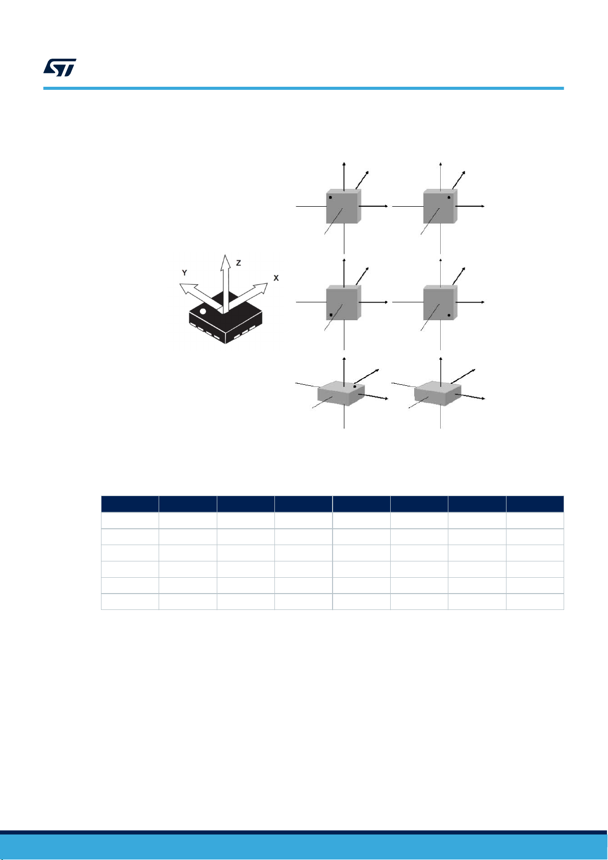
Figure 15. 6D recognized orientations
X
Y
Z
X
Y
Z
X
Y
Z
X
Y
Z
X
Y
Z
X
Y
Z
(a)
(c)
(e)
(b)
(d)
(f)
AN5398
6D/4D orientation detection
Table 30. D6D_SRC register in 6D positions
Case
(a) 1 0 0 1 0 0 0
(b) 1 0 0 0 0 0 1
(c) 1 0 0 0 0 1 0
(d) 1 0 0 0 1 0 0
(e) 1 1 0 0 0 0 0
(f) 1 0 1 0 0 0 0
D6D_IA ZH ZH YH YL XH XL
A basic SW routine for 6D orientation detection is as follows.
1.
Write 60h to CTRL1_XL // Turn on the accelerometer
2. Write 41h to TAP_CFG0 // Enable latch mode with reset on read
3. Write 80h to TAP_CFG2 // Enable interrupt function
4. Write 40h to TAP_THS_6D // Set 6D threshold (SIXD_THS[1:0] = 10b = 60 degrees)
5. Write 01h to CTRL8_XL // Enable LPF2 filter to 6D functionality
6. Write 04h to MD1_CFG // 6D interrupt driven to INT1 pin
// ODR_XL = 417 Hz, FS_XL = ±2 g
AN5398 - Rev 3
page 43/132
Page 44

5.4.2 4D orientation detection
The 4D direction function is a subset of the 6D function especially defined to be implemented in mobile devices
for portrait and landscape computation. It can be enabled by setting the D4D_EN bit of the TAP_THS_6D register
to 1. In this configuration, the Z-axis position detection is disabled, therefore reducing position recognition to
cases (a), (b), (c), and (d) of Table 30. D6D_SRC register in 6D positions.
5.5 Single-tap and double-tap recognition
The single-tap and double-tap recognition help to create a man-machine interface with little software loading. The
device can be configured to output an interrupt signal on a dedicated pin when tapped in any direction.
If the sensor is exposed to a single input stimulus, it generates an interrupt request on the inertial interrupt pin
INT1 and/or INT2. A more advanced feature allows the generation of an interrupt request when a double input
stimulus with programmable time between the two events is recognized, enabling a mouse button-like function.
The single-tap and double-tap recognition functions use the slope between two consecutive acceleration samples
to detect the tap events; the slope data is calculated using the following formula:
AN5398
Single-tap and double-tap recognition
slope(tn) = [ acc(tn) - acc(t
n-1
) ] / 2
This function can be fully programmed by the user in terms of expected amplitude and timing of the slope data by
means of a dedicated set of registers.
Single and double-tap recognition work independently of the selected output data rate. Recommended minimum
accelerometer ODR for these functions is 417 Hz.
In order to enable the single-tap and double-tap recognition functions it is necessary to set the
INTERRUPTS_ENABLE bit in TAP_CFG2 register to 1.
AN5398 - Rev 3
page 44/132
Page 45

5.5.1 Single tap
SHOCK
+ Tap Threshold
Interrupt
(a)
(b)
SHOCK
- Tap Threshold
Slope
If the device is configured for single-tap event detection, an interrupt is generated when the slope data of the
selected channel exceeds the programmed threshold, and returns below it within the Shock time window.
In the single-tap case, if the LIR bit of the TAP_CFG0 register is set to 0, the interrupt is kept active for
the duration of the Quiet window. If the LIR bit is set to 1, the interrupt is kept active until the TAP_SRC or
ALL_INT_SRC register is read.
The SINGLE_DOUBLE_TAP bit of WAKE_UP_THS has to be set to 0 in order to enable single-tap recognition
only.
In case (a) of Figure 16. Single-tap event recognition the single-tap event has been recognized, while in case (b)
the tap has not been recognized because the slope data falls below the threshold after the Shock time window
has expired.
AN5398
Single-tap and double-tap recognition
Figure 16. Single-tap event recognition
AN5398 - Rev 3
page 45/132
Page 46

5.5.2 Double tap
+ Tap Threshold
Interrupt
(a)
(b)
Interrupt
Slope
SHOCK
QUIET
DURATION
SHOCK
QUIET
DURATION
SHOCK
- Tap Threshold
QUIET
If the device is configured for double-tap event detection, an interrupt is generated when, after a first tap, a
second tap is recognized. The recognition of the second tap occurs only if the event satisfies the rules defined by
the Shock, the Quiet and the Duration time windows.
In particular, after the first tap has been recognized, the second tap detection procedure is delayed for an interval
defined by the Quiet time. This means that after the first tap has been recognized, the second tap detection
procedure starts only if the slope data exceeds the threshold after the Quiet window but before the Duration
window has expired. In case (a) of Figure 17 a double-tap event has been correctly recognized, while in case (b)
the interrupt has not been generated because the slope data exceeds the threshold after the window interval has
expired.
Once the second tap detection procedure is initiated, the second tap is recognized with the same rule as the first:
the slope data must return below the threshold before the Shock window has expired.
It is important to appropriately define the Quiet window to avoid unwanted taps due to spurious bouncing of the
input signal.
In the double-tap case, if the LIR bit of the TAP_CFG0 register is set to 0, the interrupt is kept active for
the duration of the Quiet window. If the LIR bit is set to 1, the interrupt is kept active until the TAP_SRC or
ALL_INT_SRC register is read.
AN5398
Single-tap and double-tap recognition
Figure 17. Double-tap event recognition (LIR bit = 0)
AN5398 - Rev 3
page 46/132
Page 47

5.5.3 Single-tap and double-tap recognition configuration
The device can be configured to output an interrupt signal when tapped (once or twice) in any direction: the
TAP_X_EN, TAP_Y_EN and TAP_Z_EN bits of the TAP_CFG0 register must be set to 1 to enable the tap
recognition on the X, Y, Z directions, respectively. In addition, the INTERRUPTS_ENABLE bit of the TAP_CFG2
register has to be set to 1.
Configurable parameters for tap recognition functionality are the tap thresholds (each axis has a dedicated
threshold) and the Shock, Quiet and Duration time windows.
The TAP_THS_X[4:0] bits of the TAP_CFG1 register, the TAP_THS_Y[4:0] bits of the TAP_CFG2 register and the
TAP_THS_Z[4:0] bits of the TAP_THS_6D register are used to select the unsigned threshold value used to detect
the tap event on the respective axis. The value of 1 LSB of these 5 bits depends on the selected accelerometer
full scale: 1 LSB = (FS_XL)/(25). The unsigned threshold is applied to both positive and negative slope data.
Both single-tap and double-tap recognition functions apply to only one axis. If more than one axis are enabled and
they are over the respective threshold, the algorithm continues to evaluate only the axis with highest priority. The
priority can be configured through the TAP_PRIORITY_[2:0] bits of TAP_CFG1. The following table shows all the
possible configurations.
Table 31. TAP_PRIORITY_[2:0] bits configuration
TAP_PRIORITY_[2:0] Maximum priority Middle priority Minimum priority
000 X Y Z
001 Y X Z
010 X Z Y
011 Z Y X
100 X Y Z
101 Y Z X
110 Z X Y
111 Z Y X
AN5398
Single-tap and double-tap recognition
The Shock time window defines the maximum duration of the overcoming threshold event: the acceleration must
return below the threshold before the Shock window has expired, otherwise the tap event is not detected. The
SHOCK[1:0] bits of the INT_DUR2 register are used to set the Shock time window value: the default value of
these bits is 00b and corresponds to 4/ODR_XL time, where ODR_XL is the accelerometer output data rate. If the
SHOCK[1:0] bits are set to a different value, 1 LSB corresponds to 8/ODR_XL time.
In the double-tap case, the Quiet time window defines the time after the first tap recognition in which there must
not be any overcoming threshold event. When latched mode is disabled (LIR bit of TAP_CFG is set to 0), the
Quiet time also defines the length of the interrupt pulse (in both single and double-tap case). The QUIET[1:0] bits
of the INT_DUR2 register are used to set the Quiet time window value: the default value of these bits is 00b and
corresponds to 2/ODR_XL time, where ODR_XL is the accelerometer output data rate. If the QUIET[1:0] bits are
set to a different value, 1 LSB corresponds to 4/ODR_XL time.
In the double-tap case, the Duration time window defines the maximum time between two consecutive detected
taps. The Duration time period starts just after the completion of the Quiet time of the first tap. The DUR[3:0] bits
of the INT_DUR2 register are used to set the Duration time window value: the default value of these bits is 0000b
and corresponds to 16/ODR_XL time, where ODR_XL is the accelerometer output data rate. If the DUR[3:0] bits
are set to a different value, 1 LSB corresponds to 32/ODR_XL time.
Figure 18. Single and double-tap recognition (LIR bit = 0) illustrates a single-tap event (a) and a double-tap event
(b). These interrupt signals can be driven to the two interrupt pins by setting to 1 the INT1_SINGLE_TAP bit of the
MD1_CFG register or the INT2_SINGLE_TAP bit of the MD2_CFG register for the single-tap case, and setting to
1 the INT1_DOUBLE_TAP bit of the MD1_CFG register or the INT2_DOUBLE_TAP bit of the MD2_CFG register
for the double-tap case.
No single/double-tap interrupt is generated if the accelerometer is in Inactivity status (see Section 5.6 Activity/
Inactivity and Motion/Stationary recognition for more details).
AN5398 - Rev 3
page 47/132
Page 48

+ Tap Threshold
(a)
(b)
Slope
- Tap Threshold
Interrupt
SHOCK
QUIET
DURATION
SHOCK
QUIET
Interrupt
QUIET
QUIET
SHOCK
SHOCK
SINGLE
TAP
DOUBLE
TAP
Single-tap and double-tap recognition
Figure 18. Single and double-tap recognition (LIR bit = 0)
AN5398
Tap interrupt signals can also be checked by reading the TAP_SRC (1Ch) register, described in the following
table.
Table 32. TAP_SRC register
b7
0 TAP_IA
b6 b5 b4 b3 b2 b1 b0
SINGLE
_TAP
DOUBLE
_TAP
TAP_
SIGN
X_TAP Y_TAP Z_TAP
• TAP_IA is set high when a single-tap or double-tap event has been detected.
• SINGLE_TAP is set high when a single tap has been detected.
• DOUBLE_TAP is set high when a double tap has been detected.
• TAP_SIGN indicates the acceleration sign when the tap event is detected. It is set low in case of positive
sign and it is set high in case of negative sign.
• X_TAP (Y_TAP, Z_TAP) is set high when the tap event has been detected on the X (Y, Z) axis.
Single and double-tap recognition works independently. Setting the SINGLE_DOUBLE_TAP bit of the
WAKE_UP_THS register to 0, only the single-tap recognition is enabled: double-tap recognition is disabled and
cannot be detected. When the SINGLE_DOUBLE_TAP is set to 1, both single and double-tap recognition are
enabled.
If latched mode is enabled and the interrupt signal is driven to the interrupt pins, the value assigned to
SINGLE_DOUBLE_TAP also affects the behavior of the interrupt signal: when it is set to 0, the latched mode
is applied to the single-tap interrupt signal; when it is set to 1, the latched mode is applied to the double-tap
interrupt signal only. The latched interrupt signal is kept active until the TAP_SRC or ALL_INT_SRC register is
read. The TAP_SIGN, X_TAP, Y_TAP, Z_TAP bits are maintained at the state in which the interrupt was generated
until the read is performed, and released at the next ODR cycle. In case the TAP_SIGN, X_TAP, Y_TAP, Z_TAP
bits have to be evaluated (in addition to the TAP_IA bit), it is recommended to directly read the TAP_SRC register
(do not use ALL_INT_SRC register for this specific case). If latched mode is enabled but the interrupt signal is not
driven to the interrupt pins, the latch feature does not take effect.
AN5398 - Rev 3
page 48/132
Page 49

5.5.4 Single-tap example
A basic SW routine for single-tap detection is given below.
1. Write 60h to CTRL1_XL // Turn on the accelerometer
2. Write 0Eh to TAP_CFG0 // Enable tap detection on X, Y, Z-axis
3. Write 09h to TAP_CFG1 // Set X-axis threshold and axes priority
4. Write 89h to TAP_CFG2 // Set Y-axis threshold and enable interrupt
5. Write 09h to TAP_THS_6D // Set Z-axis threshold
6. Write 06h to INT_DUR2 // Set Quiet and Shock time windows
7. Write 00h to WAKE_UP_THS // Only single-tap enabled (SINGLE_DOUBLE_TAP = 0)
8. Write 40h to MD1_CFG // Single-tap interrupt driven to INT1 pin
In this example the TAP_THS_X[4:0], TAP_THS_Y[4:0] and TAP_THS_Z[4:0] bits are set to 01001b, therefore the
tap threshold for each axis is 562.5 mg (= 9 * FS_XL / 25).
The SHOCK field of the INT_DUR2 register is set to 10b: an interrupt is generated when the slope data exceeds
the programmed threshold, and returns below it within 38.5 ms (= 2 * 8 / ODR_XL) corresponding to the Shock
time window.
The QUIET field of the INT_DUR2 register is set to 01b: since latched mode is disabled, the interrupt is kept high
for the duration of the Quiet window, therefore 9.6 ms (= 1 * 4 / ODR_XL).
AN5398
Single-tap and double-tap recognition
// ODR_XL = 417 Hz, FS_XL = ±2 g
5.5.5 Double-tap example
A basic SW routine for double-tap detection is given below.
1. Write 60h to CTRL1_XL // Turn on the accelerometer
2. Write 0Eh to TAP_CFG0 // Enable tap detection on X, Y, Z-axis
3. Write 0Ch to TAP_CFG1 // Set X-axis threshold and axes priority
4. Write 8Ch to TAP_CFG2 // Set Y-axis threshold and enable interrupt
5. Write 0Ch to TAP_THS_6D // Set Z-axis threshold
6. Write 7Fh to INT_DUR2 // Set Duration, Quiet and Shock time windows
7. Write 80h to WAKE_UP_THS // Single-tap and double-tap enabled (SINGLE_DOUBLE_TAP = 1)
8. Write 08h to MD1_CFG // Double-tap interrupt driven to INT1 pin
In this example the TAP_THS_X[4:0], TAP_THS_Y[4:0] and TAP_THS_Z[4:0] bits are set to 01100b, therefore the
tap threshold is 750 mg (= 12 * FS_XL / 25).
For interrupt generation, during the first and the second tap the slope data must return below the threshold before
the Shock window has expired. The SHOCK field of the INT_DUR2 register is set to 11b, therefore the Shock time
is 57.7 ms (= 3 * 8 / ODR_XL).
For interrupt generation, after the first tap recognition there must not be any slope data overthreshold during the
Quiet time window. Furthermore, since latched mode is disabled, the interrupt is kept high for the duration of
the Quiet window. The QUIET field of the INT_DUR2 register is set to 11b, therefore the Quiet time is 28.8 ms
(= 3 * 4 / ODR_XL).
For the maximum time between two consecutive detected taps, the DUR field of the INT_DUR2 register is set to
0111b, therefore the Duration time is 538.5 ms (= 7 * 32 / ODR_XL).
// ODR_XL = 417 Hz, FS_XL = ±2 g
AN5398 - Rev 3
page 49/132
Page 50

Activity/Inactivity and Motion/Stationary recognition
5.6 Activity/Inactivity and Motion/Stationary recognition
The working principle of Activity/Inactivity and Motion/Stationary embedded functions is similar to wake-up. If no
movement condition is detected for a programmable time, an inactivity/stationary condition event is generated;
otherwise, when the accelerometer data exceed the configurable threshold, an Activity/Motion condition event is
generated.
The Activity/Inactivity recognition function allows reducing system power consumption and developing new smart
applications.
When the Activity/Inactivity recognition function is activated, the device is able to automatically decrease the
accelerometer sampling rate to 12.5 Hz (Low-Power mode) and to automatically increase the accelerometer ODR
and bandwidth as soon as the wake-up interrupt event has been detected. This feature can be extended to the
gyroscope, with three possible options:
• Gyroscope configurations do not change;
• Gyroscope enters in Sleep mode;
• Gyroscope enters in Power-Down mode.
With this feature the system may be efficiently switched from low-power consumption to full performance and
vice-versa depending on user-selectable acceleration events, thus ensuring power saving and flexibility.
The Activity/Inactivity recognition function is enabled by setting the INTERRUPTS_ENABLE bit to 1 and
configuring the INACT_EN[1:0] bits of the TAP_CFG2 register. If the INACT_EN[1:0] bits of the TAP_CFG2
register are equal to 00b, the Motion/Stationary embedded function is enabled. Possible configurations of the
inactivity event are summarized in the following table.
AN5398
Table 33. Inactivity event configuration
INACT_EN[1:0]
00 Inactivity event disabled Inactivity event disabled
01 XL ODR = 12.5 Hz (Low-Power mode) Gyro configuration unchanged
10 XL ODR = 12.5 Hz (Low-Power mode) Gyro in Sleep mode
11 XL ODR = 12.5 Hz (Low-Power mode) Gyro in Power-Down mode
Accelerometer Gyroscope
The Activity/Inactivity and Motion/Stationary recognition functions can be implemented using either the slope filter
(see Section 3.7.1 Accelerometer slope filter for more details) or the high-pass digital filter, as illustrated in
Figure 2. Accelerometer filtering chain (UI path). The filter to be applied can be selected using the SLOPE_FDS
bit of the TAP_CFG0 register: if this bit is set to 0 (default value), the slope filter is used; if it is set to 1, the
high-pass digital filter is used.
This function can be fully programmed by the user in terms of expected amplitude and timing of the filtered data
by means of a dedicated set of registers (Figure 19. Activity/Inactivity recognition (using the slope filter)).
The unsigned threshold value is defined using the WK_THS[5:0] bits of the WAKE_UP_THS register; the value of
1 LSB of these 6 bits depends on the selected accelerometer full scale and on the value of the WAKE_THS_W bit
of the WAKE_UP_DUR register:
• if WAKE_THS_W = 0, 1 LSB = FS_XL / 26;
• if WAKE_THS_W = 1, 1 LSB = FS_XL / 28.
The threshold is applied to both positive and negative filtered data.
When a certain number of consecutive X,Y,Z filtered data is smaller than the configured threshold, the
ODR_XL[3:0] bits of the CTRL1_XL register are bypassed (Inactivity) and the accelerometer is internally set
to 12.5 Hz although the content of CTRL1_XL is left untouched. The gyroscope behavior varies according to
the configuration of the INACT_EN[1:0] bits of the TAP_CFG2 register. The duration of the Inactivity status to
be recognized is defined by the SLEEP_DUR[3:0] bits of the WAKE_UP_DUR register: 1 LSB corresponds to
512/ODR_XL time, where ODR_XL is the accelerometer output data rate. If the SLEEP_DUR[3:0] bits are set to
0000b, the duration of the Inactivity status to be recognized is equal to 16 / ODR_XL time.
When the Inactivity status is detected, the interrupt is set high for 1/ODR_XL[s] period then it is automatically
deasserted.
AN5398 - Rev 3
page 50/132
Page 51

Interrupt
Slope
SLEEP_DUR
INACTIVITY
STATUS
+ WK Threshold
ACTIVITY
STATUS
- WK Threshold
ACTIVITY
STATUS
AN5398
Activity/Inactivity and Motion/Stationary recognition
When filtered data on one axis becomes bigger than the threshold for a configurable time, the CTRL1_XL register
settings are immediately restored (Activity) and the gyroscope is restored to the previous state. The duration of
the Activity status to be recognize is defined by the WAKE_DUR[1:0] bits of the WAKE_UP_DUR register. 1 LSB
corresponds to 1 / ODR_XL time, where ODR_XL is the accelerometer output data rate.
When the Activity status is detected, the interrupt is set high for 1/ODR_XL[s] period then it is automatically
deasserted.
Once the Activity/Inactivity detection function is enabled, the status can be driven to the two interrupt pins by
setting to 1 the INT1_SLEEP_CHANGE bit of the MD1_CFG register or the INT2_SLEEP_CHANGE bit of the
MD2_CFG register; it can also be checked by reading the SLEEP_CHANGE_IA bit of the WAKE_UP_SRC or
ALL_INT_SRC register.
The SLEEP_CHANGE_IA bit is by default in pulsed mode. Latched mode can be selected by setting the
LIR bit of the TAP_CFG0 register to 1 and the the INT1_SLEEP_CHANGE of the MD1_CFG register or
INT2_SLEEP_CHANGE of the MD2_CFG register to 1. The SLEEP_STATE bit of the WAKE_UP_SRC register is
not affected by the LIR configuration: it corresponds to the current state of the device when the WAKE_UP_SRC
register is read.
By setting the SLEEP_STATUS_ON_INT bit of the TAP_CFG0 register to 1, the signal routed to the INT1 or INT2
pins is configured to be the Activity/Inactivity state (SLEEP_STATE bit of WAKE_UP_SRC register) instead of the
sleep-change signal: it goes high during Inactivity state and it goes low during Activity state. Latched mode is not
supported in this configuration.
Figure 19. Activity/Inactivity recognition (using the slope filter)
AN5398 - Rev 3
page 51/132
Page 52

Activity/Inactivity and Motion/Stationary recognition
A basic SW routine for Activity/Inactivity detection is as follows:
1. Write 50h to CTRL1_XL // Turn on the accelerometer
// ODR_XL = 208 Hz, FS_XL = ±2 g
2. Write 40h to CTRL2_G // Turn on the gyroscope
// ODR_G = 104 Hz, FS_G = ±250 dps
3. Write 02h to WAKE_UP_DUR // Set duration for Inactivity detection
// Select Activity/Inactivity threshold resolution and duration
4. Write 02h to WAKE_UP_THS // Set Activity/Inactivity threshold
5. Write 00h to TAP_CFG0 // Select sleep-change notification
// Select slope filter
6. Write E0h to TAP_CFG2 // Enable interrupt
// Inactivity configuration: accelerometer to 12.5 Hz (LP mode),
// Gyroscope to Power-Down mode
7. Write 80h to MD1_CFG // Activity/Inactivity interrupt driven to INT1 pin
AN5398
In this example the WK_THS field of the WAKE_UP_THS register is set to 000010b, therefore the Activity/
Inactivity threshold is 62.5 mg (= 2 * FS_XL / 26 since the WAKE_THS_W bit of the WAKE_UP_DUR register is
set to 0).
Before Inactivity detection, the X,Y,Z slope data must be smaller than the configured threshold for a period of
time defined by the SLEEP_DUR field of the WAKE_UP_DUR register: this field is set to 0010b, corresponding
to 4.92 s (= 2 * 512 / ODR_XL). After this period of time has elapsed, the accelerometer ODR is internally set to
12.5 Hz and the gyroscope is internally set to Power-Down mode.
The Activity status is detected and the CTRL1_XL register settings are immediately restored and the gyroscope is
turned on as soon as the slope data of (at least) one axis are bigger than the threshold for one sample, since the
WAKE_DUR[1:0] bits of the WAKE_UP_DUR register are configured to 00b.
5.6.1 Stationary/Motion detection
Stationary/Motion detection is a particular case of the Activity/Inactivity functionality in which no ODR / power
mode changes occur when a sleep condition (equivalent to Stationary condition) is detected. Stationary/Motion
detection is activated by setting the INACT_EN[1:0] bits of the TAP_CFG2 register to 00b.
AN5398 - Rev 3
page 52/132
Page 53

5.7 Boot status
After the device is powered up, it performs a 10 ms (maximum) boot procedure to load the trimming parameters.
After the boot is completed, both the accelerometer and the gyroscope are automatically configured in PowerDown mode. During the boot time the registers are not accessible.
After power up, the trimming parameters can be re-loaded by setting the BOOT bit of the CTRL3_C register to 1.
No toggle of the device power lines is required and the content of the device control registers is not modified, so
the device operating mode doesn’t change after boot. If the reset to the default value of the control registers is
required, it can be performed by setting the SW_RESET bit of the CTRL3_C register to 1. When this bit is set
to 1, the following registers are reset to their default value:
• FUNC_CFG_ACCESS (01h);
• PIN_CTRL (02h);
• FIFO_CTRL1 (07h) through FIFO_CTRL4 (0Ah);
• COUNTER_BDR_REG1 (0Bh) and COUNTER_BDR_REG2 (0Ch);
• INT1_CTRL (0Dh) and INT2_CTRL (0Eh);
• CTRL1_XL (10h) through CTRL10_C (19h);
• FIFO_STATUS1 (3Ah) and FIFO_STATUS2 (3Bh);
• TAP_CFG0 (56h) through MD2_CFG (5Fh);
• X_OFS_USR (73h), Y_OFS_USR (74h) and Z_OFS_USR (75h).
The SW_RESET procedure can take 50 µs; the status of reset is signaled by the status of the SW_RESET bit of
the CTRL3_C register: once the reset is completed, this bit is automatically set low.
The boot status signal is driven to the INT1 interrupt pin by setting the INT1_BOOT bit of the INT1_CTRL register
to 1: this signal is set high while the boot is running and it is set low again at the end of the boot procedure.
The reboot flow is as follows:
1. Set both accelerometer and gyroscope in Power-Down mode;
2. Set INT1_BOOT bit of INT1_CTRL register to 1 [optional];
3. Set BOOT bit of CTRL3_C register to 1;
4. Monitor reboot status, three possibilities:
a. Wait 10 ms;
b. Monitor INT1 pin until it returns to 0 (step 2. is mandatory in this case);
c. Poll BOOT bit of CTRL3_C until it returns to 0.
Reset flow is as follows:
1. Set both accelerometer and gyroscope in in Power-down mode;
2. Set to 1 the SW_RESET bit of CTRL3_C to 1;
3. Monitor software reset status, two possibilities:
a. Wait 50 µs
b. Poll SW_RESET bit of CTRL3_C until it returns to 0.
In order to avoid conflicts, the reboot and the sw reset must not be executed at the same time (do not set to 1 at
the same time both the BOOT bit and SW_RESET bit of CTRL3_C register). The above flows must be performed
serially.
AN5398
Boot status
AN5398 - Rev 3
page 53/132
Page 54

6 Embedded functions
The device implements in hardware many embedded functions; specific IP blocks with negligible power
consumption and high-level performance implement the following functions:
• Pedometer functions (step detector and step counter);
• Significant motion;
• Relative tilt;
• Timestamp.
6.1 Pedometer functions: step detector and step counter
A specific IP block is dedicated to pedometer functions: the step detector and the step counter.
Pedometer functions work at 26 Hz and are based on the accelerometer sensor only; consequently, the
accelerometer ODR must be set at a value of 26 Hz or higher when using them.
In order to enable the pedometer functions it is necessary to set the PEDO_EN bit of the EMB_FUNC_EN_A
embedded functions register to 1. The algorithm internal state can be re-initialized by asserting the
STEP_DET_INIT bit of the EMB_FUNC_INIT_A embedded functions register.
The step counter indicates the number of steps detected by the step detector algorithm after the pedometer
function has been enabled. The step count is given by the concatenation of the STEP_COUNTER_H and
STEP_COUNTER_L embedded functions registers and it is represented as a 16-bit unsigned number.
The step count is not reset to zero when the accelerometer is configured in Power-Down or the pedometer is
disabled or re-initialized; it can be reset to zero by setting the PEDO_RST_STEP bit of the EMB_FUNC_SRC
register to 1. After the counter resets, the PEDO_RST_STEP bit is automatically set back to 0.
The step detector functionality generates an interrupt every time a step is recognized. In case of interspersed step
sessions, 10 consecutive steps (debounce steps) have to be detected before the first interrupt generation in order
to avoid false step detections (debounce functionality).
The number of debounce steps can be modified through the DEB_STEP[7:0] bits of the
PEDO_DEB_STEPS_CONF register in the embedded advanced features registers: basically, it corresponds
to the minimum number of steps to be detected before the first step counter increment. 1 LSB of this field
corresponds to 1 step, the default value is 10 steps. The debounce functionality restarts after around 1.2 s of
device inactivity.
STMicroelectronics provides the tools to generate specific pedometer configurations starting from a set of data
logs with a reference number of steps (Unico GUI on st.com).
The EMB_FUNC_SRC embedded functions register contains some read-only bits related to the pedometer
function state.
AN5398
Embedded functions
AN5398 - Rev 3
Table 34. EMB_FUNC_SRC embedded functions register
b7
PEDO_RST
_STEP
b6 b5 b4 b3 b2 b1 b0
0
STEP_
DETECTED
STEP_COUNT
_DELTA_IA
STEP_
OVERFLOW
STEPCOUNTER
_BIT_SET
0 0
• PEDO_RST_STEP: pedometer step counter reset. It can be set to 1 to reset the number of steps counted. It
is automatically set back to 0 after the counter reset.
• STEP_DETECTED: step detector event status. It signals a step detection (after the debounce).
• STEP_COUNT_DELTA_IA: instead of generating an interrupt signal every time a step is recognized, it is
possible to generate it if at least one step is detected within a certain time period, defined by setting a
value different from 00h in the in PEDO_SC_DELTAT_H and PEDO_SC_DELTAT_L embedded advanced
features (page 1) registers. It is necessary to set the TIMESTAMP_EN bit of the CTRL10_C register
to 1 (to enable the timer). The time period is given by the concatenation of PEDO_SC_DELTAT_H
and PEDO_SC_DELTAT_L and it is represented as a 16-bit unsigned value with a resolution of 6.4
ms. STEP_COUNT_DELTA_IA goes high (at the end of each time period) if at least one step is
counted (after the debounce) within the programmed time period. If the time period is not programmed
(PEDO_SC_DELTAT = 0), this bit is kept to 0.
page 54/132
Page 55

AN5398
Pedometer functions: step detector and step counter
• STEP_OVERFLOW: overflow signal which goes high when the step counter value reaches 216.
• STEPCOUNTER_BIT_SET: step counter event status. It signals an increase in the step counter (after
the debounce). If a timer period is programmed in the PEDO_SC_DELTAT_H and PEDO_SC_DELTAT_L
embedded advanced features (page 1) registers, this bit is kept to 0.
The step detection interrupt signal can also be checked by reading the IS_STEP_DET bit
of the EMB_FUNC_STATUS embedded functions register or the IS_STEP_DET bit of the
EMB_FUNC_STATUS_MAINPAGE register.
The IS_STEP_DET bit can have different behaviors, as summarized in the table below, depending on the value of
the PEDO_SC_DELTAT bit in the EMB_FUNC_SRC embedded functions register and the CARRY_COUNT_EN
bit in the PEDO_CMD_REG embedded advanced features register.
Table 35. IS_STEP_DET configuration
PEDO_SC_DELTAT CARRY_COUNT_EN IS_STEP_DET
PEDO_SC_DELTAT = 0 0 STEPCOUNTER_BIT_SET
PEDO_SC_DELTAT > 0 0 STEP_COUNT_DELTA_IA
PEDO_SC_DELTAT ≥ 0 1 STEP_OVERFLOW
The IS_STEP_DET interrupt signal can be driven to the INT1/INT2 interrupt pin by setting the
INT1_STEP_DETECTOR/INT2_STEP_DETECTOR bit of the EMB_FUNC_INT1/EMB_FUNC_INT2 register to 1.
In this case it is mandatory to also enable the embedded functions event routing to the INT1/INT2 interrupt pin by
setting the INT1_EMB_FUNC/INT2_EMB_FUNC bit of the MD1_CFG/MD2_CFG register.
The behavior of the interrupt signal is pulsed by default. The duration of the pulse is equal to 1/26 Hz. Latched
mode can be enabled by setting the EMB_FUNC_LIR bit of the PAGE_RW embedded functions register to 1. In
this case, the interrupt signal is reset by reading the IS_STEP_DET bit of the EMB_FUNC_STATUS embedded
functions register or the IS_STEP_DET bit of the EMB_FUNC_STATUS_MAINPAGE register.
The step counter can be batched in FIFO (see Section 9 First-in, first-out (FIFO) buffer for details).
A basic SW routine which shows how to enable step counter detection is as follows:
1.
Write 80h to FUNC_CFG_ACCESS // Enable access to embedded functions registers
2. Write 08h to EMB_FUNC_EN_A // Enable pedometer
3. Write 08h to EMB_FUNC_INT1 // Step detection interrupt driven to INT1 pin
4. Write 00h to FUNC_CFG_ACCESS // Disable access to embedded functions registers
5. Write 02h to MD1_CFG // Enable embedded functions interrupt routing
6. Write 28h to CTRL1_XL // Turn on the accelerometer - ODR_XL = 26 Hz, FS_XL = ±4 g
AN5398 - Rev 3
page 55/132
Page 56

6.2 Significant motion
The significant motion function generates an interrupt when a ‘significant motion’, that could be due to a change
in user location, is detected. In the device this function has been implemented in hardware using only the
accelerometer.
The significant motion functionality can be used in location-based applications in order to receive a notification
indicating when the user is changing location.
The significant motion function works at 26 Hz, so the accelerometer ODR must be set at a value of 26 Hz or
higher. It generates an interrupt when the difference between the number of steps counted from its initialization/
reset is higher than 10 steps. After an interrupt generation, the algorithm internal state is reset.
In order to enable significant motion detection it is necessary to set the SIGN_MOTION_EN bit of the
EMB_FUNC_EN_A embedded functions register to 1. The algorithm can be re-initialized by asserting the
SIG_MOT_INIT bit of the EMB_FUNC_INIT_A embedded functions register.
Note: The significant motion feature automatically enables the internal step counter algorithm.
The significant motion interrupt signal can be driven to the INT1/INT2 interrupt pin by setting the INT1_SIG_MOT/
INT2_SIG_MOT bit of the EMB_FUNC_INT1/EMB_FUNC_INT2 register to 1. In this case it is mandatory to
also enable the embedded functions event routing to the INT1/INT2 interrupt pin by setting the INT1_EMB_FUNC/
INT2_EMB_FUNC bit of the MD1_CFG/MD2_CFG register.
The significant motion interrupt signal can also be checked by reading the IS_SIGMOT
bit of the EMB_FUNC_STATUS embedded functions register or the IS_SIGMOT bit of the
EMB_FUNC_STATUS_MAINPAGE register.
The behavior of the significant motion interrupt signal is pulsed by default. The duration of the pulse is equal to
1/26 Hz. Latched mode can be enabled by setting the EMB_FUNC_LIR bit of the PAGE_RW embedded functions
register to 1: in this case, the interrupt signal is reset by reading the IS_SIGMOT bit of the EMB_FUNC_STATUS
embedded functions register or the IS_SIGMOT bit of the EMB_FUNC_STATUS_MAINPAGE register.
A basic SW routine which shows how to enable significant motion detection is as follows:
AN5398
Significant motion
1.
Write 80h to FUNC_CFG_ACCESS // Enable access to embedded functions registers
2. Write 20h to EMB_FUNC_EN_A // Enable significant motion detection
3. Write 20h to EMB_FUNC_INT1 // Significant motion interrupt driven to INT1 pin
4. Write 80h to PAGE_RW // Enable latched mode for embedded functions
5. Write 00h to FUNC_CFG_ACCESS // Disable access to embedded functions registers
6. Write 02h to MD1_CFG // Enable embedded functions interrupt routing
7. Write 20h to CTRL1_XL // Turn on the accelerometer
// ODR_XL = 26 Hz, FS_XL = ±2 g
AN5398 - Rev 3
page 56/132
Page 57
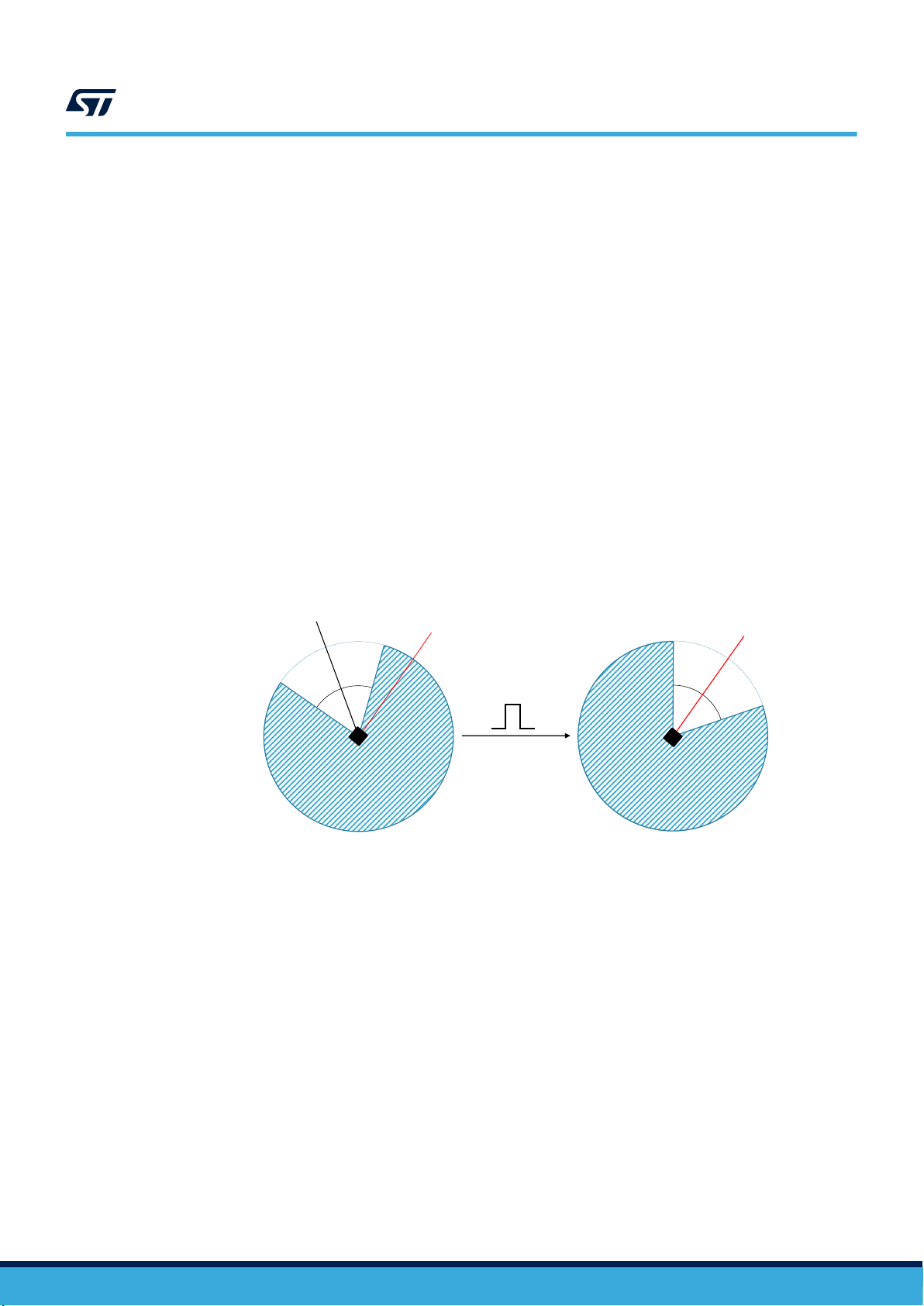
6.3 Relative tilt
35º
35º
START
POSITION
#0
FINAL
POSITION
#0
35º
START
POSITION
#1
35º
TILT
DETECTION
INTERRUPT
The tilt function allows detecting when an activity change occurs (e.g. when phone is in a front pocket and the
user goes from sitting to standing or from standing to sitting). In the device it has been implemented in hardware
using only the accelerometer.
The tilt function works at 26 Hz, so the accelerometer ODR must be set at a value of 26 Hz or higher.
In order to enable the relative tilt detection function it is necessary to set the TILT_EN bit of the
EMB_FUNC_EN_A embedded functions register to 1. The algorithm can be re-initialized by asserting the
TILT_INIT bit of the EMB_FUNC_INIT_A embedded functions register.
If the device is configured for tilt event detection, an interrupt is generated when the device is tilted by an angle
greater than 35 degrees from the start position. The start position is defined as the position of the device when the
tilt detection is enabled/re-initialized or the position of the device when the last tilt interrupt was generated.
After this function is enabled or re-initialized, the tilt logic typically requires a 2-second settling time before being
able to generate the first interrupt.
In the example shown in Figure 20 tilt detection is enabled when the device orientation corresponds to “start
position #0”. The first interrupt is generated if the device is rotated by an angle greater than 35 degrees from
the start position. After the first tilt detection interrupt is generated, the new start position (#1) corresponds to the
position of the device when the previous interrupt was generated (final position #0), and the next interrupt signal
will be generated as soon as the device is tilted by an angle greater than 35 degrees, entering the blue zone
surrounding the start position #1.
AN5398
Relative tilt
Figure 20. Tilt example
AN5398 - Rev 3
The tilt interrupt signal can be driven to the INT1/INT2 interrupt pin by setting the INT1_TILT/INT2_TILT bit of
the EMB_FUNC_INT1/EMB_FUNC_INT2 register to 1. In this case it is mandatory to also enable the embedded
functions event routing to the INT1/INT2 interrupt pin by setting the INT1_EMB_FUNC/INT2_EMB_FUNC bit of
MD1_CFG/MD2_CFG register.
The tilt interrupt signal can also be checked by reading the IS_TILT bit of the EMB_FUNC_STATUS embedded
functions register or the IS_TILT bit of the EMB_FUNC_STATUS_MAINPAGE register.
The behavior of the tilt interrupt signal is pulsed by default. The duration of the pulse is equal to 1/26 Hz. Latched
mode can be enabled by setting the EMB_FUNC_LIR bit of the PAGE_RW embedded functions register to 1. In
this case, the interrupt signal is reset by reading the IS_TILT bit of the EMB_FUNC_STATUS embedded functions
register or the IS_TILT bit of the EMB_FUNC_STATUS_MAINPAGE register.
page 57/132
Page 58

Hereafter a basic SW routine which shows how to enable the tilt detection function:
1. Write 80h to FUNC_CFG_ACCESS // Enable access to embedded functions registers
2. Write 10h to EMB_FUNC_EN_A // Enable tilt detection
3. Write 10h to EMB_FUNC_INT1 // Tilt interrupt driven to INT1 pin
4. Write 80h to PAGE_RW // Enable latched mode for embedded functions
5. Write 00h to FUNC_CFG_ACCESS // Disable access to embedded functions registers
6. Write 02h to MD1_CFG // Enable embedded functions interrupt routing
7. Write 20h to CTRL1_XL // Turn on the accelerometer
// ODR_XL = 26 Hz, FS_XL = ±2 g
AN5398
Relative tilt
AN5398 - Rev 3
page 58/132
Page 59

6.4 Timestamp
Together with sensor data the device can provide timestamp information.
To enable this functionality the TIMESTAMP_EN bit of the CTRL10_C register has to be set to 1. The time step
count is given by the concatenation of the TIMESTAMP3 & TIMESTAMP2 & TIMESTAMP1 & TIMESTAMP0
registers and is represented as a 32-bit unsigned number.
The nominal timestamp resolution is 25 μs. It is possible to get the actual timestamp resolution value through the
FREQ_FINE[7:0] bits of the INTERNAL_FREQ_FINE register, which contains the difference in percentage of the
actual ODR (and timestamp rate) with respect to the nominal value.
Similarly, it is possible to get the actual output data rate by using the following formula:
where the ODR
t
s =
actual
ODR
actual
values are indicated in the table below.
coeff
40000 ⋅
Hz =
1
1 + 0.0015 ⋅ FREQ_FINE
6667 + 0.0015 ⋅ FREQ_FINE ⋅ 6667
ODR
coeff
AN5398
Timestamp
Table 36. ODR
Selected ODR [Hz]
12.5 512
26 256
52 128
104 64
208 32
417 16
833 8
1667 4
3333 2
6667 1
coeff
values
ODR
coeff
If both the accelerometer and the gyroscope are in Power-Down mode, the timestamp counter does not work and
the timestamp value is frozen at the last value.
When the maximum value 4294967295 LSB (equal to FFFFFFFFh) is reached corresponding to approximately 30
hours, the counter is automatically reset to 00000000h and continues to count. The timer count can be reset to
zero at any time by writing the reset value AAh in the TIMESTAMP2 register.
The TIMESTAMP_ENDCOUNT bit of the ALL_INT_SRC goes high 6.4 ms before the occurrence of a timestamp
overrun condition. This flag is reset when the ALL_INT_SRC register is read. It is also possible to route this signal
on the INT2 pin (75 μs duration pulse) by setting the INT2_TIMESTAMP bit of MD2_CFG to 1.
The timestamp can be batched in FIFO (see Section 9 First-in, first-out (FIFO) buffer for details).
AN5398 - Rev 3
page 59/132
Page 60

7 Mode 2 - Sensor hub mode
DEVICE
Ext Sensor
SDx
SCx
INT2
SDA
SCL
Data Ready
I
C MASTER I
C SLAVE
External trigger is optional
R
Vdd_IO
R
Vdd_IO
External pull-up is optional
2
2
The hardware flexibility of the ISM330DHCX allows connecting the pins with different mode connections to
external sensors to expand functionalities such as adding a sensor hub. When sensor hub mode (Mode 2) is
enabled, both the primary I²C/SPI (3- and 4-wire) slave interface and the I²C master interface for the connection of
external sensors are available. Mode 2 connection mode is described in detail in the following paragraphs.
7.1 Sensor hub mode description
In sensor hub mode (Mode 2) up to 4 external sensors can be connected to the I²C master interface of the device.
The sensor hub trigger signal can be synchronized with the accelerometer/gyroscope data-ready signal (up to
104 Hz). In this configuration, the sensor hub ODR can be configured through the SHUB_ODR_[1:0] bits of the
SLAVE0_CONFIG register. Alternatively, an external signal connected to the INT2 pin can be used as the sensor
hub trigger. In this second case, the maximum ODR supported for external sensors depends on the number of
read / write operations that can be executed between two consecutive trigger signals.
On the sensor hub trigger signal, all the write and read I²C operations configured through the registers
SLVx_ADD, SLVx_SUBADD, SLAVEx_CONFIG and DATAWRITE_SLV0 are performed sequentially from external
sensor 0 to external sensor 3 (depending on the external sensors enabled through the AUX_SENS_ON[1:0] field
in the MASTER_CONFIG register).
External sensor data can also be stored in FIFO (see Section 9 First-in, first-out (FIFO) buffer for details).
If both the accelerometer and the gyroscope are in Power-Down mode, the sensor hub does not work.
All external sensors have to be connected in parallel to the SDx/SCx pins of the device, as illustrated in
Figure 21. External sensor connections in Mode 2 for a single external sensor. External pull-up resistors and
the external trigger signal connection are optional and depend on the configuration of the registers.
AN5398
Mode 2 - Sensor hub mode
Figure 21. External sensor connections in Mode 2
AN5398 - Rev 3
page 60/132
Page 61

7.2 Sensor hub mode registers
The sensor hub configuration registers and output registers are accessible when the bit SHUB_REG_ACCESS
of the FUNC_CFG_ACCESS register is set to 1. After setting the SHUB_REG_ACESS bit to 1, only sensor hub
registers are available. In order to guarantee the correct register mapping for other operations, after the sensor
hub configuration or output data reading, the SHUB_REG_ACCESS bit of the FUNC_CFG_ACCESS register
must be set to 0.
The MASTER_CONFIG register has to be used for the configuration of the I²C master interface.
A set of registers SLVx_ADD, SLVx_SUBADD, SLAVEx_CONFIG is dedicated to the configuration of the 4
slave interfaces associated to the 4 connectable external sensors. An additional register, DATAWRITE_SLV0, is
associated to slave #0 only. It has to be used to implement the write operations.
Finally, 18 registers (from SENSOR_HUB_1 to SENSOR_HUB_18) are available to store the data read from the
external sensors.
7.2.1 MASTER_CONFIG (14h)
This register is used to configure the I²C master interface.
b7 b6 b5 b4 b3 b2 b1 b0
RST_
MASTER_REGS
WRITE_
ONCE
START_
CONFIG
Table 37. MASTER_CONFIG register
PASS_THROUGH
_MODE
SHUB_
PU_EN
MASTER_ON
AN5398
Sensor hub mode registers
AUX_
SENS_ON1
AUX_
SENS_ON0
• RST_MASTER_REGS bit is used to reset the I²C master interface, configuration and output registers. It
must be manually asserted and de-asserted.
• WRITE_ONCE bit is used to limit the write operations on slave 0 to only one occurrence (avoiding to repeat
the same write operation multiple times). If this bit is not asserted, a write operation is triggered at each
ODR.
Note: The WRITE_ONCE bit must be set to 1 if the slave 0 is used for reading.
• START_CONFIG bit selects the sensor hub trigger signal.
– When this bit is set to 0, the accelerometer/gyroscope sensor has to be active (not in Power-Down
mode) and the sensor hub trigger signal is the accelerometer/gyroscope data-ready signal, with a
frequency defined by the SHUB_ODR_[1:0] bits of the SLAVE0_CONFIG register (up to 104 Hz).
– When this bit is set to 1, at least one sensor between the accelerometer and the gyroscope has to
be active and the sensor hub trigger signal is the INT2 pin. In fact, when both the MASTER_ON bit
and START_CONFIG bit are set to 1, the INT2 pin is configured as an input signal. In this case, the
INT2 pin has to be connected to the data-ready pin of the external sensor (Figure 21. External sensor
connections in Mode 2) in order to trigger the read/write operations on the external sensor registers.
Sensor hub interrupt from INT2 is ‘high-level triggered’ (not programmable).
Note: In case of external trigger signal usage (START_CONFIG=1), if the INT2 pin is connected to the
data-ready pin of the external sensor (Figure 21. External sensor connections in Mode 2) and the latter is
in Power-Down mode, then no data-ready signal can be generated by the external sensor. For this reason,
the initial configuration of the external sensor’s register has to be performed using the internal trigger signal
(START_CONFIG=0). After the external sensor is activated and the data-ready signal is available, the
external trigger signal can be used by switching the START_CONFIG bit to 1.
• PASS_THROUGH_MODE bit is used to enable/disable the I²C interface pass-through. When this bit is set
to 1, the main I²C line (e.g. connected to an external microcontroller) is short-circuited with the auxiliary
one, in order to implement a direct access to the external sensor registers. See Section 7.3 Sensor hub
pass-through feature for details.
• SHUB_PU_EN bit enables/disables the internal pull-up on the I²C master line. When this bit is set to 0, the
internal pull-up is disabled and the external pull-up resistors on the SDx/SCx pins are required, as shown in
Figure 21. External sensor connections in Mode 2. When this bit is set to 1, the internal pull-up is enabled
(regardless of the configuration of the MASTER_ON bit) and the external pull-up resistors on the SDx/SCx
pins are not required.
AN5398 - Rev 3
page 61/132
Page 62

• MASTER_ON bit has to be set to 1 to enable the auxiliary I²C master of the device (sensor hub mode). In
order to change the sensor hub configuration at runtime or when setting the accelerometer and gyroscope
sensor in Power-Down mode, or when applying the software reset procedure, the I²C master must be
disabled, followed by a 300 µs wait. The following procedure must be implemented:
1. Turn off I²C master by setting MASTER_ON = 0.
2. Wait 300 µs.
3. Change the configuration of the sensor hub registers or set the accelerometer/gyroscope in Power-Down
mode or apply the software reset procedure.
• AUX_SENS_ON[1:0] bits have to be set accordingly to the number of slaves to be used. I²C transactions are
performed sequentially from slave 0 to slave 3. The possible values are:
– 00b: one slave;
– 01b: two slaves;
– 10b: three slaves;
– 11b: four slaves.
7.2.2 STATUS_MASTER (22h)
The STATUS_MASTER register, similarly to the other sensor hub configurations and output registers, can
be read only after setting the SHUB_REG_ACCESS bit of the FUNC_CFG_ACCESS register to 1. The
STATUS_MASTER register is also mapped to the STATUS_MASTER_MAINPAGE register, which can be directly
read without enabling access to the sensor hub registers.
AN5398
Sensor hub mode registers
Table 38. STATUS_MASTER / STATUS_MASTER_MAINPAGE register
b7 b6 b5 b4 b3 b2 b1 b0
WR_ONCE
_DONE
SLAVE3_
NACK
SLAVE2_
NACK
SLAVE1_
NACK
SLAVE0_
NACK
0 0
SENS_HUB_
ENDOP
• WR_ONCE_DONE bit is set to 1 after a write operation performed with the WRITE_ONCE bit configured to
1 in the MASTER_CONFIG register. This bit can be polled in order to check if the single write transaction
has been completed.
• SLAVEx_NACK bits are set to 1 if a “not acknowledge” event happens during the communication with the
corresponding slave x.
• SENS_HUB_ENDOP bit reports the status of the I²C master: during the idle state of the I²C master, this bit is
equal to 1; it goes to 0 during I²C master read/write operations.
When a sensor hub routine is completed, this bit automatically goes to 1 and the external sensor data are
available to be read from the SENSOR_HUB_x registers (depending on the configuration of the SLVx_ADD,
SLVx_SUBADD, SLAVEx_CONFIG registers).
Information about the status of the I²C master can be driven to the INT1 interrupt pin by setting the INT1_SHUB
bit of the MD1_CFG register to 1.This signal goes high on a rising edge of the SENS_HUB_ENDOP signal and it
is cleared only if the STATUS_MASTER / STATUS_MASTER_MAINPAGE register is read.
AN5398 - Rev 3
page 62/132
Page 63

7.2.3 SLV0_ADD (15h), SLV0_SUBADD (16h), SLAV0_CONFIG (17h)
The sensor hub registers used to configure the I²C slave interface associated to the first external sensor are
described hereafter.
Table 39. SLV0_ADD register
b7 b6 b5 b4 b3 b2 b1 b0
slave0 _add6 slave0 _add5 slave0 _add4 slave0 _add3 slave0 _add2 slave0 _add1 slave0 _add0 rw_0
• slave0_add[6:0] bits are used to indicate the I²C slave address of the first external sensor.
• rw_0 bit configures the read/write operation to be performed on the first external sensor (0: write operation;
1: read operation). The read/write operation is executed when the next sensor hub trigger event occurs.
Table 40. SLV0_SUBADD register
b7 b6 b5 b4 b3 b2 b1 b0
slave0 _reg7 slave0 _reg6 slave0 _reg5 slave0 _reg4 slave0 _reg3 slave0 _reg2 slave0 _reg1 slave0 _reg0
• slave0_reg[7:0] bits are used to indicate the address of the register of the first external sensor to be written
(if the rw_0 bit of the SLV0_ADD register is set to 0) or the address of the first register to be read (if the rw_0
bit is set to 1).
AN5398
Sensor hub mode registers
Table 41. SLAVE0_CONFIG register
b7
SHUB_
ODR_1
b6 b5 b4 b3 b2 b1 b0
SHUB_
ODR_0
0 0
BATCH_EXT_
SENS_0_EN
Slave0
_numop2
Slave0
_numop1
Slave0
_numop0
• SHUB_ODR_[1:0] bits are used to configure the sensor hub output data rate when using internal trigger
(accelerometer/gyroscope data-ready signals). The sensor hub output data rate can be configured to four
possible values, limited by the ODR of the accelerometer and gyroscope sensors:
– 00b: 104 Hz;
– 01b: 52 Hz;
– 10b: 26 Hz;
– 11b: 12.5 Hz.
The maximum allowed value for the SHUB_ODR_[1:0] bits corresponds to the maximum ODR between the
accelerometer and gyroscope sensors.
• BATCH_EXT_SENS_0_EN bit is used to enable the batching in FIFO of the external sensor associated to
slave0.
• Slave0_numop[2:0] bits are dedicated to define the number of consecutive read operations to be performed
on the first external sensor starting from the register address indicated in the SLV0_SUBADD register.
AN5398 - Rev 3
page 63/132
Page 64

7.2.4 SLV1_ADD (18h), SLV1_SUBADD (19h), SLAVE1_CONFIG (1Ah)
The sensor hub registers used to configure the I²C slave interface associated to the second external sensor are
described hereafter.
Table 42. SLV1_ADD register
b7 b6 b5 b4 b3 b2 b1 b0
slave1 _add6 slave1 _add5 slave1 _add4 slave1 _add3 slave1 _add2 slave1 _add1 slave1 _add0 r_1
• slave1_add[6:0] bits are used to indicate the I²C slave address of the second external sensor.
• r_1 bit enables/disables the read operation to be performed on the second external sensor (0: read
operation disabled; 1: read operation enabled). The read operation is executed when the next sensor hub
trigger event occurs.
Table 43. SLV1_SUBADD register
b7 b6 b5 b4 b3 b2 b1 b0
slave1 _reg7 slave1 _reg6 slave1 _reg5 slave1 _reg4 slave1 _reg3 slave1 _reg2 slave1 _reg1 slave1 _reg0
AN5398
Sensor hub mode registers
• Slave1_reg[7:0] bits are used to indicate the address of the register of the second external sensor to be read
when the r_1 bit of SLV1_ADD register is set to 1.
Table 44. SLAVE1_CONFIG register
b7
0 0 0 0
b6 b5 b4 b3 b2 b1 b0
BATCH_EXT_
SENS_1_EN
Slave1
_numop2
Slave1
_numop1
Slave1
_numop0
• BATCH_EXT_SENS_1_EN bit is used to enable the batching in FIFO of the external sensor associated to
slave1.
Slave1_numop[2:0] bits are dedicated to define the number of consecutive read operations to be performed on
the second external sensor starting from the register address indicated in the SLV1_SUBADD register.
AN5398 - Rev 3
page 64/132
Page 65

7.2.5 SLV2_ADD (1Bh), SLV2_SUBADD (1Ch), SLAVE2_CONFIG (1Dh)
The sensor hub registers used to configure the I²C slave interface associated to the third external sensor are
described hereafter.
Table 45. SLV2_ADD register
b7 b6 b5 b4 b3 b2 b1 b0
slave2 _add6 slave2 _add5 slave2 _add4 slave2 _add3 slave2 _add2 slave2 _add1 slave2 _add0 r_2
• Slave2_add[6:0] bits are used to indicate the I²C slave address of the third external sensor.
• r_2 bit enables/disables the read operation to be performed on the third external sensor (0: read operation
disabled; 1: read operation enabled). The read operation is executed when the next sensor hub trigger event
occurs.
Table 46. SLV2_SUBADD register
b7 b6 b5 b4 b3 b2 b1 b0
slave2 _reg7 slave2 _reg6 slave2 _reg5 slave2 _reg4 slave2 _reg3 slave2 _reg2 slave2 _reg1 slave2 _reg0
AN5398
Sensor hub mode registers
• Slave2_reg[7:0] bits are used to indicate the address of the register of the third external sensor to be read
when the r_2 bit of the SLV2_ADD register is set to 1.
Table 47. SLAVE2_CONFIG register
b7
0 0 0 0
b6 b5 b4 b3 b2 b1 b0
BATCH_EXT_
SENS_2_EN
Slave2
_numop2
Slave2
_numop1
Slave2
_numop0
• BATCH_EXT_SENS_2_EN bit is used to enable the batching in FIFO of the external sensor associated to
slave2.
• Slave2_numop[2:0] bits are dedicated to define the number of consecutive read operations to be performed
on the third external sensor starting from the register address indicated in the SLV2_SUBADD register.
AN5398 - Rev 3
page 65/132
Page 66

7.2.6 SLV3_ADD (1Eh), SLV3_SUBADD (1Fh), SLAVE3_CONFIG (20h)
The sensor hub registers used to configure the I²C slave interface associated to the fourth external sensor are
described hereafter.
Table 48. SLV3_ADD register
b7 b6 b5 b4 b3 b2 b1 b0
slave3 _add6 slave3 _add5 slave3 _add4 slave3 _add3 slave3 _add2 slave3 _add1 slave3 _add0 r_3
• Slave3_add[6:0] bits are used to indicate the I²C slave address of the fourth external sensor.
• r_3 bit enables/disables the read operation to be performed on the fourth external sensor (0: read operation
disabled; 1: read operation enabled). The read operation is executed when the next sensor hub trigger event
occurs.
Table 49. SLV3_SUBADD register
b7 b6 b5 b4 b3 b2 b1 b0
slave3 _reg7 slave3 _reg6 slave3 _reg5 slave3 _reg4 slave3 _reg3 slave3 _reg2 slave3 _reg1 slave3 _reg0
AN5398
Sensor hub mode registers
• Slave3_reg[7:0] bits are used to indicate the address of the register of the fourth external sensor to be read
when the r_3 bit of the SLV3_ADD register is set to 1.
b7
0 0 0 0
b6 b5 b4 b3 b2 b1 b0
• BATCH_EXT_SENS_3_EN bit is used to enable the batching in FIFO of the external sensor associated to
slave3.
Slave3_numop[2:0] bits are dedicated to define the number of consecutive read operations to be performed on
the fourth external sensor starting from the register address indicated in the SLV3_SUBADD register.
7.2.7 DATAWRITE_SLV0 (21h)
b7 b6 b5 b4 b3 b2 b1 b0
Slave0_
dataw7
• Slave0_dataw[7:0] bits are dedicated, when the rw_0 bit of SLV0_ADD register is set to 0 (write operation),
to indicate the data to be written to the first external sensor at the address specified in the SLV0_SUBADD
register.
Slave0_
dataw6
Table 50. SLAVE3_CONFIG register
BATCH_EXT_
SENS_3_EN
Table 51. DATAWRITE_SLV0 register
Slave0_
dataw5
Slave0_
dataw4
Slave0_
dataw3
Slave3
_numop2
Slave0_
dataw2
Slave3
_numop1
Slave0_
dataw1
Slave3
_numop0
Slave0_
dataw0
AN5398 - Rev 3
page 66/132
Page 67

7.2.8 SENSOR_HUB_x registers
SLV0_SUBADD (16h) = 28h
SLAVE0_CONFIG (17h) – Slave0_numop[2:0] = 3
Sensor #1
SLV1_SUBADD (19h) = 00h
SLAVE1_CONFIG (1Ah) – Slave1_numop[2:0] = 6
Sensor #2
SLV2_SUBADD (1Ch) = 20h
SLAVE2_CONFIG (1Dh) – Slave2_numop[2:0] = 4
Sensor #3
SLV3_SUBADD (1Fh) = 40h
SLAVE3_CONFIG (20h) – Slave3_numop[2:0] = 5
Sensor #4
SENSOR_HUB_1
SENSOR_HUB_2
SENSOR_HUB_3
SENSOR_HUB_4
SENSOR_HUB_5
SENSOR_HUB_6
SENSOR_HUB_7
SENSOR_HUB_8
SENSOR_HUB_9
SENSOR_HUB_10
SENSOR_HUB_11
SENSOR_HUB_12
SENSOR_HUB_13
SENSOR_HUB_14
SENSOR_HUB_15
SENSOR_HUB_16
SENSOR_HUB_17
SENSOR_HUB_18
Sensor #1
Value of reg 28h
Value of reg 29h
Value of reg 2Ah
Value of reg 00h
Value of reg 01h
Value of reg 02h
Value of reg 03h
Value of reg 04h
Value of reg 05h
Value of reg 20h
Value of reg 21h
Value of reg 22h
Value of reg 23h
Value of reg 40h
Value of reg 41h
Value of reg 42h
Value of reg 43h
Value of reg 44h
Sensor #2
Sensor #4
Sensor #3
Once the auxiliary I²C master is enabled, for each of the external sensors it reads a number of registers equal
to the value of the Slavex_numop (x = 0, 1, 2, 3) field, starting from the register address specified in the
SLVx_SUBADD (x = 0, 1, 2, 3) register. The number of external sensors to be managed is specified in the
AUX_SENS_ON[1:0] bits of the MASTER_CONFIG register.
Read data are consecutively stored (in the same order they are read) in the device registers starting from the
SENSOR_HUB_1 register, as in the example in Figure 22. SENSOR_HUB_X allocation example; 18 registers,
from SENSOR_HUB_1 to SENSOR_HUB_18, are available to store the data read from the external sensors.
AN5398
Sensor hub mode registers
Figure 22. SENSOR_HUB_X allocation example
AN5398 - Rev 3
page 67/132
Page 68

7.3 Sensor hub pass-through feature
DEVICE
SDx
SCx
INT2
Ext Sensor
SDA
SCL
R
Vdd_IO
R
Vdd_IO
SDA
SCL
PASS_THROUGH_MODE bit
R
Vdd_IO
R
Vdd_IO
MCU
SDA
SCL
The PASS_THROUGH_MODE bit of the MASTER_CONFIG register is used to enable/disable the I²C interface
pass-through: when it is set to 1, the main I²C line (e.g. connected to an external microcontroller) is short-circuited
with the auxiliary one in order to implement a direct access to the external sensor registers. The pass-through
feature for external device configuration can be used only if I²C protocol is used on primary interface. This feature
can be used to configure the external sensors.
Figure 23. Pass-through feature
AN5398
Sensor hub pass-through feature
Some limitations must be considered when using the sensor hub and the pass-through feature. Three different
scenarios are possible:
1. The sensor hub is used with the START_CONFIG bit of the MASTER_CONFIG register set to 0 (internal
trigger) and the pass-through feature is not used. There is no limitation on INT2 pin usage.
2. The sensor hub is used with the START_CONFIG bit of the MASTER_CONFIG register set to 0 (internal
trigger) and the pass-through feature is used. The INT2 pin must be connected to GND. It is not possible
to switch to external trigger configuration (by setting the START_CONFIG bit to 1) and the INT2 pin cannot
be used for the digital interrupts. Specific procedures have to be applied to enable/disable the pass-through
feature which are described in Section 7.3.1 Pass-through feature enable and in Section 7.3.2 Pass-
through feature disable.
3. The sensor hub is used with the START_CONFIG bit of the MASTER_CONFIG register set to 1 (external
trigger). The pass-through feature cannot be used. The INT2 pin has to be connected to the data-ready pin
of the external sensor (trigger signal) and the procedure below has to be executed to avoid conflicts with the
INT2 line:
a. Set either the TRIG_EN or LVL1_EN or LVL2_EN bit of the CTRL6_C register to 1 (to configure the
INT2 pin as input pin);
b. Configure the external sensors (do not use the pass-through);
c. Configure the sensor hub SLAVEx registers;
d. Set the START_CONFIG bit of the MASTER_CONFIG register to 1;
e. Set the MASTER_ON bit of the MASTER_CONFIG register to 1;
f. Reset to 0 the bit in the CTRL6_C register asserted in step a.
Examples of external sensors configuration without using the pass-through is given in Section 7.4 Sensor hub
mode example.
AN5398 - Rev 3
page 68/132
Page 69

7.3.1 Pass-through feature enable
When the embedded sensor hub functionality is disabled, the pass-through feature can be enabled at any time by
setting the PASS_THROUGH_MODE bit of the MASTER_CONFIG register to 1.
When the embedded sensor hub functionality is enabled, a specific procedure has to be followed to enable the
pass-through feature in order to prevent I²C bus arbitration loss:
1. Set the START_CONFIG bit of the MASTER_CONFIG register to 1 in order to disable the sensor hub trigger
(external trigger is enabled, but no trigger can be received on the INT2 pin since it’s connected to GND);
2. Wait at least 5 ms (running I²C operations will be completed);
3. Set the MASTER_ON bit of the MASTER_CONFIG register to 0 in order to disable the embedded sensor
hub;
4. Set the START_CONFIG bit of the MASTER_CONFIG register to 0 in order to restore the sensor hub
trigger;
5. Set the SHUB_PU_EN bit of the MASTER_CONFIG register to 0 in order to disable the I²C master pull-up;
6. Set the PASS_THROUGH_MODE bit of the MASTER_CONFIG register to 1 in order to enable the passthrough feature.
7.3.2 Pass-through feature disable
The procedure below has to be used in order to disable the pass-through:
1. Wait for the external microcontroller connected to the main I²C line to complete all running I²C operations.
The pass-through must not be disabled in the middle of an I²C transaction;
2. Set the PASS_THROUGH_MODE bit of the MASTER_CONFIG register to 0.
At this point, the internal I²C master pull-up can be restored by setting the SHUB_PU_EN bit of the
MASTER_CONFIG register to 1, and the auxiliary I²C master can be enabled by setting the MASTER_ON bit
of the MASTER_CONFIG register to 1.
AN5398
Sensor hub mode example
7.4 Sensor hub mode example
The configuration of the external sensors can be performed using the pass-through feature. This feature can be
enabled by setting the PASS_THROUGH_MODE bit of the MASTER_CONFIG register to 1 and implements a
direct access to the external sensor registers, allowing quick configuration.
The code provided below gives basic routines to configure a device in sensor hub mode. Three different snippets
of code are provided here, in order to present how to easily perform a one-shot write or read operation, using
slave 0, and how to set up slave 0 for continuously reading external sensor data.
The PASS_THROUGH_MODE bit is disabled in all these routines, in order to be as generic as possible.
One-shot read routine (using internal trigger) is described below. For simplicity, the routine uses the
accelerometer configured at 104 Hz, without external pull-ups on the I²C auxiliary bus.
1. Write 40h to FUNC_CFG_ACCESS // Enable access to sensor hub registers
2. Write EXT_SENS_ADDR | 01h to SLV0_ADD // Configure external device address (EXT_SENS_ADDR)
3. Write REG to SLV0_SUBADD // Configure address (REG) of the register to be read
4. Write 01h to SLAVE0_CONFIG // Read one byte, SHUB_ODR = 104 Hz
5. Write 4Ch to MASTER_CONFIG // WRITE_ONCE is mandatory for read
6. Write 00h to FUNC_CFG_ACCESS // Disable access to sensor hub registers
7. Read OUTX_H_A register // Clear accelerometer data-ready XLDA
8. Poll STATUS_REG, until XLDA = 1 // Wait for sensor hub trigger
9. Poll STATUS_MASTER_MAINPAGE,
until SENS_HUB_ENDOP = 1
// Enable read operation (rw_0 = 1)
// I²C master enabled, using slave 0 only
// I²C pull-ups enabled on SDx and SCx
// Wait for sensor hub read transaction
AN5398 - Rev 3
page 69/132
Page 70

AN5398
Sensor hub mode example
10. Write 40h to FUNC_CFG_ACCESS // Enable access to sensor hub registers
11. Write 08h to MASTER_CONFIG // I²C master disable
12. Wait 300 µs
13. Read SENSOR_HUB_1 register // Retrieve the output of the read operation
14. Write 00h to FUNC_CFG_ACCESS // Disable access to sensor hub registers
The one-shot routine can be easily changed to setup the device for continuous reading of external sensor data:
1. Write 40h to FUNC_CFG_ACCESS // Enable access to sensor hub registers
2. Write EXT_SENS_ADDR | 01h to SLV0_ADD // Configure external device address (EXT_SENS_ADDR)
// Enable read operation (rw_0 = 1)
3. Write REG to SLV0_SUBADD // Configure address (REG) of the register to be read
4. Write 0xh to SLAVE0_CONFIG // Read x bytes (up to six), SHUB_ODR = 104 Hz
5. Write 4Ch to MASTER_CONFIG // WRITE_ONCE is mandatory for read
// I²C master enabled, using slave 0 only
// I²C pull-ups enabled on SDx and SCx
6. Write 00h to FUNC_CFG_ACCESS // Disable access to sensor hub registers
After the execution of step 6, external sensor data are available to be read in sensor hub output registers.
The One-shot write routine (using internal trigger) is described below. For simplicity, the routine uses the
accelerometer configured at 104 Hz, without external pull-ups on the I²C auxiliary bus.
1.
Write 40h to FUNC_CFG_ACCESS // Enable access to sensor hub registers
2. Write EXT_SENS_ADDR to SLV0_ADD // Configure external device address (EXT_SENS_ADDR)
// Enable write operation (rw_0 = 0)
3. Write REG to SLV0_SUBADD // Configure address (REG) of the register to be written
4. Write 00h to SLAVE0_CONFIG // SHUB_ODR = 104 Hz
5. Write VAL to DATAWRITE_SLV0 // Configure value (VAL) to be written in REG
6. Write 4Ch to MASTER_CONFIG // WRITE_ONCE enabled for single write
// I²C master enabled, using slave 0 only
// I²C pull-ups enabled on SDx and SCx
7. Poll STATUS_MASTER,
until WR_ONCE_DONE = 1
8. Write 08h to MASTER_CONFIG // I²C master disabled
9. Wait 300 µs
10. Write 00h to FUNC_CFG_ACCESS // Disable access to sensor hub registers
// Wait for sensor hub write transaction
AN5398 - Rev 3
page 70/132
Page 71

AN5398
Sensor hub mode example
The following sequence configures the LIS2MDL external magnetometer sensor (refer to the datasheet for
additional details) in continuous-conversion mode at 100 Hz (enabling temperature compensation, BDU and offset
cancellation features) and reads the magnetometer output registers, saving their values in the SENSOR_HUB_1
to SENSOR_HUB_6 registers.
1. Write 40h to CTRL1_XL // Turn on the accelerometer (for trigger signal) at 104 Hz
2. Perform one-shot read with
SLV0_ADD = 3Dh
SLV0_SUBADD = 4Fh
3. Perform one-shot write with
SLV0_ADD = 3Ch
SLV0_SUBADD = 60h
DATAWRITE_SLV0 = 8Ch
4. Perform one-shot write with
SLV0_ADD = 3Ch
SLV0_SUBADD = 61h
DATAWRITE_SLV0 = 02h
5. Perform one-shot write with
SLV0_ADD = 3Ch
SLV0_SUBADD = 62h
DATAWRITE_SLV0 = 10h
6. Set up continuous read with
SLV0_ADD = 3Dh
SLV0_SUBADD = 68h
SLAVE0_CONFIG = 06h
// Check LIS2MDL WHO_AM_I register
// LIS2MDL slave address is 3Ch and rw_0=1
// WHO_AM_I register address is 4Fh
// Write LIS2MDL register CFG_REG_A (60h) = 8Ch
// LIS2MDL slave address is 3Ch and rw_0=0
// Enable temperature compensation
// Enable magnetometer at 100 Hz ODR in continuous mode
// Write LIS2MDL register CFG_REG_B (61h) = 02h
// LIS2MDL slave address is 3Ch and rw_0=0
// Enable magnetometer offset-cancellation
// Write LIS2MDL register CFG_REG_B (62h) = 10h
// LIS2MDL slave address is 3Ch and rw_0=0
// Enable magnetometer BDU
// LIS2MDL slave address is 3Ch and rw_0=1
// Magnetometer output registers start from 68h
// Set up a continuous 6-byte read from I²C master interface
AN5398 - Rev 3
page 71/132
Page 72

8 Mode 3 and Mode 4 - Auxiliary SPI modes
The Auxiliary SPI modes (Mode 3 and Mode 4) allow accessing the device from multiple external devices: when
one of these modes is enabled, both an I²C/SPI (3/4-wire) slave interface and an Auxiliary SPI (3/4-wire) slave
interface are available for connecting external devices.
When Mode 3 is enabled, the gyroscope OIS chain is activated. When Mode 4 is enabled, both the accelerometer
OIS chain and the gyroscope OIS chain are activated.
They can be used, for example, in Optical Image Stabilization (OIS) applications to access the device from both
the application processor and the camera module at the same time. The camera module can continuously get the
sensor data at a high rate for its image stabilization algorithms.
8.1 Auxiliary SPI mode description
The Auxiliary SPI mode can be enabled in two different ways:
• Auxiliary SPI full-control: both the enable/disable of auxiliary interface and the Mode 3/4 configuration are
performed through the Auxiliary SPI;
• Primary interface enabling: the enable/disable of auxiliary interface is performed through the primary
interface (I²C/SPI (3/4-wire) slave interface), while the Mode 3/4 configuration is performed through the
Auxiliary SPI.
The Auxiliary SPI full-control has been designed for the case where the camera module is completely
independent from the application processor interfacing the device through the primary interface. The Auxiliary
SPI mode can be enabled by setting the OIS_EN_SPI2 bit of CTRL1_OIS register. This operation automatically
enables the gyroscope OIS chain (Mode 3). In order to enable also the accelerometer OIS chain (Mode 4), the
Mode4_EN bit of the CTRL1_OIS register can be set to 1.
The primary interface enabling has been designed for the case where the camera module can be controlled
by the application processor. In this case, it is useful to enable/disable the Auxiliary SPI interface by the primary
interface. The primary interface enabling mode can be selected by setting the OIS_ON_EN bit of CTRL7_G to 1.
In this case, the Auxiliary SPI mode can be enabled by setting the OIS_ON bit of CTRL7_G register to 1. The
OIS_EN_SPI2 bit of CTRL1_OIS register becomes read-only and its value is kept to 0. Enabling the Auxiliary SPI
mode automatically enables the gyroscope OIS chain (Mode 3). In order to enable also the accelerometer OIS
chain (Mode 4), the bit Mode4_EN of the CTRL1_OIS register can be set to 1.
When Mode 3 is enabled, the gyroscope output values are available through the Auxiliary SPI interface selected
(3/4-wire) with fixed ODR at 6.66 kHz and full scale selected through the FS[1:0]_G_OIS and FS_125_OIS bits
of the CTRL1_OIS register. The gyroscope full-scale value on the OIS chain can be configured from ±125 dps to
±2000 dps regardless of the gyroscope full-scale value set on the UI chain.
Note: The gyroscope full scale on the UI chain cannot be configured to the ±4000 dps value when the OIS chain
(Mode 3 or Mode 4) is enabled.
If Mode 4 is enabled (by setting the Mode4_EN bit of the CTRL1_OIS register to 1 and with gyroscope OIS chain
enabled), the accelerometer output values are available at 6.66 kHz ODR through the Auxiliary SPI interface in
addition to the gyroscope values. The accelerometer full-scale on the OIS chain can be configured through the
FS[1:0]_XL_OIS bits of the CTRL3_OIS register.
The accelerometer full-scale value on the OIS chain can be configured from ±2 g to ±16 g regardless of the
accelerometer full-scale value set on the UI chain.
The function of the device pins after Mode 3 / Mode 4 is enabled is indicated in the following table.
AN5398
Mode 3 and Mode 4 - Auxiliary SPI modes
AN5398 - Rev 3
Table 52. Mode 3/4 pin description
Pin
SDx Auxiliary SPI 3/4-wire interface serial data input (SDI) and SPI 3-wire serial data output (SDO)
SCx Auxiliary SPI 3/4-wire serial port clock (SPC)
OCS_Aux Auxiliary SPI 3/4-wire chip enable
SDO_Aux Auxiliary SPI 4-wire serial data output (SDO)
Mode 3/4 function
page 72/132
Page 73

DEVICE
External
Controller
(Camera
Module)
SDx
SCx
OCS
SPI
MASTER
Application
Processor
I2C/SPI
MASTER
SDI/SDO
SPC
CS
AUXILIARY SPI 3-WIRE
SLAVE INTERFACE
I2C / SPI (3/4-WIRE)
SLAVE INTERFACE
ADC
Digital
HP Filter
HP_EN_G
0
1
HP_EN_OIS
Digital
LP Filter
FTYPE[1:0]_OIS
LPF1
1
0
SPI
I2C
FIFO
Digital
LP Filter
ODR_G[3:0]
LPF2
SPI_Aux
ODR Gyro
@6.6 kHz
AN5398
Auxiliary SPI mode description
The external devices have to be connected to the ISM330DHCX as illustrated in Figure 24. External controller
connections in Mode 3/4 (SPI 3-wire)), if using the SPI 3-wire interface (SIM_OIS bit in CTRL1_OIS = 1). The
setup has to be changed accordingly when using the SPI 4-wire interface (connect SDO_Aux pin too).
Figure 24. External controller connections in Mode 3/4 (SPI 3-wire)
The gyroscope filtering chain is shown in Figure 25. Gyroscope filtering chain (Mode 3 / Mode 4). A digital
low-pass filter LPF1 is dedicated to the OIS chain and it is possible to configure four different cutoff bandwidths. A
digital high-pass filter is shared between the UI and OIS chain. It is not possible to enable the high-pass filter on
both the UI chain and the OIS chain. If both the HP_EN_G bit of the CTRL7_G register and the HP_EN_OIS bit of
the CTRL2_OIS register are set to 1, the high-pass filter is applied to the UI chain only.
Figure 25. Gyroscope filtering chain (Mode 3 / Mode 4)
AN5398 - Rev 3
page 73/132
The accelerometer filtering chain is shown in Figure 26. Accelerometer filtering chain (Mode 4). A digital low-pass
filter LPF_OIS is dedicated to the OIS chain and it is possible to configure eight different cutoff bandwidths.
Page 74

Figure 26. Accelerometer filtering chain (Mode 4)
Digital
LP Filter
LPF_OIS
FILTER_XL_CONF_OIS[2:0]
ADC
SPI_Aux
ODR XL
@6.66 kHz
UI chain
AN5398
Auxiliary SPI mode description
AN5398 - Rev 3
page 74/132
Page 75

8.2 Auxiliary SPI mode registers
The primary interface is always available and the gyroscope output values can be read in registers 22h to 27h
with full scale and ODR selectable through the CTRL2_G register. Similarly, the accelerometer output values can
be read through the primary interface in registers 28h to 2Dh with full scale and ODR selectable through the
CTRL1_XL register.
The accelerometer/gyroscope data stored in FIFO can be accessed through the primary interface only.
The value of the bits of the INT_OIS, CTRL1_OIS, CTRL2_OIS, CTRL3_OIS registers can be modified through
the Auxiliary SPI interface only (these registers are read-only when accessed through the primary interface).
These are the only registers that can be written through the Auxiliary SPI interface; all the other read/write
registers can be written through the primary interface only and can be only read by the Auxiliary SPI.
When Mode 3 is enabled, the gyroscope output values can be read in registers 22h to 27h through the Auxiliary
SPI interface. When new gyroscope data is available on the OIS chain, the GDA bit of STATUS_SPIAux register
is set to 1; it is reset when one of the high parts of the output data registers (23h, 25h, 27h) is read. The
GYRO_SETTLING bit in the STATUS_SPIAux register is equal to 1 when the gyro OIS chain is in settling phase.
The data read during this settling phase are not valid. It is recommended to check the status of this bit to
understand when valid data are available.
When Mode 4 is enabled, in addition to the gyroscope output values (in registers 22h to 27h), the accelerometer
output values can also be read in registers 28h to 2Dh through the Auxiliary SPI interface. When new
accelerometer data is available on the OIS chain, the XLDA bit of STATUS_SPIAux register is set to 1; it is
reset when one of the high parts of the output data registers (29h, 2Bh, 2Dh) is read.
Basically, the accelerometer/gyroscope output data registers (22h to 2Dh) and the STATUS_REG register (1Eh)
contain different data when they are read from the primary interface and from the Auxiliary SPI interface. All the
other registers contain the same value.
All the registers of the device can be read at the same time from both the external master devices.
AN5398
Auxiliary SPI mode registers
8.2.1 INT_OIS (6Fh)
b7 b6 b5 b4 b3 b2 b1 b0
INT2_
DRDY_OIS
• INT2_DRDY_OIS bit can be used to drive the DRDY signal of the OIS chain to the INT2 pin. The DRDY
signal of the OIS chain is always pulsed; latched mode is not available. The interrupt signal routed to the
INT2 pin is masked until the GYRO_SETTLING bit of the STATUS_SPIAux register goes to 1.
• LVL2_OIS enables, in combination with the LVL1_OIS bit of the CTRL1_OIS register, level-sensitive trigger/
latched mode on the OIS chain; refer to Section 8.2.2 CTRL1_OIS (70h) for details.
• DEN_LH_OIS bit can be used to select DEN signal polarity on OIS chain: if it is set to 0, DEN pin is
active-low; otherwise, it is active-high.
• ST[1:0]_XL_OIS can be set in order to select the self-test on accelerometer OIS chain (see Section 11 Self-
test for further details).
Table 53. INT_OIS register
LVL2_OIS DEN_LH_OIS - - 0 ST1_XL_OIS ST0_XL_OIS
AN5398 - Rev 3
page 75/132
Page 76

8.2.2 CTRL1_OIS (70h)
b7 b6 b5 b4 b3 b2 b1 b0
0 LVL1_OIS SIM_OIS Mode4_EN FS1_G_OIS FS0_G_OIS FS_125_OIS OIS_EN_SPI2
• LVL1_OIS can be used, in combination with the LVL2_OIS bit of the INT_OIS register, to enable level
sensitive trigger mode on OIS (Table 55. DEN mode selection).
• SIM_OIS bit has to be set to 1 in order to enable the 3-wire Auxiliary SPI interface, otherwise 4-wire Auxiliary
SPI interface is used.
• Mode4_EN bit enables the accelerometer OIS chain (Mode 4); the gyroscope OIS chain must be enabled
too.
• FS[1:0]_G_OIS bits can be used to select the gyroscope OIS full-scale (when FS_125_OIS bit is set to 0),
similarly to the FS[1:0]_G bits of the CTRL2_G register.
• FS_125_OIS bit enables ±125 dps full-scale on the gyroscope OIS chain. If it is equal to 0, full-scale is
selected through the FS[1:0]_G_OIS bits.
• OIS_EN_SPI2 bit can be set to 1 in order to enable the OIS chain data processing for the gyroscope (Mode
3) through the Auxiliary SPI interface if using Auxiliary SPI full-control mode.
DEN mode on the OIS side can be enabled using the LVL1_OIS bit of the CTRL1_OIS register and the LVL2_OIS
bit of register INT_OIS.
AN5398
Auxiliary SPI mode registers
Table 54. CTRL1_OIS register
Table 55. DEN mode selection
LVL1_OIS, LVL2_OIS
00 DEN mode on OIS path disabled
10 Level-sensitive trigger mode is selected
11 Level-sensitive latched mode is selected
DEN mode (OIS chain)
DEN mode on the OIS path is active on the gyroscope sensor only. Once one of the two OIS DEN modes is
enabled, the LSB bit of all three axes changes as described in Section 4.8 DEN (data enable). In this case, there
is no possibility to select one or two axes only.
AN5398 - Rev 3
page 76/132
Page 77

8.2.3 CTRL2_OIS (71h)
b7 b6 b5 b4 b3 b2 b1 b0
- - HPM1_OIS HPM0_OIS 0
• HPM[1:0]_OIS bits can be used to select the digital HP filter cutoff on the gyroscope OIS side. The table
below shows the available configurations.
HPM[1:0]_OIS Cutoff [Hz] Settling time [s]
00 0.016 45
01 0.065 11
10 0.26 3
11 1.04 0.7
Table 56. CTRL2_OIS register
FTYPE_1
_OIS
Table 57. Gyroscope OIS chain HPF cutoff selection
AN5398
Auxiliary SPI mode registers
FTYPE_0
_OIS
HP_EN_OIS
• FTYPE_[1:0]_OIS bits can be used to select the digital LPF1 filter bandwidth. The table below shows the
cutoff and phase delay values obtained with all the configurations.
Table 58. LPF1 filter configuration
FTYPE_[1:0]_OIS
00 297 -7 27
01 222 -9 36
10 154 -12 50
11 470 -5 18
Cutoff [Hz] Phase @ 20 Hz [°] Settling time [# of samples to be discarded]
• HP_EN_OIS bit can be used to enable the HP filter on the gyroscope OIS chain. The digital HP filter is
shared between the gyroscope UI and OIS chains. The HP filter is available on the OIS side only if the
HP_EN_OIS bit is set to 1 and the HP_EN_G bit in CTRL7_G is set to 0.
AN5398 - Rev 3
page 77/132
Page 78

8.2.4 CTRL3_OIS (72h)
b7 b6 b5 b4 b3 b2 b1 b0
FS1_XL
_OIS
• FS[1:0]_XL_OIS bits can be used to select the accelerometer OIS full-scale, as described in
Section 8.1 Auxiliary SPI mode description.
• FILTER_XL_CONF_OIS_[2:0] bits can be used to select the digital LPF_OIS filter bandwidth. The table
below shows the cutoff and phase delay values obtained with all configurations.
FILTER_XL_CONF_OIS_[2:0] Cutoff [Hz] Phase [°] Settling time [# of samples to be discarded]
FS0_XL
000 631 -4.20 @ 20 Hz 11
001 295 -6.35 @ 20 Hz 21
010 140 -10.6 @ 20 Hz 42
011 68.2 -18.9 @ 20 Hz 80
100 33.6 -17.8 @ 10 Hz 155
101 16.7 -32.2 @ 10 Hz 305
110 8.3 -26.2 @ 4 Hz 600
111 4.14 -26.0 @ 2 Hz 1200
_OIS
Table 59. CTRL3_OIS register
FILTER_XL
_CONF_OIS_2
FILTER_XL
_CONF_OIS_1
FILTER_XL
_CONF_OIS_0
Table 60. LPF_OIS filter configuration
Auxiliary SPI mode registers
ST1_OIS ST0_OIS
AN5398
ST_OIS
_CLAMPDIS
• ST[1:0] _OIS can be set in order to select the self-test on the gyroscope OIS chain (see Section 11 Self-
test for further details).
– ST_OIS_CLAMPDIS bit can be used to enable/disable the OIS chain clamp in the gyroscope and
accelerometer self-test. If the ST_OIS_CLAMPDIS bit is set to 1, once the gyroscope/accelerometer
self-test functionality is enabled, the output values read from the Auxiliary SPI interface show the same
variation observed while reading the data from the primary interface. If the ST_OIS_CLAMPDIS bit is
set to 0, when the gyroscope/accelerometer self-test functionality is enabled, the output values read
from the Auxiliary SPI interface are always clamped to 8000h value. For example, this feature allows
the host device connected to the Auxiliary interface to detect when the self-test functionality has been
enabled from the UI side. By design, the maximum output value is one LSB lower than 8000h, so if the
8000h is read from the Auxiliary SPI it means that the self-test feature was enabled from the UI side.
AN5398 - Rev 3
page 78/132
Page 79

8.2.5 STATUS_SPIAux (1Eh)
b7 b6 b5 b4 b3 b2 b1 b0
0 0 0 0 0
• GYRO_SETTLING bit is set to 1 during the initial settling phase of the gyroscope output. The gyroscope
output data generated when this bit is equal to 1 have to be discarded.
– Note: The GYRO_SETTLING bit does not take into account the gyroscope HP filter. If the HP filter is
enabled on the OIS chain, the user should consider its settling time.
• GDA bit is set to 1 when new gyroscope data is available in register 22h to 27h on the OIS chain. It is reset
when one of the high parts of the output data registers is read.
• XLDA bit is set to 1 when new accelerometer data is available in register 28h to 2Dh on the OIS chain. It is
reset when one of the high parts of the output data register is read.
Table 61. STATUS_SPIAux register
SETTLING
GYRO_
AN5398
Auxiliary SPI mode registers
GDA XLDA
AN5398 - Rev 3
page 79/132
Page 80

8.3 OIS chain settling time
Gyroscope and accelerometer sensor reading chains contain low-pass and high-pass filtering capabilities. The
gyroscope takes also a maximum time to turn-on of 70 ms. For these reasons, the settling time of the filters and
the turn-on time must be taken into account before starting to gather sensor data when the power modes are
changed.
The following table shows the settling time for all the possible configurations.
Starting mode UI Starting mode OIS Target mode OIS Turn on + filter settling
XL: power-down
Gyro: power-down
XL: power-down
Gyro: power-down
XL: @ every ODR and power mode
Gyro: power-down
XL: @ every ODR and power mode
Gyro: power-down
XL: power-down
Gyro: @ every ODR and power mode
XL: power-down
Gyro: @ every ODR and Power Mode
XL: @ every ODR and power mode
Gyro: @ every ODR and power mode
XL: @ every ODR and power mode
Gyro: @ every ODR and power mode
1. LPF_OIS filter settling time, indicated in Table 60. LPF_OIS filter configuration.
2. Maximum between settling time of HP (if configured) and LPF1 filters, indicated in Table 57. Gyroscope OIS chain HPF
cutoff selection and Table 58. LPF1 filter configuration.
Table 62. OIS chain settling time
XL: power-down
Gyro: power-down
XL: power-down
Gyro: @6.66 kHz
(mode 3)
XL: power-down
Gyro: power-down
XL: power-down
Gyro: @6.66 kHz
(mode 3)
XL: power-down
Gyro: power-down
XL: power-down
Gyro: @6.66 kHz
(mode 3)
XL: power down
Gyro: power down
XL: power-down
Gyro: @6.66 kHz
(mode 3)
XL:@6.66 kHz
Gyro: @6.66 kHz
(mode 4)
XL: @6.66 kHz
Gyro: @6.66 kHz
(mode 4)
XL:@6.66 kHz
Gyro:@6.66 kHz
(mode 4)
XL:@6.66 kHz
Gyro:@6.66 kHz
(mode 4)
XL:@6.66 kHz
Gyro:@6.66 kHz
(mode 4)
XL:@6.66 kHz
Gyro:@6.66 kHz
(mode 4)
XL:@6.66 kHz
Gyro:@6.66 kHz
(mode 4)
XL:@6.66 kHz
Gyro:@6.66 kHz
(mode 4)
AN5398
OIS chain settling time
XL: filter settling
Gyro: 70 ms + filters settling
XL: filter settling
Gyro: first sample correct
XL: filter settling
Gyro: 70 ms + filters settling
XL: filter settling
Gyro: first sample correct
XL: filter settling
Gyro: filters settling
XL: filter settling
Gyro: first sample correct
XL: filter settling
Gyro: filters settling
XL: filter settling
Gyro: first sample correct
(1)
(1)
(1)
(1)
(1)
(2)
(1)
(1)
(2)
(1)
(2)
(2)
AN5398 - Rev 3
page 80/132
Page 81

AN5398
Mode 3 - Reading gyroscope data over the Auxiliary SPI
8.4 Mode 3 - Reading gyroscope data over the Auxiliary SPI
The procedure to be applied after device power-up to read the gyroscope output data through the Auxiliary SPI
3-wire interface is as follows:
1. Wait 10 ms // Boot time
// Device in power-down after this time period
2. Write 21h to CTRL1_OIS // Turn gyro on through Auxiliary SPI 3-wire interface
// (OIS Gyro: FS = ±250 dps / ODR = 6.66 kHz)
3. Wait 74 ms // Gyroscope max turn-on time is 70 ms
// Selected LPF1 (00b) settling time is 4.05 ms
// (27 samples @ 6.66 kHz)
4. Read output registers 22h to 27h // Read gyroscope output data through the Auxiliary SPI
8.5 Mode 4 - Reading gyroscope and accelerometer data over the Auxiliary SPI
The procedure to be applied after device power-up to read the gyroscope and accelerometer output data through
the Auxiliary SPI 3-wire interface is as follows:
1. Wait 10 ms // Boot time
// Device in power-down after this time period
2. Write 31h to CTRL1_OIS // Turn gyro on through Auxiliary SPI 3-wire interface
// (OIS Gyro: FS = ±250 dps / ODR = 6.66 kHz)
// Enable Mode 4 (Mode4_EN = 1)
3. Write 00h to CTRL3_OIS // Set XL through Auxiliary SPI 3-wire interface
// (OIS XL: FS = ±2 g / ODR = 6.66 kHz)
4. Wait 74 ms // Gyroscope max turn-on time is 70 ms
// Selected LPF1 (00b) settling time is 4.05 ms
// (27 samples @ 6.66 kHz)
// Selected LPF OIS (000b) settling time is 1.65 ms
// (11 samples @ 6.66 kHz)
5. Read output registers 22h to 27h // Read gyroscope output data through Auxiliary SPI
6. Read output registers 28h to 2Dh // Read accelerometer output data through the Auxiliary SPI
AN5398 - Rev 3
page 81/132
Page 82

9 First-in, first-out (FIFO) buffer
In order to limit intervention by the host processor and facilitate post-processing data for event recognition, the
ISM330DHCX embeds a 3 kbyte (up to 9 kbyte with the compression feature enabled) first-in, first-out buffer
(FIFO).
The FIFO can be configured to store the following data:
• gyroscope sensor data;
• accelerometer sensor data;
• timestamp data;
• temperature sensor data;
• external sensor (connected to sensor hub interface) data;
• step counter (and associated timestamp) data.
Saving the data in FIFO is based on FIFO words. A FIFO word is composed of :
• tag, 1 byte
• data, 6 bytes
Data can be retrieved from the FIFO through six dedicated registers, from address 79h
to 7Eh: FIFO_DATA_OUT_X_L, FIFO_DATA_OUT_X_H, FIFO_DATA_OUT_Y_L, FIFO_DATA_OUT_Y_H,
FIFO_DATA_OUT_Z_L, FIFO_DATA_OUT_Z_H.
The reconstruction of a FIFO stream is a simple task thanks to the FIFO_TAG field of FIFO_DATA_OUT_TAG
register that allows recognizing the meaning of a word in FIFO. The applications have maximum flexibility in
choosing the rate of batching for sensors with dedicated FIFO configurations.
Six different FIFO operating modes can be chosen through the FIFO_MODE[2:0] bits of the FIFO_CTRL4
register:
• Bypass mode;
• FIFO mode;
• Continuous mode;
• Continuous-to-FIFO mode;
• Bypass-to-Continuous mode;
• Bypass-to-FIFO mode.
To monitor the FIFO status (full, overrun, number of samples stored, etc…), two dedicated registers are available:
FIFO_STATUS1 and FIFO_STATUS2.
Programmable FIFO threshold can be set in FIFO_CTRL1 and FIFO_CTRL2 using the WTM[8:0] bits.
FIFO full, FIFO threshold and FIFO overrun events can be enabled to generate dedicated interrupts on the two
interrupt pins (INT1 and INT2) through the INT1_FIFO_FULL, INT1_FIFO_FTH and INT1_FIFO_OVR bits of
the INT1_CTRL register, and through the INT2_ FIFO_FULL, INT2_FIFO_FTH and INT2_FIFO_OVR bits of the
INT2_CTRL register.
Finally, FIFO embeds a compression algorithm that the user can enable in order to have up to 9 kbytes
data stored in FIFO and take advantage in terms of interface communication length for FIFO flushing and
communication power consumption.
AN5398
First-in, first-out (FIFO) buffer
AN5398 - Rev 3
page 82/132
Page 83

9.1 FIFO description and batched sensors
FIFO is divided into 512 words of 7 bytes each. A FIFO word contains one byte with TAG information and 6 bytes
of data: the overall FIFO buffer dimension is equal to 3584 bytes and can contain 3072 bytes of data. The TAG
byte contains the information indicating which data is stored in the FIFO data field and other useful information.
FIFO is runtime configurable: a meta-information tag can be enabled in order to notify the user if batched sensor
configurations have changed.
Moreover, in order to increase its capability, the FIFO embeds a compression algorithm for accelerometer and
gyroscope data (refer to Section 9.10 FIFO compression for further details).
Batched sensors can be classified in three different categories:
1. Main sensors, which are physical sensors:
a. Accelerometer sensor;
b. Gyroscope sensor;
2. Auxiliary sensors, which contain information of the status of the device:
a. Timestamp sensor;
b. Configuration-change sensor (CFG-Change);
c. Temperature sensor;
3. Virtual sensors:
a. External sensors read from sensor hub interface;
b. Step counter sensor.
Data can be retrieved from the FIFO through six dedicated registers: FIFO_DATA_OUT_X_L,
FIFO_DATA_OUT_X_H, FIFO_DATA_OUT_Y_L, FIFO_DATA_OUT_Y_H, FIFO_DATA_OUT_Z_L,
FIFO_DATA_OUT_Z_H.
A write to FIFO can be triggered by three different events:
• Internal data-ready signal (fastest sensor between accelerometer and gyroscope);
• Sensor hub data-ready;
• Step detection event.
AN5398
FIFO description and batched sensors
9.2
FIFO registers
The FIFO buffer is managed by:
• Six control registers: FIFO_CTRL1, FIFO_CTRL2, FIFO_CTRL3, FIFO_CTRL4, COUNTER_BDR_REG1,
COUNTER_BDR_REG2;
• Two status registers: FIFO_STATUS1 and FIFO_STATUS2;
• Seven output registers (tag + data): FIFO_DATA_OUT_TAG, FIFO_DATA_OUT_X_L,
FIFO_DATA_OUT_X_H, FIFO_DATA_OUT_Y_L, FIFO_DATA_OUT_Y_H, FIFO_DATA_OUT_Z_L,
FIFO_DATA_OUT_Z_H;
• Some additional bits to route FIFO events to the two interrupt lines: INT1_CNT_BDR, INT1_FIFO_FULL,
INT1_FIFO_OVR, INT1_FIFO_TH bits of the INT1_CTRL register and INT2_CNT_BDR, INT2_FIFO_FULL,
INT2_FIFO_OVR, INT2_FIFO_TH bits of the INT2_CTRL register;
• Some additional bits for other features:
– FIFO_COMPR_EN bit of the EMB_FUNC_EN_B embedded function register in order to enable FIFO
compression algorithm;
– PEDO_FIFO_EN bit of the EMB_FUNC_FIFO_CFG register in order to enable step counter batching in
FIFO;
– FIFO_COMPR_INIT bit of the EMB_FUNC_INIT_B embedded function register in order to request a
FIFO compression algorithm re-initialization;
– BATCH_EXT_SENS_0_EN, BATCH_EXT_SENS_1_EN, BATCH_EXT_SENS_2_EN,
BATCH_EXT_SENS_3_EN bits of the SLAVE0_CONFIG, SLAVE1_CONFIG, SLAVE2_CONFIG,
SLAVE3_CONFIG sensor hub registers, which enable the batching in FIFO of the related external
sensors.
AN5398 - Rev 3
page 83/132
Page 84

9.2.1 FIFO_CTRL1
The FIFO_CTRL1 register contains the lower part of the 9-bit FIFO watermark threshold level. For the complete
watermark threshold level configuration, consider also the WTM8 bit of the FIFO_CTRL2 register. 1 LSB value of
the FIFO threshold level is referred to as a FIFO word (7 bytes).
The FIFO watermark flag (FIFO_WTM_IA bit in the FIFO_STATUS2 register) rises when the number of bytes
stored in the FIFO is equal to or higher than the watermark threshold level.
In order to limit the FIFO depth to the watermark level, the STOP_ON_WTM bit must be set to 1 in the
FIFO_CTRL2 register.
Bit 7 Bit 6 Bit 5 Bit 4 Bit 3 Bit 2 Bit 1 Bit 0
WTM7 WTM6 WTM5 WTM4 WTM3 WTM2 WTM1 WTM0
9.2.2 FIFO_CTRL2
Bit 7 Bit 6 Bit 5 Bit 4 Bit 3 Bit 2 Bit 1 Bit 0
STOP_
ON_WTM
FIFO_COMPR
_RT_EN
Table 63. FIFO_CTRL1 register
Table 64. FIFO_CTRL2 register
0
ODRCHG
_EN
AN5398
FIFO registers
0
UNCOPTR
_RATE_1
UNCOPTR
_RATE_0
WTM8
The FIFO_CTRL2 register contains the upper part of the 9-bit FIFO watermark threshold level (WTM8 bit). For the
complete watermark threshold level configuration, consider also the WTM[7:0] bits of the FIFO_CTRL1 register.
The register contains the bit STOP_ON_WTM which allows limiting the FIFO depth to the watermark level.
The FIFO_CTRL2 register also contains the bits to manage the FIFO compression algorithm for the
accelerometer and gyroscope sensors:
• FIFO_COMPR_RT_EN bit allows runtime enabling / disabling of the compression algorithm: if the bit is set
to 1, the compression is enabled, otherwise it is disabled;
• UNCOPTR_RATE_[1:0] configures the compression algorithm to write non-compressed data at a specific
rate. The following table summarizes possible configurations.
Table 65. Forced non-compressed data write configurations
UNCOPTR_RATE[1:0] Forced non-compressed data writes
00 Never
01 Every 8 batch data rate
10 Every 16 batch data rate
11 Every 32 batch data rate
Moreover, the FIFO_CTRL2 register contains the ODRCHG_EN bit which can be set to 1 in order to enable the
CFG-Change auxiliary sensor to be batched in FIFO (described in the next sections).
AN5398 - Rev 3
page 84/132
Page 85

9.2.3 FIFO_CTRL3
Bit 7 Bit 6 Bit 5 Bit 4 Bit 3 Bit 2 Bit 1 Bit 0
BDR_GY_3 BDR_GY_2 BDR_GY_1 BDR_GY_0 BDR_XL_3 BDR_XL_2 BDR_XL_1 BDR_XL_0
The FIFO_CTRL3 register contains the fields to select the write frequency in FIFO for accelerometer and
gyroscope sensor data. The selected batch data rate must be equal to or lower than the output data rate
configured through the ODR_XL and ODR_G fields of the CTRL1_XL and CTRL2_G registers.
The following tables indicate all the selectable batch data rates.
AN5398
FIFO registers
Table 66. FIFO_CTRL3 register
Table 67. Accelerometer batch data rate
BDR_XL[3:0] Batch data rate [Hz]
0000 Not batched in FIFO
0001 12.5
0010 26
0011 52
0100 104
0101 208
0110 417
0111 833
1000 1667
1001 3333
1010 6667
1011 1.6
Table 68. Gyroscope batch data rate
BDR_GY[3:0]
0000 Not batched in FIFO
0001 12.5
0010 26
0011 52
0100 104
0101 208
0110 417
0111 833
1000 1667
1001 3333
1010 6667
1011 6.5
Batch data rate [Hz]
AN5398 - Rev 3
page 85/132
Page 86

9.2.4 FIFO_CTRL4
The FIFO_CTRL4 register contains the fields to select the decimation factor for timestamp batching in FIFO and
the batch data rate for the temperature sensor.
The timestamp write rate is configured to the maximum rate between the accelerometer and gyroscope batch
data rate divided by the decimation factor specified in the DEC_TS_BATCH_[1:0] field. The programmable
decimation factors are indicated in the table below.
DEC_TS_BATCH[1:0] Timestamp batch data rate [Hz]
The temperature batch data rate is configurable through the ODR_T_BATCH_[1:0] field as shown in the table
below.
AN5398
FIFO registers
Table 69. Timestamp batch data rate
00 Not batched in FIFO
01 max(BDR_GY[Hz], BDR_XL[Hz], BDR_SHUB[Hz])
10 max(BDR_GY[Hz], BDR_XL[Hz], BDR_SHUB[Hz]) / 8
11 max(BDR_GY[Hz], BDR_XL[Hz], BDR_SHUB[Hz]) / 32
Table 70. Temperature sensor batch data rate
ODR_T_BATCH[1:0] Temperature batch data rate [Hz]
00 Not batched in FIFO
01 1.6
10 12.5
11 52
The FIFO_CTRL4 register also contains the FIFO operating modes bits. FIFO operating modes are described in
Section 9.7 FIFO modes.
Table 71. FIFO_CTRL4 register
Bit 7
DEC_TS_
BATCH_1
Bit 6 Bit 5 Bit 4 Bit 3 Bit 2 Bit 1 Bit 0
DEC_TS_
BATCH_0
ODR_T_
BATCH_1
ODR_T_
BATCH_0
0
FIFO_
MODE2
FIFO_
MODE1
FIFO_
MODE0
AN5398 - Rev 3
page 86/132
Page 87

9.2.5 COUNTER_BDR_REG1
Since the FIFO might contain meta-information (i.e. CFG-Change sensor) and accelerometer and gyroscope
data might be compressed, the FIFO provides a way to synchronize the FIFO reading on the basis of the
accelerometer or gyroscope actual number of samples stored in FIFO: the BDR counter.
The BDR counter can be configured through the COUNTER_BDR_REG1 and COUNTER_BDR_REG2 registers.
Bit 7 Bit 6 Bit 5 Bit 4 Bit 3 Bit 2 Bit 1 Bit 0
-
RST_COUNTER_BDR can be asserted to reset the BDR counter: it is automatically reset to zero.
TRIG_COUNTER_BDR selects the trigger for the BDR counter: if it is configured to 0, accelerometer sensor is
selected, otherwise gyroscope sensor is selected.
The user can select the threshold which generates the COUNTER_BDR_IA event in the FIFO_STATUS2 register.
Once the internal BDR counter reaches the threshold, the COUNTER_BDR_IA bit is set to 1. The threshold
is configurable through the CNT_BDR_TH_[10:0] bits. The upper part of the field is contained in register
COUNTER_BDR_REG1. 1 LSB value of the CNT_BDR_TH threshold level is referred to as one accelerometer/
gyroscope sample (X, Y and Z data).
RST_
COUNTER_BDR
Table 72. COUNTER_BDR_REG1 register
TRIG_
COUNTER_BDR
0 0
CNT_BDR
_TH_10
CNT_BDR
_TH_9
AN5398
FIFO registers
CNT_BDR
_TH_8
9.2.6 COUNTER_BDR_REG2
The COUNTER_BDR_REG2 register contains the lower part of the BDR-counter threshold.
Bit 7 Bit 6 Bit 5 Bit 4 Bit 3 Bit 2 Bit 1 Bit 0
CNT_BDR
_TH_7
CNT_BDR
_TH_6
9.2.7 FIFO_STATUS1
The FIFO_STATUS1 register, together with the FIFO_STATUS2 register, provides information about the number
of samples stored in the FIFO. 1 LSB value of the DIFF_FIFO level is referred to as a FIFO word (7 bytes).
Bit 7 Bit 6 Bit 5 Bit 4 Bit 3 Bit 2 Bit 1 Bit 0
DIFF_
FIFO_7
DIFF_
FIFO_6
Table 73. COUNTER_BDR_REG2 register
CNT_BDR
_TH_5
CNT_BDR
_TH_4
CNT_BDR
_TH_3
Table 74. FIFO_STATUS1 register
DIFF_
FIFO_5
DIFF_
FIFO_4
DIFF_
FIFO_3
CNT_BDR
_TH_2
DIFF_
FIFO_2
CNT_BDR
_TH_1
DIFF_
FIFO_1
CNT_BDR
_TH_0
DIFF_
FIFO_0
AN5398 - Rev 3
page 87/132
Page 88

9.2.8 FIFO_STATUS2
The FIFO_STATUS2 register, together with the FIFO_STATUS1 register, provides information about the number
of samples stored in the FIFO and about the current status (watermark, overrun, full, BDR counter) of the FIFO
buffer.
Bit 7 Bit 6 Bit 5 Bit 4 Bit 3 Bit 2 Bit 1 Bit 0
FIFO_
WTM_IA
• FIFO_WTM_IA represents the watermark status. This bit goes high when the number of FIFO words (7
bytes each) already stored in the FIFO is equal to or higher than the watermark threshold level. The
watermark status signal can be driven to the two interrupt pins by setting to 1 the INT1_FIFO_TH bit of the
INT1_CTRL register or the INT2_FIFO_TH bit of the INT2_CTRL register.
• FIFO_OVR_IA goes high when the FIFO is completely filled and at least one sample has already been
overwritten to store the new data. This signal can be driven to the two interrupt pins by setting to 1 the
INT1_FIFO_OVR bit of the INT1_CTRL register or the INT2_FIFO_OVR bit of the INT2_CTRL register.
• FIFO_FULL_IA goes high when the next set of data that will be stored in FIFO will make the FIFO
completely full (i.e. DIFF_FIFO_9 = 1) or generate a FIFO overrun. This signal can be driven to the two
interrupt pins by setting to 1 the INT1_FIFO_FULL bit of the INT1_CTRL register or the INT2_FIFO_FULL bit
of the INT2_CTRL register.
• COUNTER_BDR_IA represents the BDR-counter status. This bit goes high when the number of
accelerometer or gyroscope batched samples (on the base of the selected sensor trigger) reaches the BDRcounter threshold level configured through the CNT_BDR_TH_[10:0] bits of the COUNTER_BDR_REG1
and COUNTER_BDR_REG2 registers. The COUNTER_BDR_IA bit is automatically reset when the
FIFO_STATUS2 register is read. The BDR-counter status can be driven to the two interrupt pins by setting to
1 the INT1_CNT_BDR bit of the INT1_CTRL register or the INT2_CNT_BDR bit of the INT2_CTRL register.
• FIFO_OVR_LATCHED, as FIFO_OVR_IA, goes high when the FIFO is completely filled and at least one
sample has already been overwritten to store the new data. The difference between the two flags is that
FIFO_OVR_LATCHED is reset when the FIFO_STATUS2 register is read, whereas the FIFO_OVR_IA is
reset when at least one FIFO word is read. This allows detecting a FIFO overrun condition during reading
data from FIFO.
• DIFF_FIFO_[9:8] contains the upper part of the number of unread words stored in the FIFO. The lower
part is represented by the DIFF_FIFO_[7:0] bits in FIFO_STATUS1. The value of the DIFF_FIFO_[9:0] field
corresponds to the number of 7-byte words in the FIFO.
Register content is updated synchronously to the FIFO write and read operations.
Note: The BDU feature also acts on the FIFO_STATUS1 and FIFO_STATUS2 registers. When the BDU bit is set
to 1, it is mandatory to read FIFO_STATUS1 first and then FIFO_STATUS2.
FIFO_
OVR_IA
FIFO_
FULL_IA
Table 75. FIFO_STATUS2 register
COUNTER
_BDR_IA
FIFO_OVR_
LATCHED
AN5398
FIFO registers
0
DIFF_
FIFO_9
DIFF_
FIFO_8
9.2.9 FIFO_DATA_OUT_TAG
By reading the FIFO_DATA_OUT_TAG register, it is possible to understand to which sensor the data of the
current reading belongs and to check if data are consistent.
Bit 7 Bit 6 Bit 5 Bit 4 Bit 3 Bit 2 Bit 1 Bit 0
TAG_
SENSOR_4
AN5398 - Rev 3
TAG_
SENSOR_3
Table 76. FIFO_DATA_OUT_TAG register
TAG_
SENSOR_2
TAG_
SENSOR_1
TAG_
SENSOR_0
TAG_
CNT_1
TAG_
CNT_0
TAG_
PARITY
page 88/132
Page 89

AN5398
FIFO registers
• TAG_SENSOR_[4:0] field identifies the sensors stored in the 6 data bytes (Table 77);
• TAG_CNT_[1:0] field identifies the FIFO time slot (described in next sections);
• TAG_PARITY bit recognizes if the content of the FIFO_DATA_OUT_TAG register is corrupted.
The table below contains all the possible values and associated type of sensor for the TAG_SENSOR_[4:0] field.
Table 77. TAG_SENSOR field and associated sensor
TAG_SENSOR_[4:0] Sensor name Sensor category Description
0x01 Gyroscope NC Main Gyroscope uncompressed data
0x02 Accelerometer NC Main Accelerometer uncompressed data
0x03 Temperature Auxiliary Temperature data
0x04 Timestamp Auxiliary Timestamp data
0x05 CFG_Change Auxiliary Meta-information data
0x06 Accelerometer NC_T_2 Main
0x07 Accelerometer NC_T_1 Main
0x08 Accelerometer 2xC Main Accelerometer 2x compressed data
0x09 Accelerometer 3xC Main Accelerometer 3x compressed data
0x0A Gyroscope NC_T_2 Main
0x0B Gyroscope NC_T_1 Main
0x0C Gyroscope 2xC Main Gyroscope 2x compressed data
0x0D Gyroscope 3xC Main Gyroscope 3x compressed data
0x0E Sensor Hub Slave 0 Virtual Sensor hub data from slave 0
0x0F Sensor Hub Slave 1 Virtual Sensor hub data from slave 1
0x10 Sensor Hub Slave 2 Virtual Sensor hub data from slave 2
0x11 Sensor Hub Slave 3 Virtual Sensor hub data from slave 3
0x12 Step Counter Virtual Step counter data
0x19 Sensor Hub Nack Virtual Sensor hub nack from slave 0/1/2/3
Accelerometer uncompressed batched at two times the
previous time slot
Accelerometer uncompressed data batched at the
previous time slot
Gyroscope uncompressed data batched at two times the
previous time slot
Gyroscope uncompressed data batched at the previous
time slot
The TAG_PARITY bit can be used to check the content of the FIFO_DATA_OUT_TAG register. In order to do this,
the user can implement the following routine:
1. Read the FIFO_DATA_OUT_TAG register;
2. Count the number of bits equal to 1;
3. If the number of bits equal to 1 is even, then the FIFO_DATA_OUT_TAG content is reliable, otherwise it is
unreliable.
9.2.10 FIFO_DATA_OUT
Data can be retrieved from the FIFO through six dedicated registers, from address 79h to
address 7Eh: FIFO_DATA_OUT_X_L, FIFO_DATA_OUT_X_H, FIFO_DATA_OUT_Y_L, FIFO_DATA_OUT_Y_H,
FIFO_DATA_OUT_Z_L, FIFO_DATA_OUT_Z_H.
The FIFO output registers content depends on the sensor category and type, as described in the next section.
AN5398 - Rev 3
page 89/132
Page 90
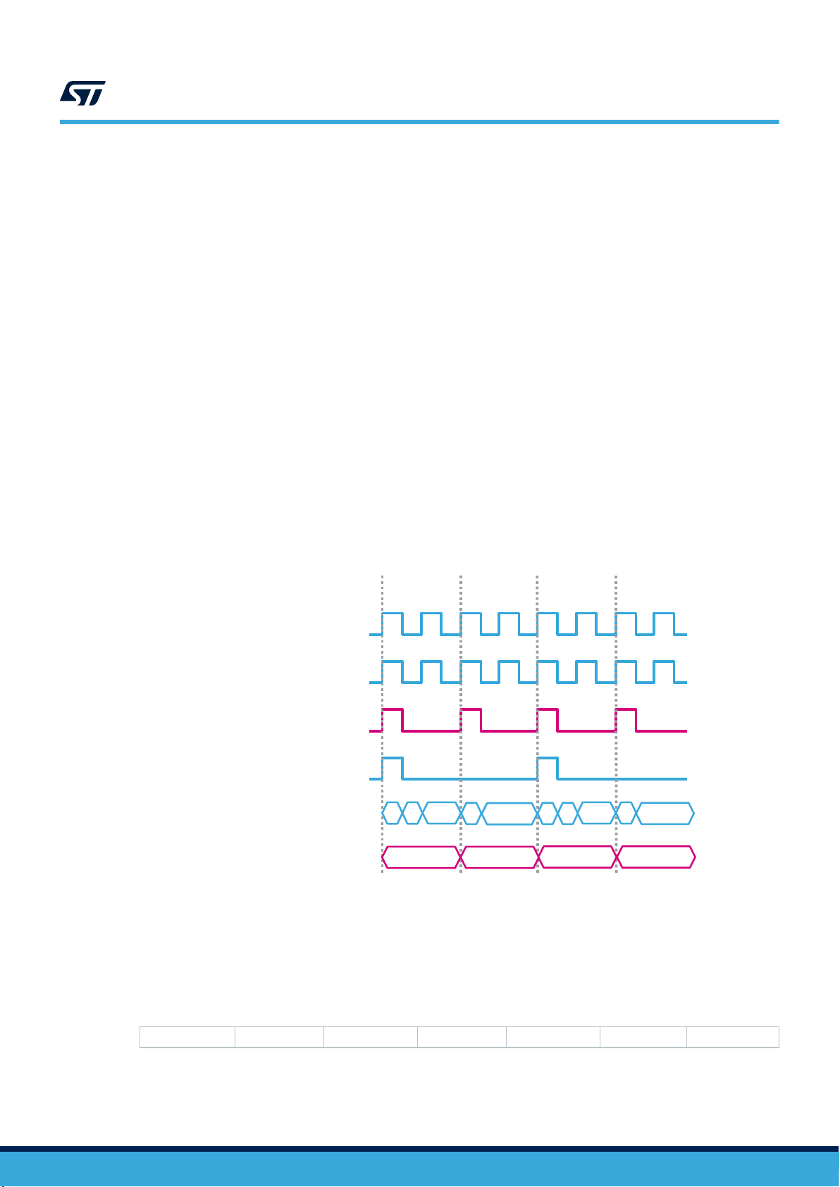
9.3 FIFO batched sensors
ODR_GY = 208 Hz DRDY
ODR_XL = 208 Hz DRDY
BDR_GY = 104 Hz event
BDR_XL = 52 Hz event
Time Slot (i)
Time Slot (i+1)
Time Slot (i+2)
Time Slot (i+3)
gyx
l
idle
idle
idle
idle
g
y
g
y
gyx
l
00 01
10 11
Write state
TAG counter
(synchronized with fastest BDR)
Time Slot frequency = max(BDR_GY, BDR_XL) = 104 Hz
As previously described, batched sensors can be classified in three different categories:
1. Main sensors;
2. Auxiliary sensors;
3. Virtual sensors.
In this section, all the details about each category will be presented.
AN5398
FIFO batched sensors
9.4
Main sensors
Main sensors are ISM330DHCX device physical sensors: accelerometer and gyroscope. The batch data rate can
be configured through the BDR_XL_[3:0] and BDR_GY_[3:0] fields of the FIFO_CTRL3 register. The batch data
rate must be equal to or lower than the relative sensor output data rate configured through the ODR_XL[3:0] and
ODR_G[3:0] field of the CTRL1_XL and CTRL2_G registers.
The main sensors define the FIFO time base. This means that each one of the other sensors can be associated
to a time base slot defined by the main sensors. A batch event of the fastest main sensor also increments the
TAG counter (TAG_CNT field of FIFO_DATA_OUT_TAG register). This counter is composed of two bits and its
value is continuously incremented (from 00b to 11b) to identify different time slots.
An example of a Batch Data Rate event is shown in Figure 27. Main sensors and time slot definitions. The
BDR_GY event and BDR_XL event identify the time in which the corresponding sensor data is written to the
FIFO. The evolution of the TAG counter identifies different time slots and its frequency is equivalent to the
maximum value between BDR_XL and BDR_GY.
Figure 27. Main sensors and time slot definitions
The FIFO word format of the main sensors is presented in the table below, representing the device addresses
from 78h to 7Eh.
AN5398 - Rev 3
Table 78. Main sensors output data format in FIFO
TAG
X_L X_H Y_L Y_H Z_L Z_H
page 90/132
Page 91

9.5 Auxiliary sensors
Auxiliary sensors are considered as service sensors for the main sensors. Auxiliary sensors include the:
• Temperature sensor (ODR_T_BATCH_[1:0] bits of the FIFO_CTRL4 register must be configured properly);
• Timestamp sensor: it stores the timestamp corresponding to a FIFO time slot (TIMESTAMP_EN bit of the
CTRL10_C register must be set to 1 and the DEC_TS_BATCH_[1:0] bits of the FIFO_CTRL4 register must
be configured properly);
• CFG-Change sensor: it identifies a change in some configuration of the device (ODRCHG_EN bit of the
FIFO_CTRL2 register must be set to 1).
Auxiliary sensors cannot trigger a write in FIFO. Their registers are written when the first main sensor or the
external sensor event occurs (even if they are configured at a higher batch data rate).
The temperature output data format in FIFO is presented in the following table.
TEMPERATURE[7:0] FIFO_DATA_OUT_X_L
TEMPERATURE[15:8] FIFO_DATA_OUT_X_H
AN5398
Auxiliary sensors
Table 79. Temperature output data format in FIFO
Data FIFO_DATA_OUT registers
0 FIFO_DATA_OUT_Y_L
0 FIFO_DATA_OUT_Y_H
0 FIFO_DATA_OUT_Z_L
0 FIFO_DATA_OUT_Z_H
The timestamp output data format in FIFO is presented in the following table.
Table 80. Timestamp output data format in FIFO
Data
TIMESTAMP[7:0] FIFO_DATA_OUT_X_L
TIMESTAMP[15:8] FIFO_DATA_OUT_X_H
TIMESTAMP[23:16] FIFO_DATA_OUT_Y_L
TIMESTAMP[31:24] FIFO_DATA_OUT_Y_H
BDR_SHUB FIFO_DATA_OUT_Z_L[3:0]
0 FIFO_DATA_OUT_Z_L[7:4]
BDR_XL FIFO_DATA_OUT_Z_H[3:0]
BDR_GY FIFO_DATA_OUT_Z_H[7:4]
FIFO_DATA_OUT registers
As shown in Table 80, timestamp data contain also some meta-information which can be used to detect a BDR
change if the CFG-Change sensor is not batched in FIFO: the batch data rate of both the main sensors and the
sensor hub. BDR_SHUB cannot be configured though a dedicated register. It is the result of the configured
sensor hub ODR through the SHUB_ODR_[1:0] bits of the SLAVE0_CONFIG sensor hub register and the
effective trigger sensor output data rate (the fastest between th accelerometer or gyroscope if the internal trigger
is used). For the complete description of BDR_SHUB, refer to to the next section about virtual sensors.
CFG-Change identifies a runtime change in the output data rate, the batch data rate or other configurations of the
main or virtual sensors. When a supported runtime change is applied, this sensor is written at the first new main
sensor or virtual sensor event followed by a timestamp sensor (also if the timestamp sensor is not batched).
This sensor can be used to correlate data from the sensors to the device timestamp without storing the timestamp
each time. It could be used also to notify the user to discard data due to embedded filters settling or to other
configuration changes (i.e switching mode, output data rate, …).
AN5398 - Rev 3
page 91/132
Page 92

CFG-Change output data format in FIFO is presented in the following table.
Table 81. CFG-change output data format in FIFO
Data FIFO_DATA_OUT registers
LPF1_SEL_G FIFO_DATA_OUT_X_H[0]
FTYPE[2:0] FIFO_DATA_OUT_X_H[3:1]
G_HM_MODE FIFO_DATA_OUT_X_H[4]
FS_125 FIFO_DATA_OUT_X_H[5]
FS[1:0]_G FIFO_DATA_OUT_X_H[7:6]
LPF2_XL_EN FIFO_DATA_OUT_Y_L[0]
HPCF_XL_[2:0] FIFO_DATA_OUT_Y_L[3:1]
XL_HM_MODE FIFO_DATA_OUT_Y_L[4]
0 FIFO_DATA_OUT_Y_L[5]
FS[1:0]_XL FIFO_DATA_OUT_Y_L[7:6]
BDR_SHUB FIFO_DATA_OUT_Y_H[3:0]
OIS enabled
Gyro startup
(1)
(2)
FIFO_COMPR_RT_EN FIFO_DATA_OUT_Y_H[7]
ODR_XL FIFO_DATA_OUT_Z_L[3:0]
ODR_GY FIFO_DATA_OUT_Z_L[7:4]
BDR_XL FIFO_DATA_OUT_Z_H[3:0]
BDR_GY FIFO_DATA_OUT_Z_H[7:4]
1. OIS enabled is asserted in two cases:
1. OIS_ON_EN = 1 and OIS_EN = 1 (OIS enabled from UI interface)
2. OIS_ON_EN = 0 and OIS_EN_SPI2 = 1 (OIS enabled from OIS interface)
2. Internal signal which is deasserted when gyroscope finishes startup phase (max startup time is 70 ms).
FIFO_DATA_OUT_Y_H[5]
FIFO_DATA_OUT_Y_H[6]
AN5398
Auxiliary sensors
AN5398 - Rev 3
page 92/132
Page 93

9.6 Virtual sensors
Virtual sensors are divided in two different categories:
1. External sensors, read from the sensor hub interface;
2. Step counter sensors.
9.6.1 External sensors and NACK sensor
Data of up to four external sensors read from the sensor hub (for a maximum of 18 bytes) can be stored in FIFO.
They are continuous virtual sensors with the batch data rate (BDR_SHUB) corresponding to the current value
of the SHUB_ODR_[1:0] field in the SLAVE0_CONFIG register, if an internal trigger is used (sensor hub read
triggered by the accelerometer or gyroscope data-ready signal). This value is limited by the effective trigger
sensor output data rate (the fastest between the accelerometer or gyroscope). If external sensors are not batched
or an external trigger is used, BDR_SHUB is set to 0.
The following table shows the possible values of the BDR_SHUB field.
BDR_SHUB BDR [Hz]
0000 Not batched or external trigger used
0001 12.5
0010 26
0011 52
0100 104
AN5398
Virtual sensors
Table 82. BDR_SHUB
As main sensors, external sensors define the FIFO time base and they can trigger the writing of auxiliary sensors
in FIFO (only if they are batched and an external trigger is not used).
It is possible to enable selectively the batching of the different external sensors using the
BATCH_EXT_SENS_0_EN, BATCH_EXT_SENS_1_EN, BATCH_EXT_SENS_2_EN, BATCH_EXT_SENS_3_EN
bits of the SLAVE0_CONFIG, SLAVE1_CONFIG, SLAVE2_CONFIG, SLAVE3_CONFIG sensor hub registers.
Each external sensor has a dedicated TAG value and 6 bytes reserved for data. External sensors are written
in FIFO in the same order of the sensor hub output registers and if the number of bytes read from an external
sensor is less than 6 bytes, then free bytes are filled with zeros.
If the communication with one external sensor batched in FIFO fails, the sensor hub writes a NACK sensor
instead of the corresponding sensor data in FIFO. A NACK sensor contains the index (numbered from 0 to 3) of
the failing slave and has the following output data format.
Table 83. Nack sensor output data format in FIFO
Data
Failing slave index FIFO_DATA_OUT_X_L[1:0]
0 FIFO_DATA_OUT_X_L[7:2]
0 FIFO_DATA_OUT_X_H
0 FIFO_DATA_OUT_Y_L
0 FIFO_DATA_OUT_Y_H
0 FIFO_DATA_OUT_Z_L
0 FIFO_DATA_OUT_Z_H
FIFO_DATA_OUT registers
AN5398 - Rev 3
page 93/132
Page 94

9.6.2 Step counter sensor
Step counter data, with associated timestamp, can be stored in FIFO. It is not a continuous rate sensor: the step
detection event triggers its writing in FIFO.
In order to enable the step counter sensor in FIFO, the user should:
1. Enable the step counter sensor (set the PEDO_EN bit to 1 in the EMB_FUNC_EN_A embedded functions
register);
2. Enable step counter batching (set the PEDO_FIFO_EN bit to 1 in the EMB_FUNC_FIFO_CFG embedded
functions register).
The format of the step counter data read from FIFO is shown in the table below.
STEP_COUNTER[7:0] FIFO_DATA_OUT_X_L
STEP_COUNTER[15:8] FIFO_DATA_OUT_X_H
TIMESTAMP[7:0] FIFO_DATA_OUT_Y_L
TIMESTAMP[15:8] FIFO_DATA_OUT_Y_H
TIMESTAMP[23:16] FIFO_DATA_OUT_Z_L
TIMESTAMP[31:24] FIFO_DATA_OUT_Z_H
AN5398
FIFO modes
Table 84. Step counter output data format in FIFO
Data FIFO_DATA_OUT registers
9.7 FIFO modes
The ISM330DHCX FIFO buffer can be configured to operate in six different modes, selectable through the
FIFO_MODE_[2:0] field of the FIFO_CTRL4 register. The available configurations ensure a high level of flexibility
and extend the number of functions usable in application development.
Bypass, FIFO, Continuous, Continuous-to-FIFO, Bypass-to-Continuous, and Bypass-to-FIFO modes are
described in the following paragraphs.
9.7.1 Bypass mode
When Bypass mode is enabled, the FIFO is not used, the buffer content is cleared, and it remains empty until
another mode is selected. Bypass mode is selected when the FIFO_MODE_[2:0] bits are set to 000b. Bypass
mode must be used in order to stop and reset the FIFO buffer when a different mode is intended to be used. Note
that by placing the FIFO buffer into Bypass mode, the whole buffer content is cleared.
AN5398 - Rev 3
page 94/132
Page 95

9.7.2 FIFO mode
511
F511
t
FIFO mode
enabled
FIFO
stops
FIFO_FULL_IA
FIFO mode
enabled
FIFO Reading
FIFO
Bypass
…
523522
…
510
……
543210
…
F1F0
…
F510
……
F5F4F3F2F1F0
FIFO word
Start FIFO
Reading
In FIFO mode, the buffer continues filling until it becomes full. Then it stops collecting data and the FIFO content
remains unchanged until a different mode is selected.
Follow these steps for FIFO mode configuration:
1. Enable the sensor data to be stored in FIFO with the corresponding batch data rate (if configurable);
2. Set the FIFO_MODE_[2:0] bits in the FIFO_CTRL4 register to 001b to enable FIFO mode.
When this mode is selected, the FIFO starts collecting data. The FIFO_STATUS1 and FIFO_STATUS2 registers
are updated according to the number of samples stored.
When the FIFO is full, the DIFF_FIFO_9 bit of the FIFO_STATUS2 register is set to 1 and no more data are
stored in the FIFO buffer. Data can be retrieved by reading all the FIFO_DATA_OUT (from 78h to 7Eh) registers
for the number of times specified by the DIFF_FIFO_[9:0] bits of the FIFO_STATUS1 and FIFO_STATUS2
registers.
Using the FIFO_WTM_IA bit of the FIFO_STATUS2 register, data can also be retrieved when a threshold level
(WTM[8:0] in FIFO_CTRL1 and FIFO_CTRL2 registers) is reached if the application requires a lower number of
samples in the FIFO.
If the STOP_ON_WTM bit of the FIFO_CTRL2 register is set to 1, the FIFO size is limited to the value of
the WTM[8:0] bits in the FIFO_CTRL1 and FIFO_CTRL2 registers. In this case, the FIFO_FULL_IA bit of the
FIFO_STATUS2 register is set high when the number of samples in FIFO will reach or exceed the WTM[8:0] value
on the next FIFO write operation.
Communication speed is not very important in FIFO mode because the data collection is stopped and there is no
risk of overwriting data already acquired. Before restarting the FIFO mode, it is necessary to set to Bypass mode
first in order to completely clear the FIFO content.
Figure 28. FIFO mode (STOP_ON_WTM = 0) shows an example of FIFO mode usage; the data from just one
sensor are stored in the FIFO. In these conditions, the number of samples that can be stored in the FIFO buffer
is 512 (with compression algorithm disabled). The FIFO_FULL_IA bit of the FIFO_STATUS2 register goes high
just after the level labeled as 510 to notify that the FIFO buffer will be completely filled at the next FIFO write
operation. After the FIFO is full (FIFO_DIFF_9 = 1), the data collection stops.
AN5398
FIFO modes
Figure 28. FIFO mode (STOP_ON_WTM = 0)
AN5398 - Rev 3
page 95/132
Page 96

9.7.3 Continuous mode
…
…
1022
……
F510
…
…
512
511
F1
F0
t
Continuous mode
enabled
FIFO_FULL_IA
FIFO Reading
Start FIFO
Reading
…
1024
1023
510
……
543210
…
F1F0F510
……
F5F4F3F2F1F0
FIFO word
Start FIFO
Reading
In Continuous mode, the FIFO continues filling. When the buffer is full, the FIFO index restarts from the beginning,
and older data are replaced by the new data. The oldest values continue to be overwritten until a read operation
frees FIFO slots. The host processor reading speed is important in order to free slots faster than new data is
made available. To stop this configuration, Bypass mode must be selected.
Follow these steps for Continuous mode configuration (if the accelerometer/gyroscope data-ready is used as the
FIFO trigger):
1. Enable the sensor data to be stored in FIFO with the corresponding batch data rate (if configurable);
2. Set the FIFO_MODE_[2:0] bits in the FIFO_CTRL4 register to 110b to enable FIFO mode.
When this mode is selected, the FIFO collects data continuously. The FIFO_STATUS1 and FIFO_STATUS2
registers are updated according to the number of samples stored. When the next FIFO write operation will make
the FIFO completely full or generate a FIFO overrun, the FIFO_FULL_IA bit of the FIFO_STATUS2 register goes
to 1. The FIFO_OVR_ IA and FIFO_OVR_LATCHED bits in the FIFO_STATUS2 register indicates when at least
one FIFO word has been overwritten to store the new data. Data can be retrieved after the FIFO_FULL_IA
event by reading the FIFO_DATA_OUT (from 78h to 7Eh) registers for the number of times specified by the
DIFF_FIFO_[9:0] bits in the FIFO_STATUS1 and FIFO_STATUS2 registers. Using the FIFO_WTM_IA bit of the
FIFO_STATUS2 register, data can also be retrieved when a threshold level (WTM[8:0] in the FIFO_CTRL1 and
FIFO_CTRL2 registers) is reached. If the STOP_ON_WTM bit of the FIFO_CTRL2 register is set to 1, the FIFO
size is limited to the value of the WTM[8:0] bits in the FIFO_CTRL1 and FIFO_CTRL2 registers. In this case, the
FIFO_FULL_IA bit of the FIFO_STATUS2 register goes high when the number of samples in FIFO will reach or
overcome the WTM[8:0] value on the next FIFO write operation.
Figure 29. Continuous mode shows an example of the Continuous mode usage. In the example, data from just
one sensor are stored in the FIFO and the FIFO samples are read on the FIFO_FULL_IA event and faster than 1
* ODR so that no data is lost. In these conditions, the number of samples stored is 511.
AN5398
FIFO modes
Figure 29. Continuous mode
AN5398 - Rev 3
page 96/132
Page 97

9.7.4 Continuous-to-FIFO mode
512
F509
513
F510
t
Continuous-to-FIFO
mode enabled
FIFO switches
to FIFO mode
FIFO_FULL_IA
FIFO Reading
FIFO
stops
514
…
…
543210
F511
…
…
F2F1F0
FIFO word
Start FIFO
Reading
Interrupt event
This mode is a combination of the Continuous and FIFO modes previously described. In Continuous-to-FIFO
mode, the FIFO buffer starts operating in Continuous mode and switches to FIFO mode when an event condition
occurs.
The event condition can be one of the following:
• Single tap: event detection has to be configured and the INT2_SINGLE_TAP bit of the MD2_CFG register
has to be set to 1;
• Double tap: event detection has to be configured and the INT2_DOUBLE_TAP bit of the MD2_CFG register
has to be set to 1;
• Free-fall: event detection has to be configured and the INT2_FF bit of the MD2_CFG register has to be set
to 1;
• Wake-up: event detection has to be configured and the INT2_WU bit of the MD2_CFG register has to be set
to 1;
• 6D: event detection has to be configured and the INT2_6D bit of the MD2_CFG register has to be set to 1.
Continuous-to-FIFO mode is sensitive to the edge of the interrupt signal. At the first interrupt event, FIFO changes
from Continuous mode to FIFO mode and maintains it until Bypass mode is set.
AN5398
FIFO modes
Figure 30. Continuous-to-FIFO mode
Follow these steps for Continuous-to-FIFO mode configuration (if the accelerometer/gyroscope data-ready is
used as the FIFO trigger):
1. Configure one of the events as previously described;
2. Enable the sensor data to be stored in FIFO with the corresponding batch data rate (if configurable);
AN5398 - Rev 3
3. Set the FIFO_MODE_[2:0] bits in the FIFO_CTRL4 register to 011b to enable FIFO Continuous-to-FIFO
mode.
In Continuous-to-FIFO mode the FIFO buffer continues filling. When the FIFO will be full or overrun at the next
FIFO write operation, the FIFO_FULL_IA bit goes high.
If the STOP_ON_WTM bit of the FIFO_CTRL2 register is set to 1, the FIFO size is limited to the value of
the WTM[8:0] bits in the FIFO_CTRL1 and FIFO_CTRL2 registers. In this case, the FIFO_FULL_IA bit of the
FIFO_STATUS2 register goes high when the number of samples in FIFO will reach or exceed the WTM[8:0] value
on the next FIFO write operation.
When the trigger event occurs, two different cases can be observed:
1. If the FIFO buffer is already full, it stops collecting data at the first sample after the event trigger. The FIFO
content is composed of the samples collected before the event.
2. If FIFO buffer is not full yet, it continues filling until it becomes full and then it stops collecting data.
page 97/132
Page 98
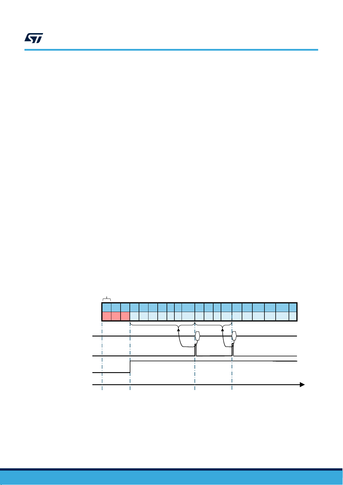
Continuous-to-FIFO can be used in order to analyze the history of the samples which have generated an
…
…
1028
1027
1026
…
…
F2F1
F0
1025
F510
…
…
513
F510
514
F0
t
Bypass-to-Continuous
mode enabled
FIFO switches to
Continuous mode
FIFO_FULL_IA
FIFO Reading
515
……
543210
F1
……
F2F1F0
FIFO word
Start FIFO
Reading
Interrupt event
Start FIFO
Reading
interrupt. The standard operation is to read the FIFO content when the FIFO mode is triggered and the FIFO
buffer is full and stopped.
9.7.5 Bypass-to-Continuous mode
This mode is a combination of the Bypass and Continuous modes previously described. In Bypass-to-Continuous
mode, the FIFO buffer starts operating in Bypass mode and switches to Continuous mode when an event
condition occurs.
The event condition can be one of the following:
• Single tap: event detection has to be configured and the INT2_SINGLE_TAP bit of the MD2_CFG register
has to be set to 1;
• Double tap: event detection has to be configured and the INT2_DOUBLE_TAP bit of the MD2_CFG register
has to be set to 1;
• Free-fall: event detection has to be configured and the INT2_FF bit of the MD2_CFG register has to be set
to 1;
• Wake-up: event detection has to be configured and the INT2_WU bit of the MD2_CFG register has to be set
to 1;
• 6D: event detection has to be configured and the INT2_6D bit of the MD2_CFG register has to be set to 1.
Bypass-to-Continuous mode is sensitive to the edge of the interrupt signal: at the first interrupt event, FIFO
changes from Bypass mode to Continuous mode and maintains it until Bypass mode is set.
Follow these steps for Bypass-to-Continuous mode configuration (if the accelerometer / gyroscope data-ready is
used as the FIFO trigger):
1. Configure one of the events as previously described;
2. Enable the sensor data to be stored in FIFO with the corresponding batch data rate (if configurable);
3. Set the FIFO_MODE[2:0] bits in the FIFO_CTRL4 register to 100b to enable FIFO Bypass-to-Continuous
mode.
Once the trigger condition appears and the buffer switches to Continuous mode, the FIFO buffer continues filling.
When the next stored set of data will make the FIFO full or overrun, the FIFO_FULL_IA bit is set high.
Bypass-to-Continuous can be used in order to start the acquisition when the configured interrupt is generated.
AN5398
FIFO modes
Figure 31. Bypass-to-Continuous mode
AN5398 - Rev 3
page 98/132
Page 99

9.7.6 Bypass-to-FIFO mode
513
F510
514
F511
t
Bypass-to-FIFO
mode enabled
FIFO switches to
FIFO mode
FIFO_FULL_IA
FIFO Reading
……
543210
……
F2F1F0
FIFO word
FIFO
stops
Interrupt event
Start FIFO
Reading
This mode is a combination of the Bypass and FIFO modes previously described. In Bypass-to-FIFO mode, the
FIFO buffer starts operating in Bypass mode and switches to FIFO mode when an event condition occurs.
The event condition can be one of the following:
• Single tap: event detection has to be configured and the INT2_SINGLE_TAP bit of the MD2_CFG register
has to be set to 1;
• Double tap: event detection has to be configured and the INT2_DOUBLE_TAP bit of the MD2_CFG register
has to be set to 1;
• Free-fall: event detection has to be configured and the INT2_FF bit of the MD2_CFG register has to be set
to 1;
• Wake-up: event detection has to be configured and the INT2_WU bit of the MD2_CFG register has to be set
to 1;
• 6D: event detection has to be configured and the INT2_6D bit of the MD2_CFG register has to be set to 1.
Bypass-to-FIFO mode is sensitive to the edge of the interrupt signal. At the first interrupt event, FIFO changes
from Bypass mode to FIFO mode and maintains it until Bypass mode is set.
Follow these steps for Bypass-to-FIFO mode configuration (if the accelerometer / gyroscope data-ready is used
as the FIFO trigger):
1. Configure one of the events as previously described;
2. Enable the sensor data to be stored in FIFO with the corresponding batch data rate (if configurable);
3. Set the FIFO_MODE_[2:0] bits in the FIFO_CTRL4 register to 111b to enable FIFO Bypass-to-FIFO mode.
Once the trigger condition appears and the buffer switches to FIFO mode, the FIFO buffer starts filling. When the
next stored set of data will make the FIFO full or overrun, the FIFO_FULL_IA bit is set high and the FIFO stops.
Bypass-to-FIFO can be used in order to analyze the history of the samples which have generated an interrupt.
AN5398
FIFO modes
Figure 32. Bypass-to-FIFO mode
AN5398 - Rev 3
page 99/132
Page 100

9.8 Retrieving data from the FIFO
When FIFO is enabled and the mode is different from Bypass, reading the FIFO output registers return the oldest
FIFO sample set. Whenever these registers are read, their content is moved to the SPI/I²C output buffer.
FIFO slots are ideally shifted up one level in order to release room for a new sample, and the FIFO output
registers load the current oldest value stored in the FIFO buffer.
The recommended way to retrieve data from the FIFO is the following:
1. Read the FIFO_STATUS1 and FIFO_STATUS2 registers to check how many words are stored in the FIFO.
This information is contained in the DIFF_FIFO_[9:0] bits.
2. For each word in FIFO, read the FIFO word (tag and output data) and interpret it on the basis of the FIFO
tag.
3. Go to step 1.
The entire FIFO content is retrieved by performing a certain number of read operations from the FIFO output
registers until the buffer becomes empty (DIFF_FIFO_[9:0] bits of the FIFO_STATUS1 and FIFO_STATUS2
register are equal to 0).
It is recommended to avoid reading from FIFO when it is empty.
FIFO output data must be read with multiple of 7 bytes reads starting from the FIFO_DATA_OUT_TAG register.
The rounding function from address FIFO_DATA_OUT_Z_H to FIFO_DATA_OUT_TAG is done automatically in
the device, in order to allow reading many words with a unique multiple read operation.
AN5398
Retrieving data from the FIFO
AN5398 - Rev 3
page 100/132
 Loading...