

Page 1
UM2403
User manual
Evaluation board with STM32G081RB MCU
Introduction
The STM32G081B-EVAL Evaluation board is a high-end development platform for Arm®
®
Cortex
Delivery controller interfaces (UCPD) compliant with USB Type-C r1.2 and USB PD
specification r3.0, two I2Cs, two SPIs, five USARTs, one LP UART, one 12-bit ADC, two
12-bit DACs, two GP comparators, two LP timers, internal 32KB SRAM and 128KB Flash,
CEC, SWD debugging support.
The full range of hardware features on the STM32G081B-EVAL Evaluation board includes
the mother board, the legacy peripheral daughterboard and the USB Type-C and Power
Delivery daughterboard, which help to evaluate all peripherals (USB Type-C connector with
USB PD, motor control connector, RS232, RS485, Audio DAC, microphone ADC, TFT LCD,
IrDA, IR LED, IR receiver, LDR, microSD
slot, RF E2PROM and temperature sensor… etc.) and to develop applications. An STLINK/V2-1 is integrated on the board as embedded in-circuit debugger and programmer for
the STM32 MCU
-M0+ core-based STM32G081RBT6 microcontroller with USB Type-C™ and Power
™
card, CEC on two HDMI connectors, smartcard
.
The daughterboard and extension connectors provide an easy way to connect a
daughterboard or wrapping board for your specific application.
The USB Type-C and Power Delivery daughterboard features two independent USB-C ports
controlled by STM32G0. USB-C port 1 is dual role power (DRP) and can provide up-to 45W
of power. USB-C Port 2 is sink only. Both supports USB PD protocol and alternate mode
functionality.
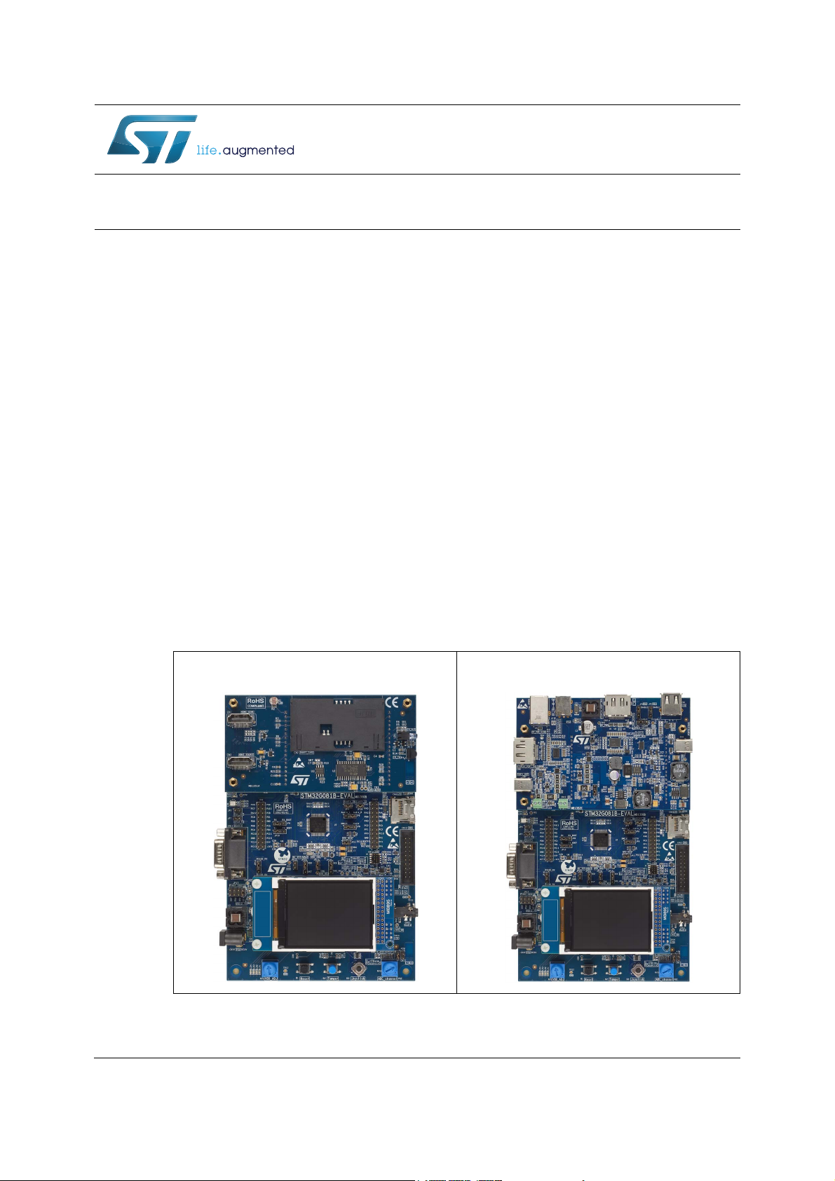
Figure 1. STM32G081B-EVAL board with
legacy peripheral daughterboard
Figure 2. STM32G081B-EVAL board with
UCPD daughterboard
Pictures are not contractual.
November 2018 UM2403 Rev 1 1/78
www.st.com
1
Page 2

Contents UM2403
Contents
1 Features . . . . . . . . . . . . . . . . . . . . . . . . . . . . . . . . . . . . . . . . . . . . . . . . . . . 8
2 Product marking . . . . . . . . . . . . . . . . . . . . . . . . . . . . . . . . . . . . . . . . . . . 10
3 System requirements . . . . . . . . . . . . . . . . . . . . . . . . . . . . . . . . . . . . . . . 10
4 Development toolchains . . . . . . . . . . . . . . . . . . . . . . . . . . . . . . . . . . . . . 10
5 Demonstration software . . . . . . . . . . . . . . . . . . . . . . . . . . . . . . . . . . . . . 10
6 Ordering information . . . . . . . . . . . . . . . . . . . . . . . . . . . . . . . . . . . . . . . 11
7 Delivery recommendations . . . . . . . . . . . . . . . . . . . . . . . . . . . . . . . . . . 11
8 Hardware layout and configuration . . . . . . . . . . . . . . . . . . . . . . . . . . . . 12
8.1 Embedded ST-LINK/V2-1 . . . . . . . . . . . . . . . . . . . . . . . . . . . . . . . . . . . . . 15
8.1.1 Drivers . . . . . . . . . . . . . . . . . . . . . . . . . . . . . . . . . . . . . . . . . . . . . . . . . . 15
8.1.2 ST-LINK/V2-1 firmware upgrade . . . . . . . . . . . . . . . . . . . . . . . . . . . . . . 15
8.2 Power supply . . . . . . . . . . . . . . . . . . . . . . . . . . . . . . . . . . . . . . . . . . . . . . 16
8.3 Clock references . . . . . . . . . . . . . . . . . . . . . . . . . . . . . . . . . . . . . . . . . . . 20
8.4 Reset source . . . . . . . . . . . . . . . . . . . . . . . . . . . . . . . . . . . . . . . . . . . . . . 20
8.5 Boot Option . . . . . . . . . . . . . . . . . . . . . . . . . . . . . . . . . . . . . . . . . . . . . . . 21
8.6 Peripherals on mother board . . . . . . . . . . . . . . . . . . . . . . . . . . . . . . . . . . 21
8.6.1 Audio . . . . . . . . . . . . . . . . . . . . . . . . . . . . . . . . . . . . . . . . . . . . . . . . . . . 21
8.6.2 RS232 and RS485 . . . . . . . . . . . . . . . . . . . . . . . . . . . . . . . . . . . . . . . . . 22
8.6.3 microSD card . . . . . . . . . . . . . . . . . . . . . . . . . . . . . . . . . . . . . . . . . . . . . 23
8.6.4 Analog Input . . . . . . . . . . . . . . . . . . . . . . . . . . . . . . . . . . . . . . . . . . . . . . 23
8.6.5 External I2C Connector . . . . . . . . . . . . . . . . . . . . . . . . . . . . . . . . . . . . . 23
8.6.6 Motor Control . . . . . . . . . . . . . . . . . . . . . . . . . . . . . . . . . . . . . . . . . . . . . 24
8.6.7 Display and Input devices . . . . . . . . . . . . . . . . . . . . . . . . . . . . . . . . . . . 24
8.7 Peripherals on legacy peripheral daughterboard . . . . . . . . . . . . . . . . . . . 25
8.7.1 LDR (Light dependent resistor) . . . . . . . . . . . . . . . . . . . . . . . . . . . . . . . 25
8.7.2 Temperature sensor . . . . . . . . . . . . . . . . . . . . . . . . . . . . . . . . . . . . . . . . 25
8.7.3 Smartcard . . . . . . . . . . . . . . . . . . . . . . . . . . . . . . . . . . . . . . . . . . . . . . . 26
2/78 UM2403 Rev 1
Page 3

UM2403 Contents
8.7.4 HDMI CEC . . . . . . . . . . . . . . . . . . . . . . . . . . . . . . . . . . . . . . . . . . . . . . . 26
8.7.5 IR LED and IR receiver . . . . . . . . . . . . . . . . . . . . . . . . . . . . . . . . . . . . . 27
8.8 USB Type-C and Power Delivery daughterboard . . . . . . . . . . . . . . . . . . . 27
8.8.1 USB Type-C receptacles . . . . . . . . . . . . . . . . . . . . . . . . . . . . . . . . . . . . 27
8.8.2 Power Delivery and local power management . . . . . . . . . . . . . . . . . . . 28
8.8.3 VBUS management and discharge mechanism . . . . . . . . . . . . . . . . . . 28
8.8.4 VBUS voltage-sensing and current-sense stage . . . . . . . . . . . . . . . . . . 29
8.8.5 CC management . . . . . . . . . . . . . . . . . . . . . . . . . . . . . . . . . . . . . . . . . . 29
9 Connectors . . . . . . . . . . . . . . . . . . . . . . . . . . . . . . . . . . . . . . . . . . . . . . . 31
9.1 Connectors on mother board . . . . . . . . . . . . . . . . . . . . . . . . . . . . . . . . . . 31
9.1.1 Motor control connector CN1 . . . . . . . . . . . . . . . . . . . . . . . . . . . . . . . . . 31
9.1.2 External I2C connector CN2 . . . . . . . . . . . . . . . . . . . . . . . . . . . . . . . . . 32
9.1.3 Daughterboard connector CN4 and CN5 . . . . . . . . . . . . . . . . . . . . . . . . 32
9.1.4 ST-LINK/V2-1 USB Micro-B connector CN6 . . . . . . . . . . . . . . . . . . . . . 34
9.1.5 ST-LINK/V2-1 programming connector CN7 . . . . . . . . . . . . . . . . . . . . . 35
9.1.6 microSD connector CN8 . . . . . . . . . . . . . . . . . . . . . . . . . . . . . . . . . . . . 35
9.1.7 Extension connector CN9 and CN10 . . . . . . . . . . . . . . . . . . . . . . . . . . . 35
9.1.8 RS232 and RS485 connector CN11 . . . . . . . . . . . . . . . . . . . . . . . . . . . 37
9.1.9 Standard SWD connector CN12 . . . . . . . . . . . . . . . . . . . . . . . . . . . . . . 38
9.1.10 High density SWD connector CN13 . . . . . . . . . . . . . . . . . . . . . . . . . . . . 39
9.1.11 TFT LCD connector CN14 . . . . . . . . . . . . . . . . . . . . . . . . . . . . . . . . . . . 39
9.1.12 Audio jack CN15 . . . . . . . . . . . . . . . . . . . . . . . . . . . . . . . . . . . . . . . . . . 39
9.1.13 5 V Power connector CN16 . . . . . . . . . . . . . . . . . . . . . . . . . . . . . . . . . . 39
9.1.14 Analog input connector CN17 . . . . . . . . . . . . . . . . . . . . . . . . . . . . . . . . 40
9.2 Connectors on legacy peripheral daughterboard . . . . . . . . . . . . . . . . . . . 40
9.2.1 HDMI sink connector CN1 . . . . . . . . . . . . . . . . . . . . . . . . . . . . . . . . . . . 40
9.2.2 Smartcard connector CN2 . . . . . . . . . . . . . . . . . . . . . . . . . . . . . . . . . . . 41
9.2.3 HDMI source connector CN3 . . . . . . . . . . . . . . . . . . . . . . . . . . . . . . . . . 42
9.2.4 Daughterboard female connector CN4 and CN5 . . . . . . . . . . . . . . . . . . 42
9.3 Connectors on UCPD daughterboard . . . . . . . . . . . . . . . . . . . . . . . . . . . 42
9.3.1 USB Type A connector CN1 . . . . . . . . . . . . . . . . . . . . . . . . . . . . . . . . . 42
9.3.2 DisplayPort source connector CN2 . . . . . . . . . . . . . . . . . . . . . . . . . . . . 43
9.3.3 19 V Power connector CN3 . . . . . . . . . . . . . . . . . . . . . . . . . . . . . . . . . . 43
9.3.4 USB3.1 Gen1 Type B connector CN4 . . . . . . . . . . . . . . . . . . . . . . . . . . 44
9.3.5 USB Type-C connector PORT2 CN5 . . . . . . . . . . . . . . . . . . . . . . . . . . . 44
9.3.6 Display port sink connector CN6 . . . . . . . . . . . . . . . . . . . . . . . . . . . . . . 45
UM2403 Rev 1 3/78
4
Page 4

Contents UM2403
9.3.7 USB Type-C connector PORT1 CN7 . . . . . . . . . . . . . . . . . . . . . . . . . . . 46
9.3.8 Daughterboard female connector CN8 and CN9 . . . . . . . . . . . . . . . . . . 46
Appendix A Electrical schematics . . . . . . . . . . . . . . . . . . . . . . . . . . . . . . . . . . . . 47
Appendix B STM32G081B-EVAL IO Assignment . . . . . . . . . . . . . . . . . . . . . . . . . 72
Appendix C Federal Communications Commission (FCC) and
Industry Canada (IC) Compliance Statements . . . . . . . . . . . . . . . . 75
C.1 FCC Compliance Statement . . . . . . . . . . . . . . . . . . . . . . . . . . . . . . . . . . . 75
C.1.1 Part 15.19 . . . . . . . . . . . . . . . . . . . . . . . . . . . . . . . . . . . . . . . . . . . . . . . . 75
C.1.2 Part 15.105 . . . . . . . . . . . . . . . . . . . . . . . . . . . . . . . . . . . . . . . . . . . . . . . 75
C.1.3 Part 15.21 . . . . . . . . . . . . . . . . . . . . . . . . . . . . . . . . . . . . . . . . . . . . . . . . 75
C.2 IC Compliance Statement . . . . . . . . . . . . . . . . . . . . . . . . . . . . . . . . . . . . . 75
C.2.1 Compliance Statement . . . . . . . . . . . . . . . . . . . . . . . . . . . . . . . . . . . . . . 75
C.3 Déclaration de conformité . . . . . . . . . . . . . . . . . . . . . . . . . . . . . . . . . . . . . 75
Appendix D Mechanical dimensions. . . . . . . . . . . . . . . . . . . . . . . . . . . . . . . . . . . 76
Revision history . . . . . . . . . . . . . . . . . . . . . . . . . . . . . . . . . . . . . . . . . . . . . . . . . . . . 77
4/78 UM2403 Rev 1
Page 5

UM2403 List of tables
List of tables
Table 1. Ordering information . . . . . . . . . . . . . . . . . . . . . . . . . . . . . . . . . . . . . . . . . . . . . . . . . . . . . . 11
Table 2. Power source related Jumpers . . . . . . . . . . . . . . . . . . . . . . . . . . . . . . . . . . . . . . . . . . . . . . 18
Table 3. Low voltage limitation . . . . . . . . . . . . . . . . . . . . . . . . . . . . . . . . . . . . . . . . . . . . . . . . . . . . . 19
Table 4. 32 KHz crystal X2 related solder bridges . . . . . . . . . . . . . . . . . . . . . . . . . . . . . . . . . . . . . . 20
Table 5. 8 MHz crystal X3 related solder bridges . . . . . . . . . . . . . . . . . . . . . . . . . . . . . . . . . . . . . . . 20
Table 6. Boot related jumper . . . . . . . . . . . . . . . . . . . . . . . . . . . . . . . . . . . . . . . . . . . . . . . . . . . . . . 21
Table 7. Boot0 related jumpers. . . . . . . . . . . . . . . . . . . . . . . . . . . . . . . . . . . . . . . . . . . . . . . . . . . . . 21
Table 8. Audio related jumpers . . . . . . . . . . . . . . . . . . . . . . . . . . . . . . . . . . . . . . . . . . . . . . . . . . . . . 22
Table 9. RS232 and RS485 related jumpers . . . . . . . . . . . . . . . . . . . . . . . . . . . . . . . . . . . . . . . . . . 22
Table 10. RS485 related solder bridges . . . . . . . . . . . . . . . . . . . . . . . . . . . . . . . . . . . . . . . . . . . . . . . 23
Table 11. LCD modules . . . . . . . . . . . . . . . . . . . . . . . . . . . . . . . . . . . . . . . . . . . . . . . . . . . . . . . . . . . 24
Table 12. Temperature sensor related solder bridge . . . . . . . . . . . . . . . . . . . . . . . . . . . . . . . . . . . . . 25
Table 13. Connection between ST8024L and STM32G081RBT6 . . . . . . . . . . . . . . . . . . . . . . . . . . . 26
Table 14. VBUS related jumpers . . . . . . . . . . . . . . . . . . . . . . . . . . . . . . . . . . . . . . . . . . . . . . . . . . . . 28
Table 15. Local power related jumpers. . . . . . . . . . . . . . . . . . . . . . . . . . . . . . . . . . . . . . . . . . . . . . . . 28
Table 16. VBUS Power Delivery profiles . . . . . . . . . . . . . . . . . . . . . . . . . . . . . . . . . . . . . . . . . . . . . . 29
Table 17. Voltage-sensing and current-sensing ADC. . . . . . . . . . . . . . . . . . . . . . . . . . . . . . . . . . . . . 29
Table 18. Dead battery related jumpers . . . . . . . . . . . . . . . . . . . . . . . . . . . . . . . . . . . . . . . . . . . . . . . 30
Table 19. Motor control connector CN1 . . . . . . . . . . . . . . . . . . . . . . . . . . . . . . . . . . . . . . . . . . . . . . . 31
Table 20. RF E2PROM connector CN2 . . . . . . . . . . . . . . . . . . . . . . . . . . . . . . . . . . . . . . . . . . . . . . . 32
Table 21. Daughterboard connector CN4 . . . . . . . . . . . . . . . . . . . . . . . . . . . . . . . . . . . . . . . . . . . . . . 33
Table 22. Daughterboard connector CN5 . . . . . . . . . . . . . . . . . . . . . . . . . . . . . . . . . . . . . . . . . . . . . . 33
Table 23. USB Micro-B connector CN6 . . . . . . . . . . . . . . . . . . . . . . . . . . . . . . . . . . . . . . . . . . . . . . . 34
Table 24. microSD connector CN9 . . . . . . . . . . . . . . . . . . . . . . . . . . . . . . . . . . . . . . . . . . . . . . . . . . . 35
Table 25. Extension connector CN9 . . . . . . . . . . . . . . . . . . . . . . . . . . . . . . . . . . . . . . . . . . . . . . . . . . 36
Table 26. Extension connector CN10 . . . . . . . . . . . . . . . . . . . . . . . . . . . . . . . . . . . . . . . . . . . . . . . . . 36
Table 27. RS232 & RS485 connector CN11 . . . . . . . . . . . . . . . . . . . . . . . . . . . . . . . . . . . . . . . . . . . 37
Table 28. Standard SWD debugging connector CN12 . . . . . . . . . . . . . . . . . . . . . . . . . . . . . . . . . . . . 38
Table 29. High density SWD debugging connector CN13 . . . . . . . . . . . . . . . . . . . . . . . . . . . . . . . . . 39
Table 30. Analog input-output connector CN17 . . . . . . . . . . . . . . . . . . . . . . . . . . . . . . . . . . . . . . . . . 40
Table 31. HDMI sink connector CN1 . . . . . . . . . . . . . . . . . . . . . . . . . . . . . . . . . . . . . . . . . . . . . . . . . 40
Table 32. Smartcard connector CN2 . . . . . . . . . . . . . . . . . . . . . . . . . . . . . . . . . . . . . . . . . . . . . . . . . 41
Table 33. HDMI source connector CN3 . . . . . . . . . . . . . . . . . . . . . . . . . . . . . . . . . . . . . . . . . . . . . . . 42
Table 34. USB Type A connector CN1 . . . . . . . . . . . . . . . . . . . . . . . . . . . . . . . . . . . . . . . . . . . . . . . . 42
Table 35. DisplayPort source connector CN2. . . . . . . . . . . . . . . . . . . . . . . . . . . . . . . . . . . . . . . . . . . 43
Table 36. USB3.1 Gen1 Type B connector CN4 . . . . . . . . . . . . . . . . . . . . . . . . . . . . . . . . . . . . . . . . 44
Table 37. USB Type-C connector PORT2 CN5 . . . . . . . . . . . . . . . . . . . . . . . . . . . . . . . . . . . . . . . . . 44
Table 38. DisplayPort sink connector CN6 . . . . . . . . . . . . . . . . . . . . . . . . . . . . . . . . . . . . . . . . . . . . . 45
Table 39. USB Type-C connector PORT1 CN7 . . . . . . . . . . . . . . . . . . . . . . . . . . . . . . . . . . . . . . . . . 46
Table 40. STM32G081B-EVAL IO Assignment . . . . . . . . . . . . . . . . . . . . . . . . . . . . . . . . . . . . . . . . . 72
Table 41. Mechanical dimensions . . . . . . . . . . . . . . . . . . . . . . . . . . . . . . . . . . . . . . . . . . . . . . . . . . . 76
Table 42. Document revision history . . . . . . . . . . . . . . . . . . . . . . . . . . . . . . . . . . . . . . . . . . . . . . . . . 77
UM2403 Rev 1 5/78
5
Page 6

List of figures UM2403
List of figures
Figure 1. STM32G081B-EVAL board with legacy peripheral daughterboard . . . . . . . . . . . . . . . . . . . 1
Figure 2. STM32G081B-EVAL board with UCPD daughterboard . . . . . . . . . . . . . . . . . . . . . . . . . . . . 1
Figure 3. Hardware block diagram. . . . . . . . . . . . . . . . . . . . . . . . . . . . . . . . . . . . . . . . . . . . . . . . . . . 12
Figure 4. STM32G081B-EVAL Evaluation board layout . . . . . . . . . . . . . . . . . . . . . . . . . . . . . . . . . . 13
Figure 5. Legacy peripheral daughterboard. . . . . . . . . . . . . . . . . . . . . . . . . . . . . . . . . . . . . . . . . . . . 14
Figure 6. USB Type-C and Power Delivery daughterboard. . . . . . . . . . . . . . . . . . . . . . . . . . . . . . . . 14
Figure 7. USB Composite Device . . . . . . . . . . . . . . . . . . . . . . . . . . . . . . . . . . . . . . . . . . . . . . . . . . . 15
Figure 8. 5 V power structure. . . . . . . . . . . . . . . . . . . . . . . . . . . . . . . . . . . . . . . . . . . . . . . . . . . . . . . 17
Figure 9. GP comparator 1 . . . . . . . . . . . . . . . . . . . . . . . . . . . . . . . . . . . . . . . . . . . . . . . . . . . . . . . . 25
Figure 10. Motor Control connector CN1 (top view) . . . . . . . . . . . . . . . . . . . . . . . . . . . . . . . . . . . . . . 31
Figure 11. I2C EXT connector CN2 (front view) . . . . . . . . . . . . . . . . . . . . . . . . . . . . . . . . . . . . . . . . . 32
Figure 12. USB Micro-B connector CN6 (front view) . . . . . . . . . . . . . . . . . . . . . . . . . . . . . . . . . . . . . . 34
Figure 13. microSD connector CN8 (front view) . . . . . . . . . . . . . . . . . . . . . . . . . . . . . . . . . . . . . . . . . 35
Figure 14. RS232 and RS485 connector CN11 (front view) . . . . . . . . . . . . . . . . . . . . . . . . . . . . . . . . 37
Figure 15. Standard SWD debugging connector CN12 (top view) . . . . . . . . . . . . . . . . . . . . . . . . . . . 38
Figure 16. High density SWD debugging connector CN13 (top view) . . . . . . . . . . . . . . . . . . . . . . . . . 39
Figure 17. Power-supply connector CN16 (front view) . . . . . . . . . . . . . . . . . . . . . . . . . . . . . . . . . . . . 39
Figure 18. Analog input-output connector CN17 (top view). . . . . . . . . . . . . . . . . . . . . . . . . . . . . . . . . 40
Figure 19. HDMI sink connector CN1 (front view) . . . . . . . . . . . . . . . . . . . . . . . . . . . . . . . . . . . . . . . . 40
Figure 20. Smartcard connector CN2 (top view) . . . . . . . . . . . . . . . . . . . . . . . . . . . . . . . . . . . . . . . . . 41
Figure 21. HDMI source connector CN3 (front view) . . . . . . . . . . . . . . . . . . . . . . . . . . . . . . . . . . . . . . 42
Figure 22. USB Type A connector CN1 (front view) . . . . . . . . . . . . . . . . . . . . . . . . . . . . . . . . . . . . . . 42
Figure 23. DisplayPort source connector CN2 (front view) . . . . . . . . . . . . . . . . . . . . . . . . . . . . . . . . . 43
Figure 24. 19 V Power connector CN3 (front view) . . . . . . . . . . . . . . . . . . . . . . . . . . . . . . . . . . . . . . . 43
Figure 25. USB3.1 Gen1 Type B connector CN4 (front view) . . . . . . . . . . . . . . . . . . . . . . . . . . . . . . . 44
Figure 26. USB Type-C connector PORT2 CN5 (front view) . . . . . . . . . . . . . . . . . . . . . . . . . . . . . . . . 44
Figure 27. DisplayPort sink connector CN6 (front view) . . . . . . . . . . . . . . . . . . . . . . . . . . . . . . . . . . . 45
Figure 28. USB Type-C connector PORT1 CN7 (front view) . . . . . . . . . . . . . . . . . . . . . . . . . . . . . . . . 46
Figure 29. STM32G081B-EVAL mother board top . . . . . . . . . . . . . . . . . . . . . . . . . . . . . . . . . . . . . . . 48
Figure 30. STM32G081B-EVAL MCU . . . . . . . . . . . . . . . . . . . . . . . . . . . . . . . . . . . . . . . . . . . . . . . . . 49
Figure 31. STM32G081B-EVAL power . . . . . . . . . . . . . . . . . . . . . . . . . . . . . . . . . . . . . . . . . . . . . . . . 50
Figure 32. STM32G081B-EVAL audio . . . . . . . . . . . . . . . . . . . . . . . . . . . . . . . . . . . . . . . . . . . . . . . . . 51
Figure 33. STM32G081B-EVAL LCD microSD . . . . . . . . . . . . . . . . . . . . . . . . . . . . . . . . . . . . . . . . . . 52
Figure 34. STM32G081B-EVAL motor-control . . . . . . . . . . . . . . . . . . . . . . . . . . . . . . . . . . . . . . . . . . 53
Figure 35. STM32G081B-EVAL peripherals . . . . . . . . . . . . . . . . . . . . . . . . . . . . . . . . . . . . . . . . . . . . 54
Figure 36. STM32G081B-EVAL RS232 and RS485 . . . . . . . . . . . . . . . . . . . . . . . . . . . . . . . . . . . . . . 55
Figure 37. STM32G081B-EVAL extension connectors . . . . . . . . . . . . . . . . . . . . . . . . . . . . . . . . . . . . 56
Figure 38. STM32G081B-EVAL ST-LINK V2-1 . . . . . . . . . . . . . . . . . . . . . . . . . . . . . . . . . . . . . . . . . . 57
Figure 39. STM32G081B-EVAL SWD . . . . . . . . . . . . . . . . . . . . . . . . . . . . . . . . . . . . . . . . . . . . . . . . . 58
Figure 40. STM32G081B-EVAL legacy peripheral daughterboard . . . . . . . . . . . . . . . . . . . . . . . . . . . 59
Figure 41. STM32G081B-EVAL legacy peripheral daughterboard HDMI and CEC . . . . . . . . . . . . . . 60
Figure 42. STM32G081B-EVAL legacy peripheral daughterboard Smartcard and IR. . . . . . . . . . . . . 61
Figure 43. STM32G081B-EVAL legacy peripheral daughterboard temperature sensor and LDR. . . . 62
Figure 44. STM32G081B-EVAL UCPD daughterboard top . . . . . . . . . . . . . . . . . . . . . . . . . . . . . . . . . 63
Figure 45. STM32G081B-EVAL UCPD daughterboard CC and VCONN . . . . . . . . . . . . . . . . . . . . . . 64
Figure 46. STM32G081B-EVAL UCPD daughterboard port1 DP USB3 . . . . . . . . . . . . . . . . . . . . . . . 65
Figure 47. STM32G081B-EVAL UCPD daughterboard Type-C source con . . . . . . . . . . . . . . . . . . . . 66
Figure 48. STM32G081B-EVAL UCPD daughterboard port2 DP . . . . . . . . . . . . . . . . . . . . . . . . . . . . 67
6/78 UM2403 Rev 1
Page 7

UM2403 List of figures
Figure 49. STM32G081B-EVAL UCPD daughterboard Type-C sink con . . . . . . . . . . . . . . . . . . . . . . 68
Figure 50. STM32G081B-EVAL UCPD daughterboard USB PD. . . . . . . . . . . . . . . . . . . . . . . . . . . . . 69
Figure 51. STM32G081B-EVAL UCPD daughterboard power . . . . . . . . . . . . . . . . . . . . . . . . . . . . . . 70
Figure 52. STM32G081B-EVAL UCPD daughterboard source power. . . . . . . . . . . . . . . . . . . . . . . . . 71
Figure 53. Mechanical dimensions . . . . . . . . . . . . . . . . . . . . . . . . . . . . . . . . . . . . . . . . . . . . . . . . . . . 76
UM2403 Rev 1 7/78
7
Page 8
Features UM2403
1 Features
Mother board
• STM32G081RBT6 Arm
of Flash memory and 32 Kbytes of RAM in LQFP64 package
• MCU voltage choice fixed 3.3 V or adjustable from 1.65 V to 3.6 V
2
• I
C compatible serial interface
• RTC with backup battery
• 8-Gbyte or more SPI interface microSD
• Potentiometer
• 4 color user LEDs and one LED as MCU low-power alarm
• Reset, Tamper and User buttons
• 4-direction control and selection joystick
• Board connectors:
– 5 V power jack
– RS-232 and RS485 communications
– Stereo audio jack including analog microphone input
–microSD™ card
– Extension I
2
– Motor-control connector
• Board extension connectors:
– Daughterboard connectors for legacy peripheral daughterboard or USB Type-C
and Power Delivery daughterboard
– Extension connectors for daughterboard or wire-wrap board
• Flexible power-supply options:
– 5 V power jack
– ST-LINK/V2-1 USB connector
– Daughterboard
• On-board ST-LINK/V2-1 debugger/programmer with USB enumeration capability:
mass storage, virtual COM port and debug port
• Comprehensive free software libraries and examples available with the STM32Cube
package
• Support of a wide choice of Integrated Development Environments (IDEs) including
IAR™, Keil
®
, GCC-based IDEs.
®(a)
Cortex®-M0+ core-based microcontroller with 128 Kbytes
C connector
™
card
a. Arm is a registered trademark of Arm Limited (or its subsidiaries) in the US and/or elsewhere.
8/78 UM2403 Rev 1
Page 9

UM2403 Features
Legacy peripheral daughterboard
• IrDA transceiver
• IR LED and IR receiver
• Light dependent resistor (LDR)
• Temperature Sensor
• Board connectors:
– Two HDMI connectors with DDC and CEC
– Smartcard slot
USB Type-C and Power Delivery daughterboard
• Multiplexer for USB3.1 Gen1 / DisplayPort™ input and Type-C port1 output
• Multiplexer for Type-C port2 input and DisplayPort output / USB2.0
• VCONN on Type-C port1
• USB PD on Type-C port1
• Board connectors:
– Type-C port1 DRP (Dual Role Port)
– Type-C port2 sink
– DisplayPort input
– DisplayPort output
– USB 3.1 Gen1 Type-B receptacle
– USB2.0 Type-A receptacle
– 19 V power jack for USB PD
UM2403 Rev 1 9/78
77
Page 10
Product marking UM2403
2 Product marking
Evaluation tools marked as “ES” or “E” are not yet qualified and are therefore not ready to
be used as reference design or in production. Any consequences arising from such usage
will not be at STMicroelectronics’ charge. In no event will STMicroelectronics be liable for
any customer usage of these engineering sample tools as reference designs or in
production.
‘E’ or ‘ES’ marking examples of location:
• on the targeted STM32 that is soldered on the board (for illustration of STM32 marking,
refer to the section Package information in the STM32 datasheet at www.st.com).
• next to the evaluation tool ordering part number, that is stuck or silkscreen printed on
the board
3 System requirements
• Windows® OS (7, 8 and 10), Linux® 64-bit or macOS
• USB Type-A to Micro-B cable
4 Development toolchains
• Keil® MDK-ARM
• IAR™ EWARM
• GCC-based IDEs
(b)
(b)
5 Demonstration software
The demonstration software, included in the STM32Cube MCU Package corresponding to
the on-board MCU, is preloaded in the STM32 Flash memory for easy demonstration of the
device peripherals in standalone mode. The latest versions of the demonstration source
code and associated documentation can be downloaded from the
®(a)
www.st.com web page.
a. macOS® is a trademark of Apple Inc., registered in the U.S. and other countries.
b. On Windows only
10/78 UM2403 Rev 1
Page 11
UM2403 Ordering information
6 Ordering information
To order the STM32G081B-EVAL Evaluation board, refer to Tab le 1.
Order code Target STM32
STM32G081B-EVAL STM32G081RB
Table 1. Ordering information
7 Delivery recommendations
Some verifications are needed before using the board for the first time, to make sure that no
damage occurred during shipment and that no components are unplugged or lost.
When the board is extracted from its plastic bag, check that no component remains in the
bag. The main component to verify is microSD card which may have been ejected from the
connector CN8 (right side of the board).
Caution: There is an explosion risk if the battery is replaced by an incorrect one. Make sure to
dispose of used batteries according to the instructions.
UM2403 Rev 1 11/78
77
Page 12
Hardware layout and configuration UM2403
06Y9
670*5%7
*3,2
,5B287
,&
,&
&(&
86%&
7,0B&+
63,
86$57
$'&
'$&
6:'
86$57
0RWKHUERDUG
/HJDF\SHULSKHUDOGDXJKWHUERDUG
86%GDXJKWHUERDUG
*3,2
$'&
NH\WDPSHU
EXWWRQ
/('V
PRWRUFRQWURO
FRQQHFWRU
SRWHQWLRPHWHU
YROWDJH
WUDQVODWRU
&03B,1S
PLFUR6'
FDUG
GRWPDWUL[
/&'
56
WUDQVFHLYHU
56
WUDQVFHLYHU
'%
FRQQHFWRU
YROWDJH
WUDQVODWRU
HPEHGGHG
67/,1.9
86%0LFUR%
FRQQHFWRU
'LVSOD\3RUW
'3VRXUFH
'LVSOD\3RUW
'3VLQN
86%7\SH$
FRQQHFWRU
86%&
86%7\SH%
FRQQHFWRU
08;
86%
3'
7\SH&
FRQQHFWRU
08;
7\SH&
FRQQHFWRU
,55HFHLYHU
,5/('
6PDUWFDUG
/'5
+'0,VLQN
+'0,VRXUFH
PLFURSKRQHDPSOLILHU
VSHDNHUDPSOLILHU
PPDXGLRMDFN
WHPSHUDWXUH
VHQVRU
,&H[WHQVLRQ
FRQQHFWRU
MR\VWLFN
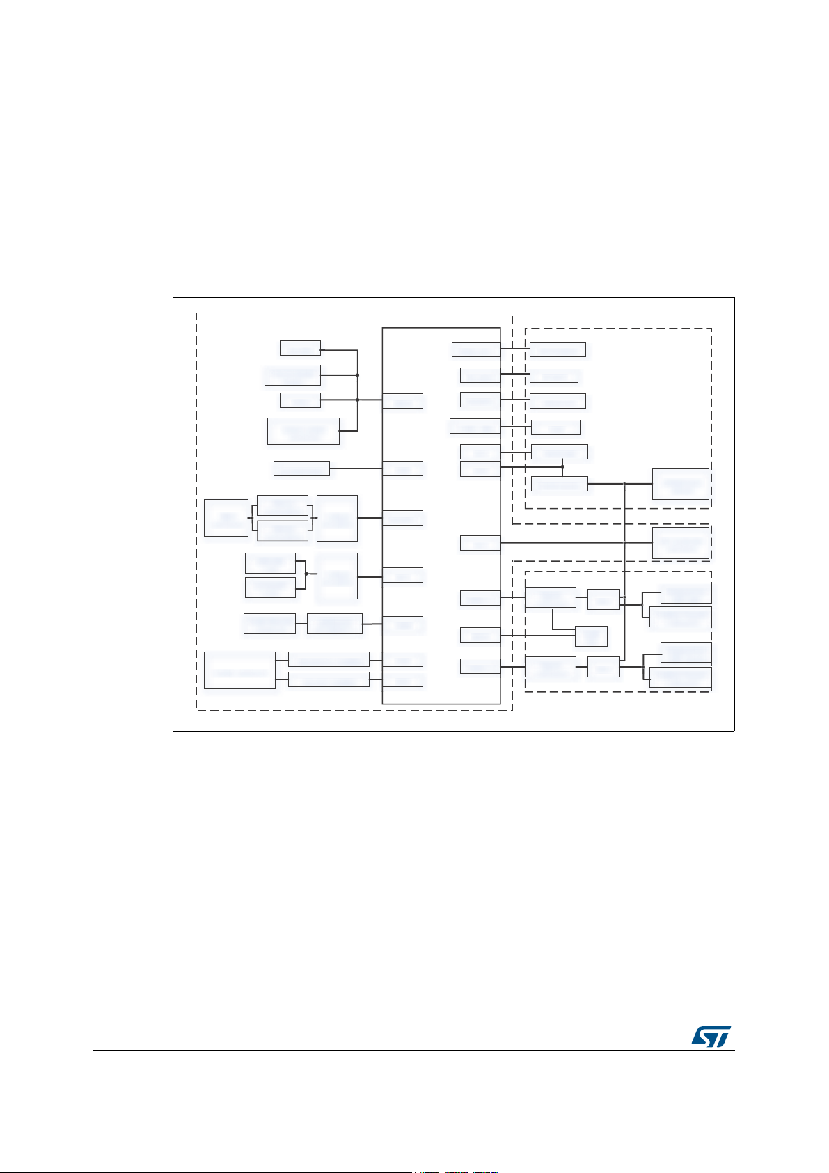
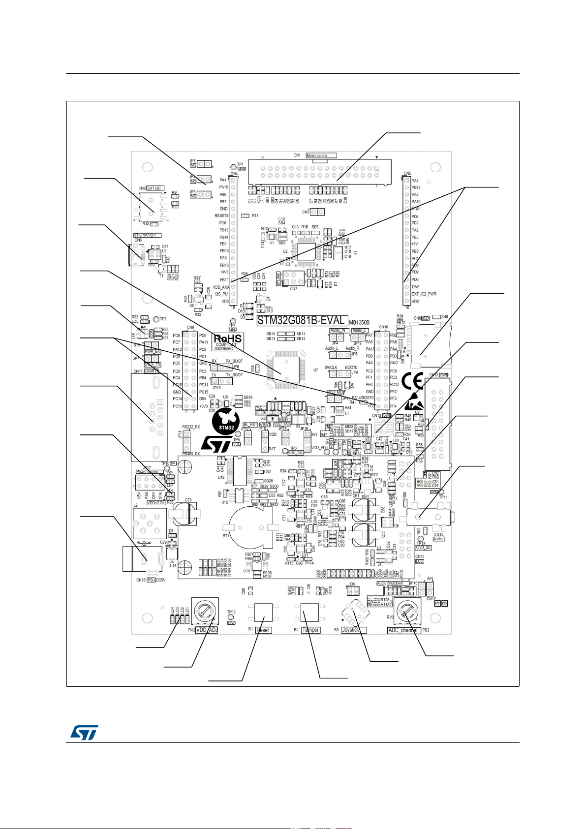
8 Hardware layout and configuration
The STM32G081B-EVAL Evaluation board is designed around the STM32G081RBT6 (64pin LQFP package). The hardware block diagram
between STM32G081RBT6 and peripherals (motor control connector, RS232, RS485,
Audio DAC, microphone ADC, TFT LCD, CAN, IrDA, IR LED, IR receiver, LDR, MicroSD
card, CEC on two HDMI connectors, Smartcard slot, Temperature sensor… etc.) and
Figure 4 help users to locate these features on the Evaluation board.
Figure 3. Hardware block diagram
Figure 3 illustrates the connection
12/78 UM2403 Rev 1
Page 13
UM2403 Hardware layout and configuration
06Y9
-3PRWRUFRQWURO
VLJQDOVHOHFWLRQ
&1PRWRUFRQWURO
FRQQHFWRU
&1&1
GDXJKWHUERDUG
FRQQHFWRUV
&1PLFUR6'FDUG
&16:'
FRQQHFWRU
&16:'
FRQQHFWRU
&1DXGLRMDFN
&17)7/&'
59
SRWHQWLRPHWHU
%
MR\VWLFN
%
WDPSHUEXWWRQ
%
UHVHWEXWWRQ
59
9''DGMXVWPHQW
XVHU/('V
&1SRZHUMDFN
/'
ORZYROWDJH
DODUP/('
&1
86$57
&1&1
H[WHQVLRQKHDGHU
8
670*5%7
&1
67/,1.9
86%
&1
H[WHQVLRQ,&
FRQQHFWRU
/'
67/,1.9
&20/('
Figure 4. STM32G081B-EVAL Evaluation board layout
UM2403 Rev 1 13/78
77
Page 14
Hardware layout and configuration UM2403
06Y9
&1
+'0,VRXUFH
&1
+'0,VLQN
5/'5
&1
VPDUWFDUG
/',5/('
',5UHFHLYHU
06Y9
&1
7\SH&'53
GXDOUROHSRUW
&1
'LVSOD\3RUW
LQSXW
&1
86%FRQQHFWRU
&1
H[WHQVLRQSRZHU
LQSXW
&1
'LVSOD\3RUW
RXWSXW
&1
86%7\SH$
&1
7\SH&VLQN
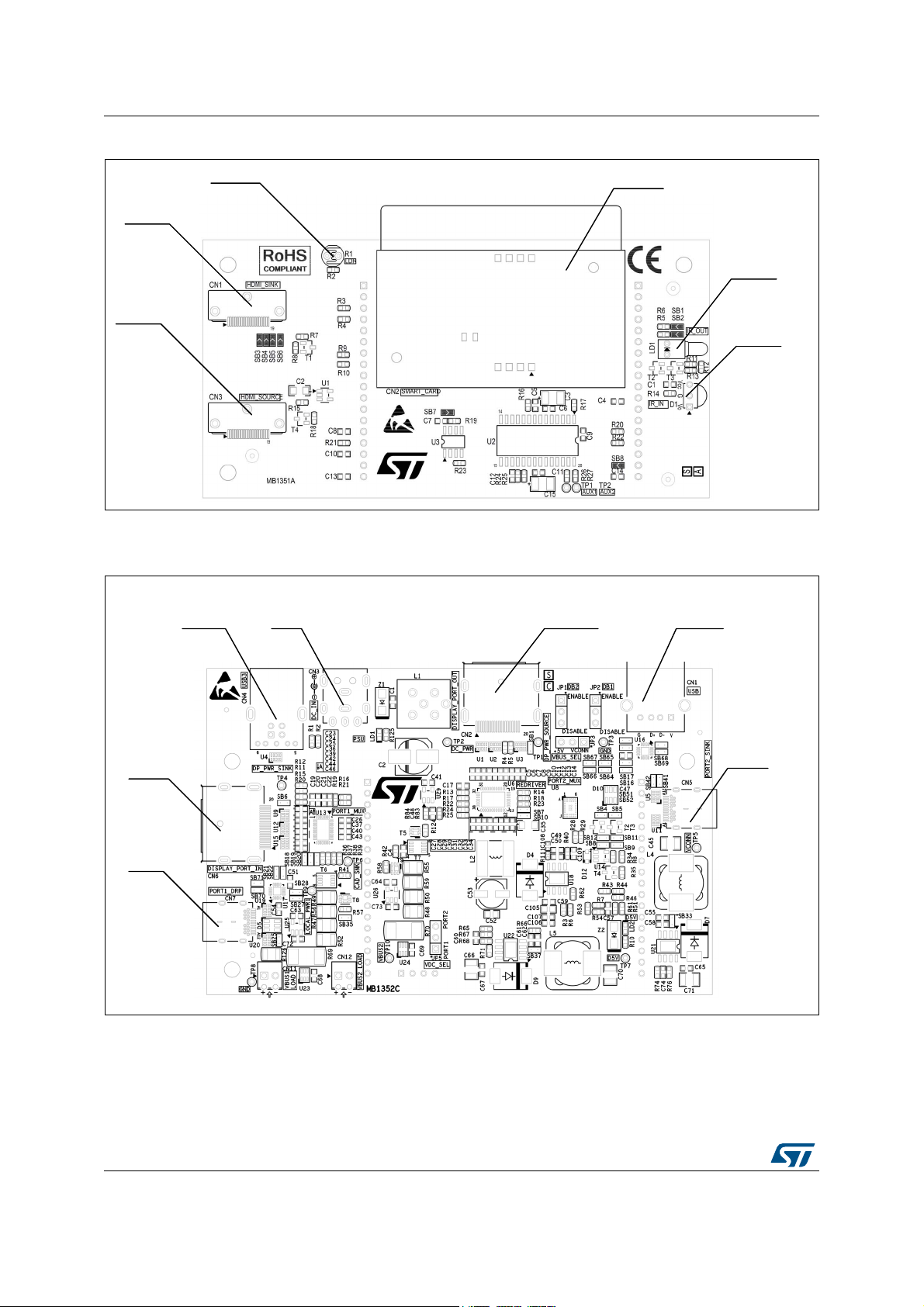
Figure 5. Legacy peripheral daughterboard
Figure 6. USB Type-C and Power Delivery daughterboard
14/78 UM2403 Rev 1
Page 15
UM2403 Hardware layout and configuration
8.1 Embedded ST-LINK/V2-1
The ST-LINK/V2-1 programming and debugging tool is integrated on the STM32G081BEVAL Evaluation board. Compared to ST-LINK/V2 the changes are listed below.
The new features supported on ST-LINK/V2-1 are:
• USB software enumeration
• Virtual COM port interface on USB
• Mass storage interface on USB
• USB power management request for more than 100 mA power on USB
This feature is no longer supported on ST-LINK/V2-1:
• SWIM interface
For all general information concerning debugging and programming features common
between V2 and V2-1 refer to ST-LINK/V2 in-circuit debugger/programmer for STM8 and
STM32 User manual (UM1075) in the www.st.com website.
Note: It is possible to power the board via CN6 (Embedded ST-LINK/V2-1 USB connector) even if
an external tools is connected to CN12 or CN13 (External SWD connector).
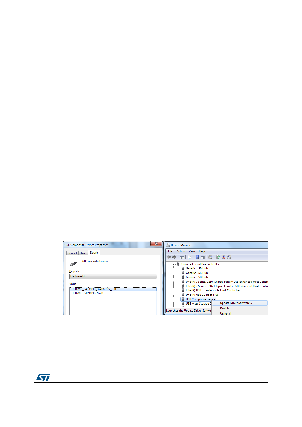
8.1.1 Drivers
The ST-LINK/V2-1 requires a dedicated USB driver, which can be found on www.st.com for
Windows PC (7, 8 or 10).
In case the STM32G081B-EVAL Evaluation board is connected to the PC before the driver
is installed, some STM32G081B-EVAL interfaces may be declared as “Unknown” in the PC
device manager. In this case, the user must install the driver files, and update the driver of
the connected device from the device manager.
Note: Prefer using the “USB Composite Device” handle for a full recovery.
Figure 7. USB Composite Device
8.1.2 ST-LINK/V2-1 firmware upgrade
The ST-LINK/V2-1 embeds a firmware upgrade mechanism for in-situ upgrade through the
USB port. As the firmware may evolve during the lifetime of the ST-LINK/V2-1 product (for
example new functionality, bug fixes, support for new microcontroller families), it is
recommended to visit the www.st.com website before starting to use the STM32G081B-
EVAL board and periodically, to stay up-to-date with the latest firmware version.
UM2403 Rev 1 15/78
77
Page 16

Hardware layout and configuration UM2403
8.2 Power supply
The STM32G081B-EVAL Evaluation mother board is designed to be powered by 5 V DC
power supply and is protected by PolyZen from wrong power plug-in event. It is possible to
configure the mother board to use any of the following four sources for the power supply:
• 5 V DC power adapter connected to CN16, the power Jack on the board (Power
Supply Unit on silk screen of JP17 (PSU)). The external power supply is not provided
with the board.
• 5 V DC power with 500 mA limitation from CN6, the USB Micro-B connector of
STLINK/V2-1 (USB 5 V power source on silkscreen of JP17 (STlk)). If the USB
enumeration succeeds, the ST-LINK U5V power is enabled, by asserting the PWR_EN
pin. This pin is connected to a power switch, which powers the board. This power
switch features also a current limitation to protect the PC in case of short-circuit on the
board. If overcurrent (more than 500 mA) happens on the board, the LED LD5 lights
up.
• 5 V DC power from CN6 directly, the USB Micro-B connector of STLINK/V2-1 (USB 5 V
power source on silkscreen of JP17 (U5V)).
• 5 V DC power from CN5 or CN9, the extension connector for daughterboard power
source (D5V) on silkscreen of JP19).
The UCPD daughterboard uses its own 19V power adapter to support USB PD, in this case
the mother board uses D5V from the UCPD daughterboard to supply all circuits on
STM32G081B-EVAL Evaluation board. D5V of the UCPD daughterboard has three sources
as below:
• 19 V DC power adapter connected to CN3 on the UCPD daughterboard
• Power from Type-C Port1 CN7 on the UCPD daughterboard
• Power from Type-C port2 CN5 on the UCPD daughterboard
19 V DC power adapter and Type-C Port1 sources are automatically selected by circuit (D8
and T10 on the UCPD daughterboard). Refer to Table15 for detail.
16/78 UM2403 Rev 1
Page 17
UM2403 Hardware layout and configuration
06Y9
3RZHUMDFNRQPRWKHUERDUG
9
67/,1.986%
9
'9SLQRQ&1&1
9
3RZHU
VZLWFK
'&
'&
3RZHUMDFNRQ86%ERDUG9
9
0RWKHUERDUG
86%&GDXJKWHUERDUG
-3
368
67ON
89
'9
7\SH&3257
7\SH&3257
-3'
3257
3257
7
Figure 8. 5 V power structure
The STM32G081B-EVAL Evaluation board can be powered from the ST-LINK/V2-1 USB
connector CN6 with a PC, but only the ST-LINK/V2-1 circuit has the power before USB
enumeration, because the host PC only provides 100
the USB enumeration, the STM32G081B-EVAL board requires 300
PC. If the host is able to provide the required power, the enumeration succeeds, the power
transistor U5 is switched ON, the red LED LD7 is turned ON, and thus the STM32G081BEVAL board is powered and can consume maximum 300 mA current. If the host PC is not
able to provide the requested current, the enumeration fails. Therefore the STM32 part
including the extension board is not powered. As a consequence the red LED LD7 remains
turned OFF. In this case it is mandatory to use an external power supply to supply extra
power.
E5V (from PSU) or D5V can be used as external power supply in case current consumption
of the STM32G081B-EVAL board exceeds the allowed current on USB. In this condition it is
still possible to use USB for communication, for programming or debugging only, but it is
mandatory to power the board first using E5V or D5V, and then connecting the USB cable to
the PC. Proceeding this way ensures that the enumeration succeeds thanks to the external
power source.
The following power sequence procedure must be respected:
mA to the boards at that time. During
mA power from the host
UM2403 Rev 1 17/78
77
Page 18

Hardware layout and configuration UM2403
89
368
'9 67ON
89
368
'9 67ON
89
368
'9 67ON
89
368
'9 67ON
1. Connect jumper JP17 for PSU or D5V side
2. Check that JP5 is removed
3. Connect the external power source to PSU or D5V (daughterboard mounted)
4. Check red LED LD7 is turned ON
5. Connect the PC to USB connector CN6
If this order is not respected, the board may be powered by VBUS first then E5V or D5V,
and the following risks may be encountered:
1. If more than 300 mA current is needed by the board, the PC may be damaged or
current can be limited by PC. As a consequence the board is not powered correctly.
2. 300 mA is requested at enumeration (since JP5 must be OFF), so there is risk that
request is rejected and enumeration does not succeed if PC can't provide such current.
Consequently the board is not powered (LED LD7 remains OFF).
In case the STM32G081B-EVAL board is powered by an USB charger through CN6, there is
no USB enumeration needed. User can set JP17 to U5V to allow the board to be powered
anyway from CN6.
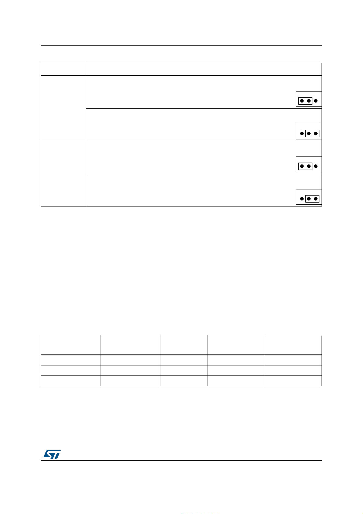
The power source is selected by setting the related jumpers JP17, JP15 and JP16 as
described in table 2.
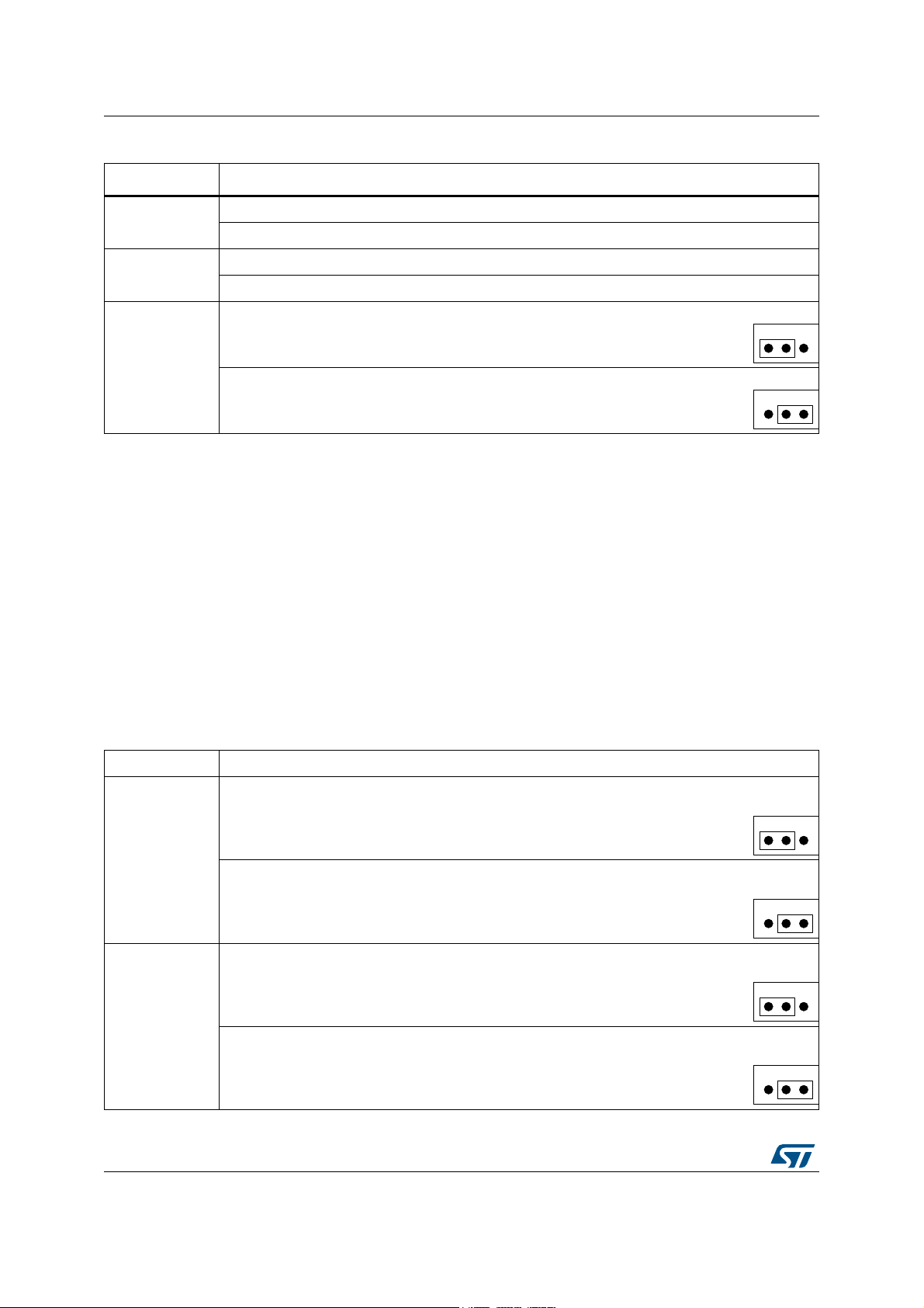
Table 2. Power source related Jumpers
Jumper Description
JP17 is used to select one of the four possible power supply resources.
Only for power supply from USB (CN6) of ST-LINK/V2-1 to STM32G081B-EVAL, JP17 is set as
shown on the right:
Only for power supply from the daughterboard connectors(CN5 or CN9) to STM32G081BEVAL, JP17 is set as shown on the right: (default Setting)
JP17
Only for power supply jack(CN16) to the STM32G081B-EVAL, JP17 is set as shown on the
right:
Only for power supply from USB (CN6) to STM32G081B-EVAL without current limited, JP17 is
set as shown on the right:
18/78 UM2403 Rev 1
Page 19
UM2403 Hardware layout and configuration
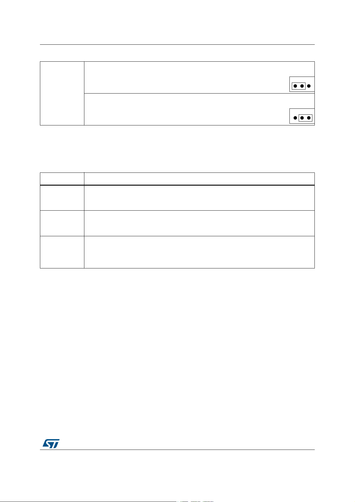
Table 2. Power source related Jumpers (continued)
Jumper Description
The Vbat pin of STM32G081RBT6 is connected to VDD when JP15 is set as shown on the right
(default setting):
JP15
The Vbat pin of STM32G081RBT6 is connected to 3V battery when JP15 is set as shown on the
right:
The VDD pin of STM32G081RBT6 is connected to 3.3V when JP16 is set as shown on the right
(default setting), when the UCPD daughterboard is used, this setting is mandatory:
JP16
The VDD pin of STM32G081RBT6 is connected to VDD_ADJ when JP16 is set as shown on the
right:
Note: The VDD_MCU Idd measurement can be done by current meter which mounted on JP11
when it is open. But JP11 is not allowed to be opened without current meter; otherwise
STM32G081RBT6 would be damaged due to lacking of power supply on its power pins.
Note: LD8 is lit when VDD < 2.7 V and in this case IOs and some Analog IPs of STM32G081RBT6
work with degraded performances.
Note: The UCPD daughterboard works with VDD=3.3V, so it is mandatory to close JP16 pin1 and
pin2.
The LED LD7 is lit when the STM32G081B-EVAL Evaluation board is powered by the 5V
correctly.
Tab le 3 shows the low voltage limitations that might apply depending on the characteristics
of some peripheral components. Components might work incorrectly when the power level
is lower than the limitation.
Board peripheral component IO name
Mother board Audio amplifier U17 Audio input 2.2V
Mother board Microphone amplifier U12 Audio output 2.7V
Legacy daughterboard Smartcard CN2 USART1 2.7V
Table 3. Low voltage limitation
UM2403 Rev 1 19/78
Low voltage
limitation
77
Page 20
Hardware layout and configuration UM2403
8.3 Clock references
Two clock sources are available on STM32G081B-EVAL Evaluation board for
STM32G081RBT6 and RTC embedded.
• X2, 32KHz Crystal for embedded RTC
• X3, 8MHz Crystal for the STM32G081RBT6 microcontroller, it can be disconnected by
removing R45 and R46 when internal RC clock is used
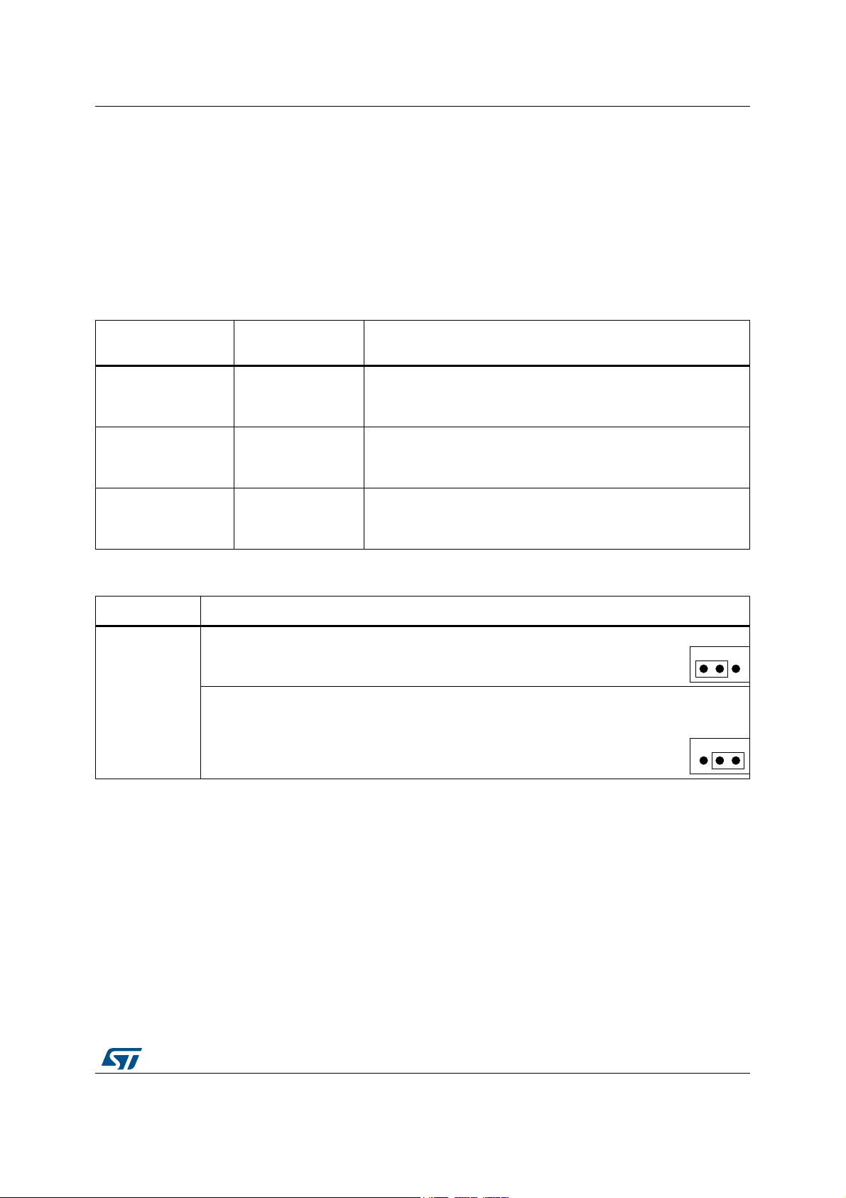
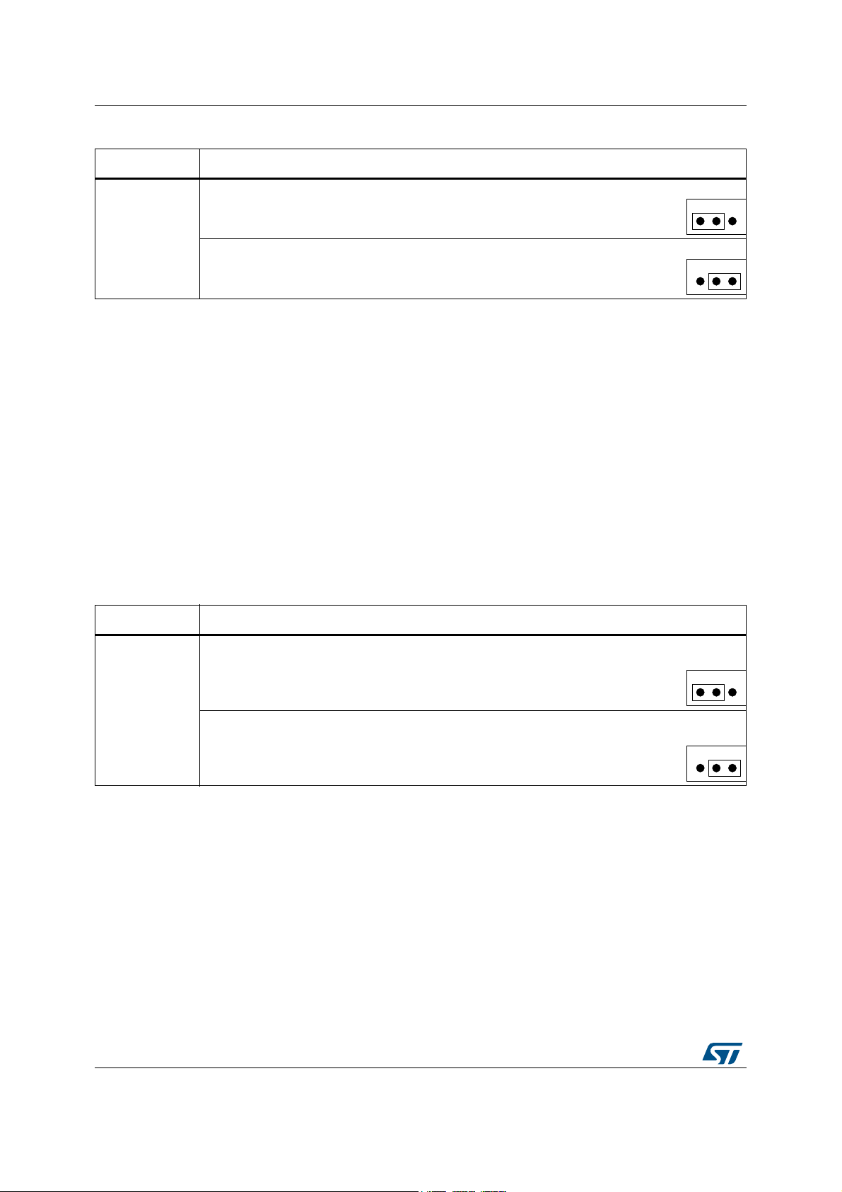
Jumper Description
PC14 is connected to 32KHz crystal when SB18 is open (default setting).
SB18
SB19
PC14 is connected to extension connector CN9 when SB18 is closed. In such case R43 must be
removed to avoid disturbance due to the 32Khz quartz.
PC15 is connected to 32KHz crystal when SB19 is open (default setting).
PC15 is connected to extension connector CN9 when SB19 is closed. In such case R44 must be
removed to avoid disturbance due to the 32Khz quartz.
Table 4. 32 KHz crystal X2 related solder bridges
Jumper Description
PF0 is connected to 8MHz crystal when SB20 is open (default setting).
SB20
SB21
PF0 is connected to extension connector CN10 when SB20 is closed. In such case R45 must be
removed to avoid disturbance due to the 8Mhz quartz.
PF1 is connected to 8MHz crystal when SB21 is open (default setting).
PF1 is connected to extension connector CN10 when SB21 is closed. In such case R46 must be
removed to avoid disturbance due to the 8Mhz quartz.
Table 5. 8 MHz crystal X3 related solder bridges
8.4 Reset source
The general reset of the STM32G081B-EVAL Evaluation board is active low and the reset
sources include:
• Reset button B1
• Debugging Tools from SWD connector CN12 and CN13
• Daughterboard from CN4
• Embedded ST-LINK/V2-1
• RS232 connector CN11 for ISP.
Note: The jumper JP12 to be closed for RESET handled by pin8 of RS232 connector CN11 (CTS
signal), please refer to
Section 8.6.2 for detail.
20/78 UM2403 Rev 1
Page 21
UM2403 Hardware layout and configuration
8.5 Boot Option
The STM32G081B-EVAL Evaluation board is able to boot from:
• Embedded User Flash
• System memory with boot loader for ISP
• Embedded SRAM for debugging
The boot option is configured by closing JP9 pin2-3 and setting one jumper cap on CN10
among pin 17, pin 19 and pin 21 and one option bit (see
Table 6. Boot related jumper
Table 6 and Tab le 7).
Jumper
configuration
Bit25 in USER
OPTION BYTES
CN10 pin 19 and
pin 17 closed by
X STM32G081B-EVAL boot from User Flash (default setting)
jumper
CN10 pin 19 and
pin 21 closed by
0 STM32G081B-EVAL boot from Embedded SRAM
jumper
CN10 pin 19 and
pin 21 closed by
1 STM32G081B-EVAL boot from System Memory
jumper
Table 7. Boot0 related jumpers
Jumper Description
PA14-BOOT0 is used as SWCLK when JP9 is set as shown on the right (default setting).
JP9
The Bootloader_BOOT0 is managed by pin 6 of connector CN11 (RS232 DSR signal) and it is
connected to PA14-BOOT0 when JP9 is set as shown on the right. This configuration is used for
boot loader application only.
Boot from
8.6 Peripherals on mother board
8.6.1 Audio
The STM32G081B-EVAL Evaluation board supports stereo audio playback and microphone
recording by an external headset connected on audio jack CN15. Audio play is connected to
DAC output of STM32G081RBT6 through an audio amplifier and microphone on headset is
connected to ADC input of STM32G081RBT6 through a microphone amplifier. Audio
amplifier can be enabled or disabled by setting of JP18 and mono/stereo playback can be
chosen by setting of JP6, refer to
Tabl e 8 for detail.
UM2403 Rev 1 21/78
77
Page 22
Hardware layout and configuration UM2403
Table 8. Audio related jumpers
Jumper Description
Speaker amplifier U17 is enabled when JP18 is closed (default setting)
JP18
Speaker amplifier U17 is disabled when JP18 is open
PA4 is connected to VIN1 of Audio amplifier when JP19 is closed (default setting)
JP19
PA4 is disconnected to VIN1 of Audio amplifier when JP19 is open
Mono playback is enabled when JP6 is set as shown on the right (default setting):
JP6
Stereo playback is enabled when JP6 is set as shown on the right:
Audio amplifier operates correctly when VDD > 2.2 V and microphone amplifier operates
correctly when VDD > 2.7
V.
8.6.2 RS232 and RS485
Communication through RS232 (with Hardware flow control CTS and RTS) and RS485 is
supported by D-type 9-pins RS232/RS485 connector CN11, which is connected to USART1
of STM32G081RBT6 on STM32G081B-EVAL Evaluation board. The signal
Bootloader_RESET (shared with CTS signal) and Bootloader_BOOT0 (shared with DSR
signal) are added on RS232 connector CN11 for ISP support.
By default, PC4 and PC5 are connected as TX and RX signals. PA9 and PA10 are also can
be connected as these two signals for bootloader which is NOT supported on PC4 and PC5
by setting of jumpers in
Jumper Description
RS232_RX is connected to RS232 transceiver and RS232 communication is enabled when
JP14 is set as shown on the right (default setting):
JP14
RS485_RX is connected to RS485 transceiver and RS485 communication is enabled when
JP14 is set as shown on the right:
PC4 is connected as TX signal without bootloader being supported when JP10 is set as shown
on the right (Default setting):
JP10
PA9 is connected as TX signal with bootloader being supported when JP10 is set as shown on
the right (CN1 motor control connector is needed to be open in this case):
Table 9.
Table 9. RS232 and RS485 related jumpers
22/78 UM2403 Rev 1
Page 23
UM2403 Hardware layout and configuration
Table 9. RS232 and RS485 related jumpers (continued)
PC5 is connected as RX signal without bootloader being supported when JP8 is set as shown
on the right (default setting):
JP8
PA10 is connected as RX signal with bootloader being supported when JP8 is set as shown on
the right (in this case, CN1 motor control connector must be open):
The RS485 communication is supported by RS485 transceiver ST3485EBDR which
connected to pin4 and pin9 of D-type 9-pins connector CN11 (share same connector with
USART1).
Jumper Description
The external failsafe biasing are enabled when solder bridges SB29 and SB31 was closed
SB29,SB31
Default Setting: Not fitted
The bus termination is enabled when solder bridge SB32 is closed.
SB32
Default Setting: Not fitted
The AC termination is disabled when solder bridge SB30 is closed for high baud rate
SB30
communication.
Default Setting: Not fitted
Table 10. RS485 related solder bridges
8.6.3 microSD card
The 8-GB (or more) microSD card connected to SPI1 port (shared with color LCD) of
STM32G081RBT6 is available on the board. microSD card detection is managed by
standard IO port PC9 and it must be set with internal pull-up.
8.6.4 Analog Input
The two-pin header CN17 and 10K ohm potentiometer RV3 was connected to PB2 of
STM32G081RBT6 as analog input. A low pass filter can be implemented by replacing of
R111 and C90 with right value of resistor and capacitor as requested by end user's
application.
8.6.5 External I2C Connector
The I2C1 bus of the STM32G081RBT6 is connected to CN2 on the STM32G081B-EVAL.
The I2C functional daughterboard can be mounted on the CN2 connector and accessed by
the microcontroller through the I2C1 bus, it shares same I2C1 bus with Temperature sensor
U3 and DDC on HDMI_Source connector CN3 on legacy peripheral daughterboard.
The pull up voltage level of I2C1 bus is automatically decided by the daughterboard (the
legacy peripheral daughterboard or the UCPD daughterboard) on CN4 and CN5. If there is
UM2403 Rev 1 23/78
77
Page 24
Hardware layout and configuration UM2403
no daughterboard on these connector, pin17 must be closed to pin18 on both CN4 and CN5
by jumpers. Thus I2C pull up voltage and reset pull up voltage on CN2 would be the voltage
of VDD.
8.6.6 Motor Control
The STM32G081B-EVAL Evaluation board supports both asynchronous and synchronous
three-phase brushless motor control via a 34-pins connector CN1, which provides all
required control and feedback signals to and from motor power-driving board.
Available signals on this connector includes emergency stop, motor speed, 3 phase motor
current, bus voltage, power heatsink coming from the motor driving board and 6 channels of
PWM control signal going to the motor driving circuit.
Daughterboard on CN4 and CN5 must be removed and some jumpers set for motor control
application:
• Close JP1, JP2 and JP3.
• Open JP4 and JP6.
• Open pin2-3 of JP8 and JP10.
8.6.7 Display and Input devices
The 2.4" color TFT LCD connected to SPI1 port of STM32G081RBT6 and 4 general
purpose color LED's (LD 1,2,3,4) are available as display device. The 4-direction joystick
(B3) with selection key which connected to PA0 and supports wakeup feature. Tamper
button (B2) are also available as input devices.
Pin Description Pin connection Pin Description Pin connection
1 CS PB8 9 VDD 3.3V
2 SCL PB3 10 VCI 3.3V
3SDI PA7 11GND GND
4RS - 12GND GND
5 WR - 13 BL_VDD 5V
6 RD - 14 BL_Control 5V
7 SDO PB4 15 BL_GND GND
8 RESET RESET# 16 BL_GND GND
Table 11. LCD modules
2.4” TFT LCD connector CN14
Note: The bi-directional voltage translator is implemented on SPI MOSI signal between
STM32G081RBT6 and LCD to support 3-wires serial interface of LCD panel only supports
3-wire SPI port. The direction of this voltage translator is controlled by IO PC12 (the IO PA7
is working as MOSI when PC12 is high or as MISO when PC12 is LOW).
24/78 UM2403 Rev 1
Page 25

UM2403 Hardware layout and configuration
8.7 Peripherals on legacy peripheral daughterboard
8.7.1 LDR (Light dependent resistor)
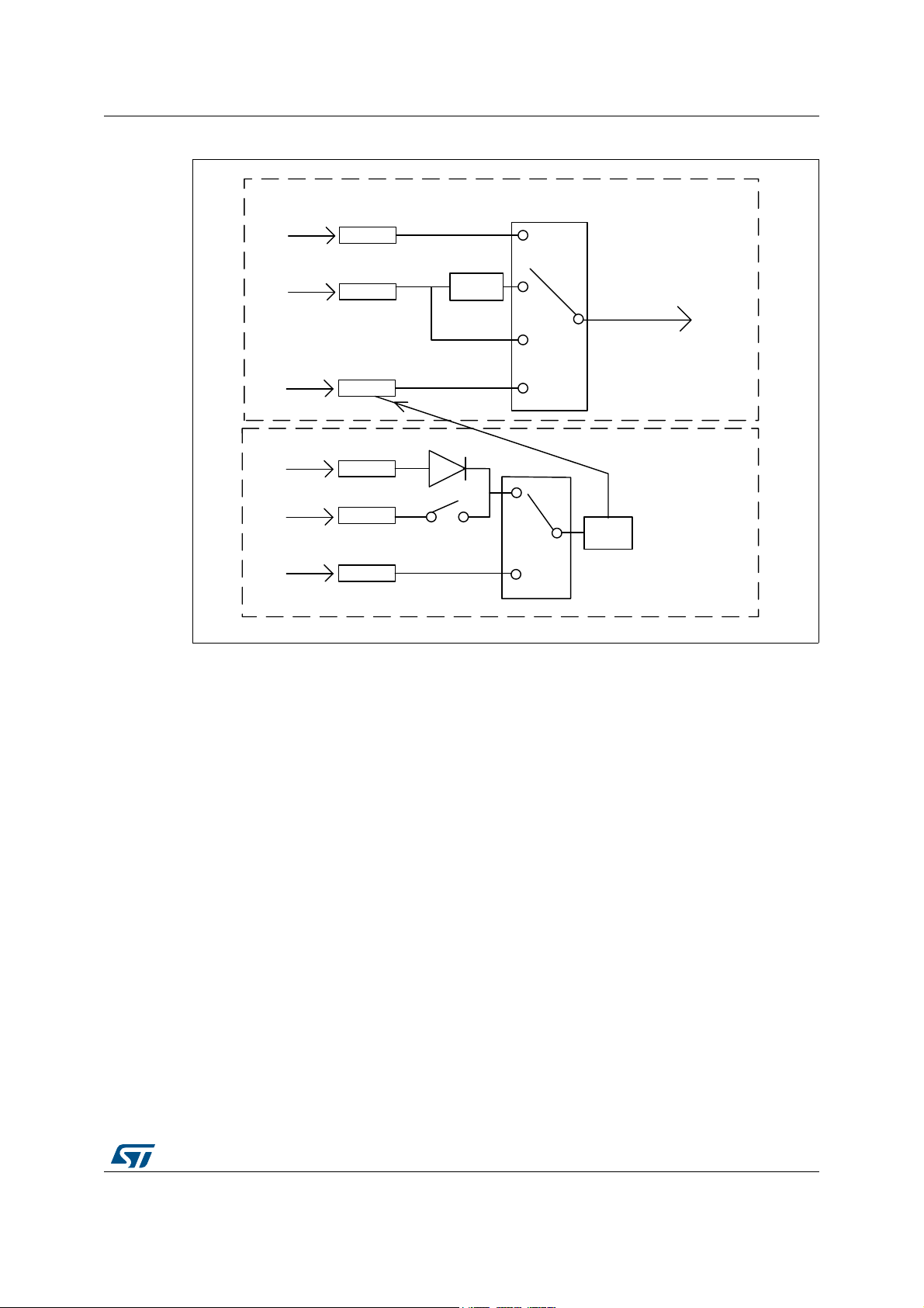
The VDD is divided by resistor bridge of LDR VT9ON1 and 8.2 K resistor and connected to
PA1 (COM1_IN+/ADC IN1) as shown
Figure 9 on STM32G081B-EVAL Evaluation board.
Figure 9. GP comparator 1
It's possible to compare LDR output with ¼ band gap, 1/2 band gap, 3/4 band gap, band
gap and DAC1 OUT and to connect LDR output to ADC IN1 for AD conversion.
8.7.2 Temperature sensor
A temperature sensor STLM75M2F is connected to the I2C1 bus of the STM32G081RBT6,
and shares same I2C1 bus with EXT I2C connector (on mother board) and DDC on
HDMI_Source connector CN3 (on legacy board).
I2C address of temperature sensor is 0b100100(A0), A0 can be 0 or 1 depends on the
setting of SB7.
Solder Bridge Description
SB7
Note: The temperature result measured from STLM75M2F would be a little higher than the
ambient temperature due to the power dissipation of components on the board.
Table 12. Temperature sensor related solder bridge
I2C address A0 is 0 when SB7 is open.
(Default setting)
I2C address A0 is 1 when SB7 is closed.
UM2403 Rev 1 25/78
77
Page 26

Hardware layout and configuration UM2403
8.7.3 Smartcard
STMicroelectronics smartcard interface chip ST8024L is used on STM32G081B-EVAL
Evaluation board for asynchronous 1.8V, 3V and 5V smartcards. It performs all supply
protection and control functions based on the connections with STM32G081RBT6 listed in
Tab le 13.
Table 13. Connection between ST8024L and STM32G081RBT6
Signals of
ST8024L
5V/3V Smartcard power supply selection pin PB15
I/OUC MCU data I/O line PA2
XTAL1 Crystal or external clock input PD4
OFF Detect card presence, Interrupt to MCU PB12
RSTIN Card reset input from MCU PA15
CMDVCC Start activation sequence input (Active Low) PB0
1.8V
Smartcard operates correctly when VDD > 2.7 V.
8.7.4 HDMI CEC
Two HDMI connectors CN1 and CN3 are available on STM32G081B-EVAL legacy
peripheral daughterboard.
• The connector CN1 is HDMI sink connector with
– DDC connected to I2C2 of STM32G081RBT6
– HPD controlled by IO PD2 through transistor T1
– CEC connected to PB10 through transistor T4
• The connector CN3 is HDMI source connector with
– DDC connected to I2C1 of STM32G081RBT6 and shared with Temperature
sensor and EXT I2C connector
– HPD controlled by IO PD3
– CEC connected to PB10 through transistor T4
– HDMI 5V powered by power switch U1
Description
CC operation selection. Logic high selects 1.8 V
1.8 V V
operation and overrides any setting on the 5V/3V pin.
Connect to
STM32G081RBT6
PA3
The signals TDMS D+[0..2], TDMS_CLK+, TDMS D-[0..2], TDMS_CLK- on these two HDMI
connectors are connected together.
The CEC injector mode can be enabled by some PCB reworks for debugging purpose only:
• Remove resistors R3, R4, R7, R9, R10, R15 and R22.
• Close solder bridges SB3, SB4, SB5 and SB6.
Note: The I/O PD2 must be set in open-drain output mode by firmware when working as an HPD
signal control on the HDMI sink connector CN1.
26/78 UM2403 Rev 1
Page 27

UM2403 Hardware layout and configuration
8.7.5 IR LED and IR receiver
The IR receiver TSOP34836 is connected to PC6 of STM32G081RBT6 and a current
around 100mA on IR LED is driven by PB9 through transistors T2 and T3 on the board.
Note: IR LED may be driven by PB9 directly with 20mA current when SB1 is closed and SB2 is
open.
8.8 USB Type-C and Power Delivery daughterboard
The UCPD daughterboard is a development platform composed of STM32G081B-EVAL
Evaluation board. This daughterboard is used for demonstrating the functionalities of the
USB Type-C and USB Power Delivery (USB PD) technologies, facilitating the users to
develop their solutions. Refer to
Note: The USB PD reference design on the UCPD daughterboard is used to demonstrate the
capability of STM32G081RBT6. This USB PD circuit may not pass all USB PD certifications.
Note: The UCPD daughterboard works with VDD=3.3V. So JP16 pin1-2 must be closed on mother
board.
Note: The UCPD daughterboard conflicts with legacy peripheral daughterboard and Motor control
on STM32G081B-EVAL Evaluation board.
Figure 3 for daughterboard structure.
8.8.1 USB Type-C receptacles
Two USB Type-C certified receptacles CN7 and CN5 are present on the UCPD
daughterboard, representing respectively the PORT 1 and PORT 2. PORT 1 can be used as
DRP (Dual-Role Port), which is eligible to supply another platform plugged by a USB
Type-C cable when they are configured as Provider or, otherwise, to be supplied in case of
Consumer configuration. PORT 2 can only be used as SINK.
Video signals on display port input connector (CN6) and data signals on USB3.1 Gen1
Type-B connector (CN4) are multiplexed on Type-C PORT 1 thanks to a crosspoint switch
IC TUSB546-DCI. These signals on CN6 or on CN4 have to be generated by an external
computer or notebook to evaluate the alternate mode (AM) capability of the USB PD
technology. The crosspoint switch can be configured through I2C bus, and its I2C address is
0b1000100. The cable which is plugged into CN4 can be detected by PA15.
Same as Type-C PORT1, video signals on display port output connector (CN2) are
connected to Type-C PORT 2 through another crosspoint switch IC CBTL08GP053 and
DisplayPort Linear Redriver IC SN65DP141. I2C address of CBTL08GP053 is 0b0110000
and SN65DP141's default I2C address is 0b0000000. A Type-A receptacle's (CN1) D+ and
D- signals are also connected to Type-C PORT 2 directly. Its VBUS can be set by JP3 in
Tab le 14.
UM2403 Rev 1 27/78
77
Page 28
Hardware layout and configuration UM2403
Table 14. VBUS related jumpers
Jumper Description
VBUS is connected to VCONN when JP3 is set as shown on the right (default setting).
JP3
VBUS is connected to D5V through mother board when JP3 is set as shown on the right.
Note: Some week USB charger can not provide power to board immediately from port1 Type-C
receptacle when external 19V power adapter is plugged off. If board lose power and reset
during such use case, close JP6 may help to solve this problem. JP6 is open by default.
8.8.2 Power Delivery and local power management
The UCPD daughterboard has its own external power jack (CN3, 19V/4A input) to support
power delivery function and to provide up to 15V/3A on Type-C port1 (CN7).
The STM32G081B-EVAL Evaluation board can be powered by D5V from the UCPD
daughterboard as shown in
by three resources, 19V from external power jack, VBUS on Port 1 and VBUS on Port 2. A
circuit is implemented on the UCPD daughterboard to automatically select external 19V
power supply or VBUS on Port1, because external 19V and VBUS on Port1 are the two
power sources for Port1 to D5V. A jumper JP5 is used to select D5V resources in
Table 15. Local power related jumpers
Figure 5. D5V on the UCPD daughterboard can be generated
Tab le 15.
Jumper Description
D5V from the UCPD daughterboard is generated from external 19V or VBUS on Port1 when JP5
is set as shown on the right (default setting).
JP5
D5V from the UCPD daughterboard is generated from VBUS on Port2 when JP5 is set as shown
on the right.
8.8.3 VBUS management and discharge mechanism
Type-C port1 (CN7) can be used as DRP (Dual-Role Port), its VBUS can be managed for
supplying other platforms as Provider, or to be supplied as Consumer. Two MOSFETs T6
and T7 are set in back-to-back configuration to protect and isolate the VBUS supplying path
on both directions.
If the CN7 acts as Provider, the VBUS is on the supply path by mean of the discrete load
switch (T6 and T7) driven by the STM32G081RBT6 (GPIO, PD3). For the Consumer case,
the same VBUS path is managed by PD3 of STM32G081RBT6 enabling the discrete load
switch.
All power profiles are listed in Tab le 16.
28/78 UM2403 Rev 1
Page 29

UM2403 Hardware layout and configuration
CN7 role
Provider
Consumer -
Table 16. VBUS Power Delivery profiles
Solder bridges
setting
SB2, SB3, SB23,
SB26 ON
SB13, SB14, SB15
OFF
SB13, SB14, SB15
ON
SB2, SB3, SB23,
SB26 OFF
Power level
PWM Mode:
PWM voltage-3A
GPIO Mode:
5V / 9V / 15V- 3A
Decided by Provider
which is connected
through Type-C cable
Source
control
signal
PD3 High PC1-PWM signal
PD3 High
PD3 low -
Voltage control signal
5V: PC1(VSOURCE9V) and
PA1(VSOURCE-15V)
tristate
9V: PC1(VSOURCE9V) low
15V: PA1 (VSOURCE15V) low
Moreover, the VBUS path on PORT1 presents a discharge mechanism implemented by the
MOSFET T8 and an RC filter and controlled by PB13, and the VBUS path on PORT2
presents a discharge mechanism implemented by the MOSFET T9 and an RC filter and
controlled by PB14.
8.8.4 VBUS voltage-sensing and current-sense stage
Each Type-C port is equipped by a voltage-sensing and a current-sensing stage which are
matched with the voltage sensing carried by the STM32G081RBT6 ADC peripherals. Refer
to
Table 17 for detail. They are able to monitor the right power level applied on the port
VBUS.
PORT VSENSE ADC ISENSE ADC
PORT 1 PB1 ADC_IN9 PB10 ADC_IN11
PORT 2 PA3 ADC_IN3 PB12 ADC_IN16
Table 17. Voltage-sensing and current-sensing ADC
8.8.5 CC management
Dead battery, VCONN output and fast role swap functions are supported on CC signal of
Type-C PORT 1.
1. Dead battery enable
Dead battery function is supported by OVP chip U17 and U16. And this function also
UM2403 Rev 1 29/78
77
Page 30

Hardware layout and configuration UM2403
embedded in STM32G081RBT6. When OVP part U17 is bypassed, dead battery
function in STM32G081RBT6 can be enable or disable through enable signals by set
JP2 (CC1) or JP1 (CC2). Refer to
Jumper Description
Embed dead battery function is enable when JP1 is set as shown on the right (default setting).
Table 18. Dead battery related jumpers
Tabl e 18 for detail.
JP1
JP2
Embed dead battery function is disable when JP1 is set as shown on the right.
Embed dead battery function is enable when JP2 is set as shown on the right (default setting).
Embed dead battery function is disable when JP2 is set as shown on the right.
2. VCONN output control
When the full-featured cable is connected to PORT 1, the VCONN is directly managed by
the STM32G081RBT6 by mean of the PD4 or PB9 and the load switches STMPS2161 U10
and U14.
3. Fast role swap
Type-C PORT 1 can be configure to action fast role swap managed by STM32G081RBT6
through PA2 (CC1) and PB0 (CC2).
30/78 UM2403 Rev 1
Page 31

UM2403 Connectors
06Y9
9 Connectors
9.1 Connectors on mother board
9.1.1 Motor control connector CN1
Figure 10. Motor Control connector CN1 (top view)
Description
Emergency STOP PB12 1 2 - GND
PWM-UH PA8 3 4 - GND
PWM-UL PD2 5 6 - GND
PWM-VH PA9 7 8 - GND
PWM-VL PD3 9 10 - GND
PWM-WH PA10 11 12 - GND
PWM-WL PD4 13 14 PA1 BUS VOLTAGE
PHASE A
CURRENT
PHASE B
CURRENT
PHASE C
CURRENT
NTC BYPASS
RELAY
DISSIPATIVE
BRAKE PWM
STM32G081RBT6
PA2 15 16 GN D
PA6 17 18 GN D
PB10 19 20 - GND
PB9 21 22 - GND
PB15 23 24 - GND
Table 19. Motor control connector CN1
Pin of
Pin
number of
CN1
Pin
number of
CN1
Pin of
STM32G081RBT6
Description
+5V power - 25 26 PA3
PFC SYNC2 PD0
PFC SYNC1 PC1
PFC PWM PB1 29 30 - GND
27 28 3.3V power
UM2403 Rev 1 31/78
Heatsink
temperature
77
Page 32

Connectors UM2403
069
Table 19. Motor control connector CN1 (continued)
Description
Encoder A PC6 31 32 - GND
Encoder B PB5 33 34 PB0 Encoder Index
Pin of
STM32G081RBT6
Pin
number of
CN1
Pin
number of
CN1
Pin of
STM32G081RBT6
Description
9.1.2 External I2C connector CN2
Figure 11. I2C EXT connector CN2 (front view)
Table 20. RF E2PROM connector CN2
Pin number Description Pin number Description
1 I2C1_SDA (PB7) 5
2NC 6NC
3 I2C1_SCL (PB6) 7 GND
4 EX_RESET(PC0) 8 NC
9.1.3 Daughterboard connector CN4 and CN5
Two 18-pins male headers CN4 and CN5 are designed to connect with the legacy peripheral
daughterboard or the UCPD daughterboard to STM32G081B-EVAL Evaluation mother
board. All GPI/Os are available on CN4, CN5 and extension connector CN9, CN10.
Each pin on CN4 and CN5 can be used by a daughterboard after disconnecting it from the
corresponding function block on STM32G081B-EVAL Evaluation board. Please refer to
Tab le 21 and Tab l e 22 for detail.
PWR (Define by daughterboard
on CN5, or VDD when short CN5
pin17 and pin18)
32/78 UM2403 Rev 1
Page 33

UM2403 Connectors
Pin Signal
Mother board
Table 21. Daughterboard connector CN4
Legacy
Function
daughterboard
Function (CN5)
daughterboard
Function (CN9)
UCPD
How to disconnect with
function block on mother
board
1 PA1 MC_BusVoltage LDR_OUT V_CTL2 Keep JP1 open
2 PA15 - Smartcard RST USB3_DET -
3 PB6 I2C1_SCL I2C1_SCL I2C1_SCL -
4 PB7 I2C1_SDA I2C1_SDA I2C1_SDA -
5GND----
6 RESET# - - - -
7 PC6 MC_ENA IR_IN
Display port
HPD_SOURCE
-
8 PB13 - I2C2_SCL DISCHARGE 1 -
9 PB14 - I2C2_SDA DISCHARGE 2 -
10 PB1 MC_PFCpwm - VSENSE 1 -
11 PB10 MC_CurrentC HDMI_CEC ISENSE 1 -
12 PA3 MC_heatsinkTemp Smartcard 1V8 VSENSE 2 Keep JP2 open
13 PB12
MC_EmergencyST
OP
Smartcard OFF ISENSE 2 Keep JP3 open
14+3V3----
Daughterboard
detection & USB
PD output VSENSE
-
15 PB11
Daughterboard
detection
Daughterboard
detection
16 VDD_ANA - - - -
17 I2C_PU
I2C pull up power
of CN2
---
18 VDD - - - -
Pin Signal
Mother board
Table 22. Daughterboard connector CN5
Legacy
Function
daughterboard
Function (CN4)
daughterboard
Function (CN8)
UCPD
How to disconnect with
function block on mother
board
1 PA8 MC_UH - PORT1_CC1 -
2 PB15
3PA9
4PA10
MC_Dissipative
brake
MC_VH/USART1_
TX_BOOT
MC_WH/USART1_
RX_BOOT
Smartcard 3/5 V PORT1_CC2 -
- PORT1_DB1 Keep JP10 pin2-3 open
- PORT1_DB2 Keep JP8 pin2-3 open
5GND----
6 PD4 MC_WL Smartcard CK VCONN_EN1 -
UM2403 Rev 1 33/78
77
Page 34

Connectors UM2403
Table 22. Daughterboard connector CN5 (continued)
Pin Signal
7 PB9 MC_NTC IR_OUT VCONN_EN2 -
8 PA2 MC_Current A Smartcard TX FRS_TX1 -
9 PB0 MC_ENINDEX
10 +5V - - - -
11 PB5 MC_ENB Temp Sensor INT
12 PC1 MC_PFCsync1 - V_CTL1 -
13 PD0 MC_PFCsync2 - PORT2_CC1 -
14 PD2 MC_UL HDMI_ HPD_SINK PORT2_CC2 -
15 PD3 MC_VL
16 D5V - - - -
EXT I2C
17
PWR
18 VDD - - - -
Mother board
Function
Power of CN2 5V VDD -
Legacy
daughterboard
Function (CN4)
Smartcard
CMDVCC
HDMI_
HPD_SOURCE
UCPD
daughterboard
Function (CN8)
FRS_TX2 -
Display port
HPD_IN
SOURCE_EN -
How to disconnect with
function block on mother
board
-
9.1.4 ST-LINK/V2-1 USB Micro-B connector CN6
The USB Micro-B connector CN6 is used to connect embedded ST-LINK/V2-1 to PC for
debugging of board.
Figure 12. USB Micro-B connector CN6 (front view)
Pin number Description Pin number Description
1 VBUS (power) 4 ID
2DM 5GND
3DP --
Table 23. USB Micro-B connector CN6
34/78 UM2403 Rev 1
Page 35

UM2403 Connectors
9.1.5 ST-LINK/V2-1 programming connector CN7
The connector CN7 is used only for embedded ST-LINK/V2-1 programming during board
manufacturing. It is not populated by default and not for end user.
9.1.6 microSD connector CN8
Figure 13. microSD connector CN8 (front view)
Pin number Description
1 NC 5 MicroSDcard_CLK (PB3)
2 MicroSDcard_CS (PD1) 6 Vss/GND
3 MicroSDcard_DIN(PA7) 7 MicroSDcard_DOUT(PB4)
4+3V3 8NC
- - 10 MicroSDcard_detect (PC9)
Table 24. microSD connector CN9
9.1.7 Extension connector CN9 and CN10
Two 22-pin male headers CN9 and CN10 can be used to connect with daughterboard or
standard wrapping board to STM32G081B-EVAL Evaluation board. The standard width
between CN9 pin1 and CN10 pin1 is 2700mils (68.58mm). The standard was implemented
on the majority of Evaluation boards.
Each pin on CN9 and CN10 can be used by a daughterboard after disconnecting it from the
corresponding function block on STM32G081B-EVAL Evaluation board. Please refer to
Tab le 25 and Tab l e 26 for detail.
Pin
number
Description
UM2403 Rev 1 35/78
77
Page 36

Connectors UM2403
Pin Description Alternative Function
Table 25. Extension connector CN9
How to disconnect with function block on
STM32G081B-EVAL board
1 PD8 LED3 Close SB11, Open SB14, SB34
3 PC7 GPIO_JOY_RIGHT Open SB40
5 PA12 USART_1_RTS Open SB16
7 PC9 GPIO_SD_DETECT Open SB8
9 PD5 LED1 Open SB36
11 PD6 LED2 Open SB35
13 PC4 USART_1_TX Open JP10 pin1-2
15 PC10 VCP_USART_3_TX Open SB5
17 GND - -
19 PC14 OSC32_IN Remove R43, Close SB18
21 PC13 Button (Tamp, Wakeup2) Open SB42
2 PD9 LED4 Close SB10, Open SB13, SB33
4 PA11 USART_1_CTS Open SB28
6 PC8 GPIO_JOY_LEFT Open SB39
8 PD1 GPIO_SD_CS Open SB9
10 GND - -
12 PC5 USART_1_RX Open JP8 pin1-2
14 PB4 LCD/SD1_MISO Open SB12
16 PC11 VCP_USART_3_RX Open JP7
18 PC15 OSC32_OUT Remove R44, Close SB19
20 D5V - -
22 +3V3 - -
Pin Description Alternative Function
Table 26. Extension connector CN10
How to disconnect with function block on
STM32G081B-EVAL board
1 PA7 LCD/SD1_MOSI Open SB24
3 PA5 AUDIO_OUT_DAC1_OUT2 Open JP6 pin2-3
5 PA13 SWDIO Open SB4, Remove R48
7 PB8 GPIO_LCD_CS Open SB27
9 PA0 JOY_SEL_TAMP_WKUP1 Open SB38
11 PC2 GPIO_JOY_UP Open SB41
13 PF1 OSC_OUT Remove R46, Close SB21
15 PF0 OSC_IN Remove R45, Close SB20
36/78 UM2403 Rev 1
Page 37

UM2403 Connectors
-36
Table 26. Extension connector CN10 (continued)
Pin Description Alternative Function
How to disconnect with function block on
STM32G081B-EVAL board
17 GND - -
19 PA14-BOOT SWCLK || BOOT0 Open JP9 pin1-2
21 VDD - -
2 PB2 POTENTIOMETER_ADC_IN10 Open SB43
4PA6
AUDIO_IN_ADC_IN6/
MC_CurrentB
Open JP4, Keep CN1 disconnected
6 PA4 AUDIO_OUT_DAC1_OUT1 Open JP6 pin1-2, JP19
8 PB3 LCD/SD1_SCK Open SB25
10 GND - -
12 PC0 GPIO_EXT_RST Remove R12, Keep CN2 disconnected
14 PC3 GPIO_JOY_DOWN Open SB37
16 PC12 GPIO_LCD/SD_MOSI_DIR Open SB26
18 PF2-NRST RESET Open SB23
20 PF3-VBAT VBAT Open JP15
22 PF4-VREF+ VREF+ Open SB17, SB22
9.1.8 RS232 and RS485 connector CN11
Figure 14. RS232 and RS485 connector CN11 (front view)
Pin number Description
1 NC 6 Bootloader_BOOT0
2
3
RS232_RX
(PC5 or PA10)
RS232_TX
(PC4 or PA9)
Table 27. RS232 & RS485 connector CN11
7 RS232_RTS(PA12)
8 RS232_CTS(PA11) / Bootloader_RESET
Pin
number
Description
UM2403 Rev 1 37/78
77
Page 38

Connectors UM2403
D^ϯϬϳϮϮsϮ
Table 27. RS232 & RS485 connector CN11 (continued)
Pin number Description
4 RS485_A 9 RS485_B
5GND --
9.1.9 Standard SWD connector CN12
Figure 15. Standard SWD debugging connector CN12 (top view)
Table 28. Standard SWD debugging connector CN12
Pin
number
Description
Pin number Description
Pin
number
Description
1 VDD 2 VDD
3NC 4GND
5NC 6GND
7SWDAT(PA13) 8GND
9 SWCLK(PA14) 10 GND
11 10K pull-down 12 GND
13 NC 14 GND
15 RESET# 16 GND
17 10K pull-down 18 GND
19 10K pull-down 20 GND
38/78 UM2403 Rev 1
Page 39

UM2403 Connectors
06Y9
-36
'&9
*1'
9.1.10 High density SWD connector CN13
Figure 16. High density SWD debugging connector CN13 (top view)
Pin number Description
1 VDD 2 SWDAT(PA13)
3 GND 4 SWCLK(PA14)
5GND 6NC
7 KEY 8 NC
9 GND 10 RESET#
Table 29. High density SWD debugging connector CN13
9.1.11 TFT LCD connector CN14
A TFT color LCD board is mounted on CN14. Please refer to Section 1.6.7 for detail.
9.1.12 Audio jack CN15
A 3.5mm Stereo audio jack CN15 connected to audio DAC and ADC is available on
STM32G081B-EVAL board.
9.1.13 5 V Power connector CN16
STM32G081B-EVAL Evaluation mother board can be powered from a DC 5V power supply
via the external power supply jack (CN16) shown in
be positive.
Pin
number
Description
Figure 17. The central pin of CN16 must
Figure 17. Power-supply connector CN16 (front view)
UM2403 Rev 1 39/78
77
Page 40

Connectors UM2403
06Y9
9.1.14 Analog input connector CN17
Figure 18. Analog input-output connector CN17 (top view)
Pin number Description
Table 30. Analog input-output connector CN17
Pin
number
Description
1 Analog input-output PB2 2 GND
9.2 Connectors on legacy peripheral daughterboard
9.2.1 HDMI sink connector CN1
Figure 19. HDMI sink connector CN1 (front view)
Table 31. HDMI sink connector CN1
Pin number Description Pin number Description
1,3,4,6,7,9,10,12
TMDS differential signal pair
connected to CN3
16 I2C2_SDA (PB14)
13 CEC (PB10) 2,5,8,11,17 GND
14 NC 18 HDMI_5V_Sink
15 I2C2_SCL (PB13) 19 HPD (PD2 through transistor)
40/78 UM2403 Rev 1
Page 41

UM2403 Connectors
06Y9
9.2.2 Smartcard connector CN2
Figure 20. Smartcard connector CN2 (top view)
Pin number Description
Table 32. Smartcard connector CN2
Pin
number
Description
1 VCC 5 GND
2RST 6NC
3 CLK 7 I/O
4NC 8NC
17 Card presence detection pin 18 Card presence detection pin
UM2403 Rev 1 41/78
77
Page 42

Connectors UM2403
9.2.3 HDMI source connector CN3
Figure 21. HDMI source connector CN3 (front view)
Pin number Description Pin number Description
1,3,4,6,7,9,10,12
13 CEC (PB10) 2,5,8,11,17 GND
14 NC 18
15 I2C1_SCL (PB6) 19 HPD (PD3)
Table 33. HDMI source connector CN3
TMDS differential signal pair
connected to CN1
16 I2C1_SDA (PB7)
9.2.4 Daughterboard female connector CN4 and CN5
Two female connectors CN4 and CN5 are used to implement the legacy peripheral
daughterboard on the mother board. CN4 on legacy daughterboard is connected to CN5 on
mother board, and CN5 on legacy daughterboard is connected to CN4 on mother board.
Please refer to
Section 9.1.3 for detail signal definition of these connectors.
9.3 Connectors on UCPD daughterboard
9.3.1 USB Type A connector CN1
HDMI_5V_Source from power
switch U3
Figure 22. USB Type A connector CN1 (front view)
Pin number Description Pin number Description
1 VBUS (power) 3 D+
2D- 4GND
42/78 UM2403 Rev 1
Table 34. USB Type A connector CN1
Page 43

UM2403 Connectors
9.3.2 DisplayPort source connector CN2
Figure 23. DisplayPort source connector CN2 (front view)
Pin number Description Pin number Description
1 LANE0_P 13 CONFIG1
3 LANE0_N 14 CONFIG2
4 LANE1_P 15 AUX_CH_P
6 LANE1_N 17 AUX_CH_N
7 LANE2_P 18 HPD (PC6)
9 LANE2_N 19 RETURN
10 LANE3_P 20 DP_PWR
12 LANE3_N 2,5,8,11,16 GND
Table 35. DisplayPort source connector CN2
9.3.3 19 V Power connector CN3
The UCPD daughterboard can be powered from a DC 19 V power supply via the external
power supply jack (CN3) shown in
Figure 24. 19 V Power connector CN3 (front view)
Figure 24. And it is used for USB PD.
UM2403 Rev 1 43/78
77
Page 44

Connectors UM2403
9.3.4 USB3.1 Gen1 Type B connector CN4
Figure 25. USB3.1 Gen1 Type B connector CN4 (front view)
Table 36. USB3.1 Gen1 Type B connector CN4
Pin number Description Pin number Description
1 VBUS (power) 5 SSTX-
2 D- 6 SSTX+
3 D+ 7 GND_DRAIN
4 GND 8 SSRX-
- - 9 SSRX+
9.3.5 USB Type-C connector PORT2 CN5
Figure 26. USB Type-C connector PORT2 CN5 (front view)
Table 37. USB Type-C connector PORT2 CN5
Pin number Description Pin number Description
A1 GND B1 GND
A2 TX1+ B2 TX2+
A3 TX1- B3 TX2-
A4 VBUS B4 VBUS
A5 CC1 (PD0) B5 CC2 (PD2)
A6 D+ B6 D+
A7 D- B7 D-
44/78 UM2403 Rev 1
Page 45

UM2403 Connectors
Table 37. USB Type-C connector PORT2 CN5 (continued)
Pin number Description Pin number Description
A8 SBU1 B8 SBU2
A9 VBUS B9 VBUS
A10 RX2- B10 RX1-
A11 RX2+ B11 RX1+
A12 GND B12 GND
9.3.6 Display port sink connector CN6
Figure 27. DisplayPort sink connector CN6 (front view)
Table 38. DisplayPort sink connector CN6
Pin number Description Pin number Description
1 LANE3_N 13 CONFIG1
3 LANE3_P 14 CONFIG2
4 LANE2_N 15 AUX_CH_P
6 LANE2_P 17 AUX_CH_N
7 LANE1_N 18 HPD (PB5)
9 LANE1_P 19 RETURN
10 LANE0_N 20 DP_PWR
12 LANE0_P 2,5,8,11,16 GND
UM2403 Rev 1 45/78
77
Page 46
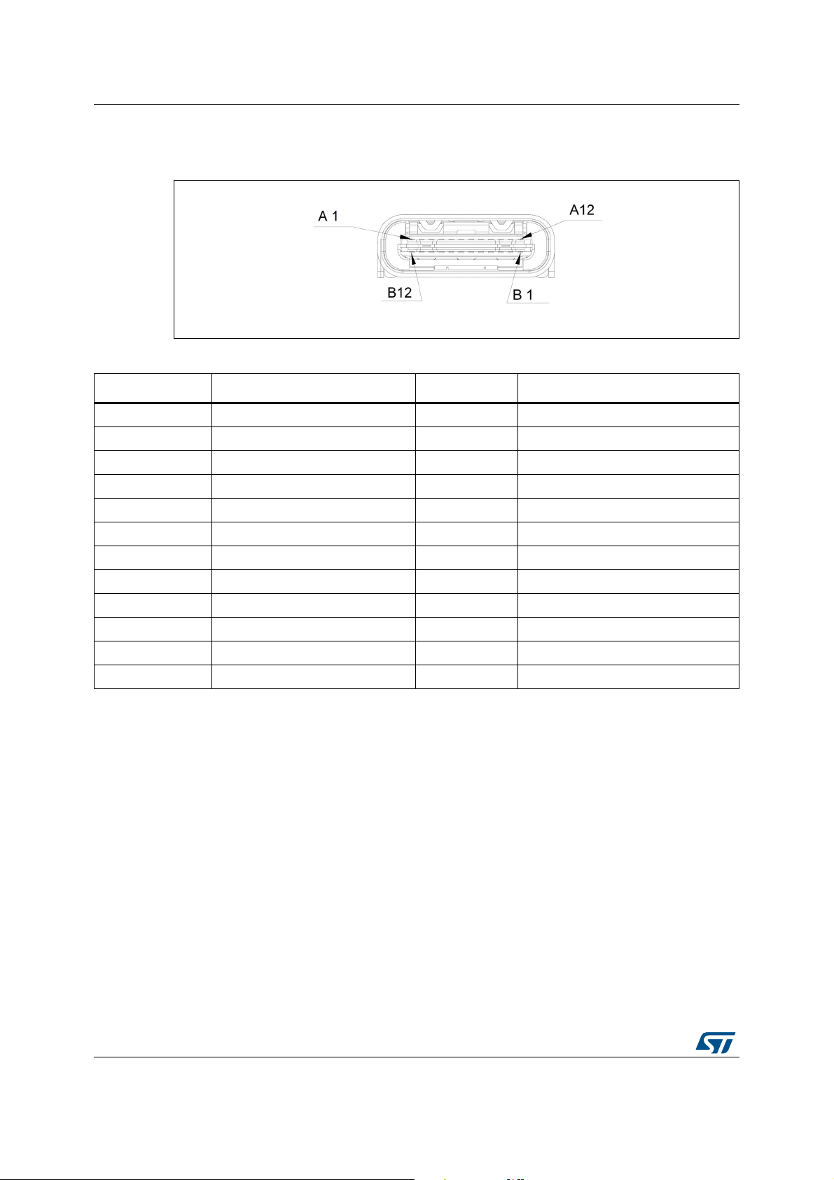
Connectors UM2403
9.3.7 USB Type-C connector PORT1 CN7
Figure 28. USB Type-C connector PORT1 CN7 (front view)
Pin number Description Pin number Description
A1 GND B1 GND
A2 TX1+ B2 TX2+
A3 TX1- B3 TX2-
A4 VBUS B4 VBUS
A5 CC1 (PA8) B5 CC2 (PB15)
A6 D+ B6 D+
A7 D- B7 D-
A8 SBU1 B8 SBU2
A9 VBUS B9 VBUS
A10 RX2- B10 RX1-
A11 RX2+ B11 RX1+
A12 GND B12 GND
Table 39. USB Type-C connector PORT1 CN7
9.3.8 Daughterboard female connector CN8 and CN9
Two female connectors CN8 and CN9 are used to implement the UCPD daughterboard on
mother board. CN8 on UCPD the daughterboard is connected to CN5 on the mother board,
and CN9 on the UCPD daughterboard is connected to CN4 on the mother board. Please
refer to
Section 9.1.3 for detail signal definition of these connectors.
46/78 UM2403 Rev 1
Page 47

UM2403 Electrical schematics
Appendix A Electrical schematics
This chapter provides design schematics for the STM32G081B-EVAL key features to help
users to implement these features in application designs:
• Figure 29: STM32G081B-EVAL mother board top on page 48
• Figure 30: STM32G081B-EVAL MCU on page 49
• Figure 31: STM32G081B-EVAL power on page 50
• Figure 32: STM32G081B-EVAL audio on page 51
• Figure 33: STM32G081B-EVAL LCD microSD on page 52
• Figure 34: STM32G081B-EVAL motor-control on page 53
• Figure 35: STM32G081B-EVAL peripherals on page 54
• Figure 36: STM32G081B-EVAL RS232 and RS485 on page 55
• Figure 37: STM32G081B-EVAL extension connectors on page 56
• Figure 38: STM32G081B-EVAL ST-LINK V2-1 on page 57
• Figure 39: STM32G081B-EVAL SWD on page 58
• Figure 40: STM32G081B-EVAL legacy peripheral daughterboard on page 59
• Figure 41: STM32G081B-EVAL legacy peripheral daughterboard HDMI and CEC on
page 60
• Figure 42: STM32G081B-EVAL legacy peripheral daughterboard Smartcard and IR on
page 61
• Figure 43: STM32G081B-EVAL legacy peripheral daughterboard temperature sensor
and LDR on page 62
• Figure 44: STM32G081B-EVAL UCPD daughterboard top on page 63
• Figure 45: STM32G081B-EVAL UCPD daughterboard CC and VCONN on page 64
• Figure 46: STM32G081B-EVAL UCPD daughterboard port1 DP USB3 on page 65
• Figure 47: STM32G081B-EVAL UCPD daughterboard Type-C source con on page 66
• Figure 48: STM32G081B-EVAL UCPD daughterboard port2 DP on page 67Figure 49:
STM32G081B-EVAL UCPD daughterboard Type-C sink con on page 68
• Figure 49: STM32G081B-EVAL UCPD daughterboard Type-C sink con on page 68
• Figure 50: STM32G081B-EVAL UCPD daughterboard USB PD on page 69
• Figure 51: STM32G081B-EVAL UCPD daughterboard power on page 70
• Figure 52: STM32G081B-EVAL UCPD daughterboard source power on page 71
UM2403 Rev 1 47/78
77
Page 48

48/78 UM2403 Rev 1
212
MB1350_TOP
Title:
Size:
Reference:
Sheet: ofA4
Revision:
Project:
STM32G081B-EVAL Mother board
MB1350B01
31-AUG-17
Variant name is not interpreted until output
Date:
-
Variant:
C14
100nF
C12
100nF
VccA
1
A1
2
A2
3
GND4DIR
5
B2
6
B1
7
VccB
8
U1
SN74LVC2T45DCUT
+3V3
R13
100K
1Mhz clock
24Mhz clock
MicroSD_CS_3V3
LCD_CS_3V3
SDcard_detect
RESET#
SPI1_MISO_3V3
SPI1_MOSI
SPI1_MOSI_DIR
SPI1_SCK
U_LCD_MicroSD
LCD_MicroSD.SchDoc
USART1_RX_3V3
Bootloader_BOOT0_3V3
Bootloader_RESET_3V3
USART1_CTS_3V3
USART1_RX_BOOT_3V3
USART1_RTS
USART1_TX
USART1_TX_BOOT
U_RS232_RS485
RS232_RS485.SchDoc
STLK_RX
STLK_TX
TMS/SWDIO
TCK/SWCLK
T_SWDIO_IN
RESET#
U_ST_LINK_V2-1
ST_LINK_V2-1.SCHDOC
RESET#
SWDAT
SWCLK
U_SWD
SWD.SchDoc
Potentiometer
LED4
LED3
LED1
LED2
Tamper_key
JOY_SEL
JOY_DOWN
JOY_LEFT
JOY_RIGHT
JOY_UP
EX_RESET
I2C1_SCL
I2C1_SDA
U_Peripherals
Peripherals.SchDoc
RESET#
LED4
LED3
LED1
LED2
Bootloader_BOOT0
Bootloader_RESET
JOY_SEL
MC_BusVoltage
MC_CurrentA
Audio_OUT_L
Audio_OUT_R
SPI1_SCK
Potentiometer
SWCLK
USART1_TX_BOOT
MC_EnA
USART1_RX_BOOT
Audio_IN
SPI1_MOSI_DIR
MC_EnB
I2C1_SCL
I2C1_SDA
MC_EnIndex
MC_DissipativeBrake
MC_EmergencySTOP
SDcard_detect
MC_PFCsync1
LCD_CS_OD
MicroSD_CS_OD
JOY_UP
JOY_DOWN
MC_HeatsinkTemperature
MC_CurrentC
MC_CurrentB
MC_PFCsync2
MC_PFCpwm
Tamper_key
USART1_CTS
USART1_RTS
USART1_TX
USART1_RX
EX_RESET_OD
JOY_LEFT
JOY_RIGHT
MC_NTC
MC_UH
MC_UL
MC_WL
MC_VH
MC_VL
MC_WH
SPI1_MISO
SPI1_MOSI
SWDAT
VREF+
PA[0..15]
PB[0..15]
PC[0..15]
PD[0..6]
PF[0..4]
PD[8..9]
VCP_TX
VCP_RX
U_MCU
MCU.SchDoc
VDD
VDD
U_Power
Power.SchDoc
MC_EmergencySTOP
MC_CurrentA
MC_CurrentB
MC_CurrentC
MC_PFCsync1
MC_PFCsync2
MC_WL
MC_VH
MC_VL
MC_UH
MC_UL
MC_WH
MC_NTC
MC_DissipativeBrake
MC_PFCpwm
MC_EnA
MC_EnB
MC_HeatsinkTemperature
MC_BusVoltage
MC_EnIndex
U_Motor Control
Motor Control.SchDoc
SB5
SB4
PA[0..15]
PB[0..15]
PC[0..15]
PD[0..6]
PF[0..4]
PD[8..9]
RESET#
U_Extension connectors
Extension connectors.SchDoc
Audio_IN
Audio_OUT_L
Audio_OUT_R
U_Audio
Audio.SchDoc
Figure 29. STM32G081B-EVAL mother board top
Electrical schematics UM2403
Page 49

Figure 30. STM32G081B-EVAL MCU
312
MCU
Title:
Size:
Reference:
Sheet: ofA4
Revision:
Project:
STM32G081B-EVAL Mother board
MB1350B01
31-AUG-17
Variant name is not interpreted until output
Date:
-
Variant:
1
43
2
B1
TD-0341 [RESET/Black]
C88
100nF
PB5
PB6
PB7
PA4
PA5
PA6
PA7
PA11
PA12
PD0
PD1
PA9
PA10
PD3
PD4
PD5
PD6
PC10
PC11
PB14
PB15
PB10
PC12
RESET#
PB8
PC5
PA0
PB9
PC13
PD8
PD9
PC6
PC7
PC8
PC9
PA1 PC1
PC2
PC3
PD2
PB1
PB2
PA15
PB3
PB0
PC4
PA3
PA13
PA14
PB4
PC0
PA2
PA8
PC14
PC15
RESET#
LED4
LED3
LED1
LED2
Bootloader_BOOT0
Bootloader_RESET
JP12
D4
BAT60JFILM
D5
BAT60JFILM
JOY_SEL
PF2
PF4
PF0
PF1
PB11
PB12
PB13
MC_BusVoltage
MC_CurrentA
Audio_OUT_L
Audio_OUT_R
SPI1_SCK
Potentiometer
SWCLK
USART1_TX_BOOT
MC_EnA
USART1_RX_BOOT
Audio_IN
SPI1_MOSI_DIR
MC_EnB
I2C1_SCL
I2C1_SDA
MC_EnIndex
MC_DissipativeBrake
MC_EmergencySTOP
SDcard_detect
PF3
MC_PFCsync1
LCD_CS_OD
MicroSD_CS_OD
JOY_UP
JOY_DOWNMC_HeatsinkTemperature
MC_CurrentC
MC_CurrentB
MC_PFCsync2
MC_PFCpwm
Tamper_key
USART1_CTS
USART1_RTS
USART1_TX
USART1_RX
EX_RESET_OD
JOY_LEFT
JOY_RIGHT
MC_NTC
MC_UH
MC_UL
MC_WL
MC_VH
MC_VL
MC_WH
SPI1_MISO
SPI1_MOSI
SWDAT
R38 0
PF2 - NRST
12
PC0
13
PC1
14
PA6
23
PA7
24
PC4
25
PC5
26
PB2
29
PB10
30
PB11
31
PB12
32
PB15
35
PA8
36
PA9
37
PA15
47
PD3
53
PD4
54
PC11
1
PC12
2
PC13
3
PC14 - OSC32_IN
4
PC15 - OSC32_OUT
5
PF4 - VREF+
7
VDD_1
8
VSS_1
9
PC2
15
PC3
16
PA0
17
PA1
18
PB13
33
PB14
34
PC6
38
PC7
39
PD8[VSS_2]
40
PD9[VDD_2]
41
PA10
42
PA11 [PA9]
43
PA12 [PA10]
44
PA13
45
PA14 - BOOT0
46
PD5
55
PD6
56
PB3
57
PB4
58
PB5
59
PB6
60
PB7
61
PB8
62
PB9
63
PC10
64
PF0 - OSC_IN
10
PF1 - OSC_OUT
11
PA2
19
PC8
48
PD1
51
PD2
52
PA5
22
PA4
21
PF3 - VBAT
6
PD0
50
PB1
28
PA3
20
PC9
49
PB0
27
U7
STM32G0
3
2
1
JP9
X2
NX3215SA-32.768KHZ-EXS00A-MU00525
C34
4.7pF
C35
4.7pF
SB11
SB10 C36
3.9pF
C37
3.9pF
R46
0
R45
0
VDD
BT1
CR1220 holder
1
2
3
JP15
VDD
L1
BEAD(FCM1608KF-601T03)
SB22
SB17
VREF+
VDD_MCUVDD
JP11
VDD_MCU
PA[0..15]
PA[0..15]
PB[0..15]
PB[0..15]
PC[0..15]
PC[0..15]
PD[0..6]
PD[0..6]
PF[0..4]
PF[0..4]
PD[8..9]
PD[8..9]
C33
100nF
VDD_MCU
C31
4.7uF
C32
100nF
VREF+
C39
1uF
C38
10nF
VREF+
TP4
VREF+
VCP_TX
VCP_RX
DB_DET
SB23
1 2
X3
NX3225GD-8.000M-EXS00A-CG04874
R43
0
R44
0
SB14
SB13
R84 0
UM2403 Electrical schematics
UM2403 Rev 1 49/78
Page 50

412
Power
Title:
Size:
Reference:
Sheet: ofA4
Revision:
Project:
STM32G081B-EVAL Mother board
MB1350B01
31-AUG-17
Variant name is not interpreted until output
Date:
-
Variant:
SV
1
SG
2
CV
3
CG1
4
CG2
5
CG3
6
L2
BNX002-01
C70
220uF
E5V
C56
10uF[ESR<0.2ohm]
VDD_ADJ
+5V TP6
VDD_ADJ
1
3
2
CN16
DC-10B
C79
100nF
1
2
3
U18
ZEN056V130A24LS
13
2
RV2
3386P-503H[5%]
R64
11.8K[1%]
C53
[N/A]
Power Supply VDD_ADJ [1.65V to 3.5V]
R65
22.1K[1%]
C57
4.7uF
Vout=1.22*(1+R1/R2)
considering potentiometer error tolerance
C55
100nF
R79
[N/A]
VDD
JP13
VDD_ANA
3
2
1
JP16
TP5
VDD
VDD_PG
+3V3
VDD_ADJ
TP10
5V
+5V
R71
1K
1 2
LD7
green
TP11
Ground
E5V
D5V
78
56
34
12
JP17
Header 4X2
EN
1
GND
2
VO
4
ADJ
5
GND
7
VI
6
PG
3
U14
ST1L05BPUR
+5V
+5V TP7
+3V3
C72
4.7uF
C67
[N/A]
R88 20.5K[1%]
R87
11.8K[1%]
C71
10uF[ESR<0.2ohm]
EN
1
GND
2
VO
4
ADJ
5
GND
7
VI
6
PG
3
U16
ST1L05BPUR
Power Supply 3.3V
Vout=1.22*(1+R1/R2)
C64
100nF
+3V3
R91
[N/A]
+3V3_PG
+5V
R80 [N/A]+3V3_PG
C62
[N/A]
TP3
Ground
TP1
Ground
TP12
Ground
VUSB_ST_LINK
U5V_ST_LINK
12
D7
ESDA7P60-1U1M
+5V TP13
+3V3_SD
C92
4.7uF
C94
[N/A]
R116 20.5K[1%]
R117
11.8K[1%]
C95
10uF[ESR<0.2ohm]
EN
1
GND
2
VO
4
ADJ
5
GND
7
VI
6
PG
3
U21
ST1L05BPUR
Power Supply 3.3V
Vout=1.22*(1+R1/R2)
C96
100nF
+3V3_SD
R114
[N/A]
+3V3_SD_PG
+5V
R115 0+3V3_PG
C93
[N/A]
+3V3
SB46
SB47
+3V3_SD
50/78 UM2403 Rev 1
Figure 31. STM32G081B-EVAL power
Electrical schematics UM2403
Page 51

UM2403 Rev 1 51/78
512
Audio
Title:
Size:
Reference:
Sheet: ofA4
Revision:
Project:
STM32G081B-EVAL Mother board
MB1350B01
31-AUG-17
Variant name is not interpreted until output
Date:
-
Variant:
C47
180pF
C51
100nF
R66
100K
R69
100K
TP9
MIC_OUT
TP8
MIC+
R74
1K
R72
100
R73
2.2K
C54
47pF
R67
15K
13
2
RV1
[N/A]
C46
[N/A]
R62 0
R61
510
Audio_IN
4
3
1
2 5
U12
TS461CLT
C61
10uF
C59
4.7uF
C60
2.2uF
R68
18K
R59 82K
R70
680
C58
4.7uF
PA6
VDD_ANA
VDD_ANA
VDD_ANA
C50
100nF
R108
10K
JP18
C69
1uF
C66
330nF
R89
20K
Audio_OUT_L
C65
[N/A]
C80
330nF
R95
20K
Audio_OUT_R
R93
0
C78
[N/A]
R90
4.7K
C73
1.5nF
R94
4.7K
C76
1.5nF
C68
220uF
R86
1K
C77
220uF
R92
1K
C75
1uF
Default setting: close
C74
100nF
VDD_ANA
VDD_ANA
VDD_ANA>2.2V
VDD_ANA>2.7V
PA4
PA5
3
2
1
JP6
Shutdown
6
Bypass
4
VIN2
7
VIN1
3
VOUT1
2
VCC
1
GND
5
VOUT2
8
9
U17
TS488IQT
JP4
2
6
4
3
CN15
PJ3028B-3
Left
Right
Microphone
13245
6
D6
ESDA6V1BC6
JP19
Figure 32. STM32G081B-EVAL audio
UM2403 Electrical schematics
Page 52

52/78 UM2403 Rev 1
612
LCD_MicroSD
Title:
Size:
Reference:
Sheet: ofA4
Revision:
Project:
STM32G081B-EVAL Mother board
MB1350B01
31-AUG-17
Variant name is not interpreted until output
Date:
-
Variant:
MicroSD_CS_3V3
LCD_CS_3V3
SDcard_detect
CS
1
SCL
2
SDI
3
RS
4
WR
5
RD
6
RESET
8
VDD
9
VCI
10
SDO
7
GND
11
GND
12
BL_VDD
13
BL_Control
14
BL_GND
15
BL_GND
16
CN14
2.4" LCD connector (MB895C)
TFT LCD
PC9
+5V
C82
10uF
L3
BEAD
C81
100nF
L4
BEAD
R96 0
R100 [N/A]
R60
10K
R34
10K
RVS
1
CS
2
DI
3
Vdd
4
SCLK
5
Vss
6
DO
7
RVS
8
SW2
9
SW1
10
CN8
PJS008-2000 (SMS064FF or SMS128FF)
PB8
PD1
RESET#
VDD
R75
4.7K
R76 270
R78
10K
R63
270
Open drain pin!
Open drain pin!
SPI LCD
SPI MICRO SD
SPI1_MISO_3V3
PB4
SPI1_MOSI
PA7
VCCA
1
A1
2
A2
3
GND4DIR
5
B2
6
B1
7
VCCB
8
U10
SN74LVC2T45DCUT
VDD
VDD
C40
100nF
C42
100nF
SPI1_MOSI_3V3
SPI1_MOSI_DIR
R56 10K
PC12
SPI1_SCK
VCCA
1
A1
2
A2
3
GND4DIR
5
B2
6
B1
7
VCCB
8
U11
SN74LVC2T45DCUT
VDD
VDD
C43
100nF
C41
100nF
SPI1_SCK_3V3
PB3
R57
100K
VDD
SPI1_MOSI_3V3
SPI1_SCK_3V3
WP/CD
1
RDAT3_GND
2
DAT2_IN
3
DAT3_IN
4
CMD_IN
5
CLK_IN
6
DAT0_IN
7
DAT1_IN
8
DAT1_EX
9
DAT0_EX
10
CLK_EX
11
CMD_EX
12
DAT3_EX
13
DAT2_EX
14
VCC
15
RDATA_VCC
16
GND
17
U6
EMIF06-MSD02N16
SB8
SB12
SB9
SB27
SB24
SB26
SB25
SB15
1
2 3
G
SD
T2
BSN20
+3V3_SD
+3V3_SD
+3V3_SD
+3V3_SD
+3V3_SD
+3V3_SD
+3V3_SD
+3V3_SD
+3V3_SD
Figure 33. STM32G081B-EVAL LCD microSD
Electrical schematics UM2403
Page 53

712
Motor Control
Title:
Size:
Reference:
Sheet: ofA4
Revision:
Project:
STM32G081B-EVAL Mother board
MB1350B01
31-AUG-17
Variant name is not interpreted until output
Date:
-
Variant:
C5
1nF
+3V3
+5V
R2
0
C10
100nF
C6
100nF
R6 0
C9
[N/A]
C8
[N/A]
C7
[N/A]
C4
[N/A]
C11
10nF
C2
[N/A]
C3
[N/A]
R5 0
R4 0
R7
0
R3
0
EMERGENCY STOP
1
MC-UH
3
MC_UL
5
MC_VH
7
MC_VL
9
MC_WH
11
MC_WL
13
CURRENT A
15
CURRENT C
19
CURRENT B
17
NTC BYPASS RELAY
21
DISSIPATIVE BRAKE
23
+5V POWER
25
PFC SYNC
27
PFC PWM
29
Encoder A
31
Encoder B
33
GND
2
GND
4
GND
6
GND
8
GND
10
GND
12
BUS VOLTAGE
14
GND
16
GND
18
GND
20
GND
22
GND
24
Heatsink Temperature
26
3.3V Power
28
GND
30
GND
32
Encoder Index
34
CN1
MC_connector
MC_EmergencySTOP
MC_CurrentA
MC_CurrentB
MC_CurrentC
MC_PFCsync1
MC_PFCsync2
MC_WL
MC_VH
MC_VL
MC_UH
MC_UL
MC_WH
MC_NTC
MC_DissipativeBrake
MC_PFCpwm
MC_EnA
MC_EnB
MC_HeatsinkTemperature
MC_BusVoltage
MC_EnIndex
R8
100K
C1
[N/A]
Motor control connector
Default setting: Open
PB12
PA8
PD2
PA9
PD3
PA10
PD4
PB15
PB5
PB10
PA1
PC1
PB1
PA6
PD0
PA2
PA3
R1
3.3K
+3V3
SB1
SB2
JP1
JP2
Default setting: Open
Default setting: Open
JP3
PB9
PB0
PC6
UM2403 Rev 1 53/78
Figure 34. STM32G081B-EVAL motor-control
UM2403 Electrical schematics
Page 54

812
Peripherals
Title:
Size:
Reference:
Sheet: ofA4
Revision:
Project:
STM32G081B-EVAL Mother board
MB1350B01
31-AUG-17
Variant name is not interpreted until output
Date:
-
Variant:
13
2
RV3
10K
Potentiometer
Potentiometer
1 2
LD3
Red
1 2
LD2
Orange
1 2
LD4
Blue
1 2
LD1
Green
+3V3
R104
510
R103
680
R102
680
R101
680
LED4
LED3
LED1
LED2
LEDs
Tamper Button
PD5
PD6
PD8
PD9
C90
[N/A]
R1110
Close to MCU on PCB
PB2
R1130
CN17
two pin header for external analog input
R109
4.7K
1
4 3
2
B2
Tamper
C89
100nF
VDD
R110
100
Tamper_key
PC13
R11247
VDD_ANA
C91
100nF
VDD
C87 100nF
C86 100nF
C85 100nF
C83 100nF
C84 100nF
R106
100
COMMON
5
Selection
2
DOWN
3
LEFT
1
RIGHT
4
UP
6
GND
7
GND
8
B3
MT-008A
JOY_SEL
JOY_DOWN
JOY_LEFT
JOY_RIGHT
JOY_UP
Joystick
PC2
PC7
PC8
PC3
PA0
Input pins with pull-down
VDD
+3V3
R99
1K[1%]
R97
4.53K[1%]
+3V3
+3V3
6
5
7
U19B
TS3702IPT
2
3
1
4 8
U19A
TS3702IPT
12
LD8
Orange
VDD<2.7V
R105 0
R98
0
R83
510
Low Voltage LED
IOs and some Analog IPs will work with degraded performances
EX_RESET
PC0
R12
10K
EXT_I2C_PWR
Open drain pin!
1 2
3 4
5 6
7 8
CN2
F206A-2*04MGF-A
SSM-104-L-DH (Samtec)
I2C1_SCL
I2C1_SDA
R10
10K
I2C_PU
R9
10K
I2C extension connector
VDD
R107 0D9
ESDALC6V1-1U2
PB7
PB6
SB43
SB36
SB35
SB34
SB33
SB42
SB38
SB37
SB39
SB40
SB41
EXT_I2C_PWR
1
3
2 4
5
6
D8
ESDA6V1-5SC6
54/78 UM2403 Rev 1
Figure 35. STM32G081B-EVAL peripherals
Electrical schematics UM2403
Page 55

912
RS232_RS485
Title:
Size:
Reference:
Sheet: ofA4
Revision:
Project:
STM32G081B-EVAL Mother board
MB1350B01
31-AUG-17
Variant name is not interpreted until output
Date:
-
Variant:
1
6
2
7
3
8
4
9
5
CN11
DB9-male USART1
USART1_RX_3V3
connector for USART1 & RS485
R81
10K
R77
22K
R85
22K
R82
120
C63
100nF
Bootloader_BOOT0_3V3
Bootloader_RESET_3V3
C2+
1
C2-
2
V-
3
R1IN
4
R2IN
5
R3IN
6
R4IN
7
R5IN
8
T1OUT
9
T2OUT
10
T3OUT
11
T3IN
12
T2IN
13
T1IN
14
R5OUT
15
R4OUT
16
R3OUT
17
R2OUT
18
R1OUT
19
R2OUTB
20
R1OUTB
21
nSHDN
22
nEN
23
C1-
24
GND
25
VCC
26
V+
27
C1+
28
U13
ST3241EBPR
C49
100nF
C45
100nF
C52
100nF
C48
100nF
C44
100nF
+3V3
+3V3
RXD
RTS
TXD
CTS
DSR
USART1_CTS_3V3
PA11
RO
1
RE
2
DE
3
DI4GND
5
A
6
B
7
Vcc
8
U15
ST3485EBDR
+3V3
PA10
3
2
1
JP10
3
2
1
JP8
USART1_RX_BOOT_3V3
PC5
USART1_RTS_3V3
USART1_RTS
PA12
VCCA
1
A1
2
A2
3
GND4DIR
5
B2
6
B1
7
VCCB
8
U8
SN74LVC2T45DCUT
+3V3VDD
VDD
C29
100nF
C30
100nF
R40
100K
R42
100K
VDD
USART1_TX
PC4
PA9
USART1_TX_BOOT
USART1_TX_3V3
USART1_TX_3V3
USART1_RTS_3V3
RS485_DIR
RS485_DIR
3
2
1
JP14
SB28
SB16
SB29
SB31
SB32
SB30
USART1_RTS_3V3
UM2403 Rev 1 55/78
Figure 36. STM32G081B-EVAL RS232 and RS485
UM2403 Electrical schematics
Page 56

56/78 UM2403 Rev 1
10 12
Extension connectors
Title:
Size:
Reference:
Sheet: ofA4
Revision:
Project:
STM32G081B-EVAL Mother board
MB1350B01
31-AUG-17
Variant name is not interpreted until output
Date:
-
Variant:
PA4
PA5 PA6
PA7
PA11
PA12
PA0
PA1
PA15
PA3
PA13
PA14
PB6
PB7
PB14
PB10
PB8
PB1
PB2
PB4
PB11
PB12
PB13
PB3
PC10 PC11 PC12
PC5
PC13
PC6
PC7
PC8
PC9
PC2
PC3PC4
PC0
PC14
PC15
PD1
PD5
PD6
PD8 PD9
PF2
PF4
PF0
PF1
PF3
PA[0..15]
PA[0..15]
PB[0..15]
PB[0..15]
PC[0..15]
PC[0..15]
PD[0..6]
PD[0..6]
PF[0..4]
PF[0..4]
PD[8..9]
PD[8..9]
SOURCE_EN
DISCHARGE_1
DISCHARGE_2
VSENSE_1
ISENSE_1
DB_DET DB_DET
+3V3
HPDIN
USB3_DET
I2C1_SCL
I2C1_SDA
RESET(Mother board)
ISENSE_2
VSENSE_2
VDD
I2C_PU
USB-C daugher board signal Legacy daugher board signal
IR_IN
I2C2_SCL
I2C2_SDA
HDMI_CEC
LDR_OUT
SMART_RST
RESET(Mother board)
SMART_OFF
SMART_1V8
I2C1_SCL
I2C1_SDA
R11 820
R26 10K
RESET#
D5V
VDD
SB20
SB21
+3V3
R47 820
SB18
SB19
Daugher board connectors
Extension connectors
VDD_ANA
R41 820
1
2
3
4
5
6
7
8
9
10
11
12
13
14
15
16
17
18
CN4
Header 18X1
R39 10K
BOOT0
1 2
3 4
5 6
7 8
9 10
11 12
13 14
15 16
17 18
19 20
21 22
CN10
Header 11X2
1 2
3 4
5 6
7 8
9 10
11 12
13 14
15 16
17 18
19 20
21 22
CN9
Header 11X2
PA9
PA10
PA2
PA8
PB5
PB15
PB9
PB0
PC1
PD0
PD3
PD4
PD2
PORT1_CC1
PORT1_DB1
VCONN_EN1
VCONN_EN2
FRS_TX1
V_CTRL2
V_CTRL1
PORT1_CC2
PORT1_DB2
FRS_TX2
USB-C daugher board signalLegacy daugher board signal
PORT2_CC1
PORT2_CC2
HPD_SOURCE
D5V
VDD
SMART_CK
IR_OUT
SMART_TX
TEMP_SENSOR_INT
SMART_3/5V
SMART_CMDVCC
HDMI_HPD_SINK
HDMI_HPD_SOURCE
+5V
1
2
3
4
5
6
7
8
9
10
11
12
13
14
15
16
17
18
CN5
Header 18X1
EXT_I2C_PWR
SB44
SB45
Note: If no daugher board on CN4 & CN5, close pin17 &18 of CN4 & CN5 by jumpers when using I2C extension connector CN2
Figure 37. STM32G081B-EVAL extension connectors
Electrical schematics UM2403
Page 57

11 12
ST_LINK_V2-1
Title:
Size:
Reference:
Sheet: ofA4
Revision:
Project:
STM32G081B-EVAL Mother board
MB1350B01
31-AUG-17
Variant name is not interpreted until output
Date:
-
Variant:
STM_RST
T_JTCK
T_JTCK
T_JTDO
T_JTDI
T_JTMS
OSC_IN
OSC_OUT
T_NRST
AIN_1
COM
PWR
Board Ident: PC13=0
SWD
T_SWDIO_IN
LED_STLINK
MCO
CN3
[N/A]
TX
RX
STLINK_RX
STLK_RX
STLK_TX
STLINK_TX
T_SWO
R25
[N/A]
R17
100K
R24
10K
R14 4.7K
R15 4.7K
C16
100nF
D5V
USB_RENUMn
+3V3_ST_LINK
+3V3_ST_LINK
+3V3_ST_LINK
+3V3_ST_LINK
PWR_EXT
+3V3_ST_LINK
C26
1uF_X5R_0603
C24
10nF_X7R_0603
C23
1uF_X5R_0603
C27
100nF
C22
100nF
+3V3_ST_LINK
VBAT
1
PA7
17
PC13
2
PA12
33
PC14
3
PB0
18
PC15
4
JTMS/SWDIO
34
OSCIN
5
PB1
19
OSCOUT
6
VSS_2
35
NRST
7
PB2/BOOT1
20
VSSA
8
VDD_2
36
VDDA
9
PB10
21
PA0
10
JTCK/SWCLK
37
PA1
11
PB11
22
PA2
12
PA15/JTDI
38
PA3
13
VSS_1
23
PA4
14
PB3/JTDO
39
PA5
15
VDD_1
24
PA6
16
PB4/JNTRST
40
PB12
25
PB5
41
PB13
26
PB6
42
PB14
27
PB7
43
PB15
28
BOOT0
44
PA8
29
PB8
45
PA9
30
PB9
46
PA10
31
VSS_3
47
PA11
32
VDD_3
48
U2
STM32F103CBT6
R16
100K
PWR_ENn
+3V3_ST_LINK
1 2
3 4
5
CN7
[N/A]
C20
100nF
C13
100nF
C15
100nF
C21
100nF
+3V3_ST_LINK
VUSB_ST_LINK
LED_STLINK
21
4 3
Red Yellow
LD6
HSMF-A201-A00J1
R35
100
R36
100
R37
0
+3V3_ST_LINK
T_JTCK
T_NRST
T_JTMS
TMS/SWDIO
TCK/SWCLK
T_SWDIO_IN
RESET#
T_SWDIO_IN
STM_JTMS_SWDIO
STM_JTCK_SWCLK
STM_JTMS_SWDIO
STM_JTCK_SWCLK
D2
BAT60JFILM
D3
BAT60JFILM
T_JRST
SWIM_PU_CTRL
STL_USB_DM
STL_USB_DP
R23
100K
R28
2.7K
R27
4.7K
+3V3_ST_LINK
+5V
PC11
PC10
C28
4.7uF
VUSB_ST_LINK U5V_ST_LINK
R31 100K
C25
100nF
D1
BAT60JFILM
JP5
1 2
LD5
Red
R33
1K
USB ST-LINK
R18
1.5K
R19
100K
USB_RENUMn
R21
10K
R20
36K
R22 100
+3V3_ST_LINK
I/O1
1
GND
2
I/O23I/O2
4
Vbus
5
I/O1
6
U3
USBLC6-2SC6
C17
100nF
i
Diff Pair 90ohm
i
Diff Pair 90ohm
VBUS
1
DM
2
DP
3
ID
4
GND
5
Shield
6
USB_Micro-B receptacle
Shield
7
Shield
8
Shield
9
EXP
10
EXP
11
CN6
1050170001
3
1
2
T1
9013
VUSB_ST_LINK
VUSB_ST_LINK
VUSB_ST_LINK
STL_USB_DM
STL_USB_DP
51
2
GND
3
4
BYPASS
EN
Vin Vout
U4 LDK120M33R
C19
10pF
C18
10pF
1 2
X1
NX3225GD-8.000M-EXS00A-CG04874
VDD
SB6
SB7
TP2
PB10
PA14
PA13
PA13
SB3
JP7
R32
10K
D10
BAT60JFILM
E5V
GND
2
IN
5
EN
4
OUT
1
FAULT
3
STMPS2141STR
U5
U4 can be replaced by LD3985M33R
UM2403 Rev 1 57/78
Figure 38. STM32G081B-EVAL ST-LINK V2-1
Power Switch to supply +5V
from STLINK USB
UM2403 Electrical schematics
Page 58

58/78 UM2403 Rev 1
12 12
SWD
Title:
Size:
Reference:
Sheet: ofA4
Revision:
Project:
STM32G081B-EVAL Mother board
MB1350B01
31-AUG-17
Variant name is not interpreted until output
Date:
-
Variant:
R49
[N/A]
R51
[N/A]
R53
[N/A]
1
2
3
4
5
6
7
8
9
10
11
12
13
14
15
16
17
18
19
20
CN12
SWD
R55 10K
R58 10K
R52
10K
RESET#
SWDAT
SWCLK
High Density SWD connector
Standard SWD connector
KEY
PA13
PA14
R48 22
R50 22
R54 22
1
2
3
4
5
6
7
8
9
10
CN13
FTSH-105-01-L-DV
VDD
VDD
VDD
1
324
5
U9
ESDALC6V1W5
VDD
Figure 39. STM32G081B-EVAL SWD
Electrical schematics UM2403
Page 59

Figure 40. STM32G081B-EVAL legacy peripheral daughterboard
25
MB1351_TOP
Title:
Size:
Reference:
Sheet: ofA4
Revision:
Project:
STM32G081B-EVAL Legacy peripheral daughter board
MB1351A01
17-MAY-17
Variant name is not interpreted until output
Date:
-
Variant:
DB_DET
Legacy daugher board signal
+3V3
VDD VDD
PD4
PB9
PA2
PB5
PC6
PB13
PB14
PB10
PB15
PB0
LDR_OUT
SMART_RST
HDMI_HPD_SINK
RESET(Mother board)
SMART_OFF
SMART_1V8
I2C1_SCL
I2C1_SDA
HDMI_HPD_SOURCE
R21 20K
VDD_ANA
HDMI_HPD_SINK
I2C2_SDA_5V
I2C2_SCL_5V
HDMI_CEC_3V3
HDMI_HPD_Source_5V
I2C1_SCL_5V
I2C1_SDA_5V
U_HDMI_CEC
HDMI_CEC.SchDoc
SmartCard_3/5V
SmartCard_IO
SmartCard_RST
SmartCard_CLK
SmartCard_OFF
SmartCard_CMDVCC
IR_OUT
IR_IN
SmartCard_1V8
U_SmartCard_IR
SmartCard_IR.SchDoc
I2C1_SCL_5V
I2C1_SDA_5V
TempSensor_INT
LDR_OUT
U_TemSensor_LDR
TemSensor_LDR.SCHDOC
SmartCard_3/5V
SmartCard_CLK
SmartCard_IO
SmartCard_CMDVCC
SmartCard_1V8
SmartCard_RST
SmartCard_OFF
IR_IN
IR_OUT
I2C1_SCL_5V
I2C1_SDA_5V
TempSensor_INT
LDR_OUT
HDMI_HPD_Source_5V
HDMI_HPD_SINK
HDMI_CEC_3V3
I2C1_SCL_5V
I2C1_SDA_5V
I2C2_SCL_5V
I2C2_SDA_5V
SMART_CK
IR_OUT
SMART_TX
IR_IN
I2C2_SCL
I2C2_SDA
HDMI_CEC
SMART_3/5V
SMART_CMDVCC
PA1
PA15
PD2
PB12
PA3
PB6
PB7
PD3
SmartCard_3/5V
SmartCard_CLK
SmartCard_IO
SmartCard_CMDVCC
SmartCard_1V8
SmartCard_RST
SmartCard_OFF
IR_IN IR_OUT
I2C1_SCL_5V
I2C1_SDA_5V
TempSensor_INT
LDR_OUT
HDMI_HPD_Source_5V
HDMI_HPD_SINK
HDMI_CEC_3V3
I2C2_SCL_5V
I2C2_SDA_5V
SB8
+5V
RST_PU_POWER
+5V
+3V3
1
2
3
4
5
6
7
8
9
10
11
12
13
14
15
16
17
18
CN4
Header 18X1_Female
1
2
3
4
5
6
7
8
9
10
11
12
13
14
15
16
17
18
CN5
Header 18X1_Female
C13
100nF
C14
100nF
VDD
C8
100nF
+3V3
C4
100nF
+5V VDD_ANA
C10
100nF
UM2403 Electrical schematics
UM2403 Rev 1 59/78
Page 60

60/78 UM2403 Rev 1
35
HDMI_CEC
Title:
Size:
Reference:
Sheet: ofA4
Revision:
Project:
STM32G081B-EVAL Legacy peripheral daughter board
MB1351A01
17-MAY-17
Variant name is not interpreted until output
Date:
-
Variant:
HDMI_HPD_SINK
Sink
Source
R20
1K
R7
1K
HDMI_5V_Sink
HDMI_5V_Sink
I2C2_SDA_5V
I2C2_SCL_5V
R9
47K
R10
47K
+3V3
R18
27K
HDMI_CEC_3V3
+5V
C2
4.7uF
GND
2
IN
5
EN
4
OUT
1
FAULT
3
U1
STMPS2141STR@54
HDMI_5V_Source
R22
1M
HDMI_HPD_Source_5V
I2C1_SCL_5V
I2C1_SDA_5V
R4
1.8KR31.8K
+5V
R15
0
+5V
PD2
PB13
PB14
PB10
PD3
PB6
PB7
TMDS_Data2+
TMDS_Data2TMDS_Data1+
TMDS_Data1TMDS_Data0+
TMDS_Data0TMDS_Clock+
TMDS_Clock-
R8
1K
FT pin & Open Drain mode needed
Open drain pin!
1
2
3
4
5
6
7
8
9
10
11
12
13
14
15
16
17
18
19
22
20
21
CN3
HD119F-3A09200
1
2
3
4
5
6
7
8
9
10
11
12
13
14
15
16
17
18
19
22
20
21
CN1
HD119F-3A09200
SB3
SB4
SB5
SB6
3
1
2
T1
9012
2
1
3
G
SD
T4
2N7002
Figure 41. STM32G081B-EVAL legacy peripheral daughterboard HDMI and CEC
Electrical schematics UM2403
Page 61

Figure 42. STM32G081B-EVAL legacy peripheral daughterboard Smartcard and IR
45
SmartCard_IR
Title:
Size:
Reference:
Sheet: ofA4
Revision:
Project:
STM32G081B-EVAL Legacy peripheral daughter board
MB1351A01
17-MAY-17
Variant name is not interpreted until output
Date:
-
Variant:
VCC
1
RST
2
CLK
3
NC
4
GND
5
NC
6
I/O
7
NC
8
18
17CN2
C816
C9 100nF
C6
100nF
C3
47uF
+5V
C5 100nF
C12
100nF
R16
100K
R17
4.7K
R25
10K[N/A]
R24
10K[N/A]
C11
100nF
C15
47uF
R27
10K
R26
10K
TP2
AUX2
TP1
AUX1
SmartCard_3/5V
SmartCard_IO
SmartCard_RST
SmartCard_CLK
SmartCard_OFF
SmartCard_CMDVCC
PA15
PB12
PD4
PA2
PB0
PB15
IR_OUT
R6
22
+3V3
R5
100
12
LD1
SFH409-2
IR_LED
PB9
VDD
R12
10K
R13
1K
+3V3
2
3
1
D1
TSOP34836
R14
100
C1
4.7uF
IR_IN
PC6
IR
VDD>2.7V
IR_Receiver
CLKDIV1
1
CLKDIV2
2
5V/3V
3
PGND
4
C1+
5
Vddp
6
C1-
7
Vup
8
PRES
9
PRES
10
I/O
11
AUX2
12
AUX1
13
CGND14CLK
15
RST
16
Vcc
17
PORADJ/1.8V
18
CMDVCC
19
RSTIN
20
Vdd
21
GND
22
OFF
23
XTAL1
24
XTAL2
25
I/OUC
26
AUX1UC
27
AUX2UC
28
U2
ST8024LACDR
SmartCard_1V8
PA3
R11
10K
VDD
VDD
VDD
VDD
VDD
Smart Card
SB2
SB1
3
1
2
T3
9013
3
1
2
T2
9013
UM2403 Electrical schematics
UM2403 Rev 1 61/78
Page 62

62/78 UM2403 Rev 1
55
TemSensor_LDR
Title:
Size:
Reference:
Sheet: ofA4
Revision:
Project:
STM32G081B-EVAL Legacy peripheral daughter board
MB1351A01
17-MAY-17
Variant name is not interpreted until output
Date:
-
Variant:
SDA
1
SCL
2
OS/INT
3
GND4A2
5
A1
6
A0
7
VDD
8
U3
STLM75M2F
+5V
C7
100nF
R23
10K
VDD
I2C1_SCL_5V
I2C1_SDA_5V
Temperature sensor
TempSensor_INT
PB7
PB6
PB5
R19
10K
+5V
Address:100100(A0)
LDR_OUT
R2
8.2K
PA1
R1
VT9ON1
Photo resistor
VDD_ANA
SB7
Figure 43. STM32G081B-EVAL legacy peripheral daughterboard temperature sensor and LDR
Electrical schematics UM2403
Page 63

210
MB1352_TOP
Title:
Size:
Reference:
Sheet: ofA4
Revision:
Project:
STM32G081B-EVAL USB-C daughter board
MB1352C02
3-Aug-18
Variant name is not interpreted until output
Date:
-
Variant:
Mother board connectors
R107
10K
R106
10K
R120 15K[1%]
+3V3
VDD
PA8
PA9
PB15
D5V
VDD
+5V
PA10
PD4
PB9
PA2
PB0
PB5
PC1
PC6
PB13
PB14
PB1
PB10
SB59
VDD
DB_DET
+3V3
RESET
VDD
PA1
PA15
PB6
PB7
PD0
PD2
PD3
PA3
PB12
PORT1_CC1
PORT1_CC1
PORT1_CC2
PORT1_CC2
PORT1_DB1
PORT1_DB1
PORT1_DB2
VCONN_EN1
VCONN_EN2
FRS_TX1
FRS_TX2
PORT1_DB2
VCONN_EN1
VCONN_EN2
FRS_TX1
FRS_TX2
SOURCE_EN
DISCHARGE_1
DISCHARGE_2
VSENSE_1
ISENSE_1
SOURCE_EN
DISCHARGE_1
DISCHARGE_2
VSENSE_1
ISENSE_1
HPDIN
USB3_DET
I2C_SCL
I2C_SDA
HPDIN
USB3_DET
I2C_SCL
I2C_SDA
RESET#
PORT2_CC1
PORT2_CC2
HPD_SOURCE
VSENSE_2
ISENSE_2
VSENSE_2
ISENSE_2
HPD_SOURCE
RESET#
PORT2_CC1
PORT2_CC2
U_POWER
POWER.SchDoc
SOURCE_EN
VSENSE_1
DISCHARGE_1
ISENSE_1
VSENSE_2
ISENSE_2
DISCHARGE_2
U_USB_PD
USB_PD.SchDoc
1
2
3
4
5
6
7
8
9
10
11
12
13
14
15
16
17
18
CN9
Header 18X1_Female
1
2
3
4
5
6
7
8
9
10
11
12
13
14
15
16
17
18
CN8
Header 18X1_Female
C101
100nF
C102
100nF
VDD
C100
100nF
+3V3
C97
100nF
+5V
PORT1_CC1
PORT1_CC2
VCONN_EN1
VCONN_EN2
FRS_TX1
FRS_TX2
CON1_CC1
CON1_CC2
PORT1_DB1
PORT1_DB2
U_CC & VCONN
CC & VCONN.SchDoc
1
2
3
4
CN10
Header 4X1_Female
CON1_D+
CON1_DCON2_D+
CON2_D-
RFU
I2C_SCL
I2C_SDA
HPDIN
USB3_DET
1_CC1
1_CC2
CON1_D-
CON1_D+
U_PORT1_DP_USB3
PORT1_DP_USB3.SchDoc
I2C_SCL
I2C_SDA
HPD_SOURCE
RESET#
PORT2_CC1
PORT2_CC2
CON2_D-
CON2_D+
U_PORT2_DP
PORT2_DP.SchDoc
CON1_D+
CON1_D-
CON2_D+
CON2_D-
1
3 2
4 5
6
D10
ESDA5V3SC6
PORT1_CC1
PORT1_CC2
PORT2_CC1
PORT2_CC2
V_CTL1
V_CTL2
V_CTL1
V_CTL2
V_CTL2
V_CTL1
VSENSE_DCDC
DCDC_EN
U_SOURCE POWER
SOURCE POWER.SchDoc
DCDC_EN
VSENSE_DCDC
VCC
2
GND
5
S1
4
D
1
SEL
3
S2
6
U7
STG5123
+3V3
C38 100nF
DCDC_EN
R82
[N/A]
VSENSE_DCDC
ADC input PB11
DCDC_EN=0: Daugher board detection:1.32V
DCDC_EN=1: U18 output measurement:0.43V-3.3V
SB24
UM2403 Rev 1 63/78
Figure 44. STM32G081B-EVAL UCPD daughterboard top
UM2403 Electrical schematics
Page 64

64/78 UM2403 Rev 1
310
CC & VCONN
Title:
Size:
Reference:
Sheet: ofA4
Revision:
Project:
STM32G081B-EVAL USB-C daughter board
MB1352C02
3-Aug-18
Variant name is not interpreted until output
Date:
-
Variant:
GND
2
IN
5
EN
4
OUT
1
FAULT
3
U10
STMPS2161STR
PORT1_CC1
PORT1_CC2
VCONN_EN1
GND
2
IN
5
EN
4
OUT
1
FAULT
3
U14
STMPS2161STR
VCONN_OUT
VCONN_EN2
1
2 3
G
SD
T12
FDV303N
R113
10K
FRS_TX1
1
2 3
G
SD
T4
FDV303N
R35
10K
FRS_TX2
CON1_CC1
CON1_CC2
TYPE-C Source port CC management
PORT1_DB1
PORT1_DB2
open-drain
open-drain
VCONN_EN1
VCONN_EN2
1
2 3
G
SD
T2
FDV303N
1
2 3
G
SD
T3
FDV303N
SB4 SB5
0.5A
VCONN power
PSU
TP5
VCONN
VCONN_OUT
C45
47uF/25V
SB33
C55
39nF/50V
R117
1.2K
C58
680pF/50V
C74
8.2nF/50V
R74
100
C71
10uF/50V
C65
220nF/50V
R76
187K
D7
STPS3L40S
R75
4.99K
SYNCH
2
FB
5
COMP
4
OUT
1
EN
3
FSW
6
GND
7
VCC
8
GND
9
U21
L7985A
R123
680
0.5A
0.5A
L4
18uH(MSS1246-183MLB)
R8
10K
VDD
R9
10K
VDD
SB9
SB8
D5V
VCONN_EN1
SB12 SB11
VCONN_EN2
D11
BAT60JFILM
D12
BAT60JFILM
R32
330
R33
10K[N/A]
R34
10K[N/A]
3
2
1
JP2
3
2
1
JP1
JP1/JP2
1-2: Dead battery enable (Default)
2-3: Dead battery disable
Figure 45. STM32G081B-EVAL UCPD daughterboard CC and VCONN
Electrical schematics UM2403
Page 65

Figure 46. STM32G081B-EVAL UCPD daughterboard port1 DP USB3
410
PORT1_DP_USB3
Title:
Size:
Reference:
Sheet: ofA4
Revision:
Project:
STM32G081B-EVAL USB-C daughter board
MB1352C02
3-Aug-18
Variant name is not interpreted until output
Date:
-
Variant:
VBUS
1
D-
2
D+
3
GND
4
SSTX-
5
SSTX+
6
GND_DRAIN
7
SSRX-
8
SSRX+
9
SHELL
10
SHELL
11
CN4
31930BFBA07BNHF
VCC
1
DPEQ1
2
SSEQ1
3
SSRX-
4
SSRX+
5
VCC
6
SSTX-
7
SSTX+
8
DP0+
9
DP0-
10
SSEQ0/A0
11
DP1+
12
DP1-
13
DPEQ0/A1
14
DP2+
15
DP2-
16
I2C_EN
17
DP3+
18
DP3-
19
VCC
20
FLIP/SCL
21
CTL0/SDA
22
CTL1/HPDIN
23
AUX+
24
AUX-
25
SBU2
26
SBU1
27
VCC
28
CAD_SNK/RSVD1
29
RX1+
30
RX1-
31
HPDIN/RSVD2
32
TX1+
33
TX1-
34
EQ1
35
TX2-
36
TX2+
37
EQ0
38
RX2-
39
RX2+
40
TP
41
U13
TUSB546-DCI
C20 100nF
C19 100nF
C22 100nF
C21 100nF
C23 100nF
C24 100nF
C25 100nF
C36 100nF
C39 100nF
C42 100nF
C44 100nF
C46 100nF
R36 100K
R37 100K
DP_PWR_SINK
C43 100nF
C40 100nF
C26 100nF
C37 100nF
R382MR39
2M
R20 1M
R15 1M
R103
1K
I2C_EN_1
I2C_EN_1
R109
[N/A]
R19
1K
R90
[N/A]
SSEQ0/A0
SSEQ1
DPEQ0/A1
DPEQ1
SSEQ0/A0 SSEQ1
R98
1K
R100
[N/A]
R16
1K
R21
[N/A]
DPEQ0/A1 DPEQ1
R93
[N/A]
I2C address:0b1000100
R99
1K
R97
[N/A]
R102
1K
R108
[N/A]
EQ1
EQ0
EQ1
EQ0
I2C_SCL
I2C_SDA
C95
10uF
C94
100nF
C90
100nF
C91
100nF
C93
100nF
DP sink & USB3.0 (Port1)
HPDIN
HPDIN
HPDIN
R1 10K R2 10K
USB3_DET
R95
1K
ML_LANE0_P
12
GND
11
ML_LANE0_N
10
ML_LANE1_P
9
GND
8
ML_LANE1_N
7
ML_LANE2_P
6
GND
5
ML_LANE2_N
4
ML_LANE3_P
3
GND
2
ML_LANE3_N
1
CONFIG1
13
CONFIG2
14
AUX_CH_P
15
GND
16
AUX_CH_N
17
HPD
18
RETURN
19
DP_PWR
20
SHELL
21
SHELL
22
SHELL
23
SHELL
24
CN6
Display Port Sink(811F20502214)
VDD
VDD VDD VDD VDD VDD VDD VDD
VDD
C1_RX1+
C1_RX1C1_TX1+
C1_TX1-
1_SBU1
1_SBU2
C1_RX2+
C1_RX2C1_TX2+
C1_TX2-
SSTXSSTX+
SSRXSSRX+
L0_P_1
L0_N_1
L1_P_1
L1_N_1
L2_P_1
L2_N_1
L3_P_1
L3_N_1
AUX_P_1
AUX_N_1
1
3
2
4
5 6
7
8
9
10
U4
HSP051-4M10
SSTX-
SSTX+
SSRX-
SSRX+
1
3
2
4
5 6
7
8
9
10
U12
HSP051-4M10
1
3
2
4
5 6
7
8
9
10
U15
HSP051-4M10
1
3
2
4
5 6
7
8
9
10
U9
HSP051-4M10
HPDIN
1_CC1
1_CC2
1_CC1
1_CC2
C1_DC1_D+
C1_RX1+
C1_RX1C1_TX1+
C1_TX1-
1_SBU1
1_SBU2
C1_RX2+
C1_RX2C1_TX2+
C1_TX2-
U_TYPEC_SOURCE_CON
TYPEC_SOURCE_CON.SchDoc
SB18
SB19
SB20 TP6
CAD_SNK
HPDIN
SB48
TP4
DP_PWR_SINK
Differential pairs 90ohm
Differential pairs 90ohm
Differential pairs 90ohm
Differential pairs 100ohm
Differential pairs 90ohm
Differential pairs 100ohm
L0_P_1
L0_N_1
L1_P_1
L1_N_1
L2_P_1
L2_N_1
L3_P_1
L3_N_1
AUX_P_1
AUX_N_1
R96 1M
+3V3
CON1_DCON1_D+
SB62
SB63
SB60
SB61
SB6
SB43
+3V3
R11 0
R12 0
R27
1M[N/A]
R26
1M[N/A]
+3V3
UM2403 Electrical schematics
UM2403 Rev 1 65/78
Page 66

66/78 UM2403 Rev 1
510
TYPEC_SOURCE_CON
Title:
Size:
Reference:
Sheet: ofA4
Revision:
Project:
STM32G081B-EVAL USB-C daughter board
MB1352C02
3-Aug-18
Variant name is not interpreted until output
Date:
-
Variant:
GND1
A1
TX1+
A2
TX1-
A3
VBUS1
A4
CC1
A5
D+1
A6
D-1
A7
SBU1
A8
VBUS2
A9
RX2-
A10
RX2+
A11
GND2
A12
GND3
B1
TX2+
B2
TX2-
B3
VBUS3
B4
CC2
B5
D+2
B6
D-2
B7
SBU2
B8
VBUS4
B9
RX1-
B10
RX1+
B11
GND4
B12
SHELL
2
SHELL
3
SHELL
4
SHELL
1
GND
B13
GND
B14
PAD
5
PAD
6
CN7
317JD24BZTF3K3C3
1_CC1
1_CC2
VBUS1
TYPE-C DRP port (Port1)
C_SBU2
2
C_CC1
4
C_SBU1
1
VBIAS
3
RPD_G2
6
RPD_G1
7
GND
8
/FLT
9
VPWR
10
CC2
11
C_CC2
5
CC1
12
GND
13
SBU2
14
SBU1
15
D4
16
D3
17
D2
19
D1
20
GND
18
PAD
21
U17
TPD8S300RUKR
C1_D-
C1_D+
C1_RX1+
C1_RX1-
C1_TX1+
C1_TX1-
1_SBU1
1_SBU2
C1_RX2+
C1_RX2-
C1_TX2+
C1_TX2-
C1_RX1+
C1_RX1-
C1_TX1+
C1_TX1-
C1_D-
C1_D+
C1_RX2+
C1_RX2-
C1_TX2+
C1_TX2-
C54 100nF
VDD
R114
100K
C51
1uF_X5R_0603
1
3
2
4
5 6
7
8
9
10
U19
HSP051-4M10
1
3
2
4
5 6
7
8
9
10
U20
HSP051-4M10
C1_TX1+
C1_TX1-
C1_RX1+
C1_RX1-
C1_RX2+
C1_RX2-
C1_TX2+
C1_TX2-
Differential pairs 90ohm
3A
Differential pairs 90ohm
1_CC1
1_CC2
1_SBU1
1_SBU2C1_CC1
C1_CC2
C1_SBU1
C1_SBU2
1_CC1
1_CC2
1_SBU1
1_SBU2
C1_CC1
C1_CC2
C1_SBU1
C1_SBU2
D6
ESDA25P35-1U1M
VBUS1
R126
1K/0.5W
VBUS1
SB54
SB55
SB27
SB28
SB21
SB22
SB56
SB57
SB58
SB53
SB70
SB71C1_D+
C1_D-
C16
1uF[N/A]
VBUS1
13245
6
D5
ESDA25SC6[N/A]
SB25
C112
390pF[N/A]
C113
390pF[N/A]
Figure 47. STM32G081B-EVAL UCPD daughterboard Type-C source con
Electrical schematics UM2403
Page 67

610
PORT2_DP
Title:
Size:
Reference:
Sheet: ofA4
Revision:
Project:
STM32G081B-EVAL USB-C daughter board
MB1352C02
3-Aug-18
Variant name is not interpreted until output
Date:
-
Variant:
C27 100nF
IP1+
J2
IP1-
J3
IP2+
H1
IP2-
J1
IP3+
F1
IP3-
G1
IP4+
E1
IP4-
D1
IP5+
C1
IP5-
B1
IP6+
A1
IP6-
A2
OP1+
H6
OP1-
J6
OP2+
D6
OP2-
E6
OP3+
G6
OP3-
F6
OP4+
C6
OP4-
B6
IP7A
A3
IP7B
A4
IP8A
B3
IP8B
B4
OP5A
A5
OP5B
A6
I2C_SCL
J4
I2C_SDA
H4
SLV_ADDR1
H5
SW_EN
J5
VDD
B2
VDD
E3
VDDIO
H3
VDDIO
E4
GND
B5
GND
D3
GND
F3
GND
F4
GND
H2
SLV_ADDR2
D4
U8
CBTL08GP053EVY
IN0_P
1
IN0_N
2
IN1_P
4
IN1_N
5
IN2_P
8
IN2_N
9
IN3_P
11
IN3_N
12
OUT0_P
31
OUT0_N
30
OUT1_P
28
OUT1_N
27
OUT2_P
24
OUT2_N
23
OUT3_P
21
OUT3_N
20
SDA
14
DRV_PK#SCL
15
I2C_EN
16
TX_DC_GAIN/CS
17
REXT
18
EQ0/ADD0
33
EQ_MODE/ADD2
35
RX_GAIN
36
PWD#
37
EQ1/ADD1
34
VCC
3
VCC
6
VCC
7
VCC
10
VCC
13
VCC
19
VCC
22
VCC
25
VCC
26
VCC
29
VCC
32
VCC
38
TP-GND
39
U6
SN65DP141RLJ
R4
1M
R5
1M
SW_EN
I2C address:0b0110000
I2C_SCL
I2C_SDA
I2C_SDA
I2C_SCL
I2C_SDA
I2C_SCL
I2C_EN_2
I2C_EN_2SW_EN
ADDR1
ADDR2
R86
1K
R87
[N/A]
ADDR2
R104
1K
VDD
R105
[N/A]
ADDR1
R28
1K
R29
[N/A]
R91
1K
R23
[N/A]
C28 100nF
C29 100nF
C30 100nF
C31 100nF
C32 100nF
C33 100nF
C34 100nF
C5 100nF
C6 100nF
C7 100nF
C8 100nF
C9 100nF
C10 100nF
C11 100nF
C12 100nF
HPD_SOURCE
CS
R88
1K
R18
[N/A]
CS
A0
A1
A2
R85
1K
R13
[N/A]
A0
R89
1K
R17
[N/A]
A1
R92
1K
R22
[N/A]
A2
I2C address:0b0000000
GAIN
R94
[N/A]
GAIN
R24
[N/A]
PWD#
RESET#
R25
1K[N/A]
R14 1.2K
C35
10uF
C17
100nF
C86
100nF
C88
100nF
C77
100nF
Close to SN65DP141
C82
100nF
C84
100nF
C92
10uF
C80
100nF
C89
100nF
C81
100nF
C87
100nF
Close to CBTL08G
DP source (Port2)
C75
100nF
C76
100nF
C78
100nF
C79
100nF
Close to SN65DP141
C85
100nF
C83
100nF
ML_LANE0_P
1
GND
2
ML_LANE0_N
3
ML_LANE1_P
4
GND
5
ML_LANE1_N
6
ML_LANE2_P
7
GND
8
ML_LANE2_N
9
ML_LANE3_P
10
GND
11
ML_LANE3_N
12
CONFIG1
13
CONFIG2
14
AUX_CH_P
15
GND
16
AUX_CH_N
17
HPD
18
RETURN
19
DP_PWR
20
SHELL
21
SHELL
22
SHELL
23
SHELL
24
CN2
Display Port Source(811F20502214)
VDD VDD VDD VDD VDD VDD VDD VDD
VDD
VDD
VDD
VDD
VDD
DP_PWR_SOURCE
C2_RX1+
C2_RX1-
C2_TX1+
C2_TX1-
C2_RX2+
C2_RX2-
C2_TX2+
C2_TX2-
2_SBU1
2_SBU2
L0_P_2
L0_N_2
L1_P_2
L1_N_2
L2_P_2
L2_N_2
L3_P_2
L3_N_2
AUX_P_2
AUX_N_2
1
3
2
4
5 6
7
8
9
10
U1
HSP051-4M10
1
3
2
4
5 6
7
8
9
10
U2
HSP051-4M10
1
3
2
4
5 6
7
8
9
10
U3
HSP051-4M10
HPD_SOURCE
PORT2_CC1
PORT2_CC2
HPD_SOURCE
SB10
SB7
C13 100nF
C14 100nF
TP1
DP_PWR_SOURCE
Differential pairs 90ohm
Differential pairs 100ohm
Differential pairs 100ohm
L0_P_2
L0_N_2
L1_P_2
L1_N_2
L2_P_2
L2_N_2
L3_P_2
L3_N_2
AUX_P_2
AUX_N_2
R81 1M
+3V3
PORT2_CC1
PORT2_CC2
C2_RX1+
C2_RX1-
C2_TX1+
C2_TX1-
2_SBU2
C2_RX2+
C2_RX2-
C2_TX2+
C2_TX2-
2_SBU1
CON2_D-
CON2_D+
U_TYPEC_SINK_CON
TYPEC_SINK_CON.SchDoc
CON2_D-
CON2_D+
SB40
SB1
R30 100K
R31 100K
+3V3
Figure 48. STM32G081B-EVAL UCPD daughterboard port2 DP
UM2403 Rev 1 67/78
UM2403 Electrical schematics
Page 68
68/78 UM2403 Rev 1
710
TYPEC_SINK_CON
Title:
Size:
Reference:
Sheet: ofA4
Revision:
Project:
STM32G081B-EVAL USB-C daughter board
MB1352C02
3-Aug-18
Variant name is not interpreted until output
Date:
-
Variant:
GND1
A1
TX1+
A2
TX1-
A3
VBUS1
A4
CC1
A5
D+1
A6
D-1
A7
SBU1
A8
VBUS2
A9
RX2-
A10
RX2+
A11
GND2
A12
GND3
B1
TX2+
B2
TX2-
B3
VBUS3
B4
CC2
B5
D+2
B6
D-2
B7
SBU2
B8
VBUS4
B9
RX1-
B10
RX1+
B11
GND4
B12
SHELL
2
SHELL
3
SHELL
4
SHELL
1
GND
B13
GND
B14
PAD
5
PAD
6
CN5
317JD24BZTF3K3C3
VBUS2
PORT2_CC1
PORT2_CC2
TYPE-C Sink port (Port2)
VBUS
1
D-
2
D+
3
GND
4
SHELL
5
SHELL
6
CN1
319AFKA06CN
321
JP3
VCONN_OUT
C2_RX1+
C2_RX1-
C2_TX1+
C2_TX1-
C2_RX2+
C2_RX2-
C2_TX2+
C2_TX2-
C2_RX1+
C2_RX1-
C2_TX1+
C2_TX1-
2_SBU2
C2_RX2+
C2_RX2-
C2_TX2+
C2_TX2-
+5V
C_SBU2
2
C_CC1
4
C_SBU1
1
VBIAS
3
RPD_G2
6
RPD_G1
7
GND
8
/FLT
9
VPWR
10
CC2
11
C_CC2
5
CC1
12
GND
13
SBU2
14
SBU1
15
D4
16
D3
17
D2
19
D1
20
GND
18
PAD
21
U16
TPD8S300RUKR
C96 100nF
VDD
R112
100K
C47
1uF_X5R_0603
PORT2_CC2
PORT2_CC1
2_SBU1
2_SBU1
2_SBU2
1
3
2
4
5 6
7
8
9
10
U5
HSP051-4M10
C2_RX2-
C2_RX2+
C2_TX2-
C2_TX2+
1
3
2
4
5 6
7
8
9
10
U11
HSP051-4M10
C2_RX1+
C2_RX1-
C2_TX1+
C2_TX1-
Differential pairs 90ohm
Differential pairs 90ohm
Differential pairs 90ohm
C2_CC1
C2_CC2
C2_SBU1
C2_SBU2
D1
ESDA25P35-1U1M
VBUS2
C2_CC1
C2_CC2
C2_SBU1
C2_SBU2
PORT2_CC2
PORT2_CC1
2_SBU1
2_SBU2
CON2_DCON2_D+
SB64
SB65
SB66
SB67
SB17
SB16
SB50
SB49
SB52
SB51
SB44
SB45
SB41
SB42
C2_DC2_D+
SB68
SB69
C2_DC2_D+
C15
1uF[N/A]
VBUS2
13245
6
D2
ESDA25SC6[N/A]
C110
390pF[N/A]
C111
390pF[N/A]
Figure 49. STM32G081B-EVAL UCPD daughterboard Type-C sink con
Electrical schematics UM2403
Page 69

Figure 50. STM32G081B-EVAL UCPD daughterboard USB PD
810
USB_PD
Title:
Size:
Reference:
Sheet: ofA4
Revision:
Project:
STM32G081B-EVAL USB-C daughter board
MB1352C02
3-Aug-18
Variant name is not interpreted until output
Date:
-
Variant:
VBUS1
R41
2K
4
3
5
G
S
D
678
2
1
T6
STL9P3LLH6
4
3
5
G
S
D
678
2
1
T7
STL9P3LLH6
R42
21K
3
1
4
G
SD
256
7
8
T5
STL6N2VH5
VSOURCE
SOURCE_EN
R64
330K[1%]
VSENSE_1
3
1
4
G
SD
256
7
8
T8
STL6N2VH5
DISCHARGE_1
SB35
R47
1K/0.5W
3
2
1
5
4
U25
TSV911ILT
C72
100nF
C63
100nF
ISENSE_1
C68
100nF
Power Delivery management (TypeC Port1)
VBUS2
R63
330K[1%]
VSENSE_2
3
2
1
5
4
U26
TSV911ILT
C73
100nF
C64
100nF
ISENSE_2
C69
100nF
3
1
4
G
SD
256
7
8
T9
STL6N2VH5
DISCHARGE_2
SB36
R57
49.9K
R58
49.9K
R119
49.9K[1%]
R118
49.9K[1%]
R78
49.9K[1%]
R80
49.9K[1%]
R77
49.9K[1%]
R79
49.9K[1%]
Power Delivery management (TypeC Port2)
+3V3
+3V3
R69
0.005[1%]
R70
0.005[1%]
+3V3
+3V3
3A
3A
3
2
1
5
4
U28
TSV911ILT
+3V3
C99
100nF
3
2
1
5
4
U27
TSV911ILT
+3V3
C98
100nF
R116 43K
R115 43K
R122 24.9K
R121 24.9K
R124
10K
R49
1K/0.5W
R52
1K/0.5W
R56
1K/0.5W
R48
1K/0.5W
R50
1K/0.5W
R55
1K/0.5W
R59
1K/0.5W
LOCAL_PWR1
LOCAL_PWR2
C4
220nF[N/A]
C3
22nF
C18
22nF
TP9
LOCAL_PWR1
TP10
VBUS2
1
2
CN11
MPT 0.5/2-2.54
1
2
CN12
MPT 0.5/2-2.54
GND
2
IN-
5
IN+
4
REF
1
VCC
3
OUT
6
U23
INA199C1DCKR
GND
2
IN-
5
IN+
4
REF
1
VCC
3
OUT
6
U24
INA199C1DCKR
UM2403 Electrical schematics
UM2403 Rev 1 69/78
Page 70

70/78 UM2403 Rev 1
910
POWER
Title:
Size:
Reference:
Sheet: ofA4
Revision:
Project:
STM32G081B-EVAL USB-C daughter board
MB1352C02
3-Aug-18
Variant name is not interpreted until output
Date:
-
Variant:
Power jack input
D5V power
SV
1
SG
2
CV
3
CG1
4
CG2
5
CG3
6
L1
BNX002-01
C2
220uF/50V
Z1
SMAJ20A-TR
C1
100nF/50V
TP3
Ground
TP8
Ground
R73
21K
VDC
4
3
5
G
S
D
678
2
1
T10
STL9P3LLH6
D8
STPS2L30A
R72
21K
Local power selection
3
2
1
JP5
PSU
PSU
TP2
PSU
C70
33uF(TPS83360160500)
SB37
C62
39nF/50V
R66
22K
C61
2.2nF/50V
C60
7.5nF/50V
R67
100
C66
3.3uF/50V
C67
220nF/50V[N/A]
R71
162K
D9
STPS3L40S
R68
4.99K
VDC D5V
SYNCH
2
FB
5
COMP
4
OUT
1
EN
3
FSW
6
GND
7
VCC
8
GND
9
U22
L7985A
R65
680
TP7
D5V
1A
1A
1A
3A
L5
47uH(MSS1246T-473MLB)
2
3
4
5
1
CN3
DC-094
12
LD1
Green
R125
3K
LOCAL_PWR1
LOCAL_PWR2
Z2
SMAJ5.0A-TR
D3 STPS2L30A[N/A]
12
LD2
Green
R10
1K
D3: Backup footprint
Figure 51. STM32G081B-EVAL UCPD daughterboard power
Electrical schematics UM2403
Page 71

10 10
SOURCE POWER
Title:
Size:
Reference:
Sheet: ofA4
Revision:
Project:
STM32G081B-EVAL USB-C daughter board
MB1352C02
3-Aug-18
Variant name is not interpreted until output
Date:
-
Variant:
PSU
L2
4.7uH(SRN8040-4R7Y)
C49
750pF/50V
R40
51.1K
C50
11pF/50V
R60
[N/A]
R62
93.1K[1%]
R45
220K[1%]
R43
12.4K[1%]
R44
9.1K[1%]
R46
20.5K[1%]
3A
3A
VIN
2
FB
5
RT/CLK
4
BOOT
1
EN
3
COMP
6
GND
7
SW
8
GND
9
U18
TPS54540
C56 100nF
D4
B540C-13-F
Source Power
vPWM mode: 0 and open-drain, 20kHz
VSOURCE
R61
7.5K[1%]
C57
470nF/50V
R54
5.1K[1%]
R53
82K[1%]
PWM voltage control
R51
[N/A]
VDD
V_CTL2
V_CTL1
VSOURCE_9V
PWM_CTL
VSOURCE_15V PWM_CTL
VSOURCE_9V
R6
3K[1%]
R3
200K[1%]
DCDC_EN
VSOURCE_15V
DCDC_EN
R7 0
R83
330K[1%]
VSENSE_DCDC
R84
49.9K[1%]
3
2
1
5
4
U29
TSV911ILT
+3V3
C41
100nF
R101 43K
C48
10nF
DCDC_EN
C1062.2uF[GRM188R61E225MA12]
C1072.2uF[GRM188R61E225MA12]
C592.2uF[GRM188R61E225MA12]
C10522uF[GRM21BR6E226ME44]
R110 0
R111
[N/A]
C108
[N/A]
C5356uF/25V[25SVPF56M]
C5222uF[GRM21BR6E226ME44]
C1031uF[GRM155R61E105MA12]
C1044.7nF[GRM155R71E472KA01]
SB14
SB2
SB15
SB23
SB13
SB3
C109
68pF/50V
R127
0
GPIO mode
Fixed voltage output:5V/9V/15V
VSENSE_DCDC:
Detect U18 output voltage level
Mode
GPIO
PWM(Default)
Mount Removed
SB13,SB14,SB15 SB2,SB3,SB23,SB26
SB13,SB14,SB15
Step2: PWM_CTL provides about 0.8V level before DCDC_EN=1
Step1: DCDC_EN detects its voltage to ensure PSU 19V exist
Step3: DCDC_EN=1, then PWM_CTL changes to provide PWM
waveform by 0 and open-drain
SB2,SB3,SB23,SB26
SB26
Figure 52. STM32G081B-EVAL UCPD daughterboard source power
UM2403 Electrical schematics
UM2403 Rev 1 71/78
Page 72

STM32G081B-EVAL IO Assignment UM2403
Appendix B STM32G081B-EVAL IO Assignment
Pin Name
Pin No.
1 PC11 VCP_USART_3_RX - -
2 PC12 GPIO_LCD / SD_MOSI_DIR - -
3PC13
PC14 -
4
OSC32_IN
PC15 -
5
OSC32_OUT
6 PF3 - VBAT VBAT - -
7 PF4 - VREF+ VREF+ - -
8 VDD_1 VDD - -
9 VSS_1 VSS - -
Table 40. STM32G081B-EVAL IO Assignment
IO Assignment on mother
board
KEY_TAMP_IN1, RTC_TS,
RTC_OUT1, WKUP2
OSC32_IN - -
OSC32_OUT - -
IO Assignment on
legacy daughterboard
--
IO Assignment on UCPD
daughterboard
10 PF0 - OSC_IN OSC_IN - -
11 PF1 - OSC_OUT OSC_OUT - -
12 PF2 - NRST NRST, (WKUP8) - -
13 PC0 GPIO_EXT_RST - -
14 PC1 MC_IO_(PFC_sync1) -
15 PC2 GPIO_JOY_UP - -
16 PC3 GPIO_JOY_DOWN - -
17 PA0
18 PA1
19 PA2 MC_ADC_IN2(CurrentA) SMART_2_TX TYPE-C_1_FRSTX
20 PA3
21 PA4 AUDIO_OUT_DAC1_OUT1 - -
22 PA5 AUDIO_OUT_DAC1_OUT2 - -
23 PA6
JOY_SEL_TAMP_IN2,
WKUP1
MC_AIN1_COMP_1_INP
(Bus voltage)
MC_ADC_IN3(Heatsink
temp)
AUDIO_IN_ADC_IN6 /
MC_ADC_IN6(CurrentB)
--
LDR_OUT_COMP_1_INP
_ADC_IN1
GPIO_SMART_1V8 TYPE-C_2_V_ADC_IN3
--
GPIO_9V_EN_LPTIM1_OU
T
GPIO_DP1_DET
72/78 UM2403 Rev 1
Page 73

UM2403 STM32G081B-EVAL IO Assignment
Table 40. STM32G081B-EVAL IO Assignment (continued)
Pin No.
Pin Name
IO Assignment on mother
board
IO Assignment on
legacy daughterboard
IO Assignment on UCPD
daughterboard
24 PA7 LCD/SD1_MOSI - -
25 PC4 USART_1_TX - -
26 PC5 USART_1_RX - -
27 PB0
MC_TIM_3_CH3(Encoder
index)
GPIO_SMART_CMDVCC TYPE-C_1_FRSTX
28 PB1 MC_TIM_3_CH4(PFC_PWM) - TYPE-C_1_V_ADC_IN9
29 PB2 POT_ADC_IN10 - -
30 PB10 MC_ADC_IN11(CurrentC) HDMI_CEC TYPE-C_1_I_ADC_IN11
31 PB11 BOARD_DET_ADC_IN15 BOARD_DET_ADC_IN15 BOARD_DET_ADC_IN15
32 PB12
MC_TIM_1_BK(EmergencyS
TOP)
GPIO_SMART_OFF TYPE-C_2_I_ADC_IN16
33 PB13 - I2C2_SCL (HDMI_SINK) GPIO_DISCHARGE_1
34 PB14 - I2C2_SDA (HDMI_SINK) GPIO_DISCHARGE_2
35 PB15 MC_IO_ (Dissipative brake) GPIO_SMART_3/5V TYPE-C_1_CC2
36 PA8 MC_TIM_1_CH1(UH) - TYPE-C_1_CC1
37 PA9
USART_BOOT_1_TX /
MC_TIM_1_CH2(VH)
- TYPE-C_1_DBCC1
38 PC6 MC_TIM_3_CH1 (EncoderA) IR_IN_TIM3_CH1 GPIO_DP2_HPD
39 PC7 GPIO_JOY_RIGHT - -
40 PD8 LED3 - -
41 PD9 LED4 - -
42 PA10
USART_BOOT_1_RX /
MC_TIM_1_CH3(WH)
- TYPE-C_1_DBCC2
43 PA11 [PA9] USART_1_CTS - -
44 PA12 [PA10] USART_1_RTS_DE_CK - -
45 PA13 SWDIO - -
46 PA14 - BOOT0 SWCLK / BOOT0 - -
47 PA15 - GPIO_SMART_RST GPIO_USB3_DET
48 PC8 GPIO_JOY_LEFT - -
49 PC9 GPIO_SD_DETECT - -
50 PD0
MC_TIM_16_CH1(PFC_sync
2)
- TYPE-C_2_CC1
UM2403 Rev 1 73/78
77
Page 74
STM32G081B-EVAL IO Assignment UM2403
Table 40. STM32G081B-EVAL IO Assignment (continued)
Pin Name
Pin No.
51 PD1 GPIO_SD_CS - -
52 PD2 MC_TIM_1_CH1N(UL) GPIO_HDMI_HPD_SINK TYPE-C_2_CC2
53 PD3 MC_TIM_1_CH2N(VL)
54 PD4 MC_TIM_1_CH3N(WL) SMART_2_RTS_DE_CK GPIO_VCONN_EN_1_1
55 PD5 LED1 - -
56 PD6 LED2 - -
57 PB3 LCD/SD1_SCK - -
58 PB4 LCD/SD1_MISO - -
59 PB5 MC_TIM_3_CH2(EncoderB)
60 PB6 I2C1_SCL
61 PB7 I2C1_SDA
62 PB8 GPIO_LCD_CS - -
IO Assignment on mother
board
IO Assignment on
legacy daughterboard
GPIO_HDMI_HPD_SOUR
CE
TEMP_SENSOR_INT_W
KUP6
HDMI_SOURCE_I2C1_S
CL
HDMI_SOURCE_I2C1_S
DA
IO Assignment on UCPD
daughterboard
GPIO_SOURCE_EN
GPIO_15V_EN
MUX_I2C1_SCL
MUX_I2C1_SDA
63 PB9 MC_IO_ (NTC_bypass) IR_OUT GPIO_VCONN_EN_1_2
64 PC10 VCP_USART_3_TX - -
74/78 UM2403 Rev 1
Page 75

UM2403Federal Communications Commission (FCC) and Industry Canada (IC) Compliance State-
Appendix C Federal Communications Commission (FCC)
and
Industry Canada (IC) Compliance Statements
C.1 FCC Compliance Statement
C.1.1 Part 15.19
This device complies with Part 15 of the FCC Rules. Operation is subject to the following
two conditions: (1) this device may not cause harmful interference, and (2) this device must
accept any interference received, including interference that may cause undesired
operation.
C.1.2 Part 15.105
This equipment has been tested and found to comply with the limits for a Class A digital
device, pursuant to part 15 of the FCC Rules. These limits are designed to provide
reasonable protection against harmful interference when the equipment is operated in a
commercial environment. This equipment generates, uses, and can radiate radio frequency
energy and, if not installed and used in accordance with the instruction manual, may cause
harmful interference to radio communications. Operation of this equipment in a residential
area is likely to cause harmful interference in which case the user will be required to correct
the interference at his own expense.
C.1.3 Part 15.21
Any changes or modifications to this equipment not expressly approved by
STMicroelectronics may cause harmful interference and void the user's authority to operate
this equipment.
C.2 IC Compliance Statement
C.2.1 Compliance Statement
Industry Canada ICES-003 Compliance Label: CAN ICES-3 (A)/NMB-3(A).
C.3 Déclaration de conformité
Étiquette de conformité à la NMB-003 d'Industrie Canada: CAN ICES-3 (A)/NMB-3(A).
UM2403 Rev 1 75/78
77
Page 76
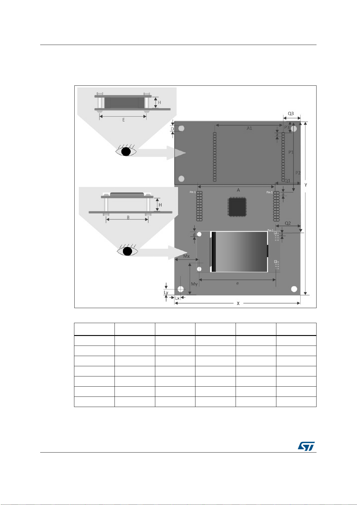
Mechanical dimensions UM2403
Appendix D Mechanical dimensions
Figure 53. Mechanical dimensions
Symbol Size (mm) Symbol Size (mm) Symbol Size (mm)
A 68.58 e 77.44 P2 111.76
A1 61.97 H 11 P3 10.41
a 2.54 Lx 5.715 Q1 24.12
B 36 Ly 5.715 Q2 17.70
D 3.5 Mx 19.08 Q3 16
d 3.2 My 23.81 X 114.3
E 47 P1 65.78 Y 172.72
76/78 UM2403 Rev 1
Table 41. Mechanical dimensions
Page 77

UM2403 Revision history
Revision history
Table 42. Document revision history
Date Revision Changes
7-Nov-2018 1 Initial version
UM2403 Rev 1 77/78
77
Page 78

UM2403
IMPORTANT NOTICE – PLEASE READ CAREFULLY
STMicroelectronics NV and its subsidiaries (“ST”) reserve the right to make changes, corrections, enhancements, modifications, and
improvements to ST products and/or to this document at any time without notice. Purchasers should obtain the latest relevant information on
ST products before placing orders. ST products are sold pursuant to ST’s terms and conditions of sale in place at the time of order
acknowledgement.
Purchasers are solely responsible for the choice, selection, and use of ST products and ST assumes no liability for application assistance or
the design of Purchasers’ products.
No license, express or implied, to any intellectual property right is granted by ST herein.
Resale of ST products with provisions different from the information set forth herein shall void any warranty granted by ST for such product.
ST and the ST logo are trademarks of ST. All other product or service names are the property of their respective owners.
Information in this document supersedes and replaces information previously supplied in any prior versions of this document.
© 2018 STMicroelectronics – All rights reserved
78/78 UM2403 Rev 1
 Loading...