现货库存、技术资料、百科信息、热点资讯,精彩尽在鼎好!
LM39
3
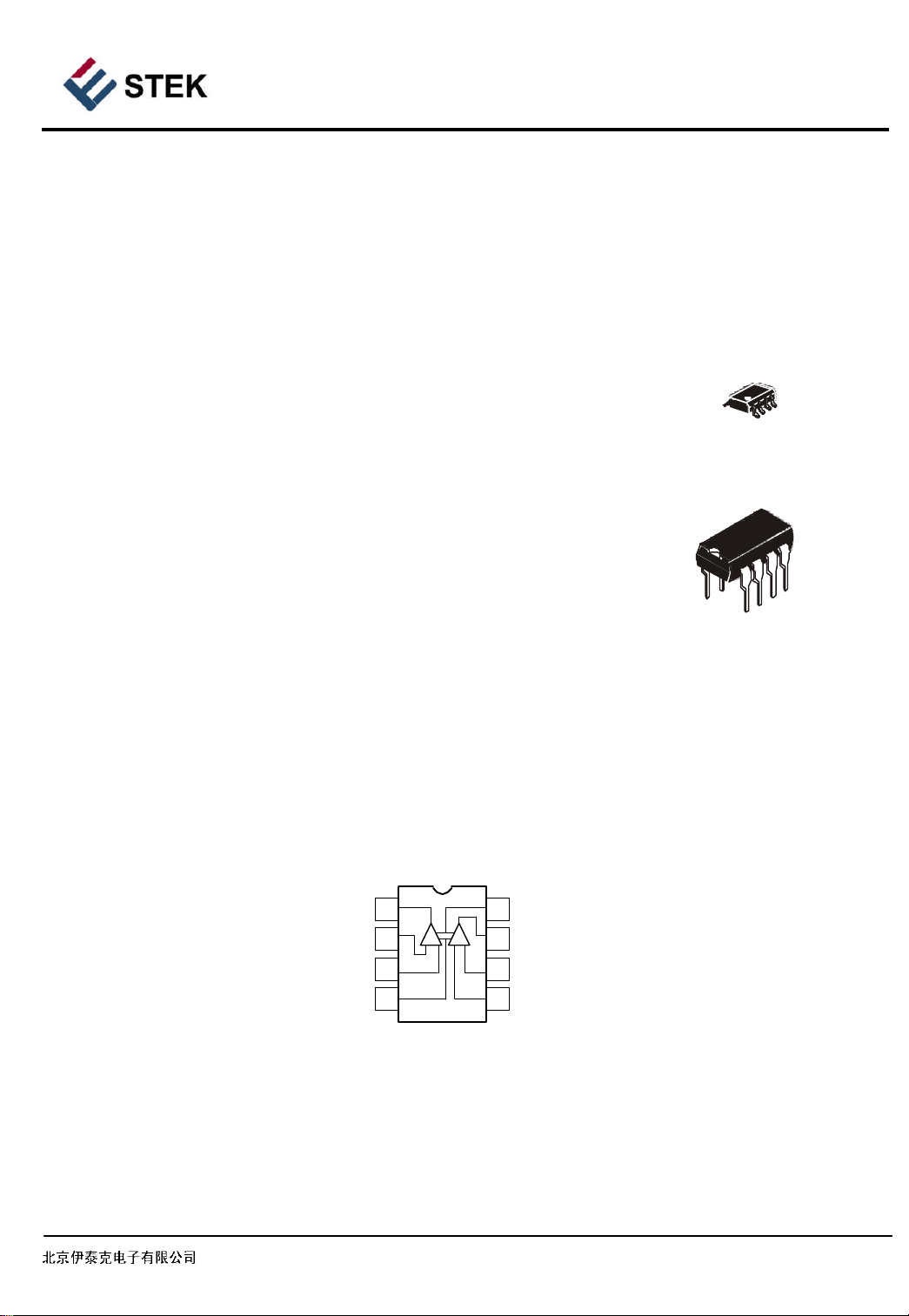
Description
rate
also
er
D
Features
Low o
utputsaturationvoltage
8
8
1
1
Package
Internal
Blo
c
k Di
gra
m
OUTPUT
A18
V+
INVERTING INPUT A
2AB
7
OUTPUT
B
NON-INVERTING INPUT A
36INVERTING INPUT B
GND
4
5
T
OP VIEW
1
BEIJING ESTEK ELECTRONICSCO.,LTD
The LM393 consists of two independent voltage comparators. These were designed specifically to ope
from a single power supply over a wide range of voltages. Operation from split power supplies is
possible and the low power supply current drain is independent of the magnitude of the pow
supply voltage. The outputs can be connected to other open-collector outputs to achieve wired-AN
relationships.
Wide supply voltage range
Low supplycurrent drain independent of supply
voltage.Low input biasing current
SOP-8
Low input offset current
Low input offset voltage
Input common-mode voltage range includes GND
Differentialinput voltage range equal to the power supplyvoltage
Output voltage compatible with TTL, MOS and CMOS
logic
DIP-8
NON-

LM39
3
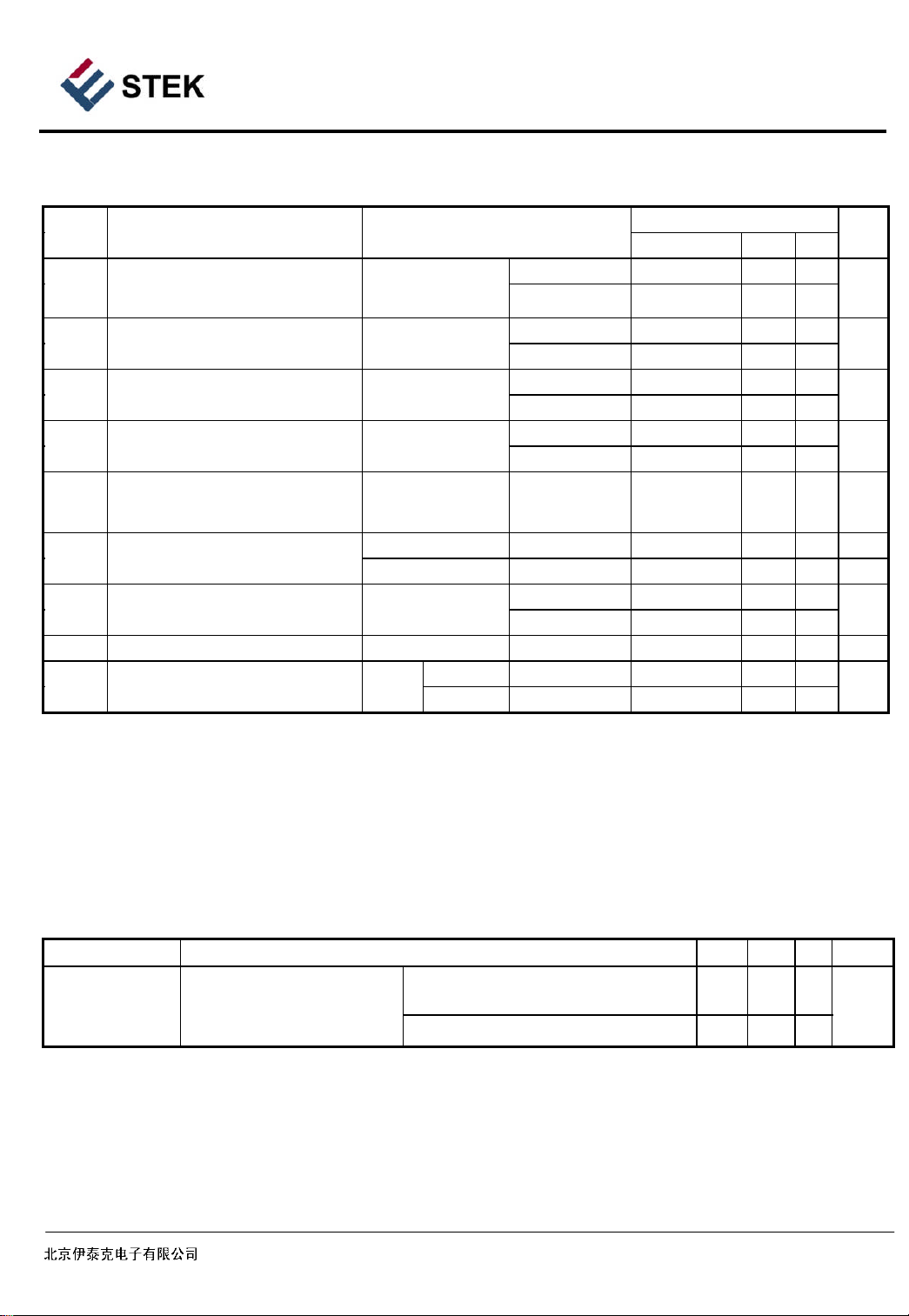
Electrical Characteristics
at
specified
free-air
temperature
,
Vcc=5V(unless
other
w
ise
noted)
SymbolParamete
r
Testconditions*
V
I
O
Input offset voltage
Vcc = 5 V to 30V,
LM393
Units
mV
min,
Full range
9
nA
V
A
signal differential voltage
amplification
Vo=1.4V to 11.4 V,
25
°С50
200
V/mV
lOHHigh-level output current
VOH=5 V, V
=1V,25°С0.150nA
VOH= 30V, V
I
D
=1V
Full
range
1µAVOLLow-
level output voltage
IOL= 4 mA,
V
I
D
=-1V
25
°С150
400
Full range
700mVlOLLow-
level output current
V
O
L
= 1.5V, V
I
D
=-1V25°С6mAICCSupply
current
RL=
∞
VCC= 5V25°С0.8
1
VCC= 30V
Full range
2.5
mA
Switching Charactristics
Vcc=5V, Т
=25°C
Paramete
r
Testcondition
sMinTypMaxUnits
Response time
RLconnected to 5V
through 5.1 k
Ω
,
100-mV input step
w
ith 5-mV overdrive
1.3
µs
CL=15pF* (See Note 1)
* CLincludes probe and jig capacitance.
Note 1: The response time specified is
the interval bet
w
een the input step function and the instant
w
hen the output crosses 1.4V.
BEIJING ESTEK ELECTRONICSCO.,LTD
2
l
Input offset current Vo=1.4 V
IO
I
Input bias current Vo=1.4 V
IB
V
Common-mode input voltage range**
ICR
Large-
VD
VIC= V
ICR
Vo=1.4 V
Vcc = 15 V,
RL≥ 15 kΩ to
ID
Min Typ Max
25 °С 2 5
25 °С 5 50
Full range 150
25 °С -25 -250
Full range -400
25°С 0 to Vcc-1.5
Full range 0 to Vcc - 2
nA
* Full range (MIN to MAX), for the LM393 is О °С to 70 °С . All characteristics are measured with zero common-mode input voltage
unless otherwise specified.
** The voltage at either input or common-mode should not be allowed to go negative by more than 0.3V. The upper end of the commonmode voltage range is VCC-1.5V, but either or both inputs can go to 30V without damage.
A
TTL-level input step 0.3

LM39
3
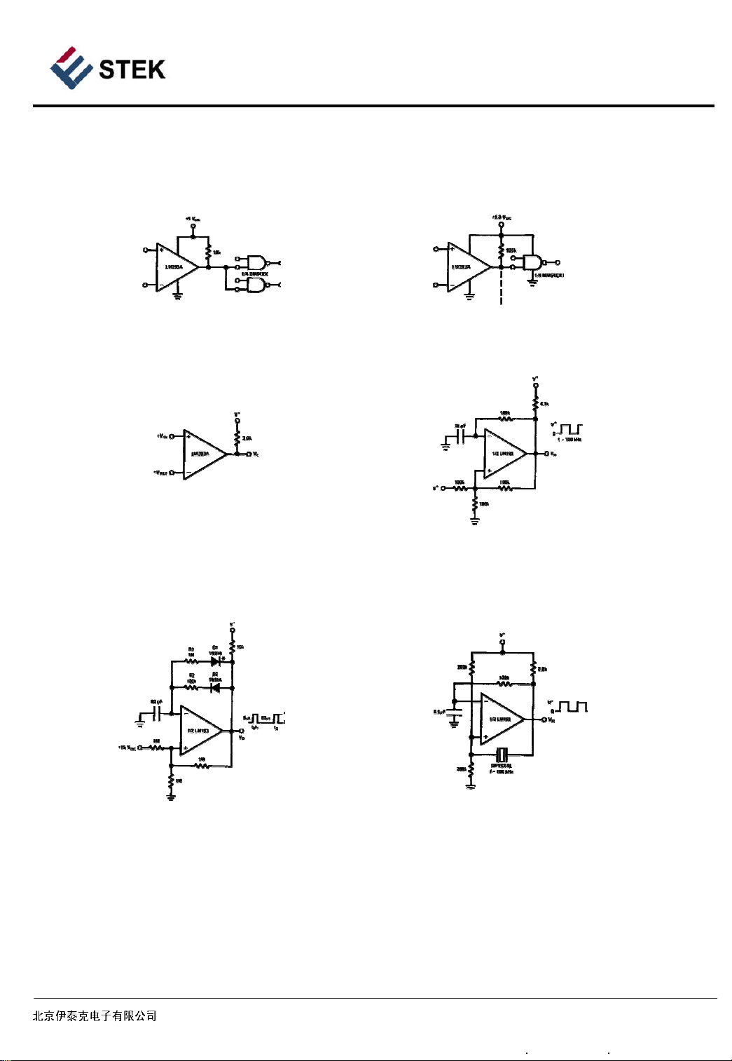
Typica
l ApplicationsCircui
t
Driving
TTL
Driving
CMOS
Squarewave
Oscillator
Basic
Comparator
Pulse
Generator
Crystal Controlled Oscillator
3
BEIJING ESTEK ELECTRONICSCO.,LTD

LM39
3
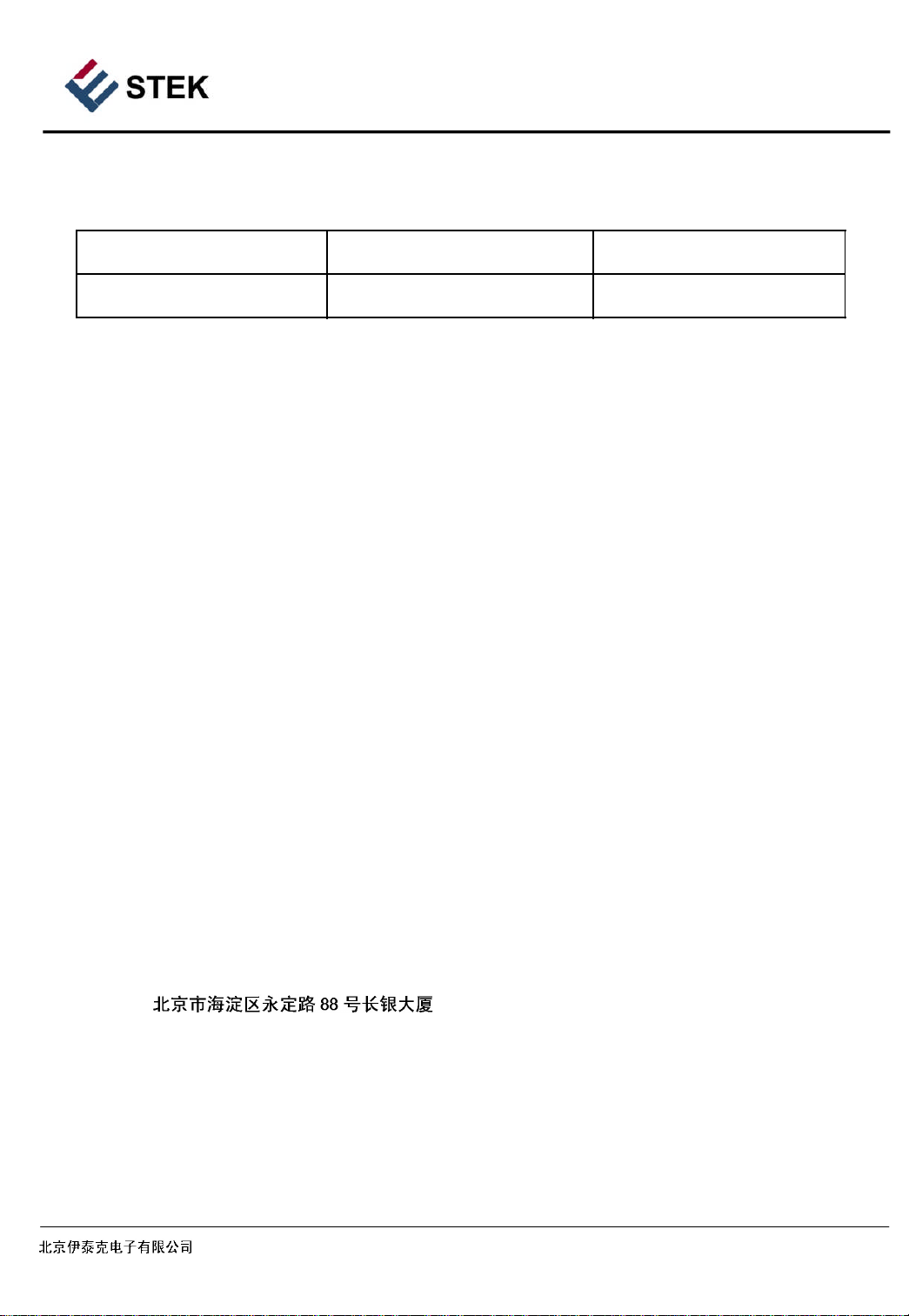
OrderingInformatio
n
ORDER
INNUMBERPACKAEMARKIN
LM393
DIP-8 / SOP
-8LM393
Address :
REV No:01
-
060820
4
BEIJING ESTEK ELECTRONICSCO.,LTD
G
G
G
Rm 6A07,Changyin Office Building ,No.88,Yong Ding Road,Hai Dian District ,Beijing
Postalcode:100039
Tel: 86-010-58895780 / 81 / 82 / 83 / 84 Fax : 010-58895793
Http://www.estek.com.cn
Email:sales@estek.com.cn
6A06--6A07
 Loading...