

现货库存、技术资料、百科信息、热点资讯,精彩尽在鼎好!
LM339
Description
The LM339 consists of four independent voltage comparators. These were designed specifically to operate
from a single power supply over a wide range of voltages. Operation from split power supplies is also possible
and the low power supply curr
outputs can be connected to other open
Features
§
Wide supply voltage range
Low supply current drain independent of supply voltage.
§
Low input biasing current
§
§
Low input offset current
Low input offset voltage
§
§
Input common- mode voltage range includes GND
§
Differential input voltage range equal to the power supply voltage
§
Low output saturation voltage
§
Output voltage compatible with TTL, MOS and CMOS logic
ent drain is independent of the magnitude of the power supply voltage. The
collector outputs to achieve wired
- -AND relationships.
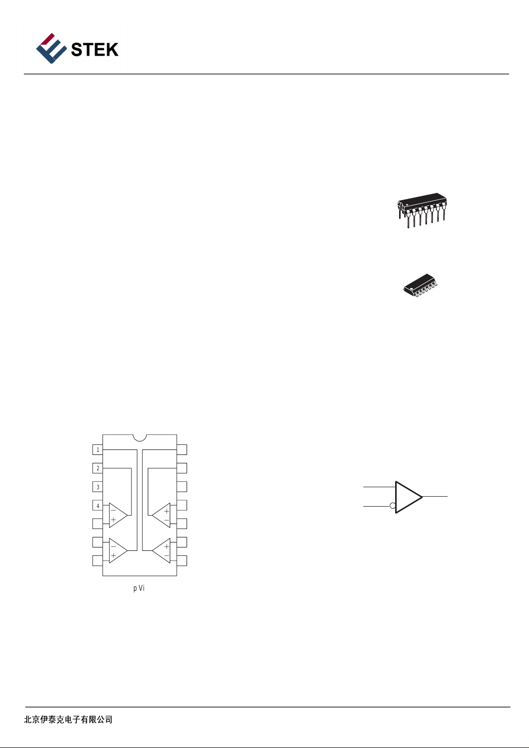
14
1
DIP - 14
14
1
SOP–14
Package
Internal Block Digram
PIN CONNECTIONS
Output 2
Output 1
– Input 1
+ Input 1
– Input 2
+ Input 2
1
2
3
V
CC
4
*
1
)
5
6
*
2
)
7
(Top View)
4
3
symbol (each comparator)
14
Output 3
13
Output 4
12
Gnd
11
+ Input 4
)
*
– Input 4
10
9
+ Input 3
)
*
8
– Input 3
IN+
OUT
IN–
BEIJING ESTEK ELECTRONICS CO.,LTD
1
Absolute Maximum Ratings
LM339
Symol
Power
V
CC
V 36 V
I
DR
V -0.3 to V
CR
I
t
Input
Input
Short-Circuit duration of Output 100 ms
S
Input
Junction
T
Plastic Package 150
Supply Voltages
Differential Voltage Range
Common Mode Voltage Range (1)
Current, per pin (2)
Temperature
Parameter Value
Single Supply
Split Supplies
36
±18
CC
50 mA
Tstg Storage Temperature -65 to +150
T
P
*
Maximum Ratings are those values which damage to the
Functional operation should be
Lead Temperature, 1mm from Case for 10 Seconds 260
L
Power
Plastic Package
D
Derate 25
Dissipation T
Above
V
°C
=+25 °C
A
beyond
restricted to the Recommended Operating Conditions.
device
1.0
8.0
may occur.
Notes:
1.
2. VIN
Power
Split Supplies.
<-0.3V.
IN
UNIT
V
V
°C
°C
°C
W
m °C
W/
Switching Characteristics
V
=5V, ÒA=25
CC
PARAMETER
Response time
* CL includes probe and jig capacitance.
NOTE : The response time specified is the interval between the input step function and the instant when the output
crosses 1.4V.
°C
R
connected to 5V through
L
5.1kΩ,
C
=15pF* (See Note )
L
TEST CONDITIONS
100-mV input step with 5 -mV overdrive 1.3
TTL-level input step
BEIJING ESTEK ELECTRONICS CO.,LTD
2
MIN TYP MAX UNIT
0.3
µ
s

Electrical Char acteristics
LM339
at specified free -air temperature, V
= 5V (unless otherwise noted)
CC
PARAMETER TEST CONDITIONS* MIN TYP MAX UNIT
V
VCC=5V to 30V
IO
Input offset voltage V
l
VO=1.4V
lO
Input offset current Full range 150
I
VO=1.4V
IB
Input bias current Full range -400
V
ICR
Common -mode input voltage range** Full range 0 to
A
VD
Large -signal differential voltage
amplification
I
V
OH
High -level output current VOH=30V, VID=1V Full range 1
V
I
OL
Low-level output voltage Full range 700
I
OL
Low-level output current
I
CC
Supply current VCC=30V Full range 2.5
* Full range (MIN to ), for the LM339 is 0
otherwise specified.
** The voltage at either input or common - mode should not be allowed to go negative by more than 0.3 V. The upper
end of the common - mode voltage range is VCC -1.5 V, but either or both inputs can go to 30 V without damage.
MAX
o
= V
IC
V
=15V, VO=1.4V to 11.4V,
CC
R
≥15kΩ to V
L
=5V, V
OH
=4mA, VID= -1V
OL
V
=1.5V, VID= -1V
OL
R
= ∞
L
to 70
o
C
, VO=1.4V Full range 9
I CRmin
CC
=1V
ID
. All characteristics are measured with zero common
C
VCC=5V
o
25
C
o
25
C
o
25
C
o
25
C
o
25
C
o
25
C
o
25
C
o
25
C
o
25
C
2 5 mV
5 50 nA
-25 -250 nA
0 to
Vcc-1.5
Vcc-2
50 200 V/mV
0.1 50 nA
150 400 mV
6 mA
0.8 2 mA
V
input voltage unless
-mode
µA
BEIJING ESTEK ELECTRONICS CO.,LTD
3

Typical Performance Characteristics
(VCC=1.5V, TA=+25°C (each comparator))
1.40
LM339
Figure 1. Normalized Input Offset Voltage
Figure 3. Output Sink Current versus
Output Saturation Voltage
Figure 2. Input Bias Current
BEIJING ESTEK ELECTRONICS CO.,LTD
4

Typical Applications Circuit
+ V
CC
LM339
+ V
V
CC
R3
10 k
in
R
ref
±
+
R1
R2
1.0 M
1
V
ref
10k
Figure 1. Inverting Comparator
V
ref
VH =
10 k
VCC R1
≈
R
ref
R1 / / R
≈
R1 / / R
R1/ / R
Rref / / /R1
V
O
+ R1
ref
ref
/ / R2
ref
+ R2
[V
O(max)
-V
O(min)
R
ref
V
ref
R1
Vi
]
R2
n
10 k
Figure . Noninverting Comparator
+ V
CC
10 k
±
+
R3
1.0 M
R2 ≈ R1 / / R
Amount of Hysteresis
VH =
R2 + R3
R2
ref
[(V
V
O
V
=
ref
O(max)
VCC R1
R
+ R1
ref
V
H
-V
O(min)
]
2
with Hystersis with Hysteresis
V
CC
R
V
in
V
ref
S
+
±
R1
Logic Device
CMOS
TTL
Figure Driving Logic
R
L
RS = Source
R
R1
≈
S
1/4 MC14001
1/4 MC7400
3.
Resistance
V
CC
(V)
+15
+5.0
R
k
100
10
+
C
V
CC
L
Ω
R2
330 k
Figure . Squarewave Oscillator
4
100 k
R4 330 k
±
+
R1
R3
330 k
VCC
4.0 V
.
10 k
V
O
V
CC
T1
T2
T1 = T2 = 0.69 RC
7.2
f
=
C(
F)
µ
R2 = R3 = R4
R2 // R3 // R4
BEIJING ESTEK ELECTRONICS CO.,LTD
5

LM339
+15 V
R1
8.2 k
V
in
D1
D1 prevents input from going negative by more than 0.6 V
R3
Figure 5
R4
220 k
6.8 k
R2
R5
3
10
. Zero Crossing Detector
R5
220 k
15 k
R3
R1 + R2 = R3
for small error in zero crossing
10 M
(Single Supply)
Ordering Information
10 k
V
≈0.4 V Peak
in(min)
V
O
V
in
V
CC
+
V
EE
Figure
for 1% phase
10 k
V
distortion
V
in
O
V
CC
V
O
V
EE
6. Zero Crossing Detector
(
∆Θ
).
V
in(min)
∆Θ
Θ
Θ
(Split Supplies)
PACKAG E MARKINGORDERING NUMBER
LM339M
Address :
Rm 6A07,Changyin Office Building ,No.88,Yong Ding Road,Hai Dian District ,Beijing
Postalcode:100039
Tel: 86-010-58895780 / 81 / 82 / 83 / 84
Http://www.estek.com.cn
Email:sales@estek.com.cn
SOP-14 / DIP-14
6A06--6A07
Fax : 010-58895793
LM339
REV No:01-060818
BEIJING ESTEK ELECTRONICS CO.,LTD
6
 Loading...