


MACH2 PARALLEL ATA
2.5-INCH SOLID STATE DRIVE
PRODUCT MANUAL

Export Administration Regulations
This document may contain technica l data con trolled by the U .S. Ex port Adm inistration Regula tions, and
may be subject to the approval of the U.S. Department of Commerce prior to export. Any export, directly or
indirectly, in contravention of the U.S. Export Administration Regu lation is prohibited.
Trademark Information
The STEC name, logo and design are trademarks of STEC Inc. No right, license, or interest to suc h
trademarks is granted hereunder, and you agree that no such right, license, or interest shall be asserted by
you with respect to such trademark. O ther produ ct and corpora te names me ntioned in this docume nt are
used for identification purposes only and may be trademarks or registered trademarks of their respective
companies.
Disclaimer of Liability
The performance information and specifications furnished in this document reflect the engineering
development objectives of STEC Inc. and should be us ed for comparative analysis and reference purposes.
The content of this document is accurate as of th e date of this publication; however, the inf ormation
contained herein, including but not limited to any instructions, description s and product specific ations, is
subject to change without prior notice.
STEC INC. (STEC) PROVIDES NO WARRANTY WITH REGARD TO THIS DOCUMENT OR
ANY OTHER INFORMATION CONTAINED HEREIN AND HEREBY EXPRESSLY DISCLAIMS
ANY IMPLIED WARRANTIES OF MERCHANTABILITY OR FITNESS FOR ANY
PARTICULAR PURPOSE WITH REGARD TO ANY OF THE FOREGOING. STEC INC.
ASSUMES NO LIABILITY FOR ANY DAMAGES INCURRED DIRECTLY OR INDIRECTLY
FROM ANY TECHNICAL OR TYPOGRAPHICAL ERRORS OR OMMISSIONS CONTAINED
HEREIN. IN NO EVENT SHALL STEC INC. BE LIABLE FOR ANY INCIDENTAL,
CONSEQUENTIAL, SPECIAL, OR EXEMPLARY DAMAGES, WHETHER BASED ON TORT,
CONTRACT OR OTHERWISE, ARISING OUT OF OR IN CONNECTION WITH THIS
DOCUMENT OR ANY OTHER INFORMATION CONTAINED HEREIN OR THE USE
THEREOF.
Copyright Notice
Copyright © 2007 by STEC Inc. All rights reserved. Informa ti on c ontained in this document, including but
not limited to any instructions, descriptions and product specifications, is proprietary to STEC Inc. and shall
not be modified, used, copied, reproduced or disclose d in whole or in part, in any form or by any mean s,
electronic or mechanical, for any purpose, without the wri tt en c onse nt of STEC Inc.
ii MACH2 2.5-Inch ATA Solid State Drive
PRELIMINARY/CONFIDENTIAL
CONVENTIONS
The following icons are used throughout this document to identify additional information
of which the reader should be aware.
SHOCK HAZARD: This icon indicates the danger of
an electrical shock that may harm or otherwise prove
fatal to the user.
CAUTION: This icon indicates the exis tence of a
hazard that could result in equipment or prop erty
damage or equipment failure if the safety instruction
is not observed.
ELECTROSTATIC DISCHARGE: This icon indicates
the possible presence of Electrostatic Discharge
(ESD or “static electricity”) that may harm the
internal electronic components. The us er is a dvised
to handle the device only after discharging any
possible electrostatic buildup that may be present.
NOTE: This icon identifies information that relates to
the safe operation of the equipment or related items.
TIP: This icon identifies helpful hints and tips.
MACH2 2.5-Inch ATA Solid State Drive iii

PRELIMINARY/CONFIDENTIAL
iv MACH2 2.5-Inch ATA Solid State Drive

PRELIMINARY/CONFIDENTIAL
REVISION HISTORY
Revision Status Summary Sheet
Revision Date Sheet(s) Affected
1.0 07/10/2007 Official release.
1.1 08/10/2007 Page 59: Warranty period updated.
1.2 10/10/2007 Page 53: Updated contact and ordering information.
1.3 11/01/2007 Page 33: Added “Identify Device Command Output” topic and table.
1.4 11/09/2007 Pages 23 - 24. Added S.M.A.R.T. Support, Commands and Attributes topics
1.5 01/24/2008 Pages 2 and 7: Corrected Burst Transfer Rate to 100MB/sec.
MACH2 2.5-Inch ATA Solid State Drive v
respectively.

PRELIMINARY/CONFIDENTIAL
vi MACH2 2.5-Inch ATA Sol id State Drive

PRELIMINARY/CONFIDENTIAL
TABLE OF CONTENTS
Conventions . . . . . . . . . . . . . . . . . . . . . . . . . . . . . . . . . . . . . . . . . . . . . . . . . . . . iii
Revision History. . . . . . . . . . . . . . . . . . . . . . . . . . . . . . . . . . . . . . . . . . . . . . . . . .v
List of Tables . . . . . . . . . . . . . . . . . . . . . . . . . . . . . . . . . . . . . . . . . . . . . . . . . . .xii
List of Figures . . . . . . . . . . . . . . . . . . . . . . . . . . . . . . . . . . . . . . . . . . . . . . . . . xiv
Scope . . . . . . . . . . . . . . . . . . . . . . . . . . . . . . . . . . . . . . . . . . . . . . . . . . . . . . . . . .1
Overview . . . . . . . . . . . . . . . . . . . . . . . . . . . . . . . . . . . . . . . . . . . . . . . . . . . . . . . . . . . . . . . . . .1
Audience . . . . . . . . . . . . . . . . . . . . . . . . . . . . . . . . . . . . . . . . . . . . . . . . . . . . . . . . . . . . . . . . . .1
Feature Overview. . . . . . . . . . . . . . . . . . . . . . . . . . . . . . . . . . . . . . . . . . . . . . . . . . . . . . . . . . . .2
Standards and Reference Documents. . . . . . . . . . . . . . . . . . . . . . . . . . . . . . . . . . . . . . . . . . . .3
Commercial Standards . . . . . . . . . . . . . . . . . . . . . . . . . . . . . . . . . . . . . . . . . . . . . . . . . . .3
Reference Documents. . . . . . . . . . . . . . . . . . . . . . . . . . . . . . . . . . . . . . . . . . . . . . . . . . . .3
Manufacturing . . . . . . . . . . . . . . . . . . . . . . . . . . . . . . . . . . . . . . . . . . . . . . . . . . . . . . . . . . . . . . 3
Product Description. . . . . . . . . . . . . . . . . . . . . . . . . . . . . . . . . . . . . . . . . . . . . . .4
General Description. . . . . . . . . . . . . . . . . . . . . . . . . . . . . . . . . . . . . . . . . . . . . . . . . . . . . . . . . .4
ATA Interface. . . . . . . . . . . . . . . . . . . . . . . . . . . . . . . . . . . . . . . . . . . . . . . . . . . . . . . . . . . . . . .4
Drive Capacities. . . . . . . . . . . . . . . . . . . . . . . . . . . . . . . . . . . . . . . . . . . . . . . . . . . . . . . . . . . . .4
Performance . . . . . . . . . . . . . . . . . . . . . . . . . . . . . . . . . . . . . . . . . . . . . . . . . . . . . . . . . . . . . . .4
Performance Characteristics . . . . . . . . . . . . . . . . . . . . . . . . . . . . . . . . . . . . . . .5
ATA Modes . . . . . . . . . . . . . . . . . . . . . . . . . . . . . . . . . . . . . . . . . . . . . . . . . . . . . . . . . . . . . . . .5
Endurance . . . . . . . . . . . . . . . . . . . . . . . . . . . . . . . . . . . . . . . . . . . . . . . . . . . . . . . . . . . . . . . . .5
Wear-Leveling . . . . . . . . . . . . . . . . . . . . . . . . . . . . . . . . . . . . . . . . . . . . . . . . . . . . . . . . . . . . . .5
Bad-Block Management. . . . . . . . . . . . . . . . . . . . . . . . . . . . . . . . . . . . . . . . . . . . . . . . . . . . . . .6
Data Retention. . . . . . . . . . . . . . . . . . . . . . . . . . . . . . . . . . . . . . . . . . . . . . . . . . . . . . . . . . . . . .6
Error Detection and Correction . . . . . . . . . . . . . . . . . . . . . . . . . . . . . . . . . . . . . . . . . . . . . . . . .6
Reliability . . . . . . . . . . . . . . . . . . . . . . . . . . . . . . . . . . . . . . . . . . . . . . . . . . . . . . . . . . . . . . . . . .6
Error Rates. . . . . . . . . . . . . . . . . . . . . . . . . . . . . . . . . . . . . . . . . . . . . . . . . . . . . . . . . . . . .7
Built-In Self Test (BIST). . . . . . . . . . . . . . . . . . . . . . . . . . . . . . . . . . . . . . . . . . . . . . . . . . .7
Mount Time . . . . . . . . . . . . . . . . . . . . . . . . . . . . . . . . . . . . . . . . . . . . . . . . . . . . . . . . . . . . 7
MACH2 2.5-Inch ATA Solid State Drive vii

PRELIMINARY/CONFIDENTIAL
Seek Time . . . . . . . . . . . . . . . . . . . . . . . . . . . . . . . . . . . . . . . . . . . . . . . . . . . . . . . . . . . . .7
Data Transfer Rates . . . . . . . . . . . . . . . . . . . . . . . . . . . . . . . . . . . . . . . . . . . . . . . . . . . . . 7
Repairs . . . . . . . . . . . . . . . . . . . . . . . . . . . . . . . . . . . . . . . . . . . . . . . . . . . . . . . . . . . . . . . 8
Preventative Maintenance. . . . . . . . . . . . . . . . . . . . . . . . . . . . . . . . . . . . . . . . . . . . . . . . .8
Electrical Specifications . . . . . . . . . . . . . . . . . . . . . . . . . . . . . . . . . . . . . . . . . . 9
Power Requirements. . . . . . . . . . . . . . . . . . . . . . . . . . . . . . . . . . . . . . . . . . . . . . . . . . . . . . . . .9
Power Consumption . . . . . . . . . . . . . . . . . . . . . . . . . . . . . . . . . . . . . . . . . . . . . . . . . . . . . . . . .9
Start-Up Time and Current Draw. . . . . . . . . . . . . . . . . . . . . . . . . . . . . . . . . . . . . . . . . . . . . . . 10
Activity LED. . . . . . . . . . . . . . . . . . . . . . . . . . . . . . . . . . . . . . . . . . . . . . . . . . . . . . . . . . . . . . .10
Power-On Ready Time . . . . . . . . . . . . . . . . . . . . . . . . . . . . . . . . . . . . . . . . . . . . . . . . . . . . . .11
Power Savings Commands. . . . . . . . . . . . . . . . . . . . . . . . . . . . . . . . . . . . . . . . . . . . . . . . . . .11
Power Mode at Power On . . . . . . . . . . . . . . . . . . . . . . . . . . . . . . . . . . . . . . . . . . . . . . . . . . . . 11
Grounding . . . . . . . . . . . . . . . . . . . . . . . . . . . . . . . . . . . . . . . . . . . . . . . . . . . . . . . . . . . . . . . . 11
Interface Specifications. . . . . . . . . . . . . . . . . . . . . . . . . . . . . . . . . . . . . . . . . . 12
SSD Operation . . . . . . . . . . . . . . . . . . . . . . . . . . . . . . . . . . . . . . . . . . . . . . . . . . . . . . . . . . . . 12
Write Operations . . . . . . . . . . . . . . . . . . . . . . . . . . . . . . . . . . . . . . . . . . . . . . . . . . . . . . . 12
Read Requests . . . . . . . . . . . . . . . . . . . . . . . . . . . . . . . . . . . . . . . . . . . . . . . . . . . . . . . . 12
Primary and Secondary Modes. . . . . . . . . . . . . . . . . . . . . . . . . . . . . . . . . . . . . . . . . . . . . . . .13
I/O Primary and Secondary ATA (IDE) Modes . . . . . . . . . . . . . . . . . . . . . . . . . . . . . . . .13
Addressing Modes. . . . . . . . . . . . . . . . . . . . . . . . . . . . . . . . . . . . . . . . . . . . . . . . . . . . . . 13
44-Pin ATA Bus Connector . . . . . . . . . . . . . . . . . . . . . . . . . . . . . . . . . . . . . . . . . . . . . . . . . . . 14
Connector Pinout Signals . . . . . . . . . . . . . . . . . . . . . . . . . . . . . . . . . . . . . . . . . . . . . . . . . . . .15
ATA Commands . . . . . . . . . . . . . . . . . . . . . . . . . . . . . . . . . . . . . . . . . . . . . . . . 17
Overview . . . . . . . . . . . . . . . . . . . . . . . . . . . . . . . . . . . . . . . . . . . . . . . . . . . . . . . . . . . . . . . . .17
Standard ATA Commands. . . . . . . . . . . . . . . . . . . . . . . . . . . . . . . . . . . . . . . . . . . . . . . . . . . .17
Standard ATA Command Summary . . . . . . . . . . . . . . . . . . . . . . . . . . . . . . . . . . . . . . . . . . . .19
S.M.A.R.T. Support . . . . . . . . . . . . . . . . . . . . . . . . . . . . . . . . . . . . . . . . . . . . . . . . . . . . .24
S.M.A.R.T. Commands . . . . . . . . . . . . . . . . . . . . . . . . . . . . . . . . . . . . . . . . . . . . . . . . . . 24
S.M.A.R.T. Attributes. . . . . . . . . . . . . . . . . . . . . . . . . . . . . . . . . . . . . . . . . . . . . . . . . . . . 25
viii MACH2 2.5-Inch ATA Solid State Drive

PRELIMINARY/CONFIDENTIAL
Identify Device Information . . . . . . . . . . . . . . . . . . . . . . . . . . . . . . . . . . . . . . . . . . . . . . . . . . .25
Identify Device Command Output . . . . . . . . . . . . . . . . . . . . . . . . . . . . . . . . . . . . . . . . . . . . . . 35
Vendor-Specific ATA Commands . . . . . . . . . . . . . . . . . . . . . . . . . . . . . . . . . . . . . . . . . . . . . .36
Physical Characteristics . . . . . . . . . . . . . . . . . . . . . . . . . . . . . . . . . . . . . . . . . .37
General Physical Characteristics. . . . . . . . . . . . . . . . . . . . . . . . . . . . . . . . . . . . . . . . . . . . . . . 37
Materials . . . . . . . . . . . . . . . . . . . . . . . . . . . . . . . . . . . . . . . . . . . . . . . . . . . . . . . . . . . . . . . . .37
Drive Assembly Weight . . . . . . . . . . . . . . . . . . . . . . . . . . . . . . . . . . . . . . . . . . . . . . . . . . . . . .37
Storage Capacities. . . . . . . . . . . . . . . . . . . . . . . . . . . . . . . . . . . . . . . . . . . . . . . . . . . . . . . . . .37
Exterior Dimensions. . . . . . . . . . . . . . . . . . . . . . . . . . . . . . . . . . . . . . . . . . . . . . . . . . . . . . . . .38
Connector Location . . . . . . . . . . . . . . . . . . . . . . . . . . . . . . . . . . . . . . . . . . . . . . . . . . . . . . . . .39
Environmental Characteristics . . . . . . . . . . . . . . . . . . . . . . . . . . . . . . . . . . . . .40
Overview . . . . . . . . . . . . . . . . . . . . . . . . . . . . . . . . . . . . . . . . . . . . . . . . . . . . . . . . . . . . . . . . .40
Operating Temperatures . . . . . . . . . . . . . . . . . . . . . . . . . . . . . . . . . . . . . . . . . . . . . . . . . . . . .40
Operating Requirements . . . . . . . . . . . . . . . . . . . . . . . . . . . . . . . . . . . . . . . . . . . . . . . . . . . . .40
Non-Operating Requirements . . . . . . . . . . . . . . . . . . . . . . . . . . . . . . . . . . . . . . . . . . . . . . . . .41
Relative Humidity. . . . . . . . . . . . . . . . . . . . . . . . . . . . . . . . . . . . . . . . . . . . . . . . . . . . . . . . . . .41
Altitude Parameters. . . . . . . . . . . . . . . . . . . . . . . . . . . . . . . . . . . . . . . . . . . . . . . . . . . . . . . . .41
Restriction of Hazardous Materials . . . . . . . . . . . . . . . . . . . . . . . . . . . . . . . . . . . . . . . . . . . . . 42
Shock and Vibration. . . . . . . . . . . . . . . . . . . . . . . . . . . . . . . . . . . . . . . . . . . . . . . . . . . . . . . . .42
Failure Criteria. . . . . . . . . . . . . . . . . . . . . . . . . . . . . . . . . . . . . . . . . . . . . . . . . . . . . . . . .42
Random Vibration . . . . . . . . . . . . . . . . . . . . . . . . . . . . . . . . . . . . . . . . . . . . . . . . . . . . . . 4 2
Shock. . . . . . . . . . . . . . . . . . . . . . . . . . . . . . . . . . . . . . . . . . . . . . . . . . . . . . . . . . . . . . . . 43
Drop Testing . . . . . . . . . . . . . . . . . . . . . . . . . . . . . . . . . . . . . . . . . . . . . . . . . . . . . . . . . .43
Conformal Coating (Optional) . . . . . . . . . . . . . . . . . . . . . . . . . . . . . . . . . . . . . . . . . . . . .43
Installation . . . . . . . . . . . . . . . . . . . . . . . . . . . . . . . . . . . . . . . . . . . . . . . . . . . . .44
System Requirements . . . . . . . . . . . . . . . . . . . . . . . . . . . . . . . . . . . . . . . . . . . . . . . . . . . . . . .44
Drive Configuration . . . . . . . . . . . . . . . . . . . . . . . . . . . . . . . . . . . . . . . . . . . . . . . . . . . . . . . . .45
Jumper Pins. . . . . . . . . . . . . . . . . . . . . . . . . . . . . . . . . . . . . . . . . . . . . . . . . . . . . . . . . . . . . . .45
Drive Orientation . . . . . . . . . . . . . . . . . . . . . . . . . . . . . . . . . . . . . . . . . . . . . . . . . . . . . . . . . . .46
MACH2 2.5-Inch ATA Solid State Drive ix

PRELIMINARY/CONFIDENTIAL
Primary Heat Generation Area . . . . . . . . . . . . . . . . . . . . . . . . . . . . . . . . . . . . . . . . . . . . . . . .47
Cooling Requirements. . . . . . . . . . . . . . . . . . . . . . . . . . . . . . . . . . . . . . . . . . . . . . . . . . . . . . .48
Installation Dimensions . . . . . . . . . . . . . . . . . . . . . . . . . . . . . . . . . . . . . . . . . . . . . . . . . . . . . . 49
Mounting Hole Locations. . . . . . . . . . . . . . . . . . . . . . . . . . . . . . . . . . . . . . . . . . . . . . . . . . . . .50
Drive Installation . . . . . . . . . . . . . . . . . . . . . . . . . . . . . . . . . . . . . . . . . . . . . . . . . . . . . . . . . . .51
Grounding Requirements . . . . . . . . . . . . . . . . . . . . . . . . . . . . . . . . . . . . . . . . . . . . . . . . . . . . 51
Operating System Specifications. . . . . . . . . . . . . . . . . . . . . . . . . . . . . . . . . . . . . . . . . . . . . . . 52
Microsoft OS Compatibility . . . . . . . . . . . . . . . . . . . . . . . . . . . . . . . . . . . . . . . . . . . . . . . 52
Non-Microsoft OS Compatibility. . . . . . . . . . . . . . . . . . . . . . . . . . . . . . . . . . . . . . . . . . . .52
System POST, Boot and Resume Times . . . . . . . . . . . . . . . . . . . . . . . . . . . . . . . . . . . . 52
Diagnostic Software. . . . . . . . . . . . . . . . . . . . . . . . . . . . . . . . . . . . . . . . . . . . . . . . . . . . . . . . .52
Default S.M.A.R.T. Settings. . . . . . . . . . . . . . . . . . . . . . . . . . . . . . . . . . . . . . . . . . . . . . . . . . .53
Regulatory Compliance . . . . . . . . . . . . . . . . . . . . . . . . . . . . . . . . . . . . . . . . . . 54
Marks, Approvals and Documentation. . . . . . . . . . . . . . . . . . . . . . . . . . . . . . . . . . . . . . . . . . . 54
Electromagnetic Susceptibility. . . . . . . . . . . . . . . . . . . . . . . . . . . . . . . . . . . . . . . . . . . . . . . . . 55
Electromagnetic Compatibility. . . . . . . . . . . . . . . . . . . . . . . . . . . . . . . . . . . . . . . . . . . . . . . . .55
CB Certificate and CB Report . . . . . . . . . . . . . . . . . . . . . . . . . . . . . . . . . . . . . . . . . . . . . . . . . 55
Declaration of Conformity . . . . . . . . . . . . . . . . . . . . . . . . . . . . . . . . . . . . . . . . . . . . . . . . . . . .56
Radio Frequency Emissions . . . . . . . . . . . . . . . . . . . . . . . . . . . . . . . . . . . . . . . . . . . . . . . . . . 56
Radio Frequency Immunity Requirements . . . . . . . . . . . . . . . . . . . . . . . . . . . . . . . . . . . . . . . 56
EMI Test Site Correlation. . . . . . . . . . . . . . . . . . . . . . . . . . . . . . . . . . . . . . . . . . . . . . . . . . . . .57
Verification Samples . . . . . . . . . . . . . . . . . . . . . . . . . . . . . . . . . . . . . . . . . . . . . . . . . . . . . . . . 57
Verification Testing . . . . . . . . . . . . . . . . . . . . . . . . . . . . . . . . . . . . . . . . . . . . . . . . . . . . . . . . .57
Electrostatic Discharge (ESD). . . . . . . . . . . . . . . . . . . . . . . . . . . . . . . . . . . . . . . . . . . . . . . . .58
Acceptance Criteria Definitions . . . . . . . . . . . . . . . . . . . . . . . . . . . . . . . . . . . . . . . . . . . . . . . .58
x MACH2 2.5-Inch AT A Solid State Drive

PRELIMINARY/CONFIDENTIAL
Contact and Ordering Information . . . . . . . . . . . . . . . . . . . . . . . . . . . . . . . . . .59
Contact Information . . . . . . . . . . . . . . . . . . . . . . . . . . . . . . . . . . . . . . . . . . . . . . . . . . . . . . . . .59
Ordering Information . . . . . . . . . . . . . . . . . . . . . . . . . . . . . . . . . . . . . . . . . . . . . . . . . . . . . . . .59
Index . . . . . . . . . . . . . . . . . . . . . . . . . . . . . . . . . . . . . . . . . . . . . . . . . . . . . . . . . .61
Certification and Warranty . . . . . . . . . . . . . . . . . . . . . . . . . . Inside Back Cover
MACH2 2.5-Inch ATA Solid State Drive xi

PRELIMINARY/CONFIDENTIAL
LIST OF TABLES
1. ATA Operating Modes . . . . . . . . . . . . . . . . . . . . . . . . . . . . . . . . . . . . . . . . . . . . . . . . . 5
2. Endurance Conditions . . . . . . . . . . . . . . . . . . . . . . . . . . . . . . . . . . . . . . . . . . . . . . . . . 5
3. Error Limits. . . . . . . . . . . . . . . . . . . . . . . . . . . . . . . . . . . . . . . . . . . . . . . . . . . . . . . . . . 7
4. Data Transfer Rates. . . . . . . . . . . . . . . . . . . . . . . . . . . . . . . . . . . . . . . . . . . . . . . . . . . 7
5. SSD Power Requirements . . . . . . . . . . . . . . . . . . . . . . . . . . . . . . . . . . . . . . . . . . . . . . 9
6. SSD Typical Power Consumption . . . . . . . . . . . . . . . . . . . . . . . . . . . . . . . . . . . . . . . . 9
7. Start-Up Time and Current Draw . . . . . . . . . . . . . . . . . . . . . . . . . . . . . . . . . . . . . . . . 10
8. ATA (IDE) Bus Addressing Modes. . . . . . . . . . . . . . . . . . . . . . . . . . . . . . . . . . . . . . . 13
9. ATA Connector Pinout Configuration . . . . . . . . . . . . . . . . . . . . . . . . . . . . . . . . . . . . . 15
10. Supported ATA Commands . . . . . . . . . . . . . . . . . . . . . . . . . . . . . . . . . . . . . . . . . . . . 17
11. ATA Command Summary. . . . . . . . . . . . . . . . . . . . . . . . . . . . . . . . . . . . . . . . . . . . . . 19
12. S.M.A.R.T. Command Values . . . . . . . . . . . . . . . . . . . . . . . . . . . . . . . . . . . . . . . . . . 24
13. Supported S.M.A.R.T. Attributes . . . . . . . . . . . . . . . . . . . . . . . . . . . . . . . . . . . . . . . . 25
14. Identify Device Information. . . . . . . . . . . . . . . . . . . . . . . . . . . . . . . . . . . . . . . . . . . . . 26
15. ECh Command Output. . . . . . . . . . . . . . . . . . . . . . . . . . . . . . . . . . . . . . . . . . . . . . . . 35
16. SSD Capacities . . . . . . . . . . . . . . . . . . . . . . . . . . . . . . . . . . . . . . . . . . . . . . . . . . . . . 37
17. Drive Assembly Dimensions. . . . . . . . . . . . . . . . . . . . . . . . . . . . . . . . . . . . . . . . . . . . 38
18. Operating Temperatures . . . . . . . . . . . . . . . . . . . . . . . . . . . . . . . . . . . . . . . . . . . . . . 40
19. Operating Requirements . . . . . . . . . . . . . . . . . . . . . . . . . . . . . . . . . . . . . . . . . . . . . . 40
20. Non-Operating Requirements. . . . . . . . . . . . . . . . . . . . . . . . . . . . . . . . . . . . . . . . . . . 41
21. Relative Humidity Criteria. . . . . . . . . . . . . . . . . . . . . . . . . . . . . . . . . . . . . . . . . . . . . . 41
22. Operating and Non-Operating Altitudes . . . . . . . . . . . . . . . . . . . . . . . . . . . . . . . . . . . 41
23. Random Vibration Levels . . . . . . . . . . . . . . . . . . . . . . . . . . . . . . . . . . . . . . . . . . . . . . 42
24. Shock Test Results. . . . . . . . . . . . . . . . . . . . . . . . . . . . . . . . . . . . . . . . . . . . . . . . . . . 43
25. ATA (IDE) Cable Requirements . . . . . . . . . . . . . . . . . . . . . . . . . . . . . . . . . . . . . . . . . 44
26. Default SMART Settings. . . . . . . . . . . . . . . . . . . . . . . . . . . . . . . . . . . . . . . . . . . . . . . 53
27. Regulatory Marks and Documentation. . . . . . . . . . . . . . . . . . . . . . . . . . . . . . . . . . . . 54
xii MACH2 2.5-Inch ATA Solid State Drive

PRELIMINARY/CONFIDENTIAL
28. EMI Specification Limits . . . . . . . . . . . . . . . . . . . . . . . . . . . . . . . . . . . . . . . . . . . . . . . 56
29. ESD Requirements. . . . . . . . . . . . . . . . . . . . . . . . . . . . . . . . . . . . . . . . . . . . . . . . . . . 58
30. Acceptance Criteria Definitions. . . . . . . . . . . . . . . . . . . . . . . . . . . . . . . . . . . . . . . . . . 58
MACH2 2.5-Inch ATA Solid State Drive xiii

PRELIMINARY/CONFIDENTIAL
LIST OF FIGURES
1. The MACH2 2.5-Inch ATA Solid State Drive . . . . . . . . . . . . . . . . . . . . . . . . . . . . . . . . 1
2. Start-Up Current Draw . . . . . . . . . . . . . . . . . . . . . . . . . . . . . . . . . . . . . . . . . . . . . . . . 10
3. 44-pin ATA (IDE) Bus Connector . . . . . . . . . . . . . . . . . . . . . . . . . . . . . . . . . . . . . . . . 14
4. SDD Exterior Dimensions. . . . . . . . . . . . . . . . . . . . . . . . . . . . . . . . . . . . . . . . . . . . . . 38
5. ATA Connector Location . . . . . . . . . . . . . . . . . . . . . . . . . . . . . . . . . . . . . . . . . . . . . . 39
6. Primary/Secondary Jumper Settings . . . . . . . . . . . . . . . . . . . . . . . . . . . . . . . . . . . . . 45
7. Possible Drive Orientations . . . . . . . . . . . . . . . . . . . . . . . . . . . . . . . . . . . . . . . . . . . . 46
8. Primary Heat Generation Area. . . . . . . . . . . . . . . . . . . . . . . . . . . . . . . . . . . . . . . . . . 47
9. Suggested Air Flow Patterns for Cooling . . . . . . . . . . . . . . . . . . . . . . . . . . . . . . . . . . 48
10. Exterior Mounting Specifications . . . . . . . . . . . . . . . . . . . . . . . . . . . . . . . . . . . . . . . . 49
11. Mounting Hole Locations . . . . . . . . . . . . . . . . . . . . . . . . . . . . . . . . . . . . . . . . . . . . . . 50
xiv MACH2 2.5-Inch AT A Solid State Drive

PRELIMINARY/CONFIDENTIAL
SCOPE
Overview
Figure 1. The MACH2 2.5-Inch ATA Solid State Drive
This datasheet describes the applications, specifications, and installation of the MACH2 2.5-inch ATA
Solid State Drive (SSD). See Figure 1.
Audience
This datasheet is intended for system engineers or system designers employed by an Original
Equipment Manufacturer (OEM). This datasheet was therefore written specifically for a technically
advanced audience; it is not intended for end-users that will eventually purchase the commercially
available product. The user, as referenced throughout this document, is primarily concerned with
industrial, commercial, or military computing applications.
MACH2 2.5-Inch ATA Solid State Drive 1

PRELIMINARY/CONFIDENTIAL
Feature Overview
Feature Description
Form Factor 2.5-Inch
ATA Interface ATA 6 or higher
Connector 44-Pin IDE/ATA (40/80 conductor)
Drive Capacities 4, 8, 16 and 32 gigabytes
Operating Voltage 5.0V +/-5%
Operating Temperature -40oC to +85oC
Average Latency 0.5 msec
Burst Transfer Rate 100MB/sec
Sustained Read Throughput 35MB/sec
Sustained Write Throughput 25MB/sec
Wear-Levelling Dynamic and static algorithms
Bad-Block Management 2% reserve of total flash capacity
EDC/ECC Correction: up to 4 bytes; Detection: up to 5 bytes
Data Retention 10 years storage
RoHS Compliance Pb-free components
Warranty 2 years
2 MACH2 2.5-Inch ATA Solid State Drive

PRELIMINARY/CONFIDENTIAL
Standards and Reference Documents
This section discusses the formal standards that may apply to the SSD, including electrical product
standards and military information security standards. In addition, this section lists reference
documents relevant to the ATA protocols used for the SSD.
Commercial Standards
The SSD complies, in whole or in part, with the following commercial standards:
S/NZS 3548 Class B Underwriters Laboratories (UL)
BSMI CNS 13438 Class B NEBS Level 3
CAN/CAS-V3/2001.04 (VCCI) IEC 61000-4-2
CE (Conformite Europenne) IEC 61000-4-3
CISPR 22 Class B IEC 61000-4-4
EN 55022 Class B IEC 61000-4-5
EN 61000-3-2 IEC 61000-4-6
EN 61000-3-3 IEC 61000-4-8
FCC Part 15 Class B IEC 61000-4-11
Reference Documents
The following list of ANSI documents are relevant to the SSD:
INCITS T13 1321 D Information Technology - AT Attachment with Packet
INCITS T13 e01122r0 Erratum
INCITS T13 1401 D Information Technology - AT Attachment with Packet
INCITS T13 1532 D Information Technology - AT Attachment with Packet
Interface - 5 (ATA/ATAPI-5)
Interface - 6 (ATA/ATAPI-6)
Interface - 7, Volumes 1, 2 and 3 (ATA/ATAPI-7)
Manufacturing
Location Certifications
Santa Ana, California ISO 9001 Certified
United States of America ISO 14001 Certified
MACH2 2.5-Inch ATA Solid State Drive 3

PRELIMINARY/CONFIDENTIAL
PRODUCT DESCRIPTION
General Description
The MACH2 2.5-inch ATA Solid State Drive (SSD) is a non-volatile mass storage device. The drive
is intended as replacement for a standard ATA-compliant hard disk drive (HDD). The drive can be
configured as a boot or data storage device. The drive is Plug and Play (PnP) compatible; no
additional device drivers are required to install the drive. The SSD is recognized by PnP-compatible
operating systems and PnP-aware BIOS.
ATA Interface
The SSD can be installed in any operating system environment that supports ATA-6 or greater
devices. The SSD has a fully ATA/ATAPI-6 compliant 44-pin interface and can be configured for
Primary/Secondary (Device 0/Device 1) device mode operation.
Drive Capacities
The SSD is available in unformatted memory capacities of 4, 8, 16 and 32 gigabytes. The memory
consists of Single-Level Cell (SLC) NAND Flash components.
Performance
The SSD can operate at sustained data transfer rates of up to 35 MB per second. Power consumption
is kept to a minimum; the SSD can be powered from a single 5-volt source. The solid state design
eliminates electromechanical noise and delay inherent in traditional magnetic rotating media. The
wear-leveling and bad-block mapping algorithms ensure data integrity; the embedded Error
Detection and Error Correction Code (EDC/ECC) ensures data reliability.
4 MACH2 2.5-Inch ATA Solid State Drive

PRELIMINARY/CONFIDENTIAL
PERFORMANCE CHARACTERISTICS
ATA Modes
Table 1 lists the ATA-6 operating modes supported by the SSD.
Endurance
The product life of a SSD is approximately two (2) years when operating within the environmental
specifications. See Environm ental Characteristics. For a detailed life expectancy of the drive under
different conditions, please refer to the SSD Life Endurance Calculator. The remaining conditions
are outlined in Table 2.
Wear-Leveling
The dynamic and static wear-leveling algorithms integrated in the firmware guarantees that erase/
write cycles are evenly distributed across all of the flash memory block locations. Wear-leveling
eliminates repeated writes to the same physical flash memory location, thereby preventing premature
wear.
MACH2 2.5-Inch ATA Solid State Drive 5
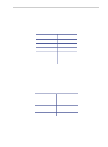
Table 1. ATA Operating Modes
Mode Specification
PIO 0 - 4
DMA 0 - 2
Ultra DMA 0 - 5
Table 2. Endurance Conditions
Condition Value
Power-On Hours 100%
Active/Idle 90%
Write Percentage 25%
Drive Capacity 16GB
File Transfer Size 64KB

PRELIMINARY/CONFIDENTIAL
Bad-Block Management
The bad-block mapping algorithm replaces bad blocks with new ones from available spares. Two
percent (2%) of the flash memory is held in reserve (spare block) for bad block replacement. Bad
blocks in the media are flagged when detected. The next time an attempt is made to access a flagged
block, it is immediately replaced by a spare block. The bad block mapping function enables data to
be automatically transferred from a bad sector to an available spare block.
The drive is scanned for bad blocks during the initialization of
the flash components. An initial bad bl ock table is created
from these identified marked bad blocks and any ba d b loc ks
discovered during the testing process.
Data Retention
Data stored on the SSD will remain valid for ten (10) years without requiring power support. The unit
can be stored under certain environmental conditions for extended periods without any occurrence
of data degradation. See Environmental Characteristics.
Error Detection and Correction
The Error Detection Code and Error Correcting Code (EDC/ECC) helps maintain data integrity by
allowing single or multiple bit corrections to the data stored in the flash array. If the data in the flash
array is corrupted due to aging or during the programming process, the EDC/ECC will compensate
for the errors to ensure the delivery of accurate data to the host computer. The EDC/ECC engine is
capable of correcting up to 4 bytes in error and detecting up to 5 bytes in error. An extensive retry
algorithm is also implemented on the SSD, so that single event disturbances such as ESD or EMF
occurring during a read operation can be readily overcome.
Reliability
The following factors affect the reliability statistics of the SSD:
• DC power is maintained as specified in this document
• Errors caused by the host are excluded from rates
• Errors from the same causes are counted as 1 block
• Data stream is assumed random
6 MACH2 2.5-Inch ATA Solid State Drive

PRELIMINARY/CONFIDENTIAL
Error Rates
Table 3 lists the error limit specifications. When all data correction mechanisms are enabled, the error
rate will be sustained through all operating temperature ranges as specified in the previous sections.
Table 3. Error Limits
Error Type Maximum Number of Errors
Recoverable Data Error 1 bit in 10
Unrecoverable Data Error Less than 1 bit in 10
20
20
Built-In Self Test (BIST)
The micro-controller tests the controller memory during power-up, and then performs a back-end
status check to verify proper flash memory controller operations. If a fault condition is detected in the
flash memory controller, the SSD’s status is reported as failed.
Mount Time
The amount of time required to initialize and mount a SSD varies according to the operating system
®
(Windows
, Linux®, etc.) environment and the storage capacity of the drive.
Seek Time
The SSD has no read/write heads or rotating platters. There is no seek time or rotational latency
issues. The SSD dramatically improves transaction throughput, particularly for applications that are
configured to take advantage of the characteristics of the drive.
Data Transfer Rates
The data transfer rate varies according to the flash controller/flash memory configuration of the drive.
The scalable architecture of the drive is capable of accommodating sustained and burst data transfer
rates as listed in Table 4.
Table 4. Data Transfer Rates
Parameter Value Units
Burst Transfer Rate 100 Megabytes/sec
Sustained Read Throughput 35 Megabytes/sec
Sustained Write Throughput 25 Megabytes/sec
MACH2 2.5-Inch ATA Solid State Drive 7

PRELIMINARY/CONFIDENTIAL
Repairs
A defective SSD should be replaced. There are no parts, assemblies or subassemblies that can be
repaired by the user. Please see the section titled Certification and Warranty on the inside of the
back cover page. Unauthorized repairs to the SSD will void the warranty.
Preventative Maintenance
No preventative maintenance is required. The SSD unit is sealed at the factory, and there are no
parts, assemblies, or subassemblies that require preventative maintenance on behalf of the user.
Please see the section titled Certification and Warranty on the inside of the back cover page.
Unauthorized maintenance to the SSD will void the warranty.
8 MACH2 2.5-Inch ATA Solid State Drive
PRELIMINARY/CONFIDENTIAL
ELECTRICAL SPECIFICATIONS
Power Requirements
The SSD requires a 5V power source. If a power failure occurs, the drive design ensures that the data
contained in the storage memory is preserved. Data loss or corruption does not occur.
Note: (1) The voltage rail, which includes ripples, does not exceed or fall below the voltage range as
specified by the Minimum and Maximum values, i.e., values are the absolute floor and ceiling for the
input voltages.
Power Consumption
The amount of power consumed by a SSD is determined by the storage (memory) capacity of the
drive, and the flash controller/memory configuration of the drive. See Table 6.
MACH2 2.5-Inch ATA Solid State Drive 9
Table 5. SSD Power Requirements
Item Requirement
1
Input Voltage
Minimum Voltage 4.75V
Maximum Voltage 5.25V
Ripple (0-30MHz) 70 mV p-p (for 3.3V)
Supply Rise Time 7 - 100 ms
Supply Fall Time < 5s
5V +/-5%
Table 6. SSD Typical Power Consumption
Operation Power Consumption
Standby 0.1W
Idle 0.3W
Read (35MB/sec) TBDW
Write (25MB/sec) TBDW
Purge TBDW
PRELIMINARY/CONFIDENTIAL
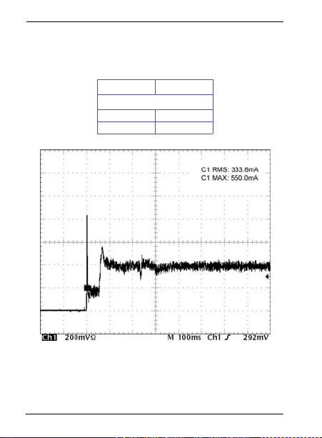
Start-Up Time and Current Draw
The Start-Up current is measured during the power-on phase of the computer and drive. See Table
7 and Figure 2.
Table 7. Start-Up Time and Current Draw
Start-Up Time ~850mS
Current Draw
Average RMS
Maximum Peak
333.6mA
550.0mA
Activity LED
Figure 2. Start-Up Current Draw
The SSD is configured to drive Pin 39 (-DASP; Disk Present/Secondary Active) of the ATA cable
during all command activity and during periods when the drive indicates a busy state. (Example: Offline diagnostic activities.)
10 MACH2 2.5-Inch ATA Solid State Dri ve

PRELIMINARY/CONFIDENTIAL
Power-On Ready Time
The Power-On Ready Time is less than 2.5 seconds. Power-On Ready Time is measured from the
time the drive is powered on to the time the drive is ready to accept the first command from the host.
Power Savings Commands
The drive will comply with all specifications that define the behavior of storage devices as it relates
to power management and Advanced Power Management (APM). When the SSD receives a power
management command, all data in the Write cache buffer is written to the media before Drive Ready
is asserted. The SSD supports the following Power Savings commands and respond with the
appropriate status:
Check Power Mode Standby Immediate
Idle Sleep
Standby
Power Mode at Power On
The drive will comply with the ATA-6 Power Management Specification. During the Power On Reset
sequence, the drive functions properly and responds as appropriate. In addition, if a SRST (ATA
Interface Reset) occurs during this sequence, the drive will still respond normally. After power on or
hard reset, the drive enters IDLE or STANDBY mode, depending on the setting by the host.
Grounding
Signal and chassis grounds are connected together in the drive. To ensure minimal EM emissions,
the user should provide maximum surface contact area when connecting the drive to the chassis
ground.
MACH2 2.5-Inch ATA Solid State Drive 11

PRELIMINARY/CONFIDENTIAL
INTERFACE SPECIFICATIONS
SSD Operation
The SSD is comprised of three primary functional blocks: the ATA (IDE) interface connector, SSD
controller and NAND flash memory. Read/write data transfer requests are initiated by the host via the
ATA (IDE) bus interface. Once received, the controller, under the direction of the microcontroller,
processes the request.
Commands that do not require data to be read from or written to the flash memory controller are
typically handled by the controller. Some commands may require the controller to use external
circuitry that do not involve the flash memory controller.
Write Operations
When a write operation is requested and data is received, the controller uses integrated DMA
controllers to transfer the data from host memory to the flash memory controller. Through a standard
ATA (IDE) interface, the flash memory controller transfers the data from the controller to available
locations in the local flash memory of the SSD. The controller notifies the host after the write
operation is completed.
Read Requests
If a read request is received, the controller retrieves the data from the local flash memory via the flash
memory controller. If the controller is responding to a PIO read operation, it presents the data to the
ATA bus. If it is responding to a UDMA read request, the controller writes the data directly to system
memory on the host. Regardless of the type of operation (PIO or UDMA), the controller notifies the
host when the data is ready for transmission.
12 MACH2 2.5-Inch ATA Solid State Dri ve
The microcontroller initiates and controls all activity within th e
controller, including bad-block mapping and executing the wearleveling algorithms.
The controller decodes an incoming host command, and
configures the appropriate interrupts and statu s for the local
microprocessor to handle various ATA commands. For read and
write transfer commands, the hardware can handle the initial
handshake with the host automatically. If firmware enab les full
auto mode, read and write transfers can be fully handled by
hardware with minimum firmware support.

PRELIMINARY/CONFIDENTIAL
Primary and Secondary Modes
The SSD supports Primary (Device 0) and Secondary (Device 1) modes:
Device Mode Description
Drive address at system ATA I/O address 1F0h - 1F7h and 3F6h - 3F7h. The
Primary
host must provide chip-enable #CS0 and #CS1. The SSD decodes addresses
DA0 - DA2.
Drive address at system ATA I/O address 170h - 177h and 376h - 377h. The
Secondary
host must provide chip-enable #CS0 and #CS1. The SSD decodes addresses
DA0 - DA2.
I/O Primary and Secondary ATA (IDE) Modes
Primary and secondary drive addressing modes allow hosts to use the reserved disk drive I/O
addresses as defined by the ATA specification. This provides system designers with the simplest way
to accommodate ATA-protocol devices.
Addressing Modes
The SSD, on a command-by-command basis, can operate in either CHS or LBA addressing modes.
Identify Device Information (See Identify Device Information) signals the host whether the drive
supports LBA mode. The host selects LBA mode via the Drive/Head Register. Sector Number,
Cylinder Low, Cylinder High, and Drive/Head register bits HS3=0 contain the zero-based LBA. The
sectors are linearly mapped with: LBA = 0 => Cylinder 0, Head 0, Sector 1. Regardless of the
translation mode, a sector LBA address does not change. LBA = (Cylinder * No of Heads + Head) *
(Sectors/Track) + (Sector - 1). Table 8 lists the supported IDE addressing modes.
Table 8. ATA (IDE) Bus Addressing Modes
#CS0 #CS1 DA2 DA1 DA0 #IORD - “0” #IOWR - “0”
1 1 X X X Hi-Z Not Used
1 0 0 X X Hi-Z Not Used
1 0 1 0 X Hi-Z Not Used
0 0 X X X Invalid Invalid
1 0 1 1 0 Alternate Status Device Control
1 0 1 1 1 Device Address Not Us ed
0 1 0 0 0 Data Data
0 1 0 0 1 Error Feature
0 1 0 1 0 Sector Count Sector Count
0 1 0 1 1 Sector Number Sector Number
0 1 1 0 0 Cylinder Low Cylinder Low
0 1 1 0 1 Cylinder High Cylinder High
0 1 1 1 0 Drive/Head Drive/Head
0 1 1 1 1 Status Command
MACH2 2.5-Inch ATA Solid State Drive 13

PRELIMINARY/CONFIDENTIAL
44-Pin ATA Bus Connector
The SSD is equipped with a 44-pin ATA bus connector. See Figure 3. DC power and IDE bus traffic
is supplied through a non-shielded 44-conductor I/O cable.
14 MACH2 2.5-Inch ATA Solid State Dri ve
The SSD has a plastic key to block pin 20 on the ATA bus
(IDE) interface connector. This prevents possible damag e to
the SSD by making an improper connection impossible.
ATA standards require 80-conductor cables to be used for
Ultra DMA (UDMA) Modes 3 through 5.
The length of the non-shielded cable should not exceed
457.2mm (18 inches).
Figure 3. 44-pin ATA (IDE) Bus Connector
PRELIMINARY/CONFIDENTIAL
Connector Pinout Signals
Table 9 provides the signal assignment for each pin on the ATA (IDE) bus connector. The table
applies to the 44-pin ATA bus/DC power combination connector used on 2.5-inch drives.
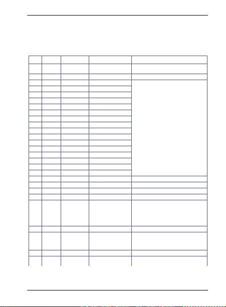
Pin Pin Type Signal Symbol Signal Name Signal Description
1 1 -RESET HOST RESET Reset signal from host. Reset is active on power up
2 Ground GND - Ground
3 I/O D07 HOST DATA 07 Pins 3 through 18 (16 lines (15-0) ca rry the data
4 I/O D08 HOST DATA 08
5 I/O D06 HOST DATA 06
6 I/O D09 HOST DATA 09
7 I/O D05 HOST DATA 05
8 I/O D10 HOST DATA 10
9 I/O D04 HOST DATA 04
10 I/O D11 HOST DATA 11
11 I/O D03 HOST DATA 03
12 I/O D12 HOST DATA 12
13 I/O D02 HOST DATA 02
14 I/O D13 HOST DATA 13
15 I/O D01 HOST DATA 01
16 I/O D14 HOST DATA 14
17 I/O D00 HOST DATA 00
18 I/O D15 HOST DATA 15
19 Ground GND - Ground
20 - - - No connection. Reserved for connector key.
21 O DREQ DMA REQUEST Not used.
22 Ground GND - Ground
23 I -IOWR I/O WRITE This I/O Write strobe pulse is used to clock I/O data
24 Ground GND - Ground
25 I -IORD I/O READ This is a Read strobe gen erated by the host. Th e
26 Ground GND - Ground
27 I IORDY I/O READY Not used. Pulled up to Vcc through a 4.7k oh m
MACH2 2.5-Inch ATA Solid State Drive 15
Table 9. ATA Connector Pinout Configuration
and inactive thereafter.
between the controller and the host. The low 8 lines
transfer commands and the ECC information
between the host and the controller.
or commands on the drive data bus into the drive
controller registers when the drive is configured to
use the I/O interface. The clocking will occur on the
negative to positive edge of the signal (trailing
edge.
signal gates I/O data or status on the host bus and
strobes the data from the controller into the host on
the low to high transition (trailing edge).
resistor.

PRELIMINARY/CONFIDENTIAL
Pin Pin Type Signal Symbol Signal Name Signal Description
28 I -CSEL CABLE SELECT This internally pulled up signal is used to configure
29 I -DACK DMA ACKNOWLEDGE Not used.
30 Ground GND - Ground
31 O INTRQ INTERRUPT REQUEST This is an interrupt request from the controller to the
32 O -IOS16 I/O SELECT 16 Not used.
33 I A1 HOST ADDRESS 1 The addres s line A1 is used to select one of eight
34 I/O -PDIAG After an Executive diagnostic command to indicate
35 I A0 HOST ADDRESS 0 The address lines A0 and A2 are used to select one
36 I A2 HOST ADDRESS 2
37 I -CS1 HOST CHIP SELECT 1 The chip select signal used to select the Task F ile
38 I -CS2 HOST CHIP SELECT 2 The chip select signal used to select the Alternate
39 I/O -DASP DISK ACTIVE/
40 Ground GND - Ground
41 - V
42 - V
43 Ground GND - Ground
44 - - - No Connection
SECONDARY PRESENT
Supply Voltage 5V Power Supply
CC
Supply Voltage 5V Power Supply
CC
the drives as the Primary or the Secondary device.
When the pin is grounded, the device is configured
as the Primary device. When the pin is open, the
device is configured as a Secondary device.
host, asking for service. This signal is the acti ve
high Interrupt Request to the host.
registers in the controller Task File.
that the Primary device has passed its diagnostics,
this bi-directional open drain signa l is asserte d by
the Secondary device.
of eight registers in the controller Task File.
register.
Status register and the Device Control register.
This input/output is the Disk Active/Secondary
Present signal in the Primary/Secondary
handshake protocol.
16 MACH2 2.5-Inch ATA Solid State Dri ve

PRELIMINARY/CONFIDENTIAL
ATA COMMANDS
Overview
This section provides information on the ATA commands supported by the SSD. The commands are
issued to the ATA by loading the required registers in the command block with the supplied
parameter, and then writing the command code to the register.
Standard ATA Commands
Table 10 lists each command along with its respective command code and registers accessed by the
command. For detailed descriptions of the ATA commands, refer to the ATA-6 specification.
Command
CHECK POWER MODE 98h or E5h No Yes No No
DOWNLOAD MICROCODE 92h Yes No No No No
ERASE SECTOR C0h No Yes Yes Yes
EXECUTE DRIVE DIAGNOSTIC 90h No No No No
FLUSH CACHE E7h TBD TBD TBD TBD TBD
FLUSH CACHE EXTENDED EAh TBD TBD TBD TBD TBD
FORMAT TRACK 50h No Yes No Yes
IDENTIFY DEVICE ECh Yes No No No
IDLE 97h, E3h No Y No No
IDLE IMMEDIATE 95h, E1h No No No No
INITIALIZE DRIVE PARAMETERS 91h No Yes No No
NOP 00h No No No No
READ BUFFER E4h No No No No No
READ DMA C8h No Yes Yes Yes
READ DMA EXTENDED 25h No Yes Yes Yes
READ DMA QUEUED C7h No Yes Yes Yes
READ DMA QUEUED EXT 26h No Yes Yes Yes
READ MULTIPLE C4h No Yes Yes Yes
READ MULTIPLE EXTENDED 29h No Yes Yes Yes
READ SECTOR(S) 20h No Yes Yes Yes
READ SECTOR(S) EXTENDED 24h No Yes Yes Yes
READ VERIFY SECTOR(S) 40h No Yes Yes Yes
READ VERIFY EXTENDED 42h No Yes Yes Yes
MACH2 2.5-Inch ATA Solid State Drive 17
Table 10. Supported ATA Commands
Feature
Register
Sector
Count
Register
Command
Code (Hex)
Sector
Number
Register
Cylinder
High/Low
Register
Drive/Head
Number
Register
Yes
Yes
Yes
Yes
Yes
Yes
Yes
Yes
Yes
Yes
Yes
Yes
Yes
Yes
Yes
Yes
Yes
Yes
Yes
(a)
(a)
(a)
(b)
(a)
(a)
(a)
(b)
(b)
(b)
(b)
(b)
(b)
(b)
(b)
(b)
(b)
(b)
(b)

PRELIMINARY/CONFIDENTIAL
Sector
Sector
Cylinder
Command
Command
RECALIBRATE 10h No No No No
SECURITY DISABLE PASSWORD F6h No No No No
SECURITY ERASE PREPARE F3h No No No No
SECURITY ERASE UNIT F4h No No No No
SECURITY FREEZE LOCK F5h No No No No
SECURITY SET PASSWORD F1h No No No No
SECURITY UNLOCK F2h No No No No
SEEK 70h - 7Fh No No Yes Yes
SET FEATURES EFh No Yes Yes Yes
SET MULTIPLE MODE C6h No Yes No No
SLEEP E6h No No No No
SMART B0h Yes Yes Yes Yes
STANDBY 96h or E2h No Yes No No
STANDBY IMMEDIATE 94h or E0h No No No No
WRITE BUFFER E8h No Yes Yes Yes
WRITE DMA CAh No Yes Yes Yes
WRITE DMA EXTENDED 35h No Yes Yes Yes
WRITE DMA QUEUED CCh No Yes Yes Yes
WRITE DMA QUEUED EXT 36h No Yes Yes Yes
WRITE MULTIPLE C5h No Yes Yes Yes
WRITE MULTIPLE EXTENDED 39h No Yes Yes Yes
WRITE MULTIPLE FUA EXT CEh No Yes Yes Yes
WRITE SECTOR(S) 30h No Yes Yes Yes
WRITE SECTOR(S) EXTENDED 34h No Yes Yes Yes
Code (Hex)
Feature
Register
Count
Register
Number
Register
High/Low
Register
Drive/Head
Number
Register
Yes
Yes
Yes
Yes
Yes
Yes
Yes
Yes
Yes
Yes
Yes
Yes
Yes
Yes
Yes
Yes
Yes
Yes
Yes
Yes
Yes
Yes
Yes
Yes
Notes:
(a) Only drive parameters are valid.
(b) Drive and head parameters are valid.
(c) Address to Drive 0 (zero). When executed, both drives (Primary and Secondary)
execute this command.
18 MACH2 2.5-Inch ATA Solid State Dri ve
(a)
(a)
(a)
(a)
(a)
(a)
(a)
(b)
(b)
(a)
(a)
(b)
(a)
(a)
(b)
(b)
(b)
(b)
(b)
(b)
(b)
(b)
(b)
(b)

PRELIMINARY/CONFIDENTIAL
Standard ATA Command Summary
Table 11 provides a summary of each supported ATA command.
Command Hex Value Description
CHECK POWER MODE 98h, E5h The Check Power Mode command allows the host to determ ine
DOWNLOAD MICROCODE 92h The command allows the host to alt er the microcode of the
ERASE SECTOR C0h This command w ill pre-erase and c ondition the data sectors in
EXECUTE DRIVE DIAGNOSTIC 90h This command performs the internal diagnostic tests
FLUSH CACHE E7h This command is used by the host to request the device to flush
FLUSH CACHE EXTENDED EAh This command is used by the ho st to request the device to flush
FORMAT TRACK 50h This command writes the desired head and cylinder of the
IDENTIFY DEVICE ECh This command allows the host to receive parameter information
IDLE 97h, E3h This command will cause the drive to set BSY, enter the IDLE
MACH2 2.5-Inch ATA Solid State Drive 19
Table 11. ATA Command Summary
the current power mode of the device. The C heck Power Mo de
command shall not cause the device to change po wer or affect
the operation of the Standby timer.
device. The data transferred using the Dow nload Microcode
command is vendor-specific. All transfers are an inte ger mult iple
of the sector size. The size of the data transfer is determined by
the contents of the LBA Low register and the Sector Count
register. The LBA Low register will extend the Se ctor Count
register to create a 16-bit sector count value. The LBA Low
register will be the most significant eight bits and the Sector Count
register will be the least significant eight bits. A value of zero in
the LBA Low and Sector Count registers specify that no data is to
be transferred. This allows transfer sizes from 0 bytes to
33,553,920 bytes, in 512-byte increments. The Features register
will determine the effect of the Download Microcode command.
advance.
implemented by the controller.
the Write cache. If there is data in the Write cache, that data shall
be written to the media. The command will not indicate
completion until the data is flushed to t he media or an error
occurs. If the device supports more tha n 28 bits of addre ssing,
this command shall attempt to flush all the data in the cache. If the
Write cache is disabled or is not p res en t, th e device will indicate
completion without er ror . Th e com mand is ma ndat or y for de vic es
not implementing the PACKET feature set.
the Write cache. If there is data in the Write cache, that data shall
be written to the media. The command will not indicate
completion until the data is flushed to t he media or an error
occurs. If the Write cache is disabled or is not present, the device
will indicate completion without error. This command is
mandatory for devices that implement the 48-bit Address feat ure
set.
selected drive with a vendor-unique data pattern (typically 00h or
FFh). The drive accepts a sector buffer of data from the host to
follow the command with the same protocol as the Write Sector(s)
- 30h command, although the information in the cach e is not
used.
from the drive.
mode, clear BSY, and generate an interrupt. If the sector count is
zero, the automatic power down mode is disabled.

PRELIMINARY/CONFIDENTIAL
IDLE IMMEDIATE 95h, E1h This command will cause the driv e to set BSY, enter th e IDLE
INITIALIZE DRIVE PARAMETERS 91h This command will enable the host to set the num ber o f sect ors
NOP 00h This command is mandatory for devices that implement the
READ BUFFER E4h This command is optional for devices tha t do not implem ent the
READ DMA C8h This comman d is mandato ry for devices that do no t implement
READ DMA EXT 25h This command is mandatory for devices that implement the 48-bit
READ DMA QUEUED C7h This command is mandatory for devices that implement the TCQ
READ DMA QUEUED EXT 26h This command is mandatory for devices that implement the TCQ
READ MULTIPLE C4h This command is similar to the Read S ector(s) - 20h command.
READ MULTIPLE EXTENDED 29h This command is mandatory for all devices that impleme nt the
READ SECTOR(S) 20h This command will read from 1 to 256 sectors as specified in the
READ SECTOR(S) EXTENDED 24h This command is mandatory for devices that implement the 48-bit
READ/VERIFY SECTOR(S) 40h This command will verify one or more sectors by transferring data
(READ) mode, clear BSY, and generate an interrupt.
per track and the number of heads per cylinder.
PACKET and TCQ feature sets. The device will re spond with
command aborted. For devices that imple ment the TC Q feature
set, the subcommand 00h in the Featur e field shall abort any
outstanding queue. Subcommand codes 01h through FFh in the
Feature field shall not affect the status of any outstanding queue.
PACKET feature set. The command wil l enable the ho st to re ad
a 512-byte block of data . The Writ e Buf fer ( E8h) c ommand shou ld
precede the Read Buffer (E4h) com man d, les t th e d ata re turn ed
be indeterminate.
the PACKET feature set. The command will allow the host to read
data using the DMA data transfer protocol.
Address feature set. The command will allow the host to read
data using the DMA data transfer protocol.
feature set. The command is similar in function to the Read DMA
(C8h) command. The device may releas e or execute the data
transfer without performing a release if the data is ready to
transfer.
and 48-bit feature sets. The command is similar in function to the
Read DMA (C8h) command. The device may release or execute
the data transfer with ou t per f o rm ing a re l e as e if th e da t a i s re ad y
to transfer.
Interrupts are not generated on each sector, but on the transfer of
a block that contains the number of sectors as de fined by a Set
Multiple Mode - C6h command.
48-bit Address feature set. The command will read the number of
logical sectors specified in the Count field. The number of logical
sectors determines the DRQ data block count, which in turn will
determine the number of logical sectors that are to be transferred.
Sector Count Register. A sector count of 0 (zero) request s 256
sectors. The transfer will begin at the s ector specified in the
Sector Number Register.
Address feature set. This comman d will read from 1 to 256 to
65,536 logical sectors as specified in the S ect or C oun t Re gis ter.
A sector count of 0 (zero) will request 65,536 logical sectors. The
transfer will begin at the sector specified in the LBA field.
from the flash media to th e dat a buf fer and v erif yin g tha t th e ECC
is correct. The command is identical to t he Rea d S ect or(s) - 20h
command, except that DRQ is never set and no data is
transferred to the host.
20 MACH2 2.5-Inch ATA Solid State Dri ve

PRELIMINARY/CONFIDENTIAL
READ/VERIFY EXTENDED 42h This command is mandatory for devices that implement the 48-bit
RECALIBRATE 10h The SSD performs only the interface timing and register
SECURITY DISABLE PASSWORD F6h This command is ma ndatory for devices that implement the
SECURITY ERASE PREPARE F3h This command is mandatory for devices that implement the
SECURITY ERASE UNIT F4h This command is ma ndatory for devices that implement the
SECURITY FREEZE LOCK F5h This command is mandatory for devices tha t implement the
SECURITY SET PASSWORD F1h This command is mandatory for dev ices that implement the
SECURITY UNLOCK F2h This command is mandatory for devices that implement the
Address feature set. The command is i dentical to the Read
Sector(s) Extended (24) command, except that no data is
transferred from the device to the host. The d evice will read the
data stored in the media and verify that no errors exist.
operations. When th is co mmand is i ssued , the S SD se ts BS Y and
waits for an appropriate length of time, after which it clears B SY
and issues an interrupt. When this command ends normally, the
SSD is initialized.
Security Mode feature set. The com ma nd will tra nsf er 5 12 by tes
of predefined data from the host. If the p assword selected by
Word 0 matches the password th at wa s pre viou sly sa ved b y the
device, the device shall disable Lock mode. The co mmand will
not change the Master password. T he Master password is
reactivated when a User password is set. The command will only
complete successfully if the device is in Unlocked mode.
Security Mode feature set. The comm and i s issu ed im media tely
before the Security Erase Unit (F4h) command to en able dev ice
erasing and unlocking. The command prevents accidental loss of
data on the device.
Security Mode feature set. The com ma nd will tra nsf er 5 12 by tes
of predefined data from th e h os t . If th e pa s sw o rd do es no t mat c h
the password previously saved by the device, the device shall
reject the command and abort it. W he n a N orm al Erase mode is
specified, the Security Erase Unit command shall write bin ary
zeros to all user data areas. If the optional Enhanced Erase mode
is specified, the device shall write predetermined data patterns to
all user data areas; the current d ata is overwritten, including
sectors that are no longer in use due to reallocation.
Security Mode feature set. The c om man d sha ll set th e device to
Frozen mode. Other commands that upd ate the device Lock
mode are aborted. Frozen mode can be disabled by a power -off
or hardware reset. If the command is issued while the device is in
Frozen mode, the command is ex ecuted and the device will
remain in Frozen mode.
Security Mode feature set. The com ma nd will tra nsf er 5 12 by tes
of predefined data from the host. The data controls the function of
this command, which in turn defines the intera ction of the
identifier and security level bits. The user can in tu rn set the
Master or User passwords, and the security level of the device.
Security Mode feature set. The com ma nd will tra nsf er 5 12 by tes
of predefined data from the host. The data controls the function of
this command, which in turn defines the intera ction of the
Identifier bit. If the Identifier bit is set to Master and the current
security level is high, the password is com pared with the stored
Master password. If the device is in maximum security level then
the unlock shall be rejected. If the Identifier bit is set to User, then
the device shall compare the supplied password with the stored
User password. If the password comparison fails, the device shall
abort the command and report a decrea se in the incremental
value in the unlock counter.
MACH2 2.5-Inch ATA Solid State Drive 21

PRELIMINARY/CONFIDENTIAL
SEEK 70h, 7Fh This command is effectively a NOP command to the SSD
SET FEATURES E Fh This command is used by the host to establish or select cert ain
SET MULTIPLE MODE C6h This comman d enables the SSD to p erform multiple read and
SET SLEEP MODE 99h, E6h This is the only command that allows the host to configure the
SLEEP E6h This command is mandatory for devices that implement the
SMART B0h See S.M.A.R.T. Support.
STANDBY 96h, E2h This command will config ure the drive for Standby Mode. If the
STANDBY IMMEDIATE 94h, E0h This command will cause the SSD to set BYS, enter the Standby
WRITE BUFFER E8h This command is optional for devices that implement the General
WRITE DMA CAh This command is ma ndatory for devices that implement the
WRITE DMA EXT 35h This command is mandatory for devices that implement the 48-bit
WRITE DMA FUA EXT 3Dh This command is mandatory for devices that implement the 48-bit
although it does perform a range check.
features supported by the drive. When the SSD receives this
command, it sets BSY, checks the contents of th e Features
register, applies changes as necessary, clears BSY and
generates an interrupt. If the valu e in the register does not
represent a feature supported by the drive, the command is
canceled with the Abort Error condition.
write operations and establishes the block cou nt for these
commands.
drive for Sleep Mode. When the driv e is set t o Sleep M ode, the
SSD clears the BSY line and issues an interrupt. The card enters
Sleep Mode and the hardware or software must be reset to
activate the drive.
Power Management feature set. The co mmand will cause the
device to enter Sleep mode. The dev ice will not power-on in
Sleep mode nor remain in Sleep mode following a reset
sequence. The method used to dea ctivate Sleep mode is
transport specific. The Power Management feature set is
mandatory for devices that do not im plement the PACKET
Command set. This command is mandatory when power
management is not implemented b y the PA CK ET Command set
device.
Sector Count Register is a value other than 0H, an Auto Power
Down is enabled and when the dri ve returns to Idle M ode, the
timer starts a countdown. The time is set in the Sector Count
Register.
Mode, clear BSY, and return the interrupt immediately.
feature set. This command allows the hos t to write th e contents
of one 512-byte block of data in the in the buffer of the device.
General feature set. The command allo ws the host to write d ata
using the DMA data transfer protocol.
Address feature set. The comman d allo ws th e h ost to write data
using the DMA data transfer protocol.
Address feature set. The command provides the same function
as Write DMA Extended (35h) regardles s of whether write
caching is enabled. The user data is written to the me dia bef ore
ending status for the command is reported.
22 MACH2 2.5-Inch ATA Solid State Dri ve

PRELIMINARY/CONFIDENTIAL
WRITE DMA QUEUED CCh This command is mandatory for devices that implement the TCQ
WRITE DMA QUEUED EXT 38h This command is mandatory for devices that implement the TCQ
WRITE DMA QUEUED FUA EXT 3Eh This command is mandatory for devices that implement the TCQ
WRITE MULTIPLE C5h This comma nd is simila r to the Wri te Sector(s ) - 30h com mand.
WRITE MULTIPLE EXT 39h This command is mandatory for devices that implement the 48-bit
WRITE MULTIPLE FUA EXT CEh This command is mandatory for devices that implement the 48-bit
WRITE SECTOR(S) 30h This command will write from 1 to 256 sectors as specified in the
WRITE SECTOR(S) EXT 34h This command is mandatory for devices that implement the 48-bit
feature set. The command is similar to the Write DMA (CAh)
command. The device may perform a release or may execute the
data transfer without performing a rele ase if the da ta is re ady to
transfer. If the device performs a release, the host should reselect
the device using the SERVICE command. Once the data transfer
has begun, the device shall not perform a release until the entire
data transfer is complete.
and 48-bit Address feature sets. The command is similar to Write
DMA Extended (35h). The device may perform a release or may
execute the data transfer without performing a release if the data
is ready to transfer. If the device performs a release, the host
should reselect the device using the SERVI CE comma nd. On ce
the data transfer has begun, the device shall not perform a
release until the entire data transfer is complete.
and 48-bit Address feature sets. The comm and is similar to the
Write DMA Extended (35h) command. The device may perform a
release or may execute the dat a transfer without per forming a
release if the data is ready to transfer. If the device performs a
release, the host should reselect the device using th e SERVI CE
command. The device does not perform a release onc e the data
transfer has begun and has been completed.
Interrupts are not presented on each sector, but on the transfer of
a block which contains the number of se cto rs d efin ed by the Set
Multiple Mode - C6h command.
Address feature set. The command will write the number of
logical sectors specified in the Count field. The command is
similar to Write Sector(s) (30h). Interrupts are not presen ted on
each sector, but on the transfer of blocks that contain the number
of sectors defined by LBA mode.
Address feature set. The command has the same functionality of
Write Multiple Ext (39h), except tha t regar dless of whe ther w rite
caching is enabled, the user data is written to the media bef ore
the ending status of the command is reported.
Sector Count Register. A sector count of 0 (zero) will request 256
sectors. The transfer begins at the se ctor sp ecif ied in t he Sec tor
Number Register.
Address feature set. The command will write 1 to 6 5,536 logical
sectors as specified in the Sector Count Register. A sector count
value of 0 will request 65,536 logical sectors.
MACH2 2.5-Inch ATA Solid State Drive 23

PRELIMINARY/CONFIDENTIAL
S.M.A.R.T. Support
S.M.A.R.T. is an acronym for Self-Monitoring, Analysis and Reporting Technology. The S.M.A.R.T.
feature set protects the user from unscheduled downtime by monitoring and storing critical drive
performance and calibration parameters. A S.M.A.R.T. feature set device attempts to predict the
occurrence of near-term degradation or fault conditions. The host system is warned of a negative
reliability condition, which in turn warns the user of the impending risk of data loss. The user can then
take appropriate action to minimize the risk.
Support for the S.M.A.R.T. feature set is indicated by the Identify Device (ECh) command:
Word 82 Bit 0 The S.M.A.R.T. feature set is supported. This information is set during the drive
Word 85 Bit 0 The S.M.A.R.T. feature set has been enabled via the SMART ENABLE
initialization sequence.
OPERATIONS command. The information is dynamic; the SMART ENABLE
OPERATIONS command and SMART DISABLE OPERATIONS command are
invoked. The most current setting must be reflected in the output of the IDENTIFY
DEVICE command. S.M.A.R.T. operations are enabled by default.
S.M.A.R.T. Commands
Table 12 lists the commands that are identified by the value placed in the Feature register.
Table 12. S.M.A.R.T. Command Values
Value Command Note
00h-CFh Reserved RSVD
D0h SMART READ DATA Optional
D1h Obsolete OBS
D2h SMART ENABLE/DISABLE ATTRIBUTE AUTOSAVE Mandatory
D3h Obsolete OBS
D4h SMART EXECUTE OFF-LINE IMMEDIATE Optional
D5h SMART READ LOG Optional
D6h SMART WRITE LOG Optional
D7h Obsolete OBS
D8h SMART ENABLE OPERATIONS Mandatory
D9h SMART DISABLE OPERATIONS Mandatory
DAh SMART RETURN STATUS Mandatory
DBh Obsolete OBS
DCh-DFh Reserved RSVD
E0h-FFh Vendor-Specific VSC
24 MACH2 2.5-Inch ATA Solid State Dri ve

PRELIMINARY/CONFIDENTIAL
S.M.A.R.T. Attributes
Table 13 lists the S.M.A.R.T. attributes that are supported.
Table 13. Supported S.M.A.R.T. Attributes
ID Name Description
1 Raw Read Error Frequency of errors while reading raw data from a disk.
9 Power-On Hours Number of hours elapsed in the Power-On state.
12 Power Cycle Number of Power-On events.
187 Reported Uncorrectable Errors The number of uncorrectable errors reported at the interface.
194 Temperature Temperature of base casting. (Requires integrated
195 ECC On-the-Fly Number of ECC on-the-fly errors.
196 Offline Reallocation Event Total number of sectors remapped.
197 Pending Defects Number of sectors currently suspected in need of remapping.
198 Offline Surface Scan Number of uncorrected errors that occurred during offline
199 UDMA CRC Error (PATA Only) Number of CRC errors during UDMA mode.
temperature sensor.)
scan.
Identify Device Information
The Identify Device command enables the host to receive parameter information from the SSD.
When the Identify Device command executes, the SSD sets the BSY bit, prepares to transfer the 256
words of SSD identification data to the host, sets the DRQ bit, clears the BSY bit, and then generates
an interrupt. The host can then transfer the data by reading the Data register. All reserved bits or
words are all zero. Table 14 contains typical Identify Device Information for the SSD.
Identify Device Information Key
F Content of the word is Fixed and does not change. For removable medi a devices, thes e value
may change when the media is removed or changed.
V Content of the w ord is Variable and may change depending on the state of the device or the
commands executed by the device.
X Content of the word is Vendor-Specific and may be fixed or variable.
R Content of the word is Reserved and shall be 0 (zero).
MACH2 2.5-Inch ATA Solid State Drive 25

PRELIMINARY/CONFIDENTIAL
Table 14. Identify Device Information
Word F/V/X/R Description
0 General configuration bit-significant information
F15 0 = ATA Device
X 14:8 Retired
F 7 1 = Removable Media Device
X6 Obsolete
X5:3Retired
V 2 Response Incomplete
X1 Retired
F0 Reserved
1VObsolete
2 V Specific Configuration
3XObsolete
4 -5 X Retired
6XObsolete
7 - 8 V Reserved for assignment by the CompactFlash™ Association
9XRetired
10 - 19 F Serial Number (20 ASCII Characters)
20 - 21 X Retired
22 X Obsolete
23 - 26 F Firmware Revision (8 ASCII Characters)
27 - 46 F Model Number (40 ASCII Characters)
47 F 15:8 80h
F 7:0 00h = Reserved
F 01h - FFh = Maximum number of sectors that shall be transferred per
48 F Reserved
49 Capabilities
F 15:14 Reserved for IDENTIFY PACKET DEVICE Command
F 13 1 = Standby timer values as specified in this standard are supported
F 12 Reserved for IDENTIFY PACKET DEVICE Command
F 11 1 = IORDY supported
26 MACH2 2.5-Inch ATA Solid State Dri ve
interrupt on READ/WRITE MULTIPLE Commands
0 = Standby timer values shall be managed by the device

PRELIMINARY/CONFIDENTIAL
F 10 1 = IORDY may be disabled
F 9 1 = LBA supported
F 8 1 = DMA supported
X7:0Retired
50 Capabilities
F 15 Shall be cleared to zero
F 14 Shall be set to one
F13 :2Reserved
X1 Obsolete
F 0 Shall be set to one to indicate a device-specific Standby Timer Value
51 - 52 X Obsolete
53 F 15:3 Reserved
F 2 1 = The fields reported in Word 88 are valid
F 1 1 = The fields reported in Words 70:64 are valid
X0 Obsolete
54 - 58 X Obsolete
59 F 15:9 Reserved
V 8 1 = Multiple Sector Setting is Valid
V 7:0 xxh = Current setting for number of sectors that shall be transferred per
60 - 61 F Total Number of User-Addressable Sectors
62 X Obsolete
63 F 15:11 Reserved
V 10 1 = Multiword DMA Mode 2 is selected
V 9 1 = Multiword DMA Mode 1 is selected
V 8 1 = Multiword DMA Mode 0 is selected
F7:3Reserved
F 2 1 = Multiword DMA Mode 2 and below are supported
MACH2 2.5-Inch ATA Solid State Drive 27
0 = IORDY may be supported
minimum
0 = The fields reported in Word 88 are invalid
0 = The fields reported in Words 70:64 are invalid
interrupt on R/W MULTIPLE Command
0 = Multiword DMA Mode 2 is not selected
0 = Multiword DMA Mode 1 is not selected
0 = Multiword DMA Mode 0 is not selected

PRELIMINARY/CONFIDENTIAL
F 1 1 = Multiword DMA Mode 1 and below are supported
F 0 1 = Multiword DMA Mode 0 is supported
64 F 15:8 Reserved
F 7:0 PIO Modes supported
65 Minimum Multiword DMA Transfer Cycle Per Word
F 15:0 Cycle Time in Nanoseconds
66 Manufacturer’s Recommended Multi-word DMA Transfer Cycle
F 15:0 Cycle Time in Nanoseconds
67 Minimum PIO Transfer Cycle Time without Flow Control
F 15:0 Cycle Time in Nanoseconds
68 Minimum PIO Transfer Cycle Time with IORDY Flow Control
F 15:0 Cycle Time in Nanoseconds
69 - 70 F Reserved (For Future Command Overlap and Queuing)
71 - 74 F Reserved for IDENTIFY PACKET DEVICE Command
75 Queue Depth
F 15:5 Reserved
F 4:0 Maximum Queue Depth - 1
76 - 79 F Reserved
80 F Major Version Number
28 MACH2 2.5-Inch ATA Solid State Dri ve
0000h or FFFFh = Device does not report version
F 15 Reserved
F 14 Reserved for ATA/ATAPI-14
F 13 Reserved for ATA/ATAPI-13
F 12 Reserved for ATA/ATAPI-12
F 11 Reserved for ATA/ATAPI-11
F 10 Reserved for ATA/ATAPI-10
F 9 Reserved for ATA/ATAPI-9
F 8 Reserved for ATA/ATAPI-8
F 7 Reserved for ATA/ATAPI-7
F 6 1 = Supports ATA/ATAPI-6
F 5 1 = Supports ATA/ATAPI-5
F 4 1 = Supports ATA/ATAPI-4
F 3 1 = Supports ATA-3
X2 Obsolete

PRELIMINARY/CONFIDENTIAL
X1 Obsolete
F0 Reserved
81 F Minor Version Number
82 Command Set Supported
83 Command Sets Supported
MACH2 2.5-Inch ATA Solid State Drive 29
0000h or FFFFh = Device does not report version
0001h-FFFFh = Revision of ATA Standard guiding minor version number
implementation
X 15 Obsolete
F 14 1 = NOP Command supported
F 13 1 = READ BUFFER Command supported
F 12 1 = WRITE BUFFER Command supported
X 11 Obsolete
F 10 1 = Host Protected Area Feature Set supported
F 9 1 = DEVICE RESET Command supported
F 8 1 = SERVICE Interrupt supported
F 7 1= RELEASE Interrupt supported
F 6 1 = Look Ahead supported
F 5 1 = Write Cache supported
F 4 Shall be cleared to zero to indicate that the PACKET Command feature
F 3 1 = Power Management Feature Set supported (mandatory)
F 2 1 = Removable Media Feature Set supported
F 1 1 = Security Mode Feature Set supported
F 0 1 = SMART Feature Set supported
F 15 Shall be cleared to zero
F 14 Shall be set to one
F 13 1 = FLUSH CACHE EXT Command supported
F 12 1 = FLUSH CACHE Command supported (mandatory)
F 11 1 = Device Configuration Overlay feature set supported
F 10 1 = 48-Bit Address feature set supported
F 9 1 = Automatic Acoustic Management feature set supported
F 8 1 = SET MAX security extension supported
F 7 See Address Offset Reserved Area Boot, INCITS TR27:2001
F 6 1 = SET FEATURES subcommand required to spin-up after power-up
set is not supported

PRELIMINARY/CONFIDENTIAL
F 5 1 = Power-Up in Standby feature set supported
F 4 1 = Removable Media Status Notification feature set supported
F 3 1 = Advanced Power Management feature set supported
F 2 1 = CFA feature set supported
F 1 1 = READ/WRITE DMA QUEUED supported
F 0 1 = DOWNLOAD MICROCODE Command supported
84 Command Set/Feature Supported Extension
F 15 Shall be cleared to zero
F 14 Shall be set to one
F 13:6 Reserved
F 5 1 = General Purpose Logging feature set supported
F4 Reserved
F 3 1 = Media Card Pass Through Command feature set supported
F 2 1 = Media Serial Number supported
F 1 1 = SMART Self-Test supported
F 0 1 = SMART Error-Logging supported
85 Command Set/Feature Enabled
X 15 Obsolete
F 14 1 = NOP Command enabled
F 13 1 = READ BUFFER Command enabled
F 12 1 = WRITE BUFFER Command enabled
X 11 Obsolete
V 10 1 = Host Protected Area feature set enabled
F 9 1 = DEVICE RESET Command enabled
V 8 1 = SERVICE Interrupt enabled
V 7 1 = RELEASE Interrupt enabled
V 6 1 = Look Ahead enabled
V 5 1 = Write Cache enabled
F 4 Shall be cleared to zero to indicate that the PACKET Command feature
F 3 1 = Power Management Feature Set enabled
F 2 1 = Removable Media Feature Set enabled
V 1 1 = Security Mode Feature Set enabled
V 0 1 = SMART Feature Set enabled
30 MACH2 2.5-Inch ATA Solid State Dri ve
set is not supported.

PRELIMINARY/CONFIDENTIAL
86 Command Set/Feature Enabled
F 15:14 Reserved
F 13 1 = FLUSH CACHE EXT Command supported
F 12 1 = FLUSH CACHE Command supported
F 11 1= Device Configuration Overlay supported
F 10 1 = 48-Bit Address features set supported
V 9 1 = Automatic Acoustic Management feature set enabled
F 8 1 = SET MAX security extension enabled by SET MAX SET
F 7 See Address Offset Reserved Area Boot, INCITS TR27:2001
F 6 1 = SET FEATURES subcommand required to spin-up after power-up
V 5 1 = Power-Up in Standby feature set enabled
V 4 1 = Removable Media Status Notification feature set enabled
V 3 1 = Advanced Power Management feature set enabled
F 2 1 = CFA feature set supported
F 1 1 = READ/WRITE DMA QUEUED Command supported
F 0 1 = DOWNLOAD MICROCODE Command supported
87 Command Set/Feature Enabled
F 15 Shall be cleared to zero
F 14 Shall be set to one
F 13:6 Reserved
F 5 General Purpose Logging feature set supported
V4 Reserved
V 3 1 = Media Card Pass Through Command feature set supported
V 2 1 = Media Serial Number is valid
F 1 1 = SMART Self-Test supported
F 0 1 = SMART Error-Logging supported
88 Ultra DMA (UDMA) Modes
F 15:14 Reserved
V 13 1 = Ultra DMA Mode 5 is selected
V 12 1 = Ultra DMA Mode 4 is selected
V 11 1 = Ultra DMA Mode 3 is selected
MACH2 2.5-Inch ATA Solid State Drive 31
PASSWORD
0 = Ultra DMA Mode 5 is not selected
0 = Ultra DMA Mode 4 is not selected
0 = Ultra DMA Mode 3 is not selected

PRELIMINARY/CONFIDENTIAL
V 10 1 = Ultra DMA Mode 2 is selected
V 9 1 = Ultra DMA Mode 1 is selected
V 8 1 = Ultra DMA Mode 0 is selected
F7:6Reserved
F 5 1 = Ultra DMA Mode 5 and below are supported
F 4 1 = Ultra DMA Mode 4 and below are supported
F 3 1 = Ultra DMA Mode 3 and below are supported
F 2 1 = Ultra DMA Mode 2 and below are supported
F 1 1 = Ultra DMA Mode 1 and below are supported
F 0 1 = Ultra DMA Mode 0 is supported
89 F Time required for Security Erase Unit completion
90 F Time required for Enhanced Security Erase completion
91 V Current Advanced Power Management value
92 V Master Password Revision Code
93 Hardware Reset Result. The contents of bits (12:0) of this word shall change only
F 15 Shall be cleared to zero.
F 14 Shall be set to one.
V 13 1 = Device detected CBLID - above V
F12 Reserved
V 11 0 = Device 1 did not assert PDIAG-
V 10:9 These bits indicate how Device 1 determined the device number.
32 MACH2 2.5-Inch ATA Solid State Dri ve
0 = Ultra DMA Mode 2 is not selected
0 = Ultra DMA Mode 1 is not selected
0 = Ultra DMA Mode 0 is not selected
during the execution of a hardware reset.
0 = Device detected CBLID - below V
12:8 Device 1 Hardware Reset Result. Device 0 shall clear these bits to zero.
Device 1 shall set these bits as follows:
IH
IL
1 = Device 1 asserted PDIAG-
00 = Reserved
01 = A jumper was used.
10 = The CSEL signal was used.
11 = Some other method was used/method unknown
8 Shall be set to one.

PRELIMINARY/CONFIDENTIAL
7:0 Device 0 Hardware Reset Result. Device 1 shall clear these bits to zero.
F7 Reserved
F 6 0 = Device 0 does not respond when Device 1 is selected.
V 5 0 = Device 0 did not detect the assertion of DASP-.
V 4 0 = Device 0 did not detect the assertion of PDIAG-.
V 3 0 = Device 0 failed diagnostics.
V 2:1 These bits indicate how Device 0 determined the device number.
F 0 Shall be set to one.
94 V 15:8 Vendor’s recommended acoustic management value.
V 7:0 Current automatic acoustic management value.
95 - 99 F Reserved
100-103 F Total Number of User-Addressable Sectors for 48-bit Address feature
104-126 F Reserved
127 Removable Media Status Notification Feature Set Support
F 15:2 Reserved
F 1:0 00 = Removable Media Status Notification feature set not supported
128 Security Status
F 15:9 Reserved
V 8 Security Level: 0 = High, 1 = Maximum
F7:6Reserved
F 5 1 = Enhanced Security Erase supported
V 4 1 = Security Count Expired
MACH2 2.5-Inch ATA Solid State Drive 33
Device 0 shall set these bits as follows:
1 = Device 0 responds when Device 1 is selected.
1 = Device 0 detected the assertion of DASP-.
1 = Device 0 did detect the assertion of PDIAG-.
1 = Device 0 passed diagnostics.
00 = Reserved
01 = A jumper was used.
10 = The CSEL signal was used.
11 = Some other method was used/method unknown
set.
01 = Removable Media Status Notification feature supported
10 = Reserved
11 = Reserved

PRELIMINARY/CONFIDENTIAL
V 3 1 = Security Frozen
V 2 1 = Security Locked
V 1 1 = Security Enabled
F 0 1 = Security Supported
129 - 159 X Vendor Specific
160 CFA Power Mode 1
F 15 Word 160 supported
F 14 Reserved
F 13 CFA Power Mode 1 is required for one or more commands implemented
V 12 CFA Power Mode 1 disabled
F 11:0 Maximum Current in mA
161 - 175 X Reserved for assignment by the CompactFlash™ Association
176 - 205 V Current Media Serial Number (60 ASCII Characters)
206-254 F Reserved
255 X Integrity Word
34 MACH2 2.5-Inch ATA Solid State Dri ve
by the device
15:8 Checksum
7:0 Signature

PRELIMINARY/CONFIDENTIAL
Identify Device Command Output
Table 15 lists the output values that are returned when the Identify Device (ECh) command is issued.
X = Variable value(s) dependent on the specific controller/flash memory configuration.
Word Data Description Notes
0 0x044Ah Fixed Media Device Value fixed by CFA.
1 XXXXH Default Cylinders Value dependent on SSD model capacity.
3 00XXH Default Heads Value dependent on SSD model capacity.
6 XXXXH Default Sectors/Track Value dependent on SSD model capacity.
7-8 XXXXH Number Sectors/Card Word 7 = MSW, Word 8 = LSW
10-19 XXXXH Serial Number ASCII String
22 0004H ECC Count Number of ECC bytes passed on Read/Write
23-26 20070831 Firmware Revision ASCII String
27-46 STEC M2 Model Number ASCII String
47 0x8001h Max. Num. Sectors Maximum of 1 sector on Read/Write Multiple
49 0x0B00 Capabilities Standby Timer defined by Vendor; IORDY
53 0x007h Translation Parameters Words 54 - 58 are valid; Words 64 - 74 are valid;
54 XXXXH Current Cylinders Number of current cylinders.
55 XXXXH Current Heads Number of current heads.
56 XXXXH Current Sector/Track Number of current sectors per track.
57-58 XXXXH Current Capacity Word 57 = LSW of the current capacity in
59 010XH Multiple Sector Setting Current setting for Block Count = 1 for R/W
61-62 XXXXH LBA Sectors Addressable Total number of addressable sectors in LBA
63 0x0007 Multi-Word DMA MDMA Transfer Modes 0, 1 and 3 supported.
64 0x0003 PIO Transfer Modes PIO Modes 3 and 4 supported.
MACH2 2.5-Inch ATA Solid State Drive 35
Table 15. ECh Command Output
Long commands.
commands.
operation supported; IORDY may not be
disabled; LBA and DMA mode support.
Word 88 is valid.
sectors; Word 58 = MSW of the current capacity
in sectors.
Multiple commands.
mode.

PRELIMINARY/CONFIDENTIAL
82 0x7009 Command Sets SMART Feature Set supported; WRITE
83 0x4008 APM Feature Set Support Advanced Power Management feature set
84 0x4002 Smart Self Test SMART Self Test supported.
85 0x0001 Command Sets SMART Feature Set enabled; Removable
BUFFER and READ BUFFER commands
supported; NOP command supported.
supported.
Media Feature disabled; Packet Command Set
disabled; Release Interrupt disabled; Service
Interrupt disabled; Device Reset command is
not supported.
Vendor-Specific ATA Commands
As with standard ATA commands, the software requirements and syntax of the vendor-specific ATA
commands the host issues to the SSD are issued to the ATA by loading the required registers in the
command block with the supplied parameters, and then writing the command code to the register.
For additional information on proprietary STEC ATA commands, contact your STEC representative.
The contact information is provided in Contact and Ordering Information section at the end of this
document.
36 MACH2 2.5-Inch ATA Solid State Dri ve

PRELIMINARY/CONFIDENTIAL
PHYSICAL CHARACTERISTICS
General Physical Characteristics
Materials
All acceptable enclosure materials are HB rated or higher if approved by safety agencies (UL, CSA,
TUV, etc.). All printed circuit boards shall have a flammability rating of UL94V-0.
Drive Assembly Weight
The weight of a SSD varies according to the specific set of design characteristics of the drive. The
storage capacity, IC stacking technology (if used), flash controller/memory configuration, form factor
and case material (aluminum alloy or plastic) all determine the exact weight of the drive.
Storage Capacities
The following table provides a representative list of the SSD capacities, along with associated LBA
(Logical Bit Addressing) and CHS (Cylinder, Head, Sector) information. The CHS Capacity is
expressed as User-Addressable LBA sectors.
Capacity
(Unformatted)
4GB TBD 8,027,712 7,964 16 63
8GB 16,090,112 16,089,696 15,962 16 63
16GB 32,196,608 16,514,064 16,383 16 63
32GB 64,408,576 16,514,064 16,383 16 63
MACH2 2.5-Inch ATA Solid State Drive 37
Table 16. SSD Capacities
Logical Bit Addressing
(LBA Data)
User-Addressable
LBA Sectors
Cylinder, Head, Sector (CHS) Data
CHS
Logical
Capacity
Cylinders
Logical
Heads
Logical
Sectors

PRELIMINARY/CONFIDENTIAL
Exterior Dimensions
The components are housed within an aluminum alloy or injected-molded plastic enclosure. Table 18
lists the exterior dimensions of the 2.5-inch form factor. The drive assembly and overall dimensions
are illustrated in Figure 4.
38 MACH2 2.5-Inch ATA Solid State Dri ve
Table 17. Drive Assembly Dimensions
Dimension Millimeters Inches
Height 9.50 0.374
Width 69.85 2.754
Length 100.20 3.940
Figure 4. SDD Exterior Dimensions

PRELIMINARY/CONFIDENTIAL
Connector Location
Figure 5 shows the relative location of the connector on the drive.
Figure 5. ATA Connector Location
MACH2 2.5-Inch ATA Solid State Drive 39

PRELIMINARY/CONFIDENTIAL
ENVIRONMENTAL CHARACTERISTICS
Overview
The SSD is subjected to a series of environmental tests to validate its operation in harsh and mobile
conditions. The SSD will operate without degradation within the ambient temperature, relative
humidity and altitude ranges as specified in the following sections.
Operating Temperatures
The SSD operates without degradation within the ambient temperature ranges specified in Table 19.
Temperature Minimum Maximum Minimum Maximum
Commercial
Industrial (Optional)
Operating Requirements
For operating requirements, the ambient air temperature is that of the inlet air for the equipment.
Please see Table 20.
40 MACH2 2.5-Inch ATA Solid State Dri ve
Table 18. Operating Temperatures
Centigrade (oC) Fahrenheit (oF)
0 70 32 158
-40 85 -40 185
Table 19. Operating Requirements
Operating Requirement Value
Maximum Temperature Gradient
Relative Humidity (Non-condensing)
Maximum Wet Bulb Temperature
10% to 90%
30o C/h
20o C

PRELIMINARY/CONFIDENTIAL
Non-Operating Requirements
Non-operating requirements include shipment and storage environments. See Table 21.
Table 20. Non-Operating Requirements
Non-Operating Requirements Value
Temperature Range
Maximum Temperature Gradient
Relative Humidity Range (Non-condensing)
Maximum Wet Bulb Temperature
Maximum Relative Humidity Gradient
-55o C to 95o C
5% to 95%
30o C/h
20%/h
38oC
Relative Humidity
Table 22 lists the operating and non-operating relative humidity criteria for the SSD.
Table 21. Relative Humidity Criteria
Operating Criteria
Relative Humidity Range (Non-Condensing)
Maximum Wet Bulb Temperature
Maximum Relative Humidity Gradient
Non-Operating Criteria
Relative Humidity Range (Non-Condensing)
Maximum Wet Bulb Temperature
Maximum Relative Humidity Gradient
5% to 95%
5% to 95%
29oC
20%/h
38oC
20%/h
Altitude Parameters
Operating and non-operating altitude parameters for all models of the SSD are the same.
MACH2 2.5-Inch ATA Solid State Drive 41
Table 22. Operating and Non-Operating Altitudes
Altitude Conditions
Altitude Parameter Meters Feet
Low Altitude Limit
High Altitude Limit
Sea Level, Standard Day; 19.8oC/58.64oC
-304.80 -1,000
24,384 80,000

PRELIMINARY/CONFIDENTIAL
Restriction of Hazardous Materials
STEC Inc. has adopted the RoHS Directive, also known as the Restriction of Hazardous Substances
Directive. The SSD is compliant with the European Parliament and Council Directive, i.e., assembled
with Pb-free or lead-free components.
Shock and Vibration
In determining the initial baseline for shock and vibration test levels, the SSD is exposed to
increasingly harsh levels of stress until the failure levels of the drive is established. The tests were
then repeated using established stress levels to verify that the SSD would meet these specifications
consistently. The process established the shock and vibration levels that have been used in
subsequent shock and vibration testing.
Failure Criteria
Test failures are defined as:
• Any single hard error (unrecoverable error)
• Damage that renders the product inoperable
• Failure to meet performance specifications
Random Vibration
For random vibration, the device will perform without errors after being tested at 15 min/axis on three
axes (X, Y and Z). During the operational vibration, the drive will be performing continuous reads. The
SSD also adheres to 16.3G RMS per MIL-STD-810F (Random, 20Hz to 2,000Hz; 1 hour duration; 3
vibration axes). Vibration levels are listed in Table 24. In addition to the previously mentioned Failure
Criteria, during the operating random vibration, the transfer rate of the drive should not degrade by
more than 10%.
42 MACH2 2.5-Inch ATA Solid State Dri ve
Table 23. Random Vibration Levels
Test Conditions Grms
7 - 800 Hz Operating 2.17
5 - 500 Hz Non-Operating 3.08

PRELIMINARY/CONFIDENTIAL
Shock
The SSD is shock-tested in accordance with MIL-STD-810F and will operate as specified, without
degradation, when subjected to the following as shown in Table 25.
Table 24. Shock Test Results
Test Conditions Result
Three 50G shocks (peak value, 11 ms
duration, half-sine waveform) along the X, Y
and Z axes.
1,500G Operating Shock
Drop Testing
The SSD will withstand three (3) drops on a concrete floor from 1.524m (60 inches) on each of six
(6) axes, +/-X, +/-Y, and +/-Z, without any damage when packaged.
Conformal Coating (Optional)
The factory can apply an optional conformal coating to the electronic circuitry of the SSD to further
protect against moisture, dust, chemicals and temperature extremes. The material coating may
reduce the effects of mechanical stress and vibration on the circuitry.
The coating material should achieve an approximate thickness of between 50 and 100 micrometers
after curing. A thicker coating may be required when liquid water is present due to microscopic
pinhole formation when the coating material thins on the sharp edges of the components. Enough
material is applied to completely cover the components to a depth equal to or greater than the highest
metallic conductor on the PCB.
The conformal coating physical characteristics meet IPC-CC-830 regulations for the qualification and
performance of electrical insulating compounds for printed wiring assemblies. The workmanship
standard is in accordance with IPC-A-610, Section 10.5.2.
The HumiSeal 1B31 Acrylic or equivalent coating is applied to both sides of the PCB, and masks the
connector body and pins, and some component topsides.
MACH2 2.5-Inch ATA Solid State Drive 43

PRELIMINARY/CONFIDENTIAL
INSTALLATION
System Requirements
The SSD can be installed in any system running an operating system that supports the ATA (IDE)
bus specification standard. No modifications to the operating system are required. The SSD supports
all ATA and ATAPI devices, including CDs, DVDs, tape backup devices, high-capacity removable
devices, Zip drives, and CDRWs.
If the drive is not recognized by the operating system, make sure the most recent drivers for the host
adapter are installed. If the drive is connected to the motherboard, the drivers are provided by the
motherboard manufacturer. If the drive is connected to a PCI card, contact the PCI card
manufacturer.
Before installing the SSD in the system, make sure the following items are available:
• Phillips screwdriver
• Six M3 UNC machine screws
• ATA (IDE) bus interface cable as specified in Table 26
• Mounting hardware (as required)
• A computer with an ATA connector on the motherboard or an installed ATA host adapter
• A 5.0V power source (4-pin connector)
44 MACH2 2.5-Inch ATA Solid State Dri ve
There is a risk of electrocution! Use extreme caution when
handling the solid state drive and while connec ting it to a
power source. Observe all applicable electrical safety rules
while installing the solid state drive. Make sure to read and
thoroughly understand this section before attempting to
install the drive.
(1 meter/39 inches maximum length)
Table 25. ATA (IDE) Cable Requirements
Mode Specification ATA/IDE Cable
PIO 0 - 4 40-pin; 40 conductor
Multi-Word DMA 0 - 2 40-pin; 80 conductor
Ultra DMA 0 - 5 40-pin 80 conductor

PRELIMINARY/CONFIDENTIAL
Drive Configuration
The drive must be configured to operate as either the Primary (Device 0) or Secondary (Device 1)
IDE device. The Primary/Secondary setting represents the order of electronic devices on an IDE
channel. If the SSD is the only ATA (IDE) drive installed in the system, the drive is configured as the
primary device. If two drives are installed in the machine, one device must be configured as the
primary and the remaining as the secondary. Jumper pins located at the rear of the SSD allow the
user to configure the drive as either the primary or the secondary device.
If the host system has multiple drives, it may be necessary to
configure disk storage using a Primary/Secondary (Device 0/
Device 1) setup. To accomplish this, boot the computer using
IDE HDD Auto Detection available in the CMOS Setup.
Jumper Pins
The SSD uses a 44-pin ATA bus/DC power combination connector. To configure the SSD as the
Primary or Secondary device, place a jumper across the appropriate pins (A - D) as illustrated in
Figure 6.
Figure 6. Primary/Secondary Jumper Settings
MACH2 2.5-Inch ATA Solid State Drive 45

PRELIMINARY/CONFIDENTIAL
Drive Orientation
The SSD can be installed in any number of orientations within the enclosure. The drive will operate
and meet all the requirements as outlined in this specification regardless of the mounting orientation.
See Figure 7.
Figure 7. Possible Drive Orientations
46 MACH2 2.5-Inch ATA Solid State Dri ve

PRELIMINARY/CONFIDENTIAL
Primary Heat Generation Area
Figure 8 indicates the approximate location of the primary heat generation area on the topside of the
SSD. See Cooling Requirements.
Exercise caution when handling the drive after extended
operation. The heat generated by the internal circuitry can be
substantial.
Figure 8. Primary Heat Generation Area
MACH2 2.5-Inch ATA Solid State Drive 47

PRELIMINARY/CONFIDENTIAL
Cooling Requirements
The host enclosure may remove heat by conduction, convection, or other forced air flow to maintain
the required operating temperature range. The suggested air flow patterns are shown in Figure 9.
Figure 9. Suggested Air Flow Patterns for Cooling
48 MACH2 2.5-Inch ATA Solid State Dri ve

PRELIMINARY/CONFIDENTIAL
Installation Dimensions
Figure 10 shows the exterior dimensions of the 2.5-inch form factor with the relative locations of the
mounting holes.
Figure 10. Exterior Mounting Specifications
MACH2 2.5-Inch ATA Solid State Drive 49

PRELIMINARY/CONFIDENTIAL
Mounting Hole Locations
Figure 11 provides an overview of the locations of the mounting holes for the 2.5-inch form factor
SSD. Careful attention should be made to the length of the mounting screws and recommended
torque to prevent damage to the enclosure.
Figure 11. Mounting Hole Locations
50 MACH2 2.5-Inch ATA Solid State Dri ve

PRELIMINARY/CONFIDENTIAL
Drive Installation
Electrostatic Discharge or ESD can seriously damage the
electronic components of the host system and solid stat e
drive. It is very important to discharge any st atic electricity
before you begin the installat ion procedure . You can tou ch an
unpainted, grounded metallic surface to discharge any static
charges that may be present on your body or clothing. As an
alternative, you can also an ESD protective wrist strap. You
can minimize the possibility of damage due to ESD by
avoiding physical contact with the electronic components.
To install the SSD in a personal computer (PC) or host system:
1 Power down the computer/host system and remove the access cover.
2 Configure the SSD as the primary or secondary device according to the instructions.
See Jumper Pins in the previous section.
3 Connect one end of an ATA (IDE) cable to the SSD and the other end of the cable to
the IDE adapter on the host. Orient the cable so that pin 1 on the SSD connects to pin
1 on the host adapter.
4 Position the SSD in an unused drive bay and secure it in place using M3 machine
screws. Apply sufficient torque to ensure that the drive is secure.
Note: Be aware of the depth of the mounting holes. The maximum
penetration depth of the mounting holes is indicated in Figure 11. The
drive may be mounted using the side or bottom mounting holes. It is
recommended that the drive be secured with at least four screws. To avoid
damaging the drive, consider the thickness of the mounting surface when
deciding on the screw length to use.
5 Replace the access cover and power on the computer.
Grounding Requirements
No special grounding circuitry is required. Pins 2, 19, 22, 24, 26, 30, 40 and 43 serve as Ground
(GND) signals of the ATA (IDE) connector configuration. The signal and chassis grounds are not
connected together in the drive. The user should use the maximum surface contact area when
connecting the drive to the chassis ground to ensure minimal electromagnetic (EM) emissions.
MACH2 2.5-Inch ATA Solid State Drive 51

PRELIMINARY/CONFIDENTIAL
Operating System Specifications
The SSD is compatible with Microsoft Windows® and other alternate operating systems. The SSD is
low-level formatted at the factory; however, the SSD must be partitioned and high-level formatted.
The drive can be formatted as a boot device or data storage drive using any standard disk partitioning
and formatting utility.
Microsoft OS Compatibility
The SSD is fully compatible with the following Microsoft operating systems, using the native drivers
supplied with the OS:
• Windows 2000, Service Packs 2, 3 and 4
• Windows 2000 Server, Advanced Server
• Windows XP Home and Windows XP Professional, Service Packs 1 and 2
• Windows XP, 64-Bit Extended
• Windows 2003 Standard, Enterprise, 64-bit, Web, Datacenter, Small Business Server
• Windows Vista
• MS-DOS
• Windows Pre-boot Environment (WinPE)
The drive is compatible with the current version of the MS-DOS real-mode drivers bundled with any
of the Microsoft operating systems for reading files from optical media.
Non-Microsoft OS Compatibility
The drive is fully compatible with the following operating systems, using the native drivers supplied
with the OS:
• Red Hat Linux 2.1
• Red Hat Linux 3.0
• DRMK DOS
System POST, Boot and Resume Times
The effect on the time required for the system to POST, boot and resume under Microsoft Windows
XP is minimized. Device implementation will target minimum impact to such. The drive also complies
with the Microsoft Fast Boot/Fast Resume Requirement, which is <= 2.5 s for Resume from Standby
(S3), <= 20 s for Resume from Hibernate (S4).
Diagnostic Software
The computer manufacturer is responsible for providing any diagnostic software or diagnostic
utilities.
52 MACH2 2.5-Inch ATA Solid State Dri ve

PRELIMINARY/CONFIDENTIAL
Default S.M.A.R.T. Settings
This section lists the default S.M.A.R.T. settings for all SATA and ATA products. Unless specified, all
S.M.A.R.T. implementations will comply with the industry specifications. Table 27 lists the default
factory settings for the SSD.
S.M.A.R.T. Setting Description
SMART Enable/Disable Enabled
Offline Read Scan Disabled
SMART Self Test When power is lost or the drive is reset while the Drive SMART
SMART Write Log/SMART Read Log The vendor will be cons istent in the numb er of logs supported
Temperature Register in SMART ID 194 SMART ID 194 should be used to register the current
MACH2 2.5-Inch ATA Solid State Drive 53
Table 26. Default SMART Settings
Self-Test Short (DST-Short) operation is in progress, the s elf
test status value will change to 20h, which indicates the DST
operation was aborted.
between SMART Write Log and SMART Read Log. If SMART
Read Log maintains multiple logs, then SMART Write L og will
also support multiple logs. The same holds true for single log
support.
temperature of the drive. The raw attribute should also include
minimum and maximum temperature experienced by the drive.
Case temperature is measured in the location as previously
indicated in the specification.

PRELIMINARY/CONFIDENTIAL
REGULATORY COMPLIANCE
Marks, Approvals and Documentation
The SSD may have the following marks, approvals and documentation as outlined in Table 28.
Mark or Approval Documentation Mark
UL Electrical Equipment sold in the United States of America shall comply
CE Electrical equipment sold in the European Economic Area (EEA) will
CSA (or ULc) Electrical equipment sold in Canada wil l comply with the req uir ement s of
EU In the European Community (European Union or EU), Information
TUV/SEMKO/UL/etc. Germany, being part of the EC, is bound by the Low Voltage and EMC
MIC (Korea) Certificate (with certification number) Yes
BSMI (Taiwan) Certificate (with corresponding applicant code number) Yes
VCCI (Japan) Certificate or Declaration of Conformity. Self dec larati on that t he pr oduct
C-TICK (Australia) Declaration of Conformity (DoC) (with supplier code number) and a Letter
FCC Declaration of Conformity Yes
54 MACH2 2.5-Inch ATA Solid State Dri ve
Table 27. Regulatory Marks and Documentation
with the requirements of UL 1950 or other applicable UL standard and be
marked (UL or other NRTL marking) accordingly. STEC Inc. will provide
the Declaration of Conformity (DoC). UL Notice of Acceptance letter (with
corresponding file number) indicating compliance with UL 60950-1.
comply with the requirements of CAN/CSA-C22.2 No. 609 50-1-03 and
have the CE mark accordingly.
CAN/CSA-C22.2 No. 959-M98 or other applicable Canadian Standards
Association standard and be marked (CSA, cUL) accordingly.
Technology Equipment (ITE) is governed within the EC (EU) by Directive
73/23/ECC (“Low Voltage Directive”) for Product Safety and 89/336/EEC
- Harmonized standards ("EMC Directive") EN55022, 1998 and EN55024,
1998 for Emissions and Immunity, and all applicable amendments. EC
(EU) members are bound by its requirements. Equipment may
demonstrate compliance with the directive by being approved to a
recognized standard by an EC (EU) recognized agency such as TUV or
VDE and a signed Declaration of Conformity, plus the CE mark on the
device.
Directive. In addition, Germany’s Equipment Safety Law requires that
equipment will be “... in accordance with the generally recognized rules of
technology and the work safety and accident prevention regulations...”
Equipment may demonstrate compliance with the directive by being
approved to a recognized standard by an EC (EU) recognized agency
such as TUV or VDE.
STEC Inc. will provide CB Certificate and Test Report with the supporting
Type Certificate (e.g., TUV Certificate, from the Agency that approved the
CB Test Report)
has been evaluated in a VCCI compliant lab is sufficient.
of Authorization from supplier giving Dell permission to import and sell the
product in Australia using STEC’s C-TICK.
Yes
Yes
Yes
Yes
Yes
No
No

PRELIMINARY/CONFIDENTIAL
Electromagnetic Susceptibility
The SSD is intended for installation by the user in an appropriate enclosure, i.e., a PC or alternate
enclosure. The enclosure must be designed so that the use of the drive does not impair nearby
electronic equipment within the same enclosure and external to the enclosure.
The user, as previously defined under the Audience section, is responsible for choosing, designing
and testing the enclosure so that it is appropriate as previously defined, and that the enclosure
complies to related regulations, such as Subpart B of Part 125 of FCC Rules and Regulations, and
Radio Interference Regulations of the Canadian Department of Communications.
Electromagnetic Compatibility
Independent laboratories are in the process of confirming that the SSD meets the requirements for
CE Marking. While the drive may have CE Marking, the OEM must confirm CE Marking for the
product in which the drive has been integrated. Test systems confirming the CE Marking may include
the following:
Current Microprocessor Diskette Drive
Keyboard Mouse
Monitor Printer
External Modem
CB Certificate and CB Report
STEC Inc. will provide a complete CB Report. These documents will include the current and voltage
ratings, and prove compliance with the currently applicable versions of IEC 60950-1:2001, Safety of
Information Technology Equipment, including all national deviations.
STEC Inc. will also provide the EMC test report indicating compliance with the currently applicable
versions of:
• EN-55022:1998 (Emissions)
• EN-55024:1998 (Immunity)
• FCC 47CFR Part 15 Class B
MACH2 2.5-Inch ATA Solid State Drive 55

PRELIMINARY/CONFIDENTIAL
Declaration of Conformity
The Declaration of Conformity (DoC) will contain the following:
• Product type and model number
• Marks and countries (e.g. CE, FCC, C-Tick)
• The appropriate technical statement(s) required by the respective regulatory agencies
• STEC Inc. name and address
• STEC Inc. signature
• List of all applicable standards to which the drive conforms
Radio Frequency Emissions
The SSD has passed radiated emissions testing (10 meter chamber) with a minimum margin of 4dB
below the EN55022 radiated emissions limits in all applicable customer platforms, without any
required changes to the system platforms.
Emissions testing in a 3 meter chamber for over 1GHz per the FCC limit for Class B was performed
up to 2GHz. The -4dB margin, relative to the FCC Class B limit, is a customer requirement.
In preparation for the new CISPR 22 standard change that may go into effect in the year 2007, the
customer requires all drives to pass EMI tests up to the higher frequency of either 6GHz or the fifth
harmonic of the highest signal on the drive. This requirement is applicable to all products being
qualified after this version is released.The specification limits are listed in Table 29.
Table 28. EMI Specification Limits
Class B 1 to 3 GHz is 50dB (uV/m) @ 3 m
Class B 3 to 6 GHz is 54dB (uV/m) @ 3 m
Radio Frequency Immunity Requirements
This specification is targeted as part of the design for quality and reliability expectations and is not
part of the regulatory requirements. The SSD will meet the following radio frequency immunity
requirements:
• 3 V/m over frequency range of 80 MHz to 1 GHz
• The signal will be amplitude modulated with a 1KHz sine wave to a depth of 80%
• Failure criteria: More than 10% throughput degradation
56 MACH2 2.5-Inch ATA Solid State Dri ve

PRELIMINARY/CONFIDENTIAL
EMI Test Site Correlation
STEC Inc. will only use EMI test sites that are currently correlated with the customer’s test facilities.
STEC Inc. will contact the customer’s engineering staff for the list of approved laboratories.
Verification Samples
STEC Inc. will submit the three worst-case drives used to obtain the emissions test data previously
obtained from the customer’s test facilities for verification testing. The Regulator Engineer will use
these drive samples, and others among those submitted for qualification, for emissions verification in
the customer’s systems.
Verification Testing
Verification testing will be performed by the customer’s Compliance Peripheral Group.
MACH2 2.5-Inch ATA Solid State Drive 57

PRELIMINARY/CONFIDENTIAL
Electrostatic Discharge (ESD)
The SSD will meet the ESD limits specified in the 61000-4-2 guidelines and the customer’s enhanced
ESD procedure. The specification will determine whether the contact or air discharge method should
be used. Performance degradation is defined as a decreased throughput rate. No data error are
allowed. Table 30 lists the ESD requirements.
Table 29. ESD Requirements
Ambient Temperature 15oC to 35oC
Relative Humidity 30% to 60%
Atmospheric Pressure 86kPa (860 mbar) to 106 kPa (1060 mbar
Voltage Level Discharge Type Pass/Fail Criteria
+/-2 kV Contact A
+/-4 kV Contact B
+/- 6 kV Contact B
+/-8 kV Contact C
+/--2 kV Air A
+/-4 kV Air A
+/-8 kV Air B
+/-12 kV Air B
+/-15 kV Air C
Climatic Conditions
Acceptance Criteria Definitions
The following table lists the acceptance criteria definitions for the ESD limits.
58 MACH2 2.5-Inch ATA Solid State Dri ve
Table 30. Acceptance Criteria Defi nitions
The apparatus will continue to operate as intended, i.e., normal unit
A
operation with no degradation of performance.
The apparatus will continue to operate as intended after completion of
the test. However, during the test, some degradation of performance is
B
allowed provided there is no data loss or operator intervention to restore
apparatus function.
Temporary loss of function is allowed. Operator intervention is
C
acceptable to restore apparatus function.
Note: Hardware failures are not acceptable for any level of the above
performance criteria.

PRELIMINARY/CONFIDENTIAL
CONTACT AND ORDERING INFORMATION
Contact Information
Please contact the Solid State Drive Team for more information.
Telephone: 1-949-260-8345
Fax: 1-949-476-1927
E-mail: ssd@stec-inc.com
Ordering Information
M2 A 2 ## (T) (U) (C)(Z)(P)(M) (XXX) (Example: M2A216CU)
MACH2 2.5-Inch ATA Solid State Drive 59
Part Number Description
Customer Identifier
Optional Features
Contact STEC
RoHS Compliance
U = Lead-free product
Blank = Non-compliant
Temperature
C = Commercial
I = Industrial
Capacity
4, 8, 16 and 32 GB
Form Factor
2 = 2.5-Inch
Interface
A = ATA (Parallel)
Product Family
M2 = MACH2

PRELIMINARY/CONFIDENTIAL
60 MACH2 2.5-Inch ATA Solid State Dri ve

PRELIMINARY/CONFIDENTIAL
INDEX
A
Altitude
Conditions . . . . . . . . . . . . . . . . . . 41
High Altitude Limit . . . . . . . . . . . . 41
Low Altitude Limit . . . . . . . . . . . . . 41
ATA Commands
Overview . . . . . . . . . . . . . . . . . . . 17
Standard Commands . . . . . . . . . . 17
Vendor-Specific . . . . . . . . . . . . . . 36
ATA Modes
DMA . . . . . . . . . . . . . . . . . . . . . . . . 5
PIO . . . . . . . . . . . . . . . . . . . . . . . . 5
UDMA . . . . . . . . . . . . . . . . . . . . . . 5
Audience
OEMs . . . . . . . . . . . . . . . . . . . . . . . 1
system designers . . . . . . . . . . . . . . 1
system engineers . . . . . . . . . . . . . . 1
C
Contact Information
E-mail . . . . . . . . . . . . . . . . . . . . . 59
Fax Number . . . . . . . . . . . . . . . . . 59
Ordering Information . . . . . . . . . . 59
Telephone . . . . . . . . . . . . . . . . . . 59
Conventions
CAUTION . . . . . . . . . . . . . . . . . . .iii
Electrostatic Discharge . . . . . . . . .iii
NOTE . . . . . . . . . . . . . . . . . . . . . . .iii
SHOCK HAZARD . . . . . . . . . . . . .iii
TIP . . . . . . . . . . . . . . . . . . . . . . . . .iii
Copyright Notice . . . . . . . . . . . . . . . . . ii
D
Disclaimer of Liability . . . . . . . . . . . . . ii
E
Electrical Specifications
MACH2 2.5-Inch ATA Solid State Drive 61
Activity LED . . . . . . . . . . . . . . . . . 10
Grounding . . . . . . . . . . . . . . . . . . . 11
Power Consumption . . . . . . . . . . . . 9
Power Mode/Power On . . . . . . . . 11
Power Requirements . . . . . . . . . . . 9
Power Savings Commands . . . . . 11
Power-On Ready Time . . . . . . . . . 11
Start-Up Current Draw . . . . . . . . . 10
Start-Up Time . . . . . . . . . . . . . . . . 10
Electromagnetic Compatibility . . . . . 55
Electromagnetic Susceptibility . . . . . 55
Environmental Characteristics
Altitude . . . . . . . . . . . . . . . . . . . . . 40
Altitude Parameters . . . . . . . . . . . 41
Conformal Coating . . . . . . . . . . . . 43
Drop Testing . . . . . . . . . . . . . . . . . 43
Failure Criteria . . . . . . . . . . . . . . . 42
Humidity . . . . . . . . . . . . . . . . . . . . 40
Non-Operating Requirements . . . . 41
Operating Requirements . . . . . . . 40
Operating Temperatures . . . . . . . 40
Overview . . . . . . . . . . . . . . . . . . . 40
Random Vibration . . . . . . . . . . . . . 42
Relative Humidity . . . . . . . . . . . . . 41
RoHS Directive . . . . . . . . . . . . . . . 42
Shock . . . . . . . . . . . . . . . . . . . 42, 43
Temperature . . . . . . . . . . . . . . . . . 40
Vibration . . . . . . . . . . . . . . . . . . . . 42
Export Administration Regulations . . ii
F
FCC Declaration of Conformity . . . . 65
I
Identify Device
Command Output . . . . . . . . . . . . . 35
Information . . . . . . . . . . . . . . . . . . 25

PRELIMINARY/CONFIDENTIAL
Installation
Cooling Requirements . . . . . . . . . .48
Default SMART Settings . . . . . . . .53
Diagnostic Software . . . . . . . . . . . .52
Drive Configuration . . . . . . . . . . . .45
Drive Orientation . . . . . . . . . . . . . .46
Grounding Requirements . . . . . . . .51
Heat Generation Area . . . . . . . . . .47
Jumper Pins . . . . . . . . . . . . . . . . . .45
Mounting Hole Locations . . . . . . . .50
Mounting Holes . . . . . . . . . . . . . . .49
Operating Systems
See Operating Systems
System Requirements . . . . . . . . . .44
Interface Specifications
44-Pin ATA Bus Connector . . . . . .14
Connector Pinout . . . . . . . . . . . . . .15
SSD Operation . . . . . . . . . . . . . . .12
M
Maintenance . . . . . . . . . . . . . . . . . . . . .8
Materials
HB rated . . . . . . . . . . . . . . . . . . . .37
UL94V-0 . . . . . . . . . . . . . . . . . . . .37
N
Non-Operating Requirements
Max. Relative Humidity Gradient . .41
Max. Temp. Gradient . . . . . . . . . . .41
Max. Wet Bulb Temp. . . . . . . . . . .41
Relative Humidity . . . . . . . . . . . . . .41
Temp. Range . . . . . . . . . . . . . . . . .41
O
Operating Modes
Addressing . . . . . . . . . . . . . . . . . . .13
Primary Mode . . . . . . . . . . . . . . . .13
Secondary Mode . . . . . . . . . . . . . .13
Operating Requirements
62 MACH2 2.5-Inch ATA Solid State Dri ve
...............52
ambient air temp. . . . . . . . . . . . . . 40
Max. Temp. Gradient . . . . . . . . . . 40
Max. Wet Bulb Temp. . . . . . . . . . . 40
Relative Humidity . . . . . . . . . . . . . 40
Operating Systems
boot time . . . . . . . . . . . . . . . . . . . 52
DRMK DOS . . . . . . . . . . . . . . . . . 52
MS-DOS . . . . . . . . . . . . . . . . . . . . 52
POST . . . . . . . . . . . . . . . . . . . . . . 52
Red Hat Linux . . . . . . . . . . . . . . . . 52
Resume from Standby . . . . . . . . . 52
resume time . . . . . . . . . . . . . . . . . 52
Windows 2000 . . . . . . . . . . . . . . . 52
Windows 2000 Server . . . . . . . . . 52
Windows 2003 . . . . . . . . . . . . . . . 52
Windows Vista . . . . . . . . . . . . . . . 52
Windows XP . . . . . . . . . . . . . . . . . 52
WinPE . . . . . . . . . . . . . . . . . . . . . 52
Operating Temperature
Commercial . . . . . . . . . . . . . . . . . 40
Industrial . . . . . . . . . . . . . . . . . . . . 40
Ordering Information . . . . . . . . . . . . . 59
P
Performance Characteristics
ATA (IDE) Bus Modes . . . . . . . . . . 5
Bad-Block Management . . . . . . . . . 6
Data Retention . . . . . . . . . . . . . . . . 6
ECC . . . . . . . . . . . . . . . . . . . . . . . . 6
EDC . . . . . . . . . . . . . . . . . . . . . . . . 6
Endurance . . . . . . . . . . . . . . . . . . . 5
Reliability . . . . . . . . . . . . . . . . . . . . 6
Wear-Leveling . . . . . . . . . . . . . . . . 5
Physical Characteristics
Connector Location . . . . . . . . . . . 39
Drive Assembly Weight . . . . . . . . 37
Exterior Dimensions . . . . . . . . . . . 38
Materials . . . . . . . . . . . . . . . . . . . . 37

PRELIMINARY/CONFIDENTIAL
Storage Capacities
Power Savings Commands
Check Power Mode . . . . . . . . . . . 11
Idle . . . . . . . . . . . . . . . . . . . . . . . . 11
Sleep . . . . . . . . . . . . . . . . . . . . . . 11
Standby . . . . . . . . . . . . . . . . . . . . 11
Standby Immediate . . . . . . . . . . . 11
Product Description
ATA Interface . . . . . . . . . . . . . . . . . 4
Drive Capacities . . . . . . . . . . . . . . . 4
General . . . . . . . . . . . . . . . . . . . . . 4
Performance . . . . . . . . . . . . . . . . . 4
R
Random Vibration
Grms . . . . . . . . . . . . . . . . . . . . . . 42
MIL-STD-810F . . . . . . . . . . . . . . . 42
Non-Operating . . . . . . . . . . . . . . . 42
Operating . . . . . . . . . . . . . . . . . . . 42
Test Conditions . . . . . . . . . . . . . . 42
Regulatory Compliance
Australia . . . . . . . . . . . . . . . . . . . . 54
Canadian Standards Association . 54
CB Report . . . . . . . . . . . . . . . . . . 54
Electrostatic Discharge (ESD) . . . 58
European Union . . . . . . . . . . . . . . 54
FCC . . . . . . . . . . . . . . . . . . . . . . . 54
Japan . . . . . . . . . . . . . . . . . . . . . . 54
Korea . . . . . . . . . . . . . . . . . . . . . . 54
Radio Frequency Emissions . . . . 56
Taiwan . . . . . . . . . . . . . . . . . . . . . 54
Underwriters Laboratories . . . . . . 54
Verification Samples . . . . . . . . . . 57
Relative Humidity
Non-Operating Criteria . . . . . . . . . 41
Operating Criteria . . . . . . . . . . . . 41
Reliability
BIST . . . . . . . . . . . . . . . . . . . . . . . . 7
MACH2 2.5-Inch ATA Solid State Drive 63
. . . . . . . . . . . 37
Data Transfer Rates . . . . . . . . . . . . 7
Error Rates . . . . . . . . . . . . . . . . . . . 7
Mount Time . . . . . . . . . . . . . . . . . . 7
Preventative Maintenance . . . . . . . 8
Repairs . . . . . . . . . . . . . . . . . . . . . . 8
Seek Time . . . . . . . . . . . . . . . . . . . 7
Repairs . . . . . . . . . . . . . . . . . . . . . . . . . 8
Revision History . . . . . . . . . . . . . . . . . . v
S
Scope
Audience . . . . . . . . . . . . . . . . . . . . 1
Feature Overview . . . . . . . . . . . . . . 2
Overview . . . . . . . . . . . . . . . . . . . . 1
Reference Documents . . . . . . . . . . 3
Standards . . . . . . . . . . . . . . . . . . . . 3
Shock
MIL-STD-810F . . . . . . . . . . . . . . . 43
Result . . . . . . . . . . . . . . . . . . . . . . 43
Test Conditions . . . . . . . . . . . . . . 43
SMART
attributes . . . . . . . . . . . . . . . . . . . . 25
commands . . . . . . . . . . . . . . . . . . 24
support . . . . . . . . . . . . . . . . . . . . . 24
SMART Defaults
Disable . . . . . . . . . . . . . . . . . . . . . 53
Enable . . . . . . . . . . . . . . . . . . . . . 53
Offline Read Scan . . . . . . . . . . . . 53
Read Log . . . . . . . . . . . . . . . . . . . 53
Self Test . . . . . . . . . . . . . . . . . . . . 53
SMART ID 194 . . . . . . . . . . . . . . . 53
Temperature Register . . . . . . . . . . 53
Write Log . . . . . . . . . . . . . . . . . . . 53
SSD Operation
Read Requests . . . . . . . . . . . . . . . 12
Write Operations . . . . . . . . . . . . . 12
Standard ATA Commands

PRELIMINARY/CONFIDENTIAL
Check Power Mode
Download Microcode . . . . . . . . . . .19
Erase Sector . . . . . . . . . . . . . . . . .19
Execute Drive Diagnostic . . . . . . . .19
Flush Cache . . . . . . . . . . . . . . . . .19
Flush Cache Ext. . . . . . . . . . . . . . .19
Format Track . . . . . . . . . . . . . . . . .19
Identify Device . . . . . . . . . . . . . . . .19
Idle . . . . . . . . . . . . . . . . . . . . . . . . .19
Idle Immediate . . . . . . . . . . . . . . . .20
Initialize Drive Parameters . . . . . . .20
NOP (00h) . . . . . . . . . . . . . . . . . . .20
Read Buffer . . . . . . . . . . . . . . . . . .20
Read DMA . . . . . . . . . . . . . . . . . . .20
Read DMA Ext . . . . . . . . . . . . . . . .20
Read DMA Queued . . . . . . . . . . . .20
Read Mult. Ext . . . . . . . . . . . . . . . .20
Read Multiple . . . . . . . . . . . . . . . . .20
Read Read DMA Queued Ext . . . .20
Read Sector(s) Ext . . . . . . . . . . . .20
Read Sectors . . . . . . . . . . . . . . . . .20
Read/Verify Ext . . . . . . . . . . . . . . .21
Read/Verify Sector(s) . . . . . . . . . .20
Recalibrate . . . . . . . . . . . . . . . . . .21
Security Disable Password . . . . . .21
Security Erase Prepare . . . . . . . . .21
Security Erase Unit . . . . . . . . . . . .21
Security Freeze Lock . . . . . . . . . . .21
Security Set Password . . . . . . . . . .21
Security Unlock . . . . . . . . . . . . . . .21
Seek . . . . . . . . . . . . . . . . . . . . . . .22
Set Features . . . . . . . . . . . . . . . . .22
Set Multiple Code . . . . . . . . . . . . .22
Set Sleep Mode . . . . . . . . . . . . . . .22
Sleep . . . . . . . . . . . . . . . . . . . . . . .22
SMART . . . . . . . . . . . . . . . . . . . . .22
Standby . . . . . . . . . . . . . . . . . . . . .22
64 MACH2 2.5-Inch ATA Solid State Dri ve
. . . . . . . . . . . .19
Standby Immediate . . . . . . . . . . . 22
Write Buffer . . . . . . . . . . . . . . . . . 22
Write DMA . . . . . . . . . . . . . . . . . . 22
Write DMA Ext . . . . . . . . . . . . . . . 22
Write DMA FUA Ext . . . . . . . . . . . 22
Write DMA Queued . . . . . . . . . . . 23
Write DMA Queued Ext . . . . . . . . 23
Write DMA Queued FUA Ext . . . . 23
Write Mulitple . . . . . . . . . . . . . . . . 23
Write Mult FUA Ext . . . . . . . . . . . . 23
Write Mutliple Ext . . . . . . . . . . . . . 23
Write Sector(s) . . . . . . . . . . . . . . . 23
Write Sector(s) Ext . . . . . . . . . . . . 23
Standards
ANSI-INCITS . . . . . . . . . . . . . . . . . 3
Commercial Standards . . . . . . . . . . 3
Reference Documents . . . . . . . . . . 3
Storage Capacities
Cylinder, Head, Sector . . . . . . . . . 37
LBA . . . . . . . . . . . . . . . . . . . . . . . 37
Unformatted . . . . . . . . . . . . . . . . . 37
User-Addressable LBA Sectors . . 37
System Requirements
ATA interface cable . . . . . . . . . . . 44
host adapter . . . . . . . . . . . . . . . . . 44
mounting hardware . . . . . . . . . . . . 44
power source . . . . . . . . . . . . . . . . 44
T
Trademark Information . . . . . . . . . . . . ii
W
Warranty
Limited Warranty . . . . . . . . . . . . . 65
Modifications . . . . . . . . . . . . . . . . 65

CERTIFICATION AND WARRANTY
FCC Declaration of Conformity
The Solid State Drive (SSD) carries the FCC-Mark in accordan ce with relate d Federal Co mmunicati ons
Commission (FCC)–USA directives. Thi s device complies with Part 15 of t he FCC Rules. O peration is
subject to the following two conditions:
• This device may not cause harmful interference.
• This de vice must accept any interference receiv ed, including that which may cause und esired
operation.
This equipment has been tested and found to comply with the limits for a Class B digital device, pursuant
to Part 15 of the FCC Rules. These limits are de sign ed to p rov ide rea son able protection against harmful
interference in a residential installation. This equipment generates, uses and can radiate radio frequency
energy and, if not installed and used in accordance with the instructions, may cause harmful interference
to radio communications. However, there is no guarantee that in terference will n ot occur in a partic ular
installation. If this equipment does cause harmful interfere nce to rad io or telev ision rece ption, which can
be determined by turning the equipment off and on, the user is encouraged to try to correct the interference
by one or more of the following measures:
• Re-orient or relocate the receiving antenna.
• Increase the separation between the equipment and receiver.
• Connect the equipment to an outlet on a circuit different from that to which the receiver is connected.
• Consult the dealer or an experienced radio/television technician for help.
Modifications made to this device that are n ot approve d by STEC may void th e authority granted to the
user by the FCC to operate this equipment.
Limited Warranty
STEC Inc., (STEC) Solid State Drives (SSD) are warran ted against defects in material and workmans hip, and will
operate in substantial conformance with their resp ective sp ecifica tions und er norm al use and service fo r a period of 2
(2) years from the date of shipment. Subject to the conditions an d limi tatio ns set forth belo w, ST EC Inc. will , at its ow n
option, either repair or replace any de fective SSD Product that proves to be de fective by reasons of improper
workmanship or materials, if buyer notifies STEC Inc. of such failure within the stated warranty period. Products repaired
or replaced during the applicable warranty period shall be covered by the foregoing warranties for the remainder of the
original warranty period or ninety (90) da ys from the date of resh ipment, whichever is lon ger. Parts used to repa ir
products or replacement products may b e provided by STEC Inc. on an exchange basis, and will be ei ther new or
refurbished to be functionally equivalent to new.
STEC INC DISCLAIMS ALL OTHER WA RRANTIES, EITH ER EXPRES SED OR IMPLIED , INCLUDING B UT NOT
LIMITED TO IMPLIED WARRANTIES OF MERCHANTABIL ITY AND FITNES S FOR A PARTIC ULAR PURPOSE ,
WITH RESPECT TO ITS PRODUCTS AND ANY ACCOMPANYING WRITTEN MATERIALS. FURTHER, STEC INC.
DOES NOT WARRANT THAT SOFTWARE W ILL BE FREE FROM DEFECTS OR THAT ITS USE WIL L BE
UNINTERRUPTED OR REGARDING THE US E, OR THE RESULTS OF THE USE OF THE SO FT WA RE IN TER MS
OF CORRECTNESS, ACCURACY, RELIABILITY OR OTHERWISE.
STEC Inc. is not responsible for updates or fu nct iona lity of th ird-party software. Software is provided with n oti ces and /
or licenses from third parties which govern your use.
Modifications
Any changes or modifications made to this device that a re not express ly approved by STEC Inc. wil l void the user’ s
warranty. All wiring external to the product sho uld follo w the p rovision s of the current edition o f the Na tional E lectrica l
Code.
MACH2 2.5-Inch Parallel ATA Solid State Drive 65

61000-04989-101; Revision 1.5
STEC Inc.
World Headquarters
3001 Daimler Street
Santa Ana, CA 92705 USA
Tel: 1-949-260-8345
Fax: 1-949-476-1927
Web: www.stec-inc.com
 Loading...