

Page 1

STC TECHNOLOGY Co.,Ltd.
http://www.DataSheet4U.net/
datasheet pdf - http://www.DataSheet4U.net/
STC12C5A08/16/32/60
8-bit micro-controller
Features ............................................................................................................................. 3
General Description .......................................................................................................... 4
Order Information: ............................................................................................................ 4
Pin Description .................................................................................................................. 5
Pin Definition ............................................................................................................ 5
Pin Configuration ...................................................................................................... 7
Block Diagram .................................................................................................................. 9
Address Map ........................................................................................................... 10
Bits Description ...................................................................................................... 11
Memory ........................................................................................................................... 13
Organization ............................................................................................................ 13
RAM ....................................................................................................................... 13
Embedded Flash ...................................................................................................... 14
ALE OUTPUT ................................................................................................................ 15
Functional Description .................................................................................................... 17
I/O Port Configuration ............................................................................................ 17
Timer/Counter ......................................................................................................... 21
BAUD-RATE GENERATOR(BRT) ....................................................................... 25
Interrupt ................................................................................................................... 27
Watch Dog Timer .................................................................................................... 34
Universal Asynchronous Serial Port (UART) ......................................................... 36
Secondary Universal Asynchronous Serial Port (S2) ............................................. 40
Programmable Counter Array (PCA) ...................................................................... 45
Serial Peripheral Interface(SPI) .............................................................................. 55
Analog to Digital Converter .................................................................................... 63
Power Management ................................................................................................ 66
In System Programming and In Application Programming .................................... 69
In System Programming (ISP) ................................................................................ 69
In-Application Program (IAP) ................................................................................ 72
Instructions Set ................................................................................................................ 72
Absolute Maximum Rating (STC12C5Axx) .................................................................. 75
DC Characteristics (STC12C5Axx) ................................................................................ 75
Absolute Maximum Rating (STC12LE5Axx) ................................................................ 76
DC Characteristics (STC12LE5Axx) ............................................................................. 76
Package Dimension ......................................................................................................... 77
This document contains information on a new product under development by STC.STC reserves the right to change or discontinue this
product without notice. 2007/12 version A1
Page 2

http://www.DataSheet4U.net/
datasheet pdf - http://www.DataSheet4U.net/
Version History ............................................................................................................... 78
2 STC12C5Axx Technical Summary
Page 3

Features
http://www.DataSheet4U.net/
datasheet pdf - http://www.DataSheet4U.net/
z Enhanced 80C51 Central Processing Unit
z 3.3V/5V operation voltage, built-in Low-Voltage Detector and Reset circuit
z Operation frequency range up to 25MHz
z Max 64K bytes on-chip flash memory with ISP/IAP capability
z 256 byte scratch-pad RAM and 1024 bytes of auxiliary RAM
z Two-level code protection for flash memory access
z Two 16-bit timer/counter
z 10 sources, 4-level-priority interrupt capability
z Secondary UART2 with self baud-rate generator
z One enhanced UART with automatic address recognition and frame error detection
z SPI Master/Slave communication interface
z 15 bits Watch-Dog-Timer with 8-bit pre-scalar, one-time enabled
z Two Channel Programmable Counter Array (PCA)
z 10-bit Analog-to-Digital Converter (ADC)
z Power control: idle mode and power-down mode, Power-down can be woken-up through
INT0 and INT1
z 44(max) programmable I/O ports
z Alternative built-in 6MHz oscillator
z Fully static operation
z Excellent noise immunity
z Very low power consumption
z Package type:
-PDIP-40:
-LQFP-44
-PQFP-44
-PLCC-44
STC12C5Axx Technical Summary 3
Page 4

http://www.DataSheet4U.net/
datasheet pdf - http://www.DataSheet4U.net/
General Description
STC12C5Axx is a single-chip 8-bit micro-controller with instruction sets fully compatible with
industrial-standard 80C51 series micro controller.
There is very excellent MCU kernel built in this device compared to general 80C51 MCUs
those take twelve oscillating cycles to finish an instruction, the device could take only one
oscillating cycle to finish one instruction.
There is 8K(max) bytes flash memory embedded which could be used as program or data.
Also the In-System Programming and In-Application Programming mechanisms are
supported. The data endurance of the embedded flash gets over 20,000 times, and 21 years
data retention is guaranteed.
The operation frequency reaches at 25MHz. An user can apply a crystal oscillator for the
oscillating source, or alternatively uses the built in 6MHz RC oscillator to save system cost.
The built in 10Bits Analog-To-Digital Converter make it easy to sensing the environment or
implement a set of scan keys in low cost.
The UART interfaces make the device convenient to communicate with the peripheral
component, say talking to a personal computer via RS-232 port, or communicating with a
serial memory.
The Pulse-Width-Modulator (PWM) and Programmable Counter Array (PCA) make the device
to drive the peripheral step motor or LED in least cost.
The STC12xx is really the most efficient MCU adapted for simple control, say electronic
scales, remote controller, security encoder/decoder, and user interface controller.
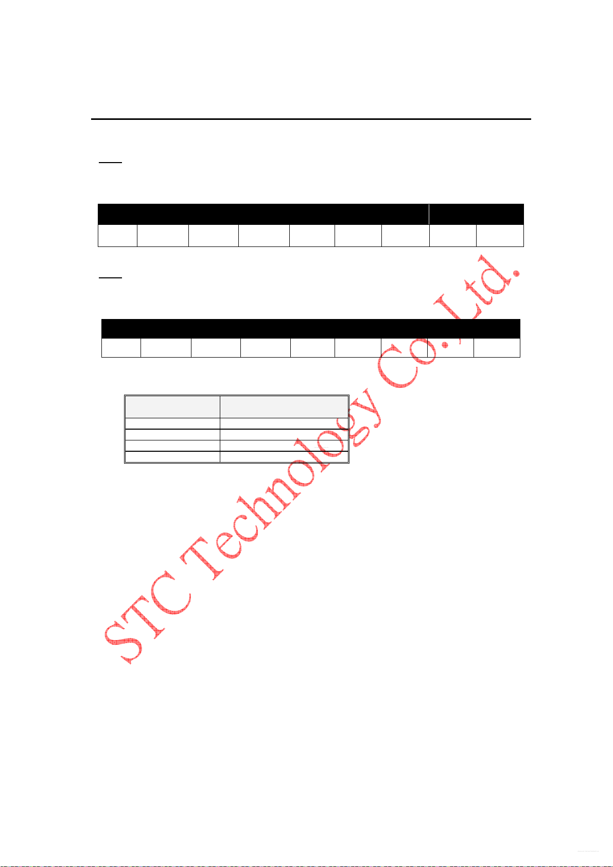
Order Information:
Part Number Temperature
12x5Aaa-bbb-cc-d-eee-ff
12x5Aaa-bbb-cc-d-eee-ff
Range
-40℃~+85℃
-40℃~+85℃
Package Packing Operation
Voltage
PDIP-40 Tray LE3.3V/ C:5V
PLCC-44 Tray LE3.3V/ C:5V
12x5Aaa-bbb-cc-d-eee-ff
12x5Aaa-bbb-cc-d-eee-ff
-40℃~+85℃
-40℃~+85℃
LQFP-48 Tray LE3.3V/ C:5V
LQFP-44 Tray LE3.3V/ C:5V
.x: voltage aa: rom size bbb:ADC,PWM .or. none cc:active frequency
.d: temperature “I” for industrial eeee: package type ff: pin count
4 STC12C5Axx Technical Summary
Page 5

Pin Description
http://www.DataSheet4U.net/
datasheet pdf - http://www.DataSheet4U.net/
Pin Definition
MNEMONIC
Package T ype
PDIP40 PLCC44 PQFP44 LQFP48
P0.0 ~ P0.7 32-39 43-34 37-30 40-33
P1.0 /ADC0/
CLKOUT2
P1.1/ADC1
P1.2/ADC2/ECI/
RXD2
P1.3/ADC3/CCPO/
TXD2
P1.4/ADC4/CCP1/SS
1
2
3
4
5
2
3
4
5
6
40
41
42
43
44
43
44
45
46
47
DESCRIPTION
Port0: Port0 is an open-drain,
bi-directional IO port. When 1s are
written to Port0, they become
high-impedance inputs. Port0 is also
the multiplexed low-order address
and data bus during accesses to
external program and data memory.
Port1: General-purposed I/O with
weak pull-up resistance inside. When
1s are written into Port1, the strong
output driving PMOS only turn-on two
period and then the weak pull-up
resistance keep the port high.
ADCn: Analog to Digital Converter
Input.
P1.5/ADC5/MOSI
P1.6/ADC6/MISO
P1.7/ADC7/SCLK
6
7
8
7
8
9
1
2
3
2
3
4
P2.0 ~ P2.7 21-28 24-31 18-25 19-23
26-28
P3.0/RXD
P3.1/TXD
P3.2/INT0
P3.3/INT1
P3.4/T0/CLKOUT0
P3.5/T1/CLKOUT1
P3.6/WR
P3.7/RD
10-17 11
13
14
15
16
17
18
19
5
7
8
9
10
11
12
13
6
8
9
10
11
12
13
14
Port2: Port2 is an 8-bit bi-directional
I/O port with pull-up resistance.
Except being as GPIO, Port2 emits
the high-order address byte during
accessing to external program and
data memory.
Port3: General-purposed I/O with
weak pull-up resistance inside. When
1s are written into Port1, the strong
output driving PMOS only turn-on two
period and then the weak pull-up
resistance keep the port high. Port3
also serves the special function of
STC12C5Axx.
STC12C5Axx Technical Summary 5
Page 6

http://www.DataSheet4U.net/
datasheet pdf - http://www.DataSheet4U.net/
P4.0/SS
P4.1/ECI/MOSI
P4.2/CCP0/MISO
P4.3/CCP1/SCLK
P4.4/NA
P4.5/ALE
P4.6/EX_LVD/RST2
P4.7/RST
29
30
31
9
23
34
1
12
32
33
35
10
17
28
39
6
26
27
29
4
RESET 9 10 4 5
18
31
42
7
29
30
32
5
Port4: Port4 are extended I/O ports
such like Port1. It can be available
only on 44L-PLCC, 44L-PQFP and
48L-LQFP.
ALE: Address Latch
EX_LVD: External Low Voltage Reset
Detector.
RESET: A high on this pin for at least
two machine cycles will reset the
device.
P5.0
P5.1
P5.2
P5.3
XTAL1 19 21 15 16
24
25
48
1
Port5: Port4 are extended I/O ports
such like Port1. It can be available
only on 48L-LQFP.
Crystal1: Input to the inverting
oscillator amplifier.
XTAL2 18 20 14 15
Crystal2: Output from the inverting
amplifier.
VDD 40 44 38 41
VSS 20 22 16 17
Power
Ground
6 STC12C5Axx Technical Summary
Page 7

Pin Configuration
http://www.DataSheet4U.net/
datasheet pdf - http://www.DataSheet4U.net/
CLKOUT2/P1. 0
P1.1
ECI/P1.2
CCP0/P1.3
SS/CCP1/P1.4
MOSI/P1.5
MISO/P1.6
SCLK/P1.7
RST/P4.7
RXD/P3.0
TXD/P3.1
INT0/P3.2
INT1/P3.3
CLKOUT0/T0/P3.4
CLKOUT1/T1/P3.5
WR/P3. 6
RD/P3.7
XTAL2
XTAL1
GND
1
40
STC12C5Axx
PDIP-40
20 21
VDD
P0.0/AD0
P0.1/AD1
P0.2/AD2
P0.3/AD3
P0.4/AD4
P0.5/AD5
P0.6/AD6
P0.7/AD7
EX_LVD/P4.6/RST2
ALE/P4.5
NA/P4.4
P2.7/A15
P2.6/A14
P2.5/A13
P2.4/A12
P2.3/A11
P2.2/A10
P2.1/A9
P2.0/A8
MISO/CCP0/P4.2
CLKOUT2/P1.0
ECI/P1.2
P1.1
VDD
STC12C5Axx
LQFP-48
XTAL1
GND
P4.0/SS
P2.0/A8
P2.1/A9
AD0/P0.0
AD1/P0.1
AD2/P0.2
AD3/P0.3
P0.4/AD4
P0.5/AD5
P0.6/AD6
P0.7/AD7
P4.6/E_LVD/RST2
P4.1/ECI/MOSI
P4.5/ALE
NA/P4.4
P2.7/A15
P2.6/A14
P2.5/A13
P5.1
P2.2/A10
P2.3/A11
P2.4/A12
P5.0
P5.3
MOSI/P1.5
MISO/P1.6
SCLK/P1.7
RST/P4.7
RXD/P3.0
SCLK/CCP1/P4.3
TXD/P3.1
INT0/P 3.2
INT1/P 3.3
CLKOUT0/T0/P3.4
CLKOUT1/T1/P3.5
SS/CCP1/P1.4
CCP0/P1.3
P5.2
1
P3.6/WR
P3.7/RD
XTAL2
STC12C5Axx Technical Summary 7
Page 8

STC TECHNOLOGY Co.,Ltd.
http://www.DataSheet4U.net/
datasheet pdf - http://www.DataSheet4U.net/
STC12C5A08/16/32/60
8-bit micro-controller
MISO/CCP0/P4.2
SS/CCP1/P1.4
CCP0/P1.3
CLKOUT2/P1.0
AD0/P0.0
AD1/P0.1
AD2/P0.2
ECI/P1.2
P1.1
VDD
AD3/P0.3
MOSI/P1.5
MISO/P1.6
SCLK/P1.7
RST/P4.7
RXD/P3.0
SCLK/CCP1/P4.3
TXD/P3.1
INT0/P3.2
INT1/P3.3
CLKOUT0/T0/P3.4
CLKOUT1/T1/P3.5
MOS I.P1.5
MISO/P1.6
SCLK/P1.7
RST/P4.7
RXD/P3.0
SCLK/CCP1/P4.3
TXD/P3.1
INT0/P 3.2
INT1/P 3.3
CLKOUT0/T0/P3.4
CLKOUT1/T1/P3.5
P2.4/A12
AD3/P0.3
40
29
P2.4/A12
P0.4/AD4
P0.5/AD5
P0.6/AD6
P0.7/AD7
P4.6/EX_LVD/RST2
P4.1/ECI/M OSI
P4.5/ALE
P4.4/NA
P2.7/A15
P2.6/A14
P2.5/A13
P0.4/AD4
P0.5/AD5
P0.6/AD6
P0.7/AD7
EX_LVD/P4.6/RST2
P4.1/ECI/MO SI
P4.5/ALE
NA/P4.4
P2.7/A15
P2.6/A14
P2.5/A13
1
STC12C5Axx
PQFP/LQFP-44
P3.6/WR
P3.7/RD
XTAL2
XTAL1
GND
P4.0/SS
P.0/A8
P2.1/A9
P2.2/A10
P2.3/A11
MISO/CCP0/P4.2
ECI/P1.2
CLKOUT2/P1.0
AD0/P0.0
AD1/P0.1
AD2/P0.2
P1.1
VDD
1
SS/CCP1/P1.4
CCP0/P1.3
7
STC12C5Axx
PLCC-44
18
P3.6/WR
P3.7/RD
XTAL2
XTAL1
GND
P4.0/SS
P2.0/A8
P2.1/A9
P2.2/A10
P2.3/A11
This document contains information on a new product under development by STC.STC reserves the right to change or discontinue this
product without notice. 2007/12 version A1
Page 9

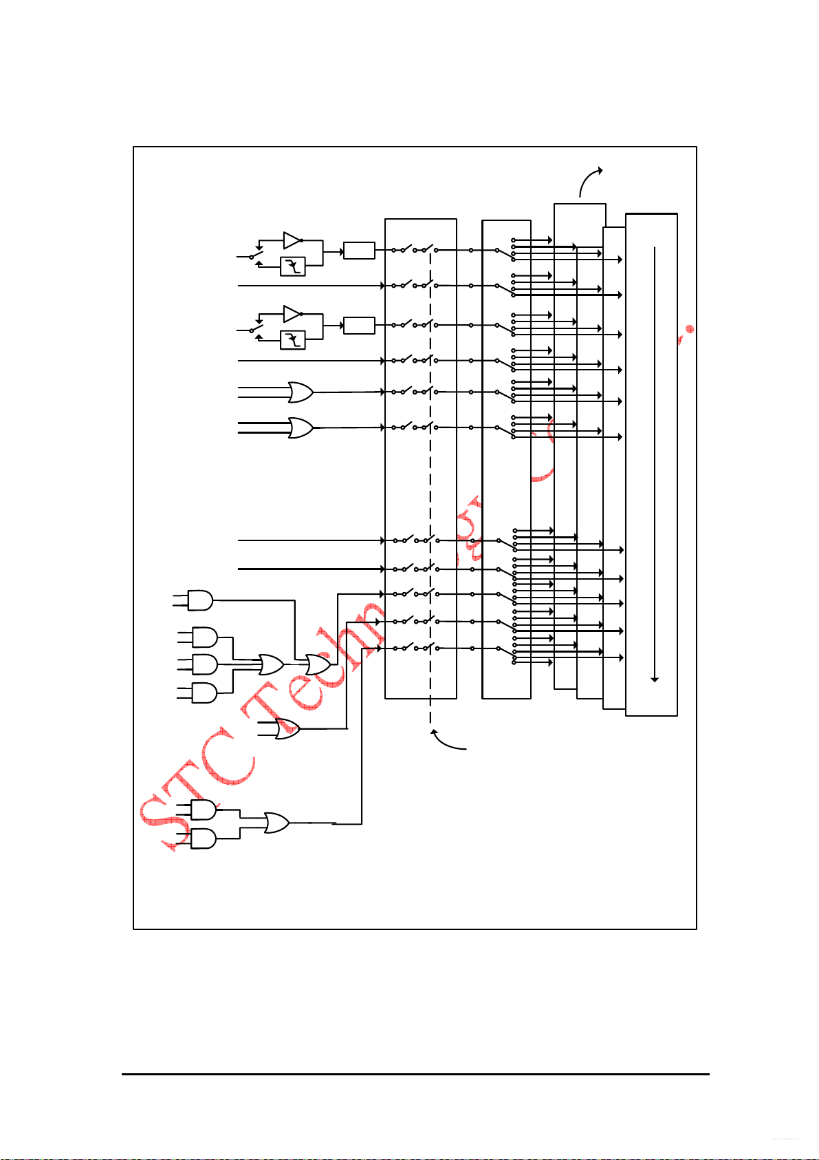
Block Diagram
http://www.DataSheet4U.net/
datasheet pdf - http://www.DataSheet4U.net/
ALU
STC12C5Axx Technical Summary 9
Page 10

http://www.DataSheet4U.net/
datasheet pdf - http://www.DataSheet4U.net/
Special Function Register
Address Map
9 A B C D E F
F8
F0
E8
E0
D8
D0
C8
C0
B8
B0
A8
A0
98
90
88
80
CH CCAP0H CCAP1H
B PCAPWM0*PCAPWM1
*
CL CCAP0L CCAP1L
ACC
CCON CMOD CCAPM0 CCAPM1
PSW
P5 P5M1 P5M0 SPSTAT SPCTL SPDAT
P4 WDT_CONTR IAP_DATA IAP_ADDRH IAP_ADDRL IAP_CMD IAP_TRIG IAP_CONTR
IP SADEN P4SW ADC_CONTR ADC_RES ADC_RESL
P3 P3M1 P3M0 P4M1 P4M0 IP2 IP2H IPHIPH
IE SADDR
P2 BUS_SPEED AUXR1 TEST_WDT
SCON SBUF S2CON S2SBUF BRT P1ASF
P1 P1M1 P1M0 P0M1 P0M0 P2M1 P2M0 CLK_DIV
TCON TMOD TL0 TL1 TH0 TH1 AUXR WAKE_CLK0
P0 SP DPL DPH PCON
* Write Only
10 STC12C5Axx Technical Summary
Page 11

Bits Description
http://www.DataSheet4U.net/
datasheet pdf - http://www.DataSheet4U.net/
SYMBOL ADDRESS
MAP
P0 80H xxxx1111B
SP 81H 00000111B
DPL 82H 00000000B
DPH 83H 00000000B
PCON 87H -- -- -- -- -- -- PD IDL xxxxxx00B
TCON 88H TF1 TR1 TF0 TR0 IE1 IT1 IE0 IT0 00000000B
TMOD 89H GATE C/T M1 M0 GATE C/T M1 M0 00000000B
TL0 8AH 00000000B
TL1 8BH 00000000B
TH0 8CH 00000000B
TH1 8DH 00000000B
AUXR 8EH T0X12 T1X12 UART_ BRTR S2SMOD BRTX12 EXTRAM S1BRS 00xxxxxxB
WAKE_CLKO 8FH PCA RXD_PIN_ T1_PIN_ T0_PIN_ LVD_WA BRTCLK T1CLKO T0CLKO 00000x00B
P1 90H P1.7 P1.6 P1.5 P1.4 P1.3 P1.2 P1.1 P1.0 11111111B
P1M1 91H P1.7M1 P1.6M1 P1.5M1 P1.4M1 P1.3M1 P1.2M1 P1.1M1 P1.0M1 00000000B
P1M0 92H P1.7M0 P1.6M0 P1.5M0 P1.4M0 P1.3M0 P1.2M0 P1.1M0 P1.0M0 00000000B
P0M1 93H P0.7M1 P0.6M1 P0.5M1 P0.4M1 P0.3M1 P0.2M1 P0.1M1 P0.0M1 00000000B
P0M0 94H P0.7M0 P0.6M0 P0.5M0 P0.4M0 P0.3M0 P0.2M0 P0.1M0 P0.0M0 00000000B
P2M1 95H P2.7M1 P2.6M1 P2.5M1 P2.4M1 P2.3M1 P2.2M1 P2.1M1 P2.0M1 00000000B
P2M0 96H P2.7M0 P2.6M0 P2.5M0 P2.4M0 P2.3M0 P2.2M0 P2.1M0 P2.0M0 00000000B
CLK_DIV 97H CLKS2 CLKS1 CLKS0 xxxxx000B
SCON 98H SM0 SM1 SM2 REN TXSTS TISEL TI RI 00000000B
SBUF 99H SD7 SD6 SD5 SD4 SD3 SD2 SD1 SD0 xxxxxxxxB
S2CON 9AH S2SM0 S2SM1 S2SM2 S2REN S2TB8 S2RB8 S2TI S2RI 00000000B
S2SBUF 9BH S2D7 S2D6 S2D5 S2D4 S2D3 S2D2 S2D1 S2D0 xxxxxxxxB
BRT 9CH 00000000B
P1SF 9DH P1.7ASF P1.6ASF P1.5ASF P1.4ASF P1.3ASF P1.2ASF P1.1ASF P1.0ASF 00000000B
P2 A0H P2.7 P2.6 P2.5 P2.4 P2.3 P2.2 P2.1 P2.0 11111111B
BUS_SPEED A1H ALES1 ALES0 RWS2 RWS1 RWS0 xx100x11B
AUXR1 A2H PCA_P4 SPI_P4 S2_P4 GF2 ADRJ DPS 00000000B
TEST_WDT A7H 0xx00000B
IE A8H EA -- ESPI ES ET1 EX1 ET0 EX0 0x000000B
SADDR A9H -- -- -- -- -- 00000000B
IE2 AFH ESPI ES2 xxxxxx00B
P3 B0H P3.7 P3.6 P3.5 P3.4 P3.3 P3.2 P3.1 P3.0 11111111B
P3M1 B1H P3.7M1 P3.6M1 P3.5M1 P3.4M1 P3.3M1 P3.2M1 P3.1M1 P3.0M1 00000000B
P3M0 B2H P3.7M0 P3.6M0 P3.5M0 P3.4M0 P3.3M0 P3.2M0 P3.1M0 P3.0M0 00000000B
P4M1 B3H P4.7M1 P4.6M1 P4.5M1 P4.4M1 P4.3M1 P4.2M1 P4.1M1 P4.0M1 00000000B
P4M0 B4H P4.7M0 P4.6M0 P4.5M0 P4.4M0 P4.3M0 P4.2M0 P4.1M0 P4.0M0 00000000B
IP2 B5H PSP1 PS2 xxxxxx00B
IP2H B6H PSP1H PS2H xxxxxx00B
IPH B7H PPCAH PLVDH PADCH PSH PT1H PX1H PT0H PX0H 00000000B
IP B8H PPCA PLVD PADC PS PT1 PX1 PT0 PX0 00000000B
MSB LSB
BIT ADDRESS AND SYMBOL
INITIAL
VALUE
STC12C5Axx Technical Summary 11
Page 12

http://www.DataSheet4U.net/
datasheet pdf - http://www.DataSheet4U.net/
SADEN B9H 00000000B
P4SW BBH LVD_P4.6 ALE_P4.5 NA/P4.4 x000xxxxB
ADC_CONTR BCH ADC SPEED1 SPEED0 ADC_ ADC_ CHS2 CHS1 CHS0 00000000B
ADC_RES BDH 00000000B
ADC_RESL BEH 00000000B
P4 C0H 11111111B
WDT_CONTR C1H WDT_ -- EN_WDT CLR_ IDL_ PS2 PS1 PS0 xx000000B
IAP_DATA C2H 11111111B
IAP_ADDRESS C3H 00000000B
IAP ADDRESS C4H 00000000B
IAP CMD C5H MS1 MS0 xxxxxx00B
IAP_TRIG C6H xxxxxxxxB
IAP_CONTR C7H IAPEN SWBS SWRST CMD_Fail WT2 WT1 WT0 00001000B
P5 C8H
P5M1 C9H P5.7M1 P5.6M1 P5.5M1 P5.4M1 P5.3M1 P5.2M1 P5.1M1 P5.0M1 xxxx0000B
P5M0 CAH P5.7M0 P5.6M0 P5.5M0 P5.4M0 P5.3M0 P5.2M0 P5.1M0 P5.0M0 xxxx0000B
SPSTAT CDH SPIF WCOL 00xxxxxxB
SPCTL CEH SSIG SPEN DORD MSTR CPOL CPHA SPR1 SPR0 00000100B
SPDAT CFH 0000000B
PSW D0H CY AC F0 RS1 RS0 OV -- P 00000000B
CCON D8H CF CR CCF1 CCF0 00xxxx00B
CMOD D9H CIDL CPS2 CPS1 CPS0 ECF 0xxx0000B
CCAPM0 DAH ECOMO CAPP0 CAPN0 MAT0 TOG0 PWM0 ECCF0 x0000000B
CCAPM1 DBH ECOM1 CAPP1 CAPN1 MAT1 TOG1 PWM1 ECCF1 x0000000B
ACC E0H 00000000B
CL E9H WRF -- ENW CLW WIDL PS2 PS1 PS0 0x000000B
CCAP0L EAH 11111111B
CCAP1L EBH 00000000B
B F0H 00000000B
PCA_PWM0 F2H -- -- -- -- -- -- EPC0H EPC0L xxxxxx00B
PCA_PWM1 F3H EPC1H EPC1L xxxxxx00B
CH F9H 00000000B
CCAP0H FAH 00000000B
CCAP1H FBH 00000000B
12 STC12C5Axx Technical Summary
Page 13

http://www.DataSheet4U.net/
datasheet pdf - http://www.DataSheet4U.net/
Memory
Organization
STC TECHNOLOGY Co.,Ltd.
STC12C5A08/16/32/60
8-bit micro-controller
00
7F
80
FF
Address Space for STC12C5Axx RAM
RAM
There are 1280 bytes RAM built in STC12C5Axx.
00-7F RAM, Access it via direct addressing
80-FF SFR, Access it via direct addressing
80-FF indirect on-chip RAM,
Access it via indirect addressing
0000-03FF On-Chip External auxiliary RAM.
The user can visit the leading 128-byte RAM via direct addressing instructions, we name those RAM as
direct RAM that occupies address space 00h to 7Fh.
Followed 128-byte RAM can be visited via indirect addressing instructions, we name those RAM as
indirect RAM that occupied address space 80h to FFh.
There are extra 1024 bytes RAM can be visited via MOVX @Ri or @DPTR instructions which are
named external or auxiliary RAM. None of P0 status and P2 status will be affected during MOVX
instruction.
A control bit EXTRAM located in SFR AUXR.1 register is to control access of auxiliary RAM. When set,
disable the access of auxiliary RAM. When clear (EXTRAM=0), this auxiliary RAM is the default target
for the address range from 0x0000 to 0x03FF. If EXTRAM=0 and the target address is over 0x03FF,
STC12C5Axx switches to access external RAM automatically. When EXTRAM=0, the content in DPH is
ignored when the instruction MOVX @Ri is executed.
This document contains information on a new product under development by STC.STC reserves the right to change or discontinue this
product without notice. 2007/12 version A1
Page 14

http://www.DataSheet4U.net/
datasheet pdf - http://www.DataSheet4U.net/
Embedded Flash
There is totally 64K byte flash embedded in the STC12C5Axx.
The user can configure the whole flash to store his application program, or he can configure
the flash for both storage of application (AP) program and In-System-Program (ISP) code,
even he can configure the flash for storage of AP, ISP, and In-Application-Program (IAP)
memory.
If there is requirement from the user’s application program to store nonvolatile parameters,
the user can allocate part of the embedded flash as IAP memory by Part No..
14 STC12C5Axx Technical Summary
Page 15

STC TECHNOLOGY Co.,Ltd.
http://www.DataSheet4U.net/
datasheet pdf - http://www.DataSheet4U.net/
STC12C5A08/16/32/60
8-bit micro-controller
ALE OUTPUT
As we have known, an 8051 MCU always outputs ALE the signal. However, the device doesn’t
output the ALE signal except when accessing the external data memory.
Access Timing Stretching for Low-speed Memory
To access the low-speed external data memory, the timing-stretch mechanism is designed to
control the access timing of the “MOVX” instructions. The bits ALES1 and ALES0, in
BUS_SPEED register, control the stretching of the setup time and hold time with respect to ALE
negative edge. And, the bits RWS2, RWS1 and RWS0 control the stretching of the read/write
pulse width. Users should configure STRETCH register properly to conform to the read/write
requirements of the external data memory being used.
BUS_SPEED (Address=A1H, External Access Stretch Register)
BUS_SPEED register
Read/Write Address: 0XA1H
Default: XX10-X011
Bit 7 6 5 4 3 2 1 0
Name
Note:The reset value for BUS_SPEED is 00100011b (0x23). That is, {ALES1,ALES0}={1,0} and
ALES1 ALES0
RWS2
RWS1 RWS0
{RWS2,RWS1,RWS0}={0,1,1}.
{ALES1, ALES0}:
00: No stretch, the P0’s address setup/hold time to the following ALE falling edge is 1 clock cycle.
01: 1 clock stretched, the P0’s address setup/hold time to the following ALE falling edge is 2 clock cycles.
10: 2 clocks stretched, the P0’s address setup/hold time to the following ALE falling edge is 3 clock
cycles.
11: 3 clocks stretched, the P0’s address setup/hold time to the following ALE falling edge is 4 clock
cycles.
{RWS2, RWS1, RWS0}:
000: No stretch, the MOVX read/write pulse is 1 clock cycle.
001: 1 clock stretched, the MOVX read/write pulse is 2 clock cycles.
010: 2 clocks stretched, the MOVX read/write pulse is 3 clock cycles.
This document contains information on a new product under development by STC.STC reserves the right to change or discontinue this
product without notice. 2007/12 version A1
Page 16

http://www.DataSheet4U.net/
datasheet pdf - http://www.DataSheet4U.net/
011: 3 clocks stretched, the MOVX read/write pulse is 4 clock cycles.
100: 4 clocks stretched, the MOVX read/write pulse is 5 clock cycles.
101: 5 clocks stretched, the MOVX read/write pulse is 6 clock cycles.
110: 6 clocks stretched, the MOVX read/write pulse is 7 clock cycles.
111: 7 clocks stretched, the MOVX read/write pulse is 8 clock cycles.
16 STC12C5Axx Technical Summary
Page 17

Functional Description
http://www.DataSheet4U.net/
datasheet pdf - http://www.DataSheet4U.net/
I/O Port Configuration
There are 44(max) port pins on STC12C5Axx may be independently configured to one of four
modes: quasi-bidirectional(standard 8051 port output), push-pull output, open-drain output or
input-only. All port pins default to quasi-bidirectional after reset. Each port pin has a
Schmitt-triggered input for improved input noise rejection. During power-down, all the
schmitt-triggered inputs are disabled with the exception o
RXD_PIN to drive this device escape power-down mode. Therefore such kind of pins should not be left
floating during power-down.
f P3.2 (INT0) and P3.3 (INT1) or
There are several special function registers designed to configure those I/O ports.
P0M0(P0 Configuration 0)
SFR:
Read/Write Address: 0X94H
Default: 0000-0000
Bit 7 6 5 4 3 2 1 0
Name
P0M0.7 P0M0,6 P0M0.5 P0M0.4 P0M0.3 P0M0.2 P0M0.1 P0M0.0
SFR: P0M1(P0 Configuration 1)
Read/Write Address: 0X93H
Default: 0000-0000
Bit 7 6 5 4 3 2 1 0
Name
P0M1.7 P0M1,6 P0M1.5 P0M1.4 P0M1.3 P0M1.2 P0M1.1 P0M1.0
SFR: P1M0(P1 Configuration 0)
Read/Write Address: 0X92H
Default: 0000-0000
Bit 7 6 5 4 3 2 1 0
Name
P1M0.7 P1M0,6 P1M0.5 P1M0.4 P1M0.3 P1M0.2 P1M0.1 P1M0.0
SFR: P1M1(P1 Configuration 1)
Read/Write Address: 0X91H
Default: 0000-0000
Bit 7 6 5 4 3 2 1 0
Name
P1M1.7 P1M1,6 P1M1.5 P1M1.4 P1M1.3 P1M1.2 P1M1.1 P1M1.0
SFR: P3M0(P3 Configuration 0)
Read/Write Address: 0XB2H
Default: 0000-0000
Bit 7 6 5 4 3 2 1 0
Name
P3M0.7 P3M0,6 P3M0.5 P3M0.4 P3M0.3 P3M0.2 P3M0.1 P3M0.0
STC12C5Axx Technical Summary 17
Page 18

http://www.DataSheet4U.net/
datasheet pdf - http://www.DataSheet4U.net/
SFR:
P3M1(P3 Configuration 1)
Read/Write Address: 0XB1H
Default: 0000-0000
Bit 7 6 5 4 3 2 1 0
Name
P3M1.7 P3M1,6 P3M1.5 P3M1.4 P3M1.3 P3M1.2 P3M1.1 P3M1.0
SFR: P4M0(P4 Configuration 0)
Read/Write Address: 0XB4H
Default: 0000-0000
Bit 7 6 5 4 3 2 1 0
Name
P4M0.7 P4M0,6 P4M0.5 P4M0.4 P4M0.3 P4M0.2 P4M0.1 P4M0.0
SFR: P4M1(P4 Configuration 1)
Read/Write Address: 0XB3H
Default: 0000-0000
Bit 7 6 5 4 3 2 1 0
Name
P4M1.7 P4M1,6 P4M1.5 P4M1.4 P4M1.3 P4M1.2 P4M1.1 P4M1.0
SFR: P5M0(P5 Configuration 0)
Read/Write Address: 0XCAH
Default: 0000-0000
Bit 7 6 5 4 3 2 1 0
Name
P5M0.7 P5M0,6 P5M0.5 P5M0.4 P5M0.3 P5M0.2 P5M0.1 P5M0.0
SFR: P5M1(P5 Configuration 1)
Read/Write Address: 0XC9H
Default: 0000-0000
Bit 7 6 5 4 3 2 1 0
Name
P5M1.7 P5M1,6 P5M1.5 P5M1.4 P5M1.3 P5M1.2 P5M1.1 P5M1.0
Configuration of I/O port
PxM0n PxM1n Port Mode
0 0
0 1
1 0
1 1
( x = 1 or 3 n = 7, 6, 5, 4, 3, 2, 1 or 0)
Quasi-bidirectional(default)
Push-Pull output
Input Only (High-impedance)
Open-Drain Output
18 STC12C5Axx Technical Summary
Page 19

Quasi-bidirectional Mode
http://www.DataSheet4U.net/
datasheet pdf - http://www.DataSheet4U.net/
Port pins in quasi-bidirectional output mode function similar to the standard 8051 port pins. A
quasi-bidirectional port can be used as an input and output without the need to reconfigure the
port. This is possible because when the port outputs logic high, it is weakly driven, allowing an
external device to pull the pin low. When the pin outputs low, it is driven strongly and able to
sink a large current. There are three pull-up transistors in the quasi-bidirectional output that
serve different purposes.
One of these pull-ups, called the “very weak” pull-up, is turned on whenever the port register
for the pin contains a logic “1”. This very weak pull-up sources a very small current that will
pull the pin high if it is left floating.
A second pull-up, called the “weak” pull-up, is turned on when the port register for the pin
contains a logic “1” and the pin itself is also at a logic “1” level. This pull-up provides the
primary source current for a quasi-bidirectional pin that is outputting a ‘1’. If this pin is pulled
low by the external device, this weak pull-up turns off, and only the very weak pull-up remains
on. In order to pull the pin low under these conditions, the external device has to sink enough
current to over-power the weak pull-up and pull the port pin below its input threshold voltage.
The third pull-up is referred to as the “strong” pull-up. This pull-up is used to speed up
low-to-high transitions on a quasi-bidirectional port pin when the port register changes from a
logic “0” to a logic “1”. When this occurs, the strong pull-up turns on for two CPU clocks,
quickly pulling the port pin high.
VDDVDD VDD
2 clocks
delay
Strong Very weak
Port latch data
Weak
Port pin
Input data
STC12C5Axx Technical Summary 19
Page 20

http://www.DataSheet4U.net/
datasheet pdf - http://www.DataSheet4U.net/
Open-drain Output
The open-drain output configuration turns off all pull-ups and only drives the pull-down
transistor of the port pin when the port register contains logic “0”. To use this configuration in
application, a port pin must have an external pull-up, typically tied to VDD. The input path of
the port pin in this configuration is the same as quasi-bidirection mode.
Port pin
Port latch data
Input data
Input-only Mode
The input-only configuration is a Schmitt-triggered input without any pull-up resistors on the
pin.
Input data
Port pin
Push-pull Output
The push-pull output configuration has the same pull-down structure as both the open-drain
and the quasi-bidirectional output modes, but provides a continuous strong pull-up when the
port register contains a logic “1”. The push-pull mode may be used when more source current
is needed from a port output.
VDD
Port latch data
Port pin
Input data
20 STC12C5Axx Technical Summary
Page 21

Timer/Counter
http://www.DataSheet4U.net/
datasheet pdf - http://www.DataSheet4U.net/
STC12C5Axx has two 16-bit timers, and they are named T0 and T1. Each of them can also
be used as a general event counter, which counts the transition from 1 to 0.
Since the STC12C5Axx is a RISC-like MCU which execute faster than traditional 80C51 MCU
from other providers. Based on consideration of compatibility with traditional 80C51 MCUs,
the frequency of the clock source for T0 and T1 is designed to be selectable between
oscillator frequency divided-by-12 (default) or oscillator frequency.
The user can configure T0/T1 to work under mode-0, mode-1, mode-2 and mode-3. It is fully
the same to a traditional 80C51 MCU.
There are two SFR designed to configure timers T0 and T1. They are TMOD, TCON.
The user also should take a glace of SFR AUXR which decide the frequency of the clock
source driving the T0 and T1.
SFR:
TMOD(Timer Mode Control Register)
Read/Write Address: 0X89H
Default: 0000-0000
Bit 7 6 5 4 3 2 1 0
Name
GATE: = Gating control
C//T: = Timer or Counter function selector. 0: =timer, 1: =counter
{M1, M0}: mode select
GATE
0: = (default)
Timer x is enabled whenever “TRx” control bit is set.
1: =
Timer/Counter x is enabled only while “/INTx” pin is high and “TRx” control bit is set.
0: = (default)
Configure Tx as Timer use
1: =
Configure Tx as Counter use
{0, 0}: =
Configure Tx as 13-bit timer/counter
{0, 1}: =
Configure Tx as 16-bit timer/counter
{1, 0}: =
Configure Tx as 8-bit timer/counter with automatic reload capability
{1, 1}: =
for T0, set TL0 as 8-bit timer/counter, TH0 is locked into 8-bit timer
for T1, set Timer/Counter1 Stopped
For Timer-1 Only For Timer-0 Only
C//T
M1 M0 GATE
C//T
M1 M0
STC12C5Axx Technical Summary 21
Page 22

http://www.DataSheet4U.net/
datasheet pdf - http://www.DataSheet4U.net/
SFR:
TCON
Read/Write Address: 0X88H
Default: 0000-0000
Bit 7 6 5 4 3 2 1 0
Name
TF1 TR1 TF0 TR0 IE1 IT1 IE01 IT0
TF1: = Timer1 overflow flag.
This bit is automatically set by hardware on T1 overflow, and will be automatically cleared by
hardware when the processor vectors to the interrupt routine.
TR1: = Timer1 run control bit.
0: = (default)
Stop T1 counting
1: =
Start T1 counting
TF0: = Timer0 overflow flag.
This bit is automatically set by hardware on T0 overflow, and will be automatically cleared by
hardware when the processor vectors to the interrupt routine.
TR0: = Timer0 run control bit.
0: = (default)
Stop T0 counting
1: =
Start T0 counting
IE1: = External Interrupt-1 flag.
This bit is automatically set by hardware on interrupt from the external interrupt-1, and will be
automatically cleared by hardware when the processor vectors to the interrupt routine.
IT1: = Interrupt-1 type control bit.
0: = (default)
Set the interrupt-1 triggered by low duty from pin EX1
1: =
Set the interrupt-1 triggered by negative falling edge from pin EX1
IE0: = External Interrupt-0 flag.
This bit is automatically set by hardware on interrupt from the external interrupt-0, and will be
automatically cleared by hardware when the processor vectors to the interrupt routine.
IT0: = Interrupt-0 type control bit.
0: = (default)
Set the interrupt-0 triggered by low duty from pin EX1
1: =
Set the interrupt-0 triggered by negative falling edge from pin EX1
22 STC12C5Axx Technical Summary
Page 23

SFR:
http://www.DataSheet4U.net/
datasheet pdf - http://www.DataSheet4U.net/
AUXR (Auxiliary Register)
Read/Write Address: 0x8EH
Default: 00XX-XXXX
Bit 7 6 5 4 3 2 1 0
Name
T0X12 T1X12 UARTM0X6 BRTR S2SMOD BRTRX12 EXTRAM S1BRS
T0X12: = T0 clock source selector
0: = (default)
Set the frequency of the clock source for T0 as the oscillator frequency divided-by-12.
It will compatible to the traditional 80C51 MCU.
1: =
Set the frequency of the clock source for T0 as the oscillator frequency.
It will drive the T0 faster than a traditional 80C51 MCU.
T1X12: = T1 clock source selector
0: = (default)
Set the frequency of the clock source for T1 as the oscillator frequency divided-by-12.
It will compatible to the traditional 80C51 MCU.
1: =
Set the frequency of the clock source for T1 as the oscillator frequency.
It will drive the T1 faster than a traditional 80C51 MCU.
UARTM0X6: = Baud rate selector of UART while it is working under Mode-0
0: = (default)
Set the baud rate of the UART functional block as oscillator frequency divided-by-12.
It will compatible to the traditional 80C51 MCU.
1: =
Set the baud rate of the UART functional block as oscillator frequency divided-by-2.
It will transmit/receive data faster than a traditional 80C51 MCU.
BRTR: = Setting this bit will enable the baud-rate generator of UART2 to run.
S2SMOD: = Setting this bit can double up the baud-rate of UART2.
BRTRX12: = Set this bit to set the clock source for the UART2 is BRT, or clear it to set the clock
source for or the UART2 as BRT/12.
S1BRS: = S1 Baud-Rate clock source selector
0: = (default)
Select timer-1 for baud-rate clock source to S1
1: =
Select BRT for baud-rate clock source to S1
STC12C5Axx Technical Summary 23
Page 24

x
/
/
http://www.DataSheet4U.net/
datasheet pdf - http://www.DataSheet4U.net/
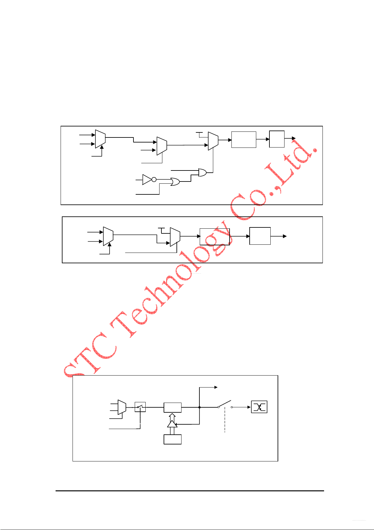
Mode 0
The timer register is configured as a 13-bit register. As the count rolls over from all 1s to all 0s,
it sets the timer interrupt flag TFx. The counted input is enabled to the timer when TRx = 1
and either GATE=0 or INTx = 1. Mode 0 operation is the same for Timer0 and Timer1.
OSC/12
OSC
AUXR.x
0
1
T0 or T1 pin
(sampled)
C
GATE
/INTx
0
1
T
TR
0
1
TLx[4:0] THx[7:0]
TFx
Mode 1
Mode1 is the same as Mode0, except that the timer register is being run with all 16 bits.
OSC/12
OSC
AUXR.x
0
1
T0 or T1 pin
(sampled)
0
1
0
1
TLx[7:0] THx[7:0]
TFx
Interrupt
Interrupt
GATE
/INTx
Mode 2
Mode 2 configures the timer register as an 8-bit counter (TLx) with automatic reload. Overflow
from TLx does not only set TFx, but also reloads TLx with the content of THx, which is
determined by user’s program. The reload leaves THx unchanged. Mode 2 operation is the
same for Timer0 and Timer1.
OSC/12
OSC
AUXR.x
0
1
T0 or T1 pin
(sampled)
GATE
/INTx
0
1
0
1
TLx [7:0]
THx [7:0]
Reload
TFx
Interrupt
24 STC12C5Axx Technical Summary
Page 25
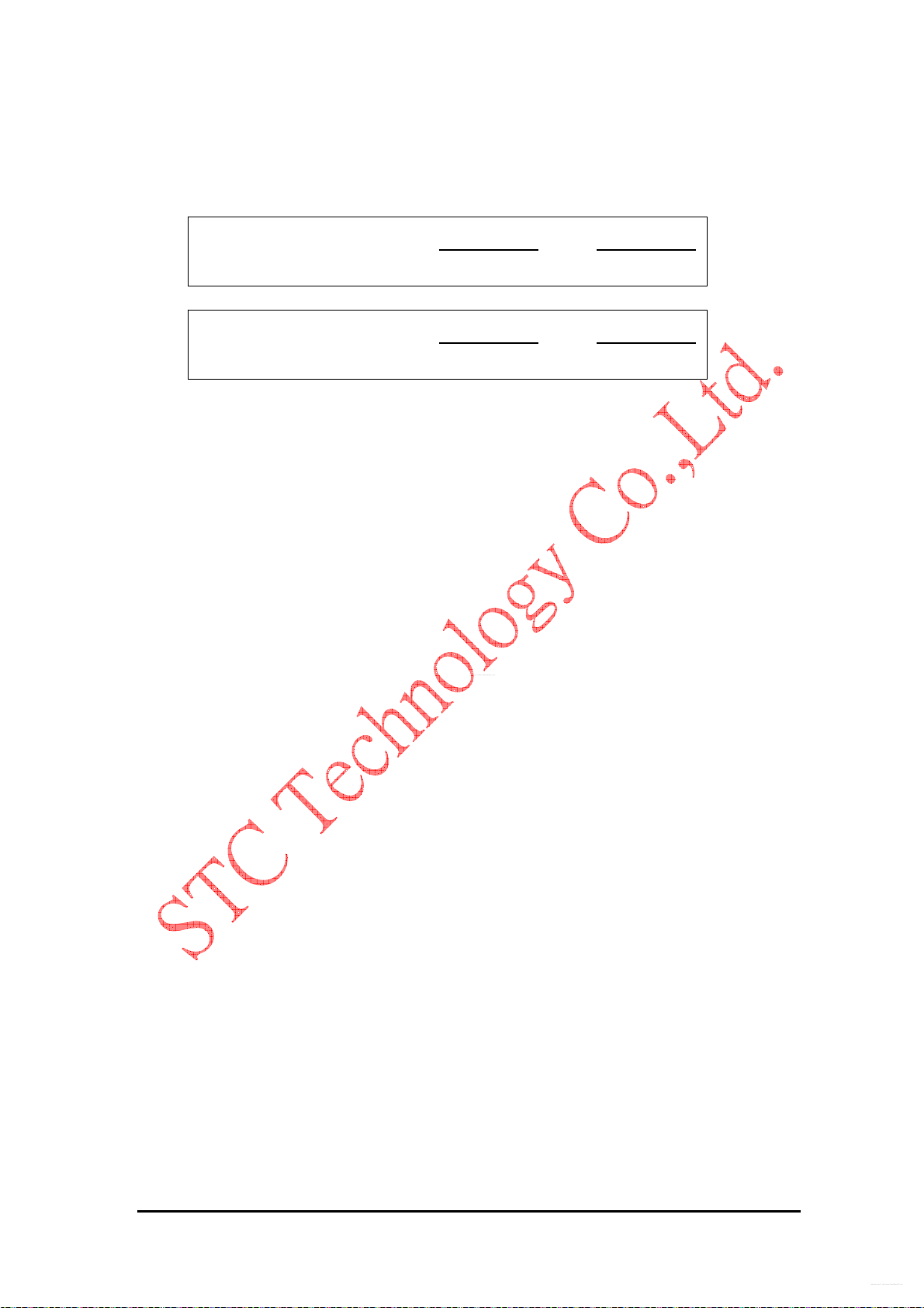
Mode 3
http://www.DataSheet4U.net/
datasheet pdf - http://www.DataSheet4U.net/
Timer1 in Mode3 simply holds its count, the effect is the same as setting TR1 = 1. Timer0 in
Mode 3 enables TL0 and TH0 as two separate 8-bit counters. TL0 uses the Timer0 control bits
such like C/T, GATE, TR0, INT0 and TF0. TH0 is locked into a timer function (can not be
external event counter) and take over the use of TR1, TF1 from Timer1. TH0 now controls the
Timer1 interrupt.
OSC/12
OSC
AUXR.x
0
1
Sampled T0 pin
0
1
0
1
TL0 [7:0]
TF0
Interrupt
GATE
/INT0
OSC/12
OSC
AUXR.x
0
1
TR1
0
1
TH0 [7:0]
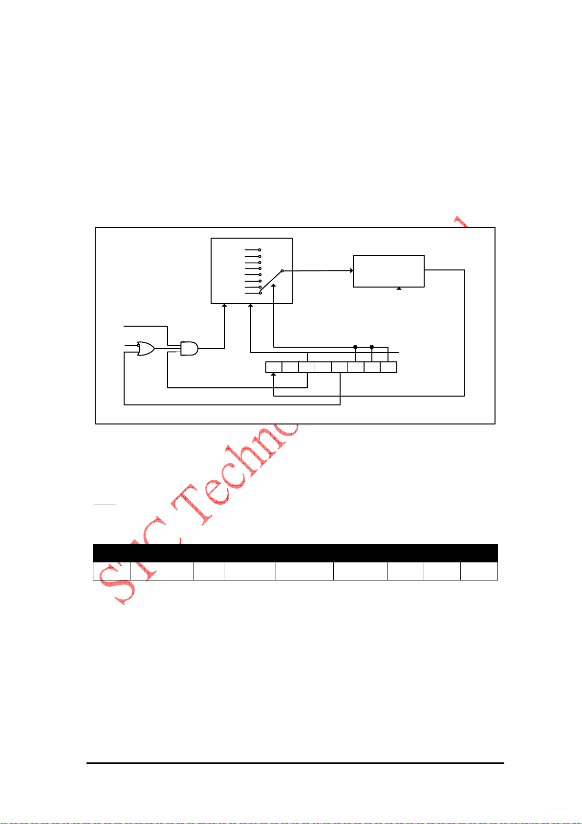
BAUD-RATE GENERATOR(BRT)
BAUD-RATE GENERATOR(BRT)
Baud-Rate Generator and P1.0/P4.1 programmable clock output
TF1
Interrupt
BRTCLKO
To UART
toggle
P1.0 or
P4.1
Fosc/12
Fosc01
S2TX12
BRTR
8-bit timer
BRT
Overflow
Baud-Rate Generator for th e UART
STC12C5Axx Technical Summary 25
Page 26
r
r
http://www.DataSheet4U.net/
datasheet pdf - http://www.DataSheet4U.net/
STC12C5Axx is able to generate a programmable clock output on P1.0 or P4.1. When BRTCLKO bit
in WAKE_CLKO is set, BRT timer overflow pulse will toggle P1.0 or P4.1 latch to generate a 50%
duty clock. The frequency of clock-out is as following :
BRT timer overflow rate =
Fosc
o
256 – BRT
Fosc/12
256 – BRT
P1.0 / P4.1 Clock output frequency =
Fosc /2
256 – BRT
o
Fosc/24
256 – BRT
26 STC12C5Axx Technical Summary
Page 27
Interrupt
http://www.DataSheet4U.net/
datasheet pdf - http://www.DataSheet4U.net/
There are 10 interrupt sources available in STC12C5Axx. Each interrupt source can be individually
enabled or disabled by setting or clearing a bit in the SFR named IE. This register also contains a global
disable bit (EA), which can be cleared to disable all interrupts at once.
Each interrupt source has two corresponding bits to represent its priority. One is located in SFR named
IPH and the other in IP register. Higher-priority interrupt will be not interrupted by lower-priority interrupt
request. If two interrupt requests of different priority levels are received simultaneously, the request of
higher priority is serviced. If interrupt requests of the same priority level are received simultaneously, an
internal polling sequence determine which request is serviced. The following table shows the internal
polling sequence in the same priority level and the interrupt vector address.
Source Vector address Priority within level
/INT0 03H 0 (highest)
Timer 0 0BH 1
/INT1 13H 2
Timer1 1BH 3
UART 23H 4
ADC 2BH 5
LVD 33H 6
PCA 3BH 7
UART2 43H 8
SPI 4BH 9
The external interrupt /INT0, and /INT1 can each be either level-activated or transition-activated,
depending on bits IT0 and IT1 in register TCON. The flags that actually generate these interrupts are bits
IE0 and IE1 in TCON. When an external interrupt is generated, the flag that generated it is cleared by
the hardware when the service routine is vectored to only if the interrupt was transition –activated,
otherwise the external requesting source is what controls the request flag, rather than the on-chip
hardware.
The Timer0 and Timer1 interrupts are generated by TF0 and TF1, which are set by a rollover in their
respective Timer/Counter registers in most cases. When a timer interrupt is generated, the flag that
generated it is cleared by the on-chip hardware when the service routine is vectored to.
The serial port interrupt is generated by the logical “1” of RI and TI. Neither of these flags is cleared by
hardware when the service routine is vectored to. The service routine should poll RI and TI to determine
which one to request service and it will be cleared by software.
The SPI interrupt is generated by the flag SPIF. It can only be cleared by writing a “1” to SPIF bit in
software.
The ADC interrupt is generated by the flag ADC_FLAG. It should be cleared by software.
STC12C5Axx Technical Summary 27
Page 28

http://www.DataSheet4U.net/
datasheet pdf - http://www.DataSheet4U.net/
The PCA interrupt is generated by the logical OR of CF, CCF0 ~ CCF1. The service routine should poll
CF and CCF0 ~ CCF1 to determine which one to request service and it will be cleared by software.
The Low Voltage Detect interrupt is shared by the flag LVDF in PCON.5 register. They should be cleared
by software.
The UART2 interrupt is generated by the logical “1” of S2RI and S2TI. Neither of these flags is cleared
by hardware when the service routine is vectored to. The service routine should poll S2RI and S2TI to
determine which one to request service and it will be cleared by software.
All of the bits that generate interrupts can be set or cleared by software, with the same result as though it
had been set or cleared by hardware. In other words, interrupts can be generated or pending interrupts
can be canceled in software.
How does the STC12C5Axx take the Interrupts
External interrupt pins and other interrupt sources are sampled at rising edge of each clock cycle. The
samples are polled during the next clock cycle. If one of the flags was in a set condition of the first cycle,
the second cycle of polling cycles will find it and the interrupt system will generate an hardware LCALL to
the appropriate service routine as long as it is not blocked by any of the following conditions.
The 2B
interrupt is shared by the logical “1” of ADC interrupt and interrupt. Neither of these flags is
H
cleared by hardware when the service routine is vectored to. The service routine should poll them to
determine which one to request service and it will be cleared by software.
The 4BH interrupt is shared by the logical “1” of SPI interrupt and interrupt. Neither of these flags is
cleared by hardware when the service routine is vectored to. The service routine should poll them to
determine which one to request service and it will be cleared by software.
The 33H interrupt is shared by the logical “1” of LVD interrupt (Low-Voltage Detector) interrupt. Neither of
these flags is cleared by hardware when the service routine is vectored to. The service routine should
poll them to determine which one to request service and it will be cleared by software.
The 3BH interrupt is shared by the logical “1” of PCA interrupt and interrupt. Neither of these flags is
cleared by hardware when the service routine is vectored to. The service routine should poll them to
determine which one to request service and it will be cleared by software.
All of the bits that generate interrupts can be set or cleared by software, with the same result as though it
had been set or cleared by hardware. In other words, interrupts can be generated or pending interrupts
can be canceled in software.
28 STC12C5Axx Technical Summary
Page 29
STC TECHNOLOGY Co.,Ltd.
http://www.DataSheet4U.net/
datasheet pdf - http://www.DataSheet4U.net/
STC12C5A08/16/32/60
8-bit micro-controller
If one of the following conditions happens, a coming interrupt will be blocked.
An interrupt of equal or higher priority level is already in progress.
The current cycle(polling cycle) is not the final cycle in the execution of the instruction in
progress.
The instruction in progress is RETI or any write to SFRs IE, IP, IP2, IPH and IP2H registers.
Condition 2 ensures that the instruction in progress will be completed before vectoring into any service
routine. Condition 3 ensures that if the instruction in progress is RETI or any access to SFRs IE, IP, IP2,
IPH or IP2H, then at least one or more instruction will be executed before any interrupt is vectored to.
The following content describes several SFR related to interrup t mechanism.
SFR: PSW(Program Status Word)
Read/Write Address: 0XD0H
Default: XXXX-XX00
Bit 7 6 5 4 3 2 1 0
Name
CY: = Carry flag.
AC: = Auxilliary Carry Flag.(For BCD operations)
EADC: = Interrupt controller of A/D Converter (ADC).
F0: = Flag 0.(Available to the user for general purposes)
RS1: = Register bank select control bit 1.
RS0: = Register bank select control bit 0.
OV : = Overflow flag.
F1 : = Flag 1. User-defined flag.
P : = Parity flag.
CY AC F0 RS1 RS0 OV F1 P
0: = (default)
Disable
1: =
Enable
This document contains information on a new product under development by STC.STC reserves the right to change or discontinue this
product without notice. 2007/12 version A1
Page 30
http://www.DataSheet4U.net/
datasheet pdf - http://www.DataSheet4U.net/
SFR: IE(Interrupt Enable)
Read/Write Address: 0XA8H
Default: XXXX-XX00
Bit 7 6 5 4 3 2 1 0
Name
EA ELVD EADC ES ET1 EX1 ET0 EX0
EA
: = Global interrupt controller.
0: = (default)
Disable all interrupts
1: =
Release interrupt control to all individual interrupt controllers.
ELVD
: = Interrupt controller of Low-Voltage Detector
0: = (default)
Disable
1: =
Enable
EADC: =
Interrupt controller of A/D Converter (ADC).
0: = (default)
Disable
1: =
Enable
ES: = Interrupt controller of Universal Asynchronous Receiver/Transmitter (UART).
0: = (default)
Disable
1: =
Enable
ET1: = Interrupt controller of Timer-1 interrupt.
0: = (default)
Disable
1: =
Enable
EX1: = Interrupt controller of external interrupt-1.
0: = (default)
Disable
1: =
Enable
ET0: = Interrupt controller of Timer-0 interrupt.
0: = (default)
Disable
1: =
Enable
EX0: = Interrupt controller of external interrupt-0.
0: = (default)
Disable
1: =
30 STC12C5Axx Technical Summary
Page 31
Enable
http://www.DataSheet4U.net/
datasheet pdf - http://www.DataSheet4U.net/
SFR: IP(Interrupt Priority Low)
Read/Write Address: 0xB8H
Default: 0000-0000
Bit 7 6 5 4 3 2 1 0
Name
PPCA PLVDI PADC PS PT1 PX1 PT0 PX0
PPCA: = If set, Set priority for PCA interrupt higher
PLVD: = If set, Set priority for Low Voltage interrupt higher
PADC: = If set, Set priority for ADC interrupt highe
PS: = If set, Set priority for serial port interrupt higher(UART)
PT1: = If set, Set priority for timer1 interrupt higher
PX1: = If set, Set priority for external interrupt 1 higher
PT0: =
If set, Set priority for timer0 interrupt higher
PX0: = If set, Set priority for external interrupt 0 higher
SFR: IPH (Interrupt Priority High)
Read/Write Address: 0XB7H
Default: 0000-0000
Bit 7 6 5 4 3 2 1 0
Name
PPCAH PLVDH PADCH PSH PT1H PX1H PT0H PX0H
PPCAH: = If set, Set priority for PCA interrupt higher
PLVDH: = If set, Set priority for Low Voltage interrupt higher
PADC: = If set, Set priority for ADC interrupt higher
PSH: = If set, Set priority for serial port interrupt higher (UART)
PT1H: = If set, Set priority for timer1 interrupt higher
PX1H: = If set, Set priority for external interrupt 1 higher
PT0H: = If set, Set priority for timer0 interrupt higher
PX0H: = If set, Set priority for external interrupt 0 higher
STC12C5Axx Technical Summary 31
Page 32
STC TECHNOLOGY Co.,Ltd.
http://www.DataSheet4U.net/
datasheet pdf - http://www.DataSheet4U.net/
STC12C5A08/16/32/60
8-bit micro-controller
SFR: IP2 (Interrupt Priority High)
Read/Write Address: 0XB6H
Default: 0000-0000
Bit 7 6 5 4 3 2 1 0
Name
PSPI PS2
SFR: IP2H (Interrupt Priority High)
Read/Write Address: 0XB7H
Default: 0000-0000
Bit 7 6 5 4 3 2 1 0
Name
IP and IPH are combined to form 4-level priority interrupt as the following table.
PSPIH PS2H
{IPH.x, IP.x}
11 1 (highest)
10 2
01 3
00 4
Priority
Level
This document contains information on a new product under development by STC.STC reserves the right to change or discontinue this
product without notice. 2007/12 version A1
Page 33
http://www.DataSheet4U.net/
datasheet pdf - http://www.DataSheet4U.net/
Highest Priority Level
Interrupt
e
Sequenc
/INT0
TF0
/INT1
TF1
RI
TI
TF2
EXF2
IE, XICON,AUXIE Registers
IE.
IE0
IE1
0
IE.
1
IE.
2
IE.
3
IE.
4
IE.
5
IP,IP2,IPH,IPH2
Registers
CF
ECF
CCF0
ECCF0
CCF1
ECCF1
CCF2
ECCF2
EPOF
POF
ELVD
LVDF
SPIF
ADC_FLAG
S2RI
S2TI
IE2.1
IE.5
ECF
IE2.0
IE.6
Individual
Enable
Global Enable
(IE.7)
Polling
Interrupt
Lowest Priority
Level Interrupt
Interrupt Control Block
STC12C5Axx Technical Summary 33
Page 34
http://www.DataSheet4U.net/
datasheet pdf - http://www.DataSheet4U.net/
Watch Dog Timer
The watch dog timer in STC12C5Axx consists of an 8-bit pre-scalar timer and a 15-bit timer.
The timer is one-time enabled by setting EN_WDT. Clearing ENW can not stop WDT
counting. When the WDT is enabled, software should always reset the timer by writing 1 to
CLR_WDT bit before the WDT overflows. If STC12C5Axx is out of control by any disturbance,
that means the CPU can not run the software normally, then WDT may miss the “writing 1 to
CLR_WDT” and overflow will come. WDT overflow reset the CPU to restart.
1/256
1/128
1/64
Fosc/12
1/32
1/16
1/8
1/4
1/2
8-bit prescalar
15-bit timer
IDLE
WDT_
FLAG
EN_
WDT
CLR_
WDT
IDL_
WDT
PS2 PS1 PS0-
WDT_CONTR
To make good use of the watch-dog-timer, the user should take notice on SFR WDT_CONTR.
SFR: WDT_CONTR (WDT Control Register) C1H
Read/Write Address: 0XC1H
Default: 0000-0000
Bit 7 6 5 4 3 2 1 0
Name
WDT_FLAG EN_WDT CLR_WDT IDL_WDT PS2 PS1 PS0
WDT_FLAG: = When WDT overflows, this bit is set. It can be cleared by software.
EN_WDT: = Control bit to enable Watch-Dog-Timer. (One-time enabled, can not be disabled)
0: = (default)
Disable Watch Dog Timer
1: =
Enable Watch Dog Timer start counting
CLR_WDT: = Set this bit to recount WDT. Hardware will automatically clear this bit.
34 STC12C5Axx Technical Summary
Page 35

IDL_WDT: = Behavior controller of the WDT while the device is put under idle
http://www.DataSheet4U.net/
datasheet pdf - http://www.DataSheet4U.net/
0: = (default)
Stop Watch Dog Timer counting
1: =
Keep Watch Dog Timer counting (so further reset could happen)
{PS2, PS1, PS0}: selector of the WDT pre-scalar output.
{0, 0, 0}: = set the pre-scaling value 2
{0, 0, 1}: = set the pre-scaling value 4
{0, 1, 0}: = set the pre-scaling value 8
{0, 1, 1}: = set the pre-scaling value 16
{1, 0, 0}: = set the pre-scaling value 32
{1, 0, 1}: = set the pre-scaling value 64
{1, 1, 0}: = set the pre-scaling value 128
{1, 1, 1}: = set the pre-scaling value 256
STC12C5Axx Technical Summary 35
Page 36
http://www.DataSheet4U.net/
datasheet pdf - http://www.DataSheet4U.net/
Universal Asynchronous Serial Port (UART)
The serial port of STC12Cxx is duplex. It can transmit and receive simultaneously. The
receiving and transmitting of the serial port share the same SFR SBUF, but actually there are
two SBUF registers implemented in the chip, one is for transmitting and the other is for
receiving. The serial port can be operated in 4 different modes.
Mode 0
Generally, this mode purely is used to extend the I/O features of this device.
Operating under this mode, the device receives the serial data or transmits the serial data via
pin RXD, while there is a clock stream shifted via pin TXD which makes convenient for
external synchronization. An 8-bit data is serially transmitted/received with LSB first. The baud
rate is fixed at 1/12 the oscillator frequency. If AUXR.5 (URM0X6) is set, the baud rate is 1/2
oscillator frequency.
Mode1
A 10-bits data is serially transmitted through pin TXD or received through pin RXD. The frame
data includes a start bit (0), 8 data bits and a stop bit (1). After finishing a receiving, the device
will keep the stop bit in RB8 which from SRF SCON.
Baud Rate (for Mode 1) =
2
32
X (Timer-1 overflow rate)
SMOD
Mode2
An 11-bit data is serially transmitted through TXD or received through RXD. The frame data
includes a start bit (0), 8 data bits, a programmable 9th bit and a stop bit (1). On transmit; the
9th data bit comes from TB8 in SFR SCON. On receive; the 9th data bit goes into RB8 in
SCON. The baud rate is programmable, and permitted to be set either 1/32 or 1/64 the
oscillator frequency.
Baud Rate (for Mode 2) =
2
SMOD
64
X Fosc
36 STC12C5Axx Technical Summary
Page 37
Mode3
http://www.DataSheet4U.net/
datasheet pdf - http://www.DataSheet4U.net/
Mode 3 is the same as mode 2 except the baud rate is variable.
SMOD
Baud Rate (for Mode 3) =
2
In all four modes, transmission is initiated by any instruction that uses SBUF as a destination
register. Reception is initiated in mode 0 by the condition RI = 0 and REN = 1. Reception is
initiated in the other modes by the incoming start bit with 1-to-0 transition if REN=1.
There are several SFRs related to serial port configuration described as following.
32
X (Timer-1 overflow rate)
SFR:
SCON (Serial Control)
Read/Write Address: 0x98H
Default: 0000-0000
Bit 7 6 5 4 3 2 1 0
Name
SM0/FE SM1 SM2 REN TB8 RB8 TI RI
FE: = Frame Error bit
This bit is set by the receiver when an invalid stop bit is detected. The FE bit is not cleared by
valid frames but should be cleared by software. The SMOD0 bit must be set to enable access
to the FE bit.
{SM0, SM1}: = Used to set operating mode of the serial port.
{0, 0}: = set the serial port operate under Mode 0
{0, 1}: = set the serial port operate under Mode 1
{1, 0}: = set the serial port operate under Mode 2
{1, 1}: = set the serial port operate under Mode 3
SM2: = Enable the automatic address recognition feature in mode 2 and 3.
If SM2=1, RI will not be set unless the received 9th data bit is 1, indicating an address, and the
received byte is a Given or Broadcast address. In mode1, if SM2=1 then RI will not be set
unless a valid stop Bit was received, and the received byte is a Given or Broadcast address.
REN: = Enable the serial port reception.
0: = (default)
Disable the serial port reception.
1: =
Enable the serial port reception.
TB8: = The 9th data bit, which will be transmitted in Mode 2 and Mode 3.
RB8: = In mode 2 and 3, the received 9th data bit will be put into this bit.
TI: = Transmitting done flag. After a transmitting has been finished, the hardware will set this
STC12C5Axx Technical Summary 37
Page 38

http://www.DataSheet4U.net/
datasheet pdf - http://www.DataSheet4U.net/
bit.
RI: = Receive done flag. After reception has been finished, the hardware will set this bit.
38 STC12C5Axx Technical Summary
Page 39

SFR: SBUF (Serial Buffer)
http://www.DataSheet4U.net/
datasheet pdf - http://www.DataSheet4U.net/
Read/Write Address: 0x99H
Default: 0000-0000
Bit 7 6 5 4 3 2 1 0
Name
Frame Error Detection
When used for frame error detect, the UART looks for missing stop bits in the communication.
A missing bit will set the FE bit in the SCON register. The FE bit shares the SCON.7 bit with
SM0 and the function of SCON.7 is determined by PCON.6 (SMOD0). If SMOD0 is set then
SCON.7 functions as FE. SCON.7 functions as SM0 when SMOD0 is cleared. When used as
FE, SCON.7 can only be cleared by software.
Automatic Address Recognition
There is an extra feature makes the device convenient to act as a master, which
communicates to multiple slaves simultaneously. It is really Automatic Address Recognition.
There are two SFR SADDR and SADEN implemented in the device. The user can read or
write both of them. Finally, the hardware will make use of these two SFR to “generate” a
“compared byte”. The formula specifies as following.
Bit[ i ] of Compared Byte = (SADEN[ i ] == 1 )? SADDR[ i ] : x
For example:
Set SADDR = 11000000b
Set SADEN = 11111101b
Ö The achieved “Compared Byte” will be “110000x0” (x means don’t care)
For another example:
Set SADDR = 11100000b
Set SADEN = 11111010b
Ö The achieved “Compared Byte” will be “11100x0x”
After the generic “Compared Byte” has been worked out, the STC12Cxx will make use of this
byte to determine how to set the bit RI in SFR SCON.
Normally, an UART will set bit RI whenever it has done a byte reception; but for the UART in
the STC12Cxx, if the bit SM2 is set, it will set RI according to the following formula.
RI = (SM2 == 1) && (SBUF == Compared Byte) && (RB8 == 1)
In other words, not all data reception will respond to RI, while specific data does.
By setting the SADDR and the SADEN, the user can filter out those data byte that he doesn’t
like to care. This feature brings great help to reduce software overhead.
The above feature adapts to the serial port when operated in Mode1, Mode2, and Mode3.
Dealing with Mode 0, the user can ignore it.
STC12C5Axx Technical Summary 39
Page 40
STC TECHNOLOGY Co.,Ltd.
http://www.DataSheet4U.net/
datasheet pdf - http://www.DataSheet4U.net/
STC12C5A08/16/32/60
8-bit micro-controller
Secondary Universal Asynchronous Serial Port (S2)
S2 is the secondary UART of STC12C5Axx whose function is fully the same with the major UART
excepting that no enhanced function included. An additional baud-rate generator (S2BRT) is available in
S2 to simplify the baud-rate generation and release Timer1 for use in other purposes. The additional
baud-rate generator can also be configured to provide a programmable clock output on P1.0/P4.1.
Combined with Timer1 and BRT, STC12C5Axx will be able to provide three individual programmable
clock outputs on three general-purpose I/O pins, respectively.
Mode 0
Serial data enters and exits through pin RXD2 (P1.2/P4.2), and pin TXD2 (P1.3/P4.3) outputs the shift
clock. Eight data bits are transmitted/received with the LSB first. The baud rate is fixed at 1/12 the
oscillator frequency. Regardless of baud-rate generation, the operation in Mode 0 for S2 UART is the
same as the major UART in Mode 0.
Mode1
10 bits are transmitted through pin TXD2 or received through pin RXD2. The frame data includes a start
bit(0), 8 data bits and a stop bit(1). One receive, the stop bit goes into S2RB8 in SFR S2CON. The baud
rate is determined by the BRT overflow rate. Regardless of baud-rate generation, the operation in Mode
1 for S2 UART is the same as the standard UART in Mode 1.
Baud Rate (for Mode 1) =
2
X (BRT timer overflow rate)
32
Mode2
11 bits are transmitted through pin TXD2 or received through pin RXD2. The frame data includes a start
bit(0), 8 data bits, a programmable 9th bit and a stop bit(1). On transmit, the 9th data bit comes from
S2TB8 in S2CON. On receive, the 9th data bit goes into S2RB8 in S2CON. The baud rate is
programmable to either 1/32 or 1/64 the oscillator frequency.
The operation in Mode 2 for S2 is the same as the major UART in Mode 2.
Baud Rate (for Mode 2) =
2
X BRT
64
This document contains information on a new product under development by STC.STC reserves the right to change or discontinue this
product without notice. 2007/12 version A1
Page 41

http://www.DataSheet4U.net/
datasheet pdf - http://www.DataSheet4U.net/
Mode3
Mode 3 is the same as mode 2 except the baud rate is variable.
Baud Rate (for Mode 3) =
2
X (BRT timer overflow rate)
32
The user can redirect functional pins RXD2 and RXD2 from pins P1.2 and P1.3 to pins P4.2 and P4.3 by
setting bit S2P4 in SFR AUXR1.
There are several special function registers which should be understood by users before using the
secondary UART.
SFR: S2CON
Read/Write Address: 0x9AH
Default: 0000-0000
Bit 7 6 5 4 3 2 1 0
Name
S2SM0 S2SM1 S2SM2 S2REN S2TB8 S2RB8 S2TI S2RI
{ S2SM0, S2SM1 } := Used to set operating mode of the serial port.
{ 0, 0 } := set the serial port operate under Mode 0(8-bit shift register)
{ 0, 1 } := set the serial port operate under Mode 1(8-bit UART)
{ 1, 0 } := set the serial port operate under Mode 2(9-bit UART)
{ 1, 1 } := set the serial port operate under Mode 3(9-bit UART)
S2SM2 := Enable the automatic address recognition feature in mode 2 and 3.
If SM2=1, RI will not be set unless the received 9th data bit is 1, indicating an address, and
the received byte is a Given or Broadcast address. In mode1, if SM2=1 then RI will not be
set unless a valid stop Bit was received, and the received byte is a Given or Broadcast
address.
S2REN := Enable the serial port reception.
0 := (default)
Disable the secondary serial port reception.
1 :=
Enable the secondary serial port reception.
S2TB8 :=
The 9th data bit, which will be transmitted in Mode 2 and Mode 3.
STC12C5Axx Technical Summary 41
Page 42

http://www.DataSheet4U.net/
datasheet pdf - http://www.DataSheet4U.net/
S2RB8 :=
S2TI :=
S2RI :=
In mode 2 and 3, the received 9th data bit will be put into this bit.
Transmitting done flag. After a transmitting has been finished, the hardware will set
this bit.
Receive done flag. After reception has been finished, the hardware will set this bit.
SFR: S2BUF
Read/Write Address: 0x9BH
Default: 0000-0000
Bit 7 6 5 4 3 2 1 0
Name
SFR: BRT
Read/Write Address: 0x9CH
Default: 0000-0000
Bit 7 6 5 4 3 2 1 0
Name
It is used as the reload register for generating the baud-rate of the secondary UART only
SFR: AUXR
Read/Write Address: 0x9BH
Default: 0000-0000
Bit 7 6 5 4 3 2 1 0
Name
T0x12 T1x12 UARTM0X6 BRTR S2SMOD BRTX12 EXTRAM S1BRS
T0X12 :=
Set this bit to set the clock source for timer 0 is Fosc, or clear it to set the clock source for
timer 0 as Fosc/12.
T1X12 :=
Set this bit to set the clock source for timer 0 is Fosc, or clear it to set the clock source for
timer 1 as Fosc/12.
UARTM0x6 :=
Set this bit to set the clock source for the major UART is Fosc/2, or clear it to set the clock
source for or the major UART as Fosc/12.
BRTR :=
Setting this bit will enable the baud-rate generator of secondary UART to run.
S2SMOD:=
Setting this bit can double up the baud-rate of secondary UART.
BRTX12:=
42 STC12C5Axx Technical Summary
Page 43
Set this bit to set the clock source for the secondary UART is BRT, or clear it to set the clock
http://www.DataSheet4U.net/
datasheet pdf - http://www.DataSheet4U.net/
source for or the secondary UART as BRT/12.
EXTRAM :=
0: =
On-chip auxiliary RAM is enabled and located at the address 0x0000 to 0x03FF. For
address above 0x03FF, external RAM becomes the target automatically.
1 : =
On-chip auxiliary RAM is always disabled..
S1BRS :=
Set this bit to set the clock source for the UART is BRT, or clear it to set the clock source for
or the UART as Timer-1.
SFR: WAKE_CLKO
Read/Write Address: 0x8FH
Default: 0000-0X00
Bit 7 6 5 4 3 2 1 0
Name
WAKEUP
WAKEUP: =
If this bit has been enabled, the PCA interrupt can wake-up the device from power-down mode.
RXD_PIN_IE:
If this bit has been enabled, the RXD interrupt can wake-up the device from power-down mode..
T1_PIN_IE: =
If this bit has been enabled, the Timer-1 interrupt can wake-up the device from power-down
mode..
T0_PIN_IE: =
If this bit has been enabled, the Timer-0 interrupt can wake-up the device from power-down mode.
PCA
RXD_PIN_
IE
T1_PIN_
IE
T0_PIN_
IE
LVD_
WAKE
BRTCLKO T1CLKO T0CLKO
LVD_WAKE: = Setting the bit, the LVD interrupt can wake-up the device from power-down mode.
0: = (default)
1: =
BRTCLKO:=
Setting this bit can enable BRT clock output on P1.0. The frequency of the output
clock will be set as (BRT overflow rate / 2 )
STC12C5Axx Technical Summary 43
Page 44

http://www.DataSheet4U.net/
datasheet pdf - http://www.DataSheet4U.net/
T1CLKO :=
TCLKO :=
Setting this bit can enable timer 0 clock output on P3.5. The frequency of the output clock will be
set as ( Timer 1 overflow rate / 2 )
Setting this bit can enable timer 0 clock output on P3.4. The frequency of the output clock will be
set as ( Timer 0 overflow rate / 2 )
44 STC12C5Axx Technical Summary
Page 45
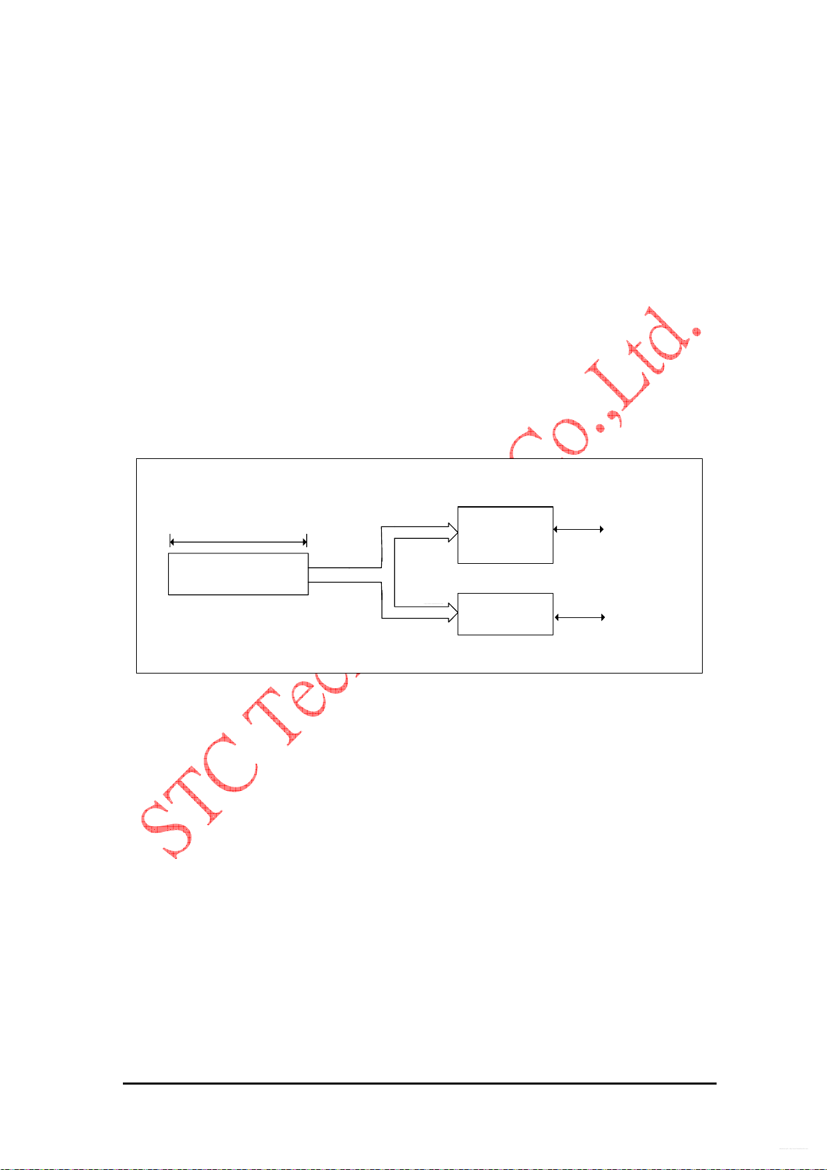
Programmable Counter Array (PCA)
http://www.DataSheet4U.net/
datasheet pdf - http://www.DataSheet4U.net/
The Programmable Counter Array is a special 16-bit Timer that has two 16-bit capture/compare modules
associated with it. Each of the modules can be programmed to operate in one of four modes:
z rising and/or falling edge capture (calculator of duty length for high/low pulse)
z software timer
z high-speed output
z pulse width modulator
Each module has a pin associated with it in port 1. Module-0 is connected to pin P1.3, module-1 to pin
P1.4.
The PCA timer is a common time base for all two modules and can be programmed to run at 1/12 the
oscillator frequency, 1/2 the oscillator frequency, the Timer-0 overflow or the input on pin ECI (P3.4). The
timer count source is determined from CPS1 and CPS0 bits in the SFR
16 Bit
PCA
Timer/Counter
Programmable Counter Array
Module-0
Capture/Compare
Register
Module-1
Capture/Compare
Register
CMOD.
P1.3/CEX0/
PCA0/PWM0
P1.4/CEX1/
PCA1/PWM1
In the CMOD SFR, there are two additional bits associated with the PCA. On of them is CIDL which
determines if to stop the PCA while the MCU is put under idle, the other bit is ECF which controls if to
pass the interrupt from PCA into the MCU.
The CCON SFR contains the run control bit for PCA and several flags for the PCA timer and each
module. To start the PCA counting, the CR bit (CCON.6) must be set by software; oppositely clearing bit
CR will shut off the PCA. There is a bit named CF in SFR CCON. The CF bit (CCON.7) will be set when
the PCA timer overflows, and an interrupt will be generated if the ECF (CMOD.0) is set. The CF bit can
only be cleared by software. There are two bits named CCF0 and CCF1 in SFR CCON. The CCF0 and
CCF1 serve as flags for module-0 and module-1 respectively. They are set by hardware when either a
match or a capture occurs. These flags also can only be cleared by software.
STC12C5Axx Technical Summary 45
Page 46

http://www.DataSheet4U.net/
datasheet pdf - http://www.DataSheet4U.net/
IDLE
Fosc/12
Fosc/2
Timer0 overflow
External input
ECI (P3.4)
--
PCA Timer/Counter
--CIDL
-
--CF
CH CL
CPS1 CP S0 ECF
- CCF1 CCF0CR
16-bit counter
CMOD
CCON
To PCA module
SFR: CMOD (PCA Mode Control Register)
Read/Write Address: 0xD9FH
PCA
interrupt
Default: 0XXX-X000
Bit 7 6 5 4 3 2 1 0
Name
CIDL CPS1 CPS0 ECF
CIDL := Behavior control of the PCA.
0 := (default)
Disable counting of the PCA counter while the MCU is put under idle state.
1 :=
Enable counting of the PCA counter while the MCU is put under idle state.
{ CPS1, CPS0 } := Used to select the clocking source for PCA counter
{ 0, 0 } := set the frequency of the PCA counter clock source as oscillator’s frequency over 12
{ 0, 1 } := set the frequency of the PCA counter clock source as oscillator’s frequency over 2
{ 1, 0 } := set the PCA counter clock source as Timer-0 overflow
{ 1, 1 } := set the PCA counter clock source as pin ECI(pin P3.4)
ECF := Control bit of deciding if to pass interrupt from PCA timer overflow to the MCU
0 := (default)
Inhibit the interrupt from PCA timer to the MCU
1 :=
Permit the interrupt from PCA timer to the MCU
46 STC12C5Axx Technical Summary
Page 47

STC TECHNOLOGY Co.,Ltd.
http://www.DataSheet4U.net/
datasheet pdf - http://www.DataSheet4U.net/
STC12C5A08/16/32/60
8-bit micro-controller
SFR: CCON (PCA Counter Control Rregister)
Read/Write Address: 0XD8FH
Default: 0XXX-X000
Bit 7 6 5 4 3 2 1 0
Name
CF CR CCF1 CCF0
CF := PCA Counter overflow Flag
This bit must be set by hardware itself. It can be cleared by software program.
CR := PCA Run control bit
0 := (default)
Disable counting of the PCA counter
1 :=
Start counting of the PCA counter
CCF1 := Module-1 interrupt Flag
This bit must be set by hardware itself when a match or capture from module-1 occurs.
It can be cleared by software program.
A match means the value of the PCA counter equals the value of the Capture/Compare
Register in the module-1.
A capture means a specific edge from CEX1 happens, so the Capture/Compare register
latches the value of the PCA counter, and the CCF1 is set.
CCF0 := Module-0 interrupt Flag
This bit must be set by hardware itself when a match or capture from module-0 occurs.
It can be cleared by software program.
Each module in the PCA has a special function register associated with it, CCAPM0 for
module0 and CCAPM1 for module-1. The register contains the bits that control the mode in
which each module will operate. The ECCFn bit controls if to pass the interrupt from CCFn
flag in the CCON SFR to the MCU when a match or compare occurs in the associated module.
PWMn enables the pulse width modulation mode. The TOGn bit when set causes the pin
CEXn output associated with the module to toggle when there is a match between the PCA
counter and the module’s Capture/Compare register. The match bit(MATn) when set will
cause the CCFn bit in the CCON register to be set when there is a match between the PCA
counter and the module’s Capture/Comp are register.
The next two bits CAPNn and CAPPn determine the edge type that a capture input will be
active on. The CAPNn bit enables the negative edge, and the CAPPn bit enables the positive
edge. If both bits are set, both edges will be enabled and a capture will occur for either
transition. The bit ECOMn when set enables the comparator function.
This document contains information on a new product under development by STC.STC reserves the right to change or discontinue this
product without notice. 2007/12 version A1
Page 48
http://www.DataSheet4U.net/
datasheet pdf - http://www.DataSheet4U.net/
SFR:
CL (PCA Base Counter Low Byte)
Read/Write Address: 0XE9H
Default: 0000-0000
Bit 7 6 5 4 3 2 1 0
Name
SFR: CH (PCA Base Counter High Byte)
Read/Write Address: 0XF9H
Default: 00000-0000
Bit 7 6 5 4 3 2 1 0
Name
SFR: CCAP0L (Low byte of PCA module-0 Compare/Capture register)
Read/Write Address: 0XEAH
Default: 0000-0000
Bit 7 6 5 4 3 2 1 0
Name
SFR: CCAP0H (High byte of PCA module-0 Compare/Capture register)
Read/Write Address: 0XFAH
Default: 0000-0000
Bit 7 6 5 4 3 2 1 0
Name
SFR: CCAP1L (Low byte of PCA module-1 Compare/Capture register)
Read/Write Address: 0XEBH
Default: 0000-0000
Bit 7 6 5 4 3 2 1 0
Name
SFR: CCAP1H (High byte of PCA module-1 Compare/Capture register)
Read/Write Address: 0XFBH
Default: 0000-0000
Bit 7 6 5 4 3 2 1 0
Name
48 STC12C5Axx Technical Summary
Page 49
STC TECHNOLOGY Co.,Ltd.
http://www.DataSheet4U.net/
datasheet pdf - http://www.DataSheet4U.net/
STC12C5A08/16/32/60
8-bit micro-controller
CCAPM0 (PCA Modul-0 Mode Register)
SFR:
Read/Write Address: 0XDAH
Default: X000-0000
Bit 7 6 5 4 3 2 1 0
Name
ECOM0 CAPP0 CAPNO MAT0 TOG0 PWM0 ECCF0
SFR: CCAPM1 (PCA Modul-1 Mode Register)
Read/Write Address: 0XDBH
Default: X000-0000
Bit 7 6 5 4 3 2 1 0
Name
ECOMn := used to determine if Enable Comparator
CAPPn: = configure the module-n’s register to latch the PCA counter on Positive edge of
CAPNn: = configure the module-n’s register to latch the PCA counter on Negative edge of
MATn: = used to determine if set the bit CCFn in SFR CCON while a match from module-n
TOGn: = Toggle the output pin
PWMn: = Enable plus width modulation mode n .
This document contains information on a new product under development by STC.STC reserves the right to change or discontinue this
product without notice. 2007/12 version A1
ECOM1 CAPP1 CAPN1 MAT1 TOG1 PWM1 ECCF1
0 := (default)
Disable the comparator function
1 :=
Enable the comparator function
EXIn or not
0 := (default)
configure the module-n’s register not to latch the PCA counter on CAPPn posedge.
1 :=
configure the module-n’s register to latch the PCA counter on CAPPn posedge.
EXIn or not
0 := (default)
configure the module-n’s register not to latch the PCA counter on pin CAPPn negedge.
1 :=
configure the module-n’s register to latch the PCA counter on pin CAPPn negedge.
occurs.
0 := (default)
Don’t set the bit CCFn while a match occurs between the PCA counter and module-n’s
register.
1 :=
Set the bit CCFn while a match occurs between the PCA counter and module-n’s
register.
0 := (default)
Don’t toggle the pin CEXn while a match occurs between the PCA counter and
module-n’s register.
1 :=
Toggle the pin CEXn while a match occurs between the PCA counter and
module-n’s register.
0 := (default)
Page 50

http://www.DataSheet4U.net/
datasheet pdf - http://www.DataSheet4U.net/
Inhibit the PWM functionality from module-n output to pin PWMn
1 :=
Enable the pin PWMn as the output of the PWM functionality from module-n
50 STC12C5Axx Technical Summary
Page 51
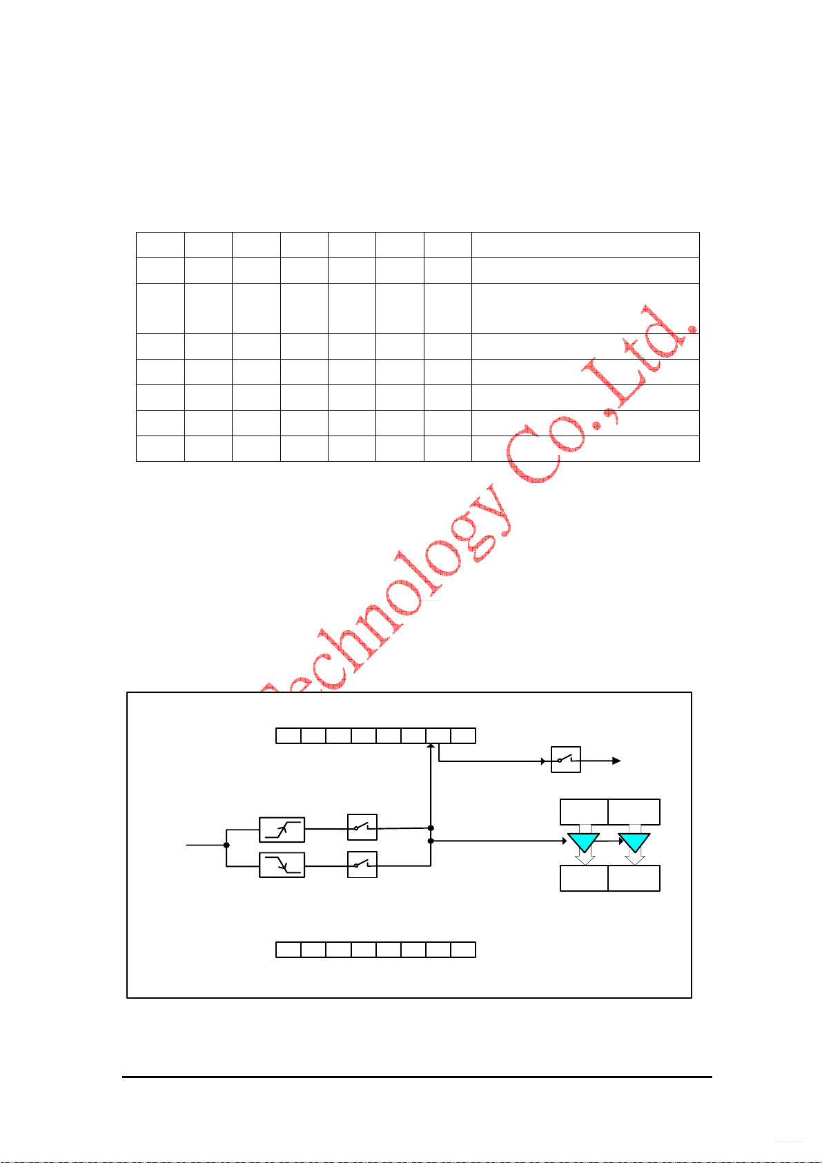
ECCFn: = Enable the CCFn flag in the CCON SFR to generate an interrupt.
http://www.DataSheet4U.net/
datasheet pdf - http://www.DataSheet4U.net/
0 := (default)
Inhibit the interrupt(CCFn) from module-n to the MCU
1 :=
Permit the interrupt(CCFn) from module-n to the MCU
Configure PCA Module
ECOMn CAPPn CAPNn MATn TOGn PWMn ECCFn Module function
0 0 0 0 0 0 0 No operation
X 1 0 0 0 0 X 16-bit capture by a positive-edge trigger on
CEXn
X 0 1 0 0 0 X 16-bit capture by a negative trigger on CEXn
X 1 1 0 0 0 X 16-bit capture by a transition on CEXn
1 0 0 1 0 0 X 16-bit Software Timer
1 0 0 1 1 0 X 16-bit High Speed Output
1 0 0 0 0 1 0 8-bit PWM
PCA Capture Mode
To use one of the PCA modules in the capture mode, one or both of bits CAPPn and CAPNn
in SFR CCAPMn should be set. The external CEXn input for the module is sampled for a
transition. When a valid transition occurs, the PCA hardware loads the value of the PCA
counter register(CH and CL) into the module’s capture registers(CCAPnH and CCAPnL). If
the bit CCFn for the module in the SFR CCON and the bit ECCFn in the SFR CCAPMn are
set then an interrupt will be generated.
CEXn
-
--CF
- CCF1 CCF0CR
CAPTURE
CCON
PCA
interrupt
CH CL
CCAPnH CCAPnL
-
0000
TOGn PWMn ECCFnECOMn CAPPn CAPNn MATn
MDnCON
PCA Capture Mode
STC12C5Axx Technical Summary 51
Page 52

http://www.DataSheet4U.net/
datasheet pdf - http://www.DataSheet4U.net/
16-bit Software Timer Mode
The PCA modules can be used as software timers by setting both the ECOMn and MATn bits
in the CCAPMn register. The PCA timer will be compared to the module’s capture registers
and when a match occurs an interrupt will be generated if the CCFn and ECCFn bits for the
module are both set.
High Speed Output Mode
In this mode the CEXn output (port latch) associated with the PCA module will toggle each
time a match occurs between the PCA counter and the module’s capture registers. To activate
this mode the TOGn, MATn, and ECOMn bits in the SFR CCAPMn must be set.
Pulse Width Modulator Mode
All of the PCA modules can be used as PWM outputs. The frequency of the output depends
on the PCA counter. All of the modules will have the same frequency of output because they
all share the PCA counter. The duty cycle of each module is independently variable using the
module’s capture register CCAPnL[7:0] and bits EPCnL in SFR PCAPWMn. When the value
of the SFR CL is less than the value in the module’s {EPCnL, CCAPnL [7:0]}, the output will
be low. When it is equal to or greater than, the output will be high. When CL overflows from
FF
to 00
H
, {EPCnL, CCAPnL [7:0 ]} is reloaded with the value in {EPCnH, CCAPnH [7:0]}.
H
That allows smoothly updating the PWM duty without glitches. The bits PWMn and ECOMn
bits in the CCAPMn must be set to enable the PWM mode.
SFR:
PCA_PWM0 (PCA PWM0 Auxiliary Register)
Read/Write Address: 0XF2H
Default: 0000-0000
Bit 7 6 5 4 3 2 1 0
Name
EPC0H EPC0L
SFR: PCA_PWM1 (PCA PWM1 Auxiliary Register)
Read/Write Address: 0XF3H
Default: 0000-0000
Bit 7 6 5 4 3 2 1 0
Name
CF CR EPC1H EPC1L
EPCnL: = concatenated with CCAPnL, used to control the duty of the PWM output
The bit EPCnL is going to be combined with CCAPnL to form a 9-bit data which will
be compared with PCA counter low byte CL, so to determine the duty of the module-n’s PWM
output.
If {CL[7:0]} < { EPCnL, CCAPnL[7:0]} , PWM output LOW
else PWM output HIGH
EPCnH: = Reloaded value of EPCnL while CL [7:0] counts from FF
to 00H
H
52 STC12C5Axx Technical Summary
Page 53

http://www.DataSheet4U.net/
datasheet pdf - http://www.DataSheet4U.net/
Write to CCAPnL
Write to CCAPnL
Write to CCAPnH
01
Enable
Write to CCAPnH
CCAPnH CCAPnL
16-bit
comparator
CH CL
-
PCA Software Timer Mode
-
-
MATCH
00
--CF
--CF
- CCF1 CCF0CR
CCON
PCA
interrupt
To CCFn
TOGn PWMn ECCFnECOMn C APPn CAPNn MATn
CCAPMn
00
- CCF1 CCF0CR
CCON
01
Enable
CCAPnH CCAPnL
16-bit
comparator
MATCH
CH CL
-
00
PCA High-Speed Ouput Mode
To CCFn
TOGn PWMn ECCFnECOMn C APPn CAPNn MATn
10
CCAPMn
Toggle
PCA
interrupt
CEXn
STC12C5Axx Technical Summary 53
Page 54
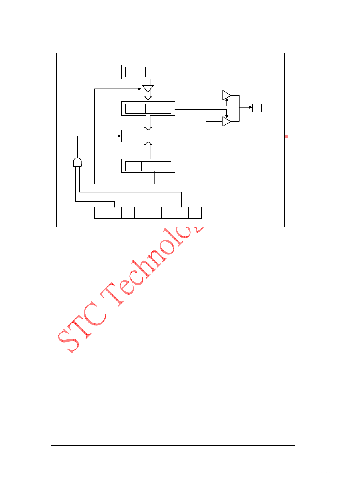
http://www.DataSheet4U.net/
datasheet pdf - http://www.DataSheet4U.net/
CCAPnHEPCnH
0
CCAPnLEPCnL
{0, CL [7:0]} < {EP CnL, CCAPnL[7:0]}
{0, CL [7:0]} >= {E PCnL, CCAPnL[7:0]}
1
CEXn
Enable
CL overflow
ECOMn CAPPn CAPNn M ATn TOGn PWMn ECCFn
9-BIT
COMPARATOR
0
0000 0
CL
PCA PWM mode
CCAPMn
54 STC12C5Axx Technical Summary
Page 55

STC TECHNOLOGY Co.,Ltd.
http://www.DataSheet4U.net/
datasheet pdf - http://www.DataSheet4U.net/
STC12C5A08/16/32/60
8-bit micro-controller
Serial Peripheral Interface(SPI)
The device provides another high-speed serial communication interface, the SPI interface. The SPI is a
full-duplex, high-speed, synchronous communication bus with two operation modes: Master mode and
Slave mode. Up to 3Mbit/s can be supported in either Master or Slave mode under the Fosc=12MHz.
Two status flags are provided to signal the transfer completion and write-collision occurrence.
P1.6
(MISO)
P1.5
(MOSI)
P1.7
(SPICLK)
P1.4
(SS)
Fosc
Clock Divider
4,
16,
64
128
Shift In Register
Shift Out Register
SPI Control
SPI block diagram
I/O control
SPR0SPR1CPHACPOLMSTRDORDSPENSSIG
------WCOLSPIF
SPICTL
SPISTAT
There are three pins implementing the SPI functionality, one of them is SCLK(P1.7), next is MISO(P1.6),
the other is MOSI(P1.5). An extra pin SS(P1.4) is designed to configure the SPI to run under Master or
Slave mode. Data flows from master to slave via MOSI(Master Out Slave In) pin and flows from slave to
master via MISO(Master In Slave Out) pin. The SCLK plays as an output pin when the device works
under Master mode, while as an input pin when the device works under Slave mode. If the SPI system is
disabled, i.e. SPEN(SPCTL.6)=0, these pins are configured as general-purposed I/O port(P1.4 ~ P1.7).
Two devices with SPI interface communicate with each other via one synchronous clock signal , one
input data signal, and one output data signal. There are two concerns the user could take care, one of
them is latching data on the negative edge or positive edge of the clock signal which named polarity, the
This document contains information on a new product under development by STC.STC reserves the right to change or discontinue this
product without notice. 2007/12 version A1
Page 56

http://www.DataSheet4U.net/
datasheet pdf - http://www.DataSheet4U.net/
other is keeping the clock signal low or high while the device idle which named phase. Permuting those
states from polarity and phase, there could be four modes formed, they are SPI-MODE-0, SPI-MODE-1,
SPI-MODE-2, SPI-MODE-3. Many device declares that they meet SPI mechanism, but few of them are
adaptive to all four modes. The STC12C5Axx is a device flexible to be configured to communicate to
another device with MODE-0, MODE-1, MODE-2 or MODE-3 SPI, and play part of Master and Slave.
There is a SFR named SPICTL designed to configure the SPI behavior of the device.
SFR:
SPCTL (SPI Control register)
Read/Write Address: 0X85H
Default: 0000-0000
Bit 7 6 5 4 3 2 1 0
Name
SSIG SPEN DORD MSTR CPOL CPHA SPR1 SPR0
SSIG := used to determine if Ignore the pin SS
0 := (default)
Reserve the function of pin SS
1 :=
Ignore the SS pin function
SPEN := Enable the SPI
0 := (default)
Disable the SPI function. All related pins play as general-purposed I/O ports.
1 :=
Enable the SPI function.
DORD := Data Order
0 := (default)
Transmit/Receive the MSB of the data byte first.
1 :=
Transmit/Receive the LSB of the data byte first.
MSTR := Set to Master mode
0 := (default)
Set the SPI to play as Slave part.
1 :=
Set the SPI to play as Master part.
CPOL := Clock Polarity
0 := (default)
Set the SPCLK as LOW while the communication is kept idle. That implies the leading
edge of the clock is the rising edge, and the trailing edge is the falling
edge.
56 STC12C5Axx Technical Summary
Page 57

1 :=
http://www.DataSheet4U.net/
datasheet pdf - http://www.DataSheet4U.net/
Set the SPCLK as HIGH while the communication is kept idle. That implies the leading
edge of the clock is the falling edge, and the trailing edge is the falling rising edge.
CPHA := Clock Phase
0 := (default)
Data is driven when pin SS is low and changes on the trailing edge of SPCLK,
and is sampled on the leading edge. (This setting is only valid while SSIG==0.)
1 :=
Data is driven on the leading edge of SPCLK, and is sampled on the trailing edge.
{SPR1, SPR0} := SPI clock Rate selector
{0,0} := (default)
Set the clock rate of the SPI as the frequency of the clock source over 4.
{0,1} :=
Set the clock rate of the SPI as the frequency of the clock source over 16.
{1,0} :=
Set the clock rate of the SPI as the frequency of the clock source over 64. {1,1} :=
Set the clock rate of the SPI as the frequency of the clock source over 128.
There are two extra SFRs make relation with SPI application.
SPDAT (SPI Data register)
SFR:
Read/Write Address: 0X86H
Default: 0000-0000
Bit 7 6 5 4 3 2 1 0
Name
The SFR SPDAT holds the data to be transmitted or the data received.
SFR: SPSTAT (SPI STATe register)
Read/Write Address: 0X84H
Default: 00XX-XXXX
Bit 7 6 5 4 3 2 1 0
Name
SPIF WCOL
SPIF := SPI transfer completion flag.
When a serial transfer finishes, the SPIF bit is set and an interrupt is generated if both the
ESPI(AUXR.3) bit and the EA(IE.7) bit are set. If SS is an input and is driven low when
SPI is in master mode with SSIG=0, SPIF will also be set to signal the “mode change”.
The SPIF is cleared in software by “writing 1 to this bit”.
WCOL := SPI Write Collision flag
STC12C5Axx Technical Summary 57
Page 58

http://www.DataSheet4U.net/
datasheet pdf - http://www.DataSheet4U.net/
The WCOL bit is set if the SPI data register SPIDAT is written during a data transfer. The
WCOL flag is cleared in software by “writing 1 to this bit”.
Configure the device to Master/Slave mode
SPEN SSIG SS MSTR Mode MISO MOSI SPICLK Remark
0 X X X SPI disable GPI/O GPI/O GPI/O SPI is disabled.
1 0 0 0 Active Salve output input input Selected as slave
1 0 1 0 InActive
Hi-Z input input Not selected.
Slave
1 0 0 1→0 slave output input input Convert from Master to
Slave
1 0 1 1 Master input output output SPCLK depends on
CPOL
1 1 X 0 Slave output input input Slave
1 1 X 1 Master input output output Master
58 STC12C5Axx Technical Summary
Page 59
Typical Connection
http://www.DataSheet4U.net/
datasheet pdf - http://www.DataSheet4U.net/
Master
Master/Slave
MISO MISO
MOSI MOSI
SPCLK
SPCLK
SSPort Pin
SPI single master sing l e slave configurartion
MISO MISO
MOSI MOSI
Slave/Master
SPCLK
SPCLK
Slave
SSSS
SPI dual device configuarion, where either can be a maste r or a slave
MISO MISO
MOSI MOSI
Slave #1
SPCLK
SPCLK
SSPort Pin 1
Master
MISO
MOSI
Slave #2
SPCLK
SSPort Pin 2
SPI single master multiple slaves configurartion
STC12C5Axx Technical Summary 59
Page 60

http://www.DataSheet4U.net/
datasheet pdf - http://www.DataSheet4U.net/
Communication
In SPI, transfers are always initiated by the master. If the SPI is enabled(SPEN=1) and selected as
master, any instruction that use SPI data register SPIDAT as the destination will starts the SPI clock
generator and a data transfer. The data will start to appear on MOSI about one half SPI bit-time to one
SPI bit-time after it. Before starting the transfer, the master may select a slave by driving the SS pin of
the corresponding device low. Data written to the SPDAT register of the master shifted out of MOSI pin
of the master to the MOSI pin of the slave. And at the same time the data in SPDAT register of the
selected slave is shifted out of MISO pin to the MISO pin of the master. During one byte transfer, data in
the master and in the slave is interchanged. After shifting one byte, the transfer completion flag(SPIF) is
set and an interrupt will be created if the SPI interrupt is enabled.
If SPEN=1, SSIG=0, SS pin=1 and MSTR=1, the SPI is enabled in master mode. Before the instruction
that use SPDAT as the destination register, the master is in idle state and can be selected as slave
device by any other master drives the idle master SS pin low. Once this happened, MSTR bit of the idle
master is cleared by hardware and changes its state a selected slave. User software should always
check the MSTR bit. If this bit is cleared by the mode change of SS pin and the user wants to continue to
use the SPI as a master later, the user must set the MSTR bit again, otherwise it will always stay in slave
mode.
The SPI is single buffered in transmit direction and double buffered in receive direction. New data for
transmission can not be written to the shift register until the previous transaction is complete. The WCOL
bit is set to signal data collision when the data register is written during transaction. In this case, the data
currently being transmitted will continue to be transmitted, but the new data which causing the collision
will be lost. For receiving data, received data is transferred into a internal parallel read data buffer so that
the shift register is free to accept a second byte. However, the received byte must be read from the data
register(SPDAT) before the next byte has been completely transferred. Otherwise the previous byte is
lost. WCOL can be cleared in software by “writing 1 to the bit”.
60 STC12C5Axx Technical Summary
Page 61

Typical Timing Diagram
http://www.DataSheet4U.net/
datasheet pdf - http://www.DataSheet4U.net/
Clock Cycle
SPCLK/CPOL=0
Driven from Master
SPCLK/CPOL=1
Driven from Master
MOSI (input)
Driven from Master
MISO (output)
SS pin (if SSIG bit = 0 )
Driven from Master
DORD=
DORD=
1 2345678
DORD=
MSB
65 4 3 21
LSB
12 3 4 56
65 4 3 21
12 3 4 56
0
1
0
DORD=
1
MOSI turns to input
MSB
LSB
MISO turns to output
SPI slave transfer format with CPHA=0
LSB
MSB
LSB
MSB
Clock
Cycle
SPCLK/CPOL=0
Driven from Master
SPCLK/CPOL=1
Driven from Master
MOSI (input)
Driven from Master
MISO (output)
SS pin (if SSIG bit = 0 )
Driven from Master
Clock Cycle
SPCLK/CPOL=0
SPCLK/CPOL=1
MOSI (Output)
MISO (Input)
Driven from the target
slave
Target slave SS pin
Control GPIO pin by software
DORD=
DORD=
MOSI turns to
DORD=
MSB
0
DORD=
LSB
1
MISO turns to
SPICLK is strongly output-driving.
SPEN=1 and MSTR=1, MOSI turns to ou tput data
MISO turns to input da ta
DORD=0
DORD=1
DORD=0
DORD=1
MSB
LSB
MSB
LSB
1 2345678
MSB
0
1
input
output
65 4 3 21
LSB
12 3 4 56
65 4 3 21
12 3 4 56
SPI slave transfer format with
CPHA=1
1 2345678
65 4 3 21
12 3 4 56
MOV SPDAT,#data in software
65 4 3 21
12 3 4 56
LSB
MSB
LSB
MSB
SPEN=0 or MSTR=0, MOSI switched not to output
data of SPI communication, also SPICLK is
released from SPI control
LSB
MSB
LSB
MSB
SS pin( if SSIG=0)
SPI master transfer format with CPHA=0
STC12C5Axx Technical Summary 61
Page 62

http://www.DataSheet4U.net/
datasheet pdf - http://www.DataSheet4U.net/
Clock Cycle
SPCLK/CPOL=0
SPCLK/CPOL=1
MOSI (Output)
MISO (Input)
Driven from the target slave
Target slave SS pin
Control GPIO pin by software
SS pin( if SSIG=0)
SPICLK is strongly output-
driving.
SPEN=1 and MSTR=1, MOSI turns to output
data
MISO turns to input
data
DORD=0
DORD=1
MSB
DORD=0
DORD=1
LSB
SPI master transfer format with CPHA=1
1 2345678
65 4 3 21
12 3 4 56
MOV SPDAT,#data in
software
MSB
65 4 3 21
LSB
12 3 4 56
LSB
MSB
LSB
MSB
SPEN=0 or MSTR=0, MOSI switched not to
outputdata of SPI communication, also SPICLK
isreleased from SPI
control
62 STC12C5Axx Technical Summary
Page 63
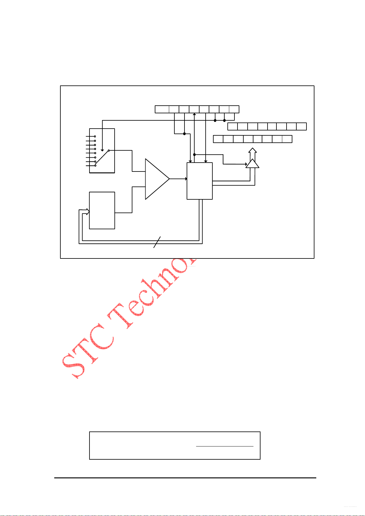
http://www.DataSheet4U.net/
datasheet pdf - http://www.DataSheet4U.net/
Analog to Digital Converter
ADC_POWE
R
P1.7(AI N7)
P1.6(AI N6)
P1.5(AI N5)
P1.4(AI N4)
P1.3(AI N3)
P1.2(AI N2)
P1.1(AI N1)
P1.0(AI N0)
+
-
Comparator
SPEED1
SPEED0ADC_
FLAG
Successive
Approximation
ADC_CONTR
ADC_
START
Regiter
CHS2 CHS1 CHS0
ADC_RESL
--
B9 B8 B7 B6 B5 B4 B3 B2
----
ADC_RES
B1 B0
10-b it DAC
10
The ADC on STC12C5Axx an 10-bit resolution, successive-approximation approach, medium-speed
A/D converter. V
REFP
/ V
is the positive/negative reference voltage input for internal voltage-scaling
REFM
DAC use, the typical sink current on it is 600uA ~ 1mA. For STC12C5A, these two references are
internally tied to VDD and GND, separately.
Conversion is invoked since ADC_START bit is set. Prior to ADC conversion, the desired I/O ports for
analog inputs should be configured as input-only or open-drain mode first. The conversion takes around
a fourth cycles to sample analog input data and other three fourths cycles in successive-approximation
steps. Total conversion time is controlled by two register bits – SPEED1 and SPEED0. Analog input
source comes from P1.
x, one of the eight-channels is multiplexed by analog multiplexer into the
comparator. When conversion is completed, the result will be saved onto {ADC_RES[7:0],
ADC_RESL[1:0]} register. After the result has been loaded onto {ADC_RES[7:0], ADC_RESL[1:0]}
register, ADC_FLAG will be set. ADC_FLAG associated with its enable register IE.5(EADC).
ADC_FLAG should be cleared in software. The ADC interrupt service routine vectors to 2B
. When the
H
chip enters idle mode or power-down mode, the power of ADC is turned off by hardware.
{ADC_RES,ADC_RESL[1:0] =
Vin – V
V
REFP
- V
REFM
REFM
STC12C5Axx Technical Summary 63
Page 64

STC TECHNOLOGY Co.,Ltd.
http://www.DataSheet4U.net/
datasheet pdf - http://www.DataSheet4U.net/
STC12C5A08/16/32/60
8-bit micro-controller
ADC_CONTR (ADC Control register)
SFR:
Read/Write Address: 0XECH
Default: 0XX0-0000
Bit 7 6 5 4 3 2 1 0
Name ADC_POWER SPEED1 SPEED0 ADC_FLAG ADC_START CHS2 CHAS1 CHS0
ADC_POWER :=
When clear shut down the power of ADC block. When set turn on the power of
ADC block.
{SPEED1, SPEED0} := Conversion speed selector
{0,0} := (default)
A conversion takes 840 clock cycles
{0,1} :=
A conversion takes 630 clock cycles
{1,0} :=
A conversion takes 420 clock cycles
{1,1} :=
A conversion takes 210 clock cycles
ADC_START := ADC Start control
Set to start an A/D conversion. It will be automatically cleared by the device after
the device has finished the conversion.
ADC_FLAG := ADC Interrupt flag
It will be set by the device after the device has finished a conversion, and should
be cleared by the user’s software.
{CHS2, CHS1, CHS0} := Input Channel Selector
{0,0,0} := (default)
Set P1.0 as the A/D channel input
{0,0,1} :=
Set P1.1 as the A/D channel input
{0,1,0} :=
Set P1.2 as the A/D channel input
{0,1,1} :=
Set P1.3 as the A/D channel input
{1,0,0} :=
Set P1.4 as the A/D channel input
{1,0,1} :=
Set P1.5 as the A/D channel input
{1,1,0} :=
Set P1.6 as the A/D channel input
{1,1,1} :=
Set P1.7 as the A/D channel input
This document contains information on a new product under development by STC.STC reserves the right to change or discontinue this
product without notice. 2007/12 version A1
Page 65

SFR: ADC_RES (ADC Value register):
http://www.DataSheet4U.net/
datasheet pdf - http://www.DataSheet4U.net/
Read/Write Address: 0XBDH
Default: 0000-0000
Bit 7 6 5 4 3 2 1 0
Name
The ADC_RES is the final result from the A/D conversion.
SFR: ADC_RESL (Low Byte of ADC Value register):
Read/Write Address: 0XBEH
Default: XXXX-XX00
Bit 7 6 5 4 3 2 1 0
Name
The ADC_RESL (Low Bytes of ADC Value register)
STC12C5Axx Technical Summary 65
Page 66

http://www.DataSheet4U.net/
datasheet pdf - http://www.DataSheet4U.net/
Power Management
IDLE Mode
An instruction setting PCON.0 causes the device go into the idle mode, the internal clock is
gated off to the CPU but not to the interrupt, timer, PCA, SPI, ADC, WDT and serial port
functions.
There are two ways to terminate the idle. Activation of any enabled interrupt will cause
PCON.0 to be cleared by hardware, terminating the idle mode. The interrupt will be serviced,
and following RETI instruction, the next instruction to be executed will be the one following the
instruction that puts the device into idle. Another way to wake-up from idle is to pull pin RST
high to generate internal hardware reset.
Save Power Consumption under IDLE Mode
A clock divider(CLKDIV) associated with idle mode is used to slow down the system clock
source in order to save power in advance. Everybody knows that slower the clock oscillates,
less power consumed. Software could program this clock divider register prior to enter the idle
mode. When the chip enters the idle mode, the clock is switched to the divider. When the
chip exits the idle mode, clocking will return to the original clock behavior.
SFR:
CLK_DIV (Power Control )
Read/Write Address: 0X97H
Default: XXXX-X000
Bit 7 6 5 4 3 2 1 0
Name CKS2 CKS1 CKS0
{CKS2, CKS1, CKS0}: Clock selector under idle mode
{0, 0,0} : = (default)
In idle mode, clock is not divided (default state)
{0, 0, 1} : =
In idle mode, clock is divided by 2
{0, 1, 0} : =
In idle mode, clock is divided by 4
{0, 1, 1} : =
In idle mode, clock is divided by 8
{1, 0,0} : =
In idle mode, clock is divided by 16
{1, 0, 1} : =
In idle mode, clock is divided by 32
{1, 1, 0} : =
In idle mode, clock is divided by 64
{1, 1, 1} : =
In idle mode, clock is divided by 128
66 STC12C5Axx Technical Summary
Page 67

POWER-DOWN Mode
http://www.DataSheet4U.net/
datasheet pdf - http://www.DataSheet4U.net/
An instruction setting PCON.1 causes the device go into the POWER-DOWN mode. In the
POWER-DOWN mode, the on-chip oscillator is stopped. The contents of on-chip RAM and
SFRs are maintained.
The power-down mode can be woken-up by either pin RST event or interrupt from INT0 or
INT1. When it is woken-up by RST, the program will execute from the address 0x0000. Be
carefully to keep RST pin active for at least 10ms in order for a stable clock. If it is woken-up
from pin INT0 or INT1, the CPU will rework through jumping to related interrupt service routine.
Before the CPU rework, the clock is blocked and counted until 32768 in order for de-bouncing
the unstable clock. To use INT0/INT1 wake-up, interrupt-related registers have to be enabled
and programmed accurately before entering power-down. Pay attention to add at least one
“NOP” instruction subsequent to the power-down instruction if I/O wake-up is used.
SFR: PCON (Power Control)
Read/Write Address: 0X897H
Default: XXXX-X000
Bit 7 6 5 4 3 2 1 0
Name SMOD SMOD0 LVDF POF GF1 GF0 PD IDL
SMOD: = Double baud rate of UART interface
0: =
Keep normal baud rate when the UART is used in mode 1,2 or 3.
1: =
Double baud rate when the UART is used in mode 1,2 or 3.
SMOD0:=
SM0/FE bit select for SFR SCON.7 ; Setting this bit will set SFR SCON.7 as Frame Error function.
Clearing it to set SCON.7 as one bit of UART mode selection bits.
(This bit is serial port related, see the further description about the serial port)
LVDF: = Low-Voltage Flag
After power-up, this bit will be initially set. The user should clear it by his program.
Continuously on operating, it will be set if the power supply drops under 3.7V/2.3V
(Operate in the 5V/3V).
POF: = Power-On flag
This bit will be set after the device was powered on.
It must be cleared by the user’s software.
PD: = Power-Down switch
Set this bit to drive the device enter
POWER-DOWN mode.
STC12C5Axx Technical Summary 67
Page 68

http://www.DataSheet4U.net/
datasheet pdf - http://www.DataSheet4U.net/
IDL: = Idle flag
Set this bit to drive the device enter
IDLE mode.
68 STC12C5Axx Technical Summary
Page 69
In System Programming and In Application Programming
http://www.DataSheet4U.net/
datasheet pdf - http://www.DataSheet4U.net/
In System Programming (ISP)
To develop a good program for ISP function, the user has to understand the architecture of the
embedded flash.
The embedded flash consists of 16 pages. Each page contains 512 bytes.
Dealing with flash, the user must erase it in page unit before writing (programming) data into
it.
Erasing flash means setting the content of that flash as FFh. Two erase modes are available
in this chip. One is mass mode and the other is page mode. The mass mode gets more
performance, but it erases the entire flash. The page mode is something performance less,
but it is flexible since it erases flash in page unit.
Unlike RAM’s real-time operation, to erase flash or to write (program) flash often takes long
time so to wait finish.
Furthermore, it is a quite complex timing procedure to erase/program flash. Fortunately, the
STC12C5Axx carried with convenient mechanism to help the user read/change the flash
content. Just filling the target address and data into several SFR, and triggering the built-in
ISP automation, the user can easily erase, read, and program the embedded flash.
There are several SFR designed to help the user implement the ISP functionality.
SFR:
IAP_DATA (ISP Flash Data register)
Bit-7 Bit-6 Bit-5 Bit-4 Bit-3 Bit-2 Bit-1 Bit-0
Data to be written into flash, or data got from flash
IFD is the data port register for ISP/IAP operation. The data in IFD will be written into the desired
address in operating ISP write and it is the data window of readout in operating ISP read.
SFR: IAP_ADDRH (ISP Flash Address High byte)
Bit-7 Bit-6 Bit-5 Bit-4 Bit-3 Bit-2 Bit-1 Bit-0
Must be cleared to 000 ISP/IAP address High byte
IFADRH is the high byte address for all ISP/IAP operation.
Against in advertise effect, if one bit of IFADRH [7:5] is set, the ISP write function must fail.
SFR: IAP_ADDRL (ISP Flash Address Low byte)
Bit-7 Bit-6 Bit-5 Bit-4 Bit-3 Bit-2 Bit-1 Bit-0
ISP/IAP address Low byte
IFADRL is the low byte address for all ISP/IAP operation.
SFR: IAP_CMD (ISP Flash-operating Mode Table)
Bit-7 Bit-6 Bit-5 Bit-4 Bit-3 Bit-2 Bit-1 Bit-0
- - - - -
-
Mode Selection
STC12C5Axx Technical Summary 69
Page 70

y
/
y
/
r
http://www.DataSheet4U.net/
datasheet pdf - http://www.DataSheet4U.net/
Mode Selection To Operate
0 0 Standby
0 1 AP-memory read
1 0 AP-memor
1 1 AP-memor
Data-flash program
Data-flash page erase
SFR: IAP_TRIG (ISP Sequential Command register to trigger ISP/IAP operation)
Bit-7 Bit-6 Bit-5 Bit-4 Bit-3 Bit-2 Bit-1 Bit-0
ISP-Command / Device ID
SFR: IAP_CONTR (IAP Control register)
Bit-7 Bit-6 Bit-5 Bit-4 Bit-3 Bit-2 Bit-1 Bit-0
IAPEN SWBS SWRST CFAIL - WAIT
IAPEN: = Determine if to Enable ISP/IAP functionality
0: =
Disable ISP program to change flash.
1: =
Enable ISP program to change flash.
SWBS: = Software Boot entrance Selector
0: =
Boot from main-memory.
1: =
Boot from ISP memory.
Note: This bit will be loaded with HWBS(OR0.3) after power-up moment.
SWRST: = Software Reset trigger
Setting this bit will cause the device reset.
CFAIL: = ISP/IAP Command Fail flag
0: =
The last ISP/IAP command has finished successfully.
1: =
The last ISP/IAP command fails. It could be caused since the access of flash memory
was inhibited.
WAIT: = Waiting time selection while the flash is busy.
CPU Wait time (Oscillato
IAP_CONTR[2:0] Page Erase Program Read Recommended
0 0 0 672384 1760 2 30M~24M
0 0 1 504288 1320 2 24M~20M
0 1 0 420240 1100 2 20M~12M
0 1 1 252144 660 2 12M~6M
1 0 0 126072 330 2 6M~3M
1 0 1 63036 165 2 3M~2M
1 1 0 42024 110 2 2M~1M
1 1 1 21012 55 2 < 1M
: Software reset actions could reset other SFR, but it never influences bits IAPEN
Notice
and SWBS. The ISPEN and SWBS only will be reset by power-up action, while
not software reset.
cycle)
System clock
70 STC12C5Axx Technical Summary
Page 71

STC TECHNOLOGY Co.,Ltd.
http://www.DataSheet4U.net/
datasheet pdf - http://www.DataSheet4U.net/
Procedures demonstrating ISP function
IAP_CMD ← xxxxx011
IAP_CONTR
IAP_ADDRH
IAP_ADDRL
IAP_TRIG ← 5Ah /* trig IAP activity */
IAP_TRIG ← A5h
(CPU progressing will be hold here )
(CPU continues)
← 100xx010
← (page address high byte) /* specify the address of the page to be erased */
← (page address low byte)
/* choice page-erasing command */
B
/* set ISPEN=1 to enable flash change.
B
set WAIT=010, 10942 MC; assumed 10M X’s*/
Erase a specific flash page
STC12C5A08/16/32/60
8-bit micro-controller
IAP_CMD ← xxxxx010
IAP_CONTR
← 100xx010
X’s*/
IAP_ADDRH
IAP_ADDRL
IAP_DATA ← (byte date to be written into flash) /* prepare data source */
IAP_TRIG
IAP_TRIG
(CPU progressing will be hold here)
(CPU continues)
← (Address high byte) /* specify the address to be programmed */
← (Address low byte)
← 5Ah /* trig IAP activity */
← A5h
/* choice byte-programming command */
B
/* set ISPEN=1 to enable flash change.
B
set WAIT=010, 60 MC; assumed 10M
IAP_CMD ← xxxxx001
IAP_CONTR
IAP_ADDRH
IAP_ADDRL
IAP_TRIG ← 5Ah /* trig ISP activity */
IAP_TRIG ← A5h
(CPU progressing will be hold here)
(CPU continues and currently IAP_DATA contain the desired data byte )
← 100xx010
set WAIT=010, 11 MC; assumed 10M X’s*/
← (Address high byte) /* specify the address to be read */
← (Address low byte)
Program a byte into flash
/* choice byte-read command */
B
/* set IAPEN=1 to enable flash change.
B
Read a byte from flash
This document contains information on a new product under development by STC.STC reserves the right to change or discontinue this
product without notice. 2007/12 version A1
Page 72
STC TECHNOLOGY Co.,Ltd.
http://www.DataSheet4U.net/
datasheet pdf - http://www.DataSheet4U.net/
STC12C5A08/16/32/60
8-bit micro-controller
In-Application Program (IAP)
The In-Application Program feature is designed for user to Read/Write nonvolatile data flash.
It may bring great help to store parameters those should be independent of power-up and
power-done action. In other words, the user can store data in data flash memory, and after he
shutting down the MCU and rebooting the MCU, he can get the original value, which he had
stored in.
The user can program the data flash according to the same way as ISP program, so he should
get deeper understanding related to SFR IAP_DATA, IAP_ADDRL, IAP_ADDRH, IAPCMD,
IAP_TRIG, and IAP_CONTR.
The data flash can be programmed by the AP program as well as the ISP program.
The ISP program may program the AP memory and data flash, while the AP program may
program the data flash but not the ISP memory. If the AP program desires to change the ISP
memory associated with specific address space, the hardware will ignore it.
Instructions Set
DATA TRASFER
MNEMONIC DESCRIPTION BYT CYC
MOV A, Rn Move register to Acc 1 1
MOV A, direct Move direct byte o Acc 2 2
MOV A, @Ri Move indirect RAM to Acc 1 2
MOV A, #data Move immediate data to Acc 2 2
MOV Rn, A Move Acc to register 1 2
MOV Rn, direct Move direct byte to register 2 4
MOV Rn, #data Move immediate data to register 2 2
MOV direct, A Move Acc to direct byte 2 3
MOV direct, Rn Move register to direct byte 2 3
MOV direct, direct Move direct byte to direct byte 3 4
MOV direct, @Ri Move indirect RAM to direct byte 2 4
MOV direct, #data Move immediate data to direct byte 3 3
MOV @Ri, A Move Acc to indirect RAM 1 3
MOV @Ri, direct Move direct byte to indirect RAM 2 3
MOV @Ri, #data Move immediate data to indirect RAM 2 3
MOV DPTR,#data16 Load DPTR with a 16-bit constant 3 3
MOVC A,@A+DPTR Move code byte relative to DPTR to Acc 1 4
MOVC A,@A+PC Move code byte relative to PC to Acc 1 4
PUSH direct PUSH DIRECT BYTE ONTO STACK 2 4
POP direct POP DIRECT BYTE FROM STACK 2 3
XCH A, Rn EXCHANGE REGISTER WITH ACC 1 3
XCH A, direct EXCHANGE DIRECT BYTE WITH ACC 2 4
XCH A, @Ri EXCHANGE INDIRECT RAM WITH ACC 1 4
XCHD A, @Ri EXCHANGE LOW-ORDER DIGIT INDIRECT RAM WITH ACC 1 4
This document contains information on a new product under development by STC.STC reserves the right to change or discontinue this
product without notice. 2007/12 version A1
Page 73

http://www.DataSheet4U.net/
datasheet pdf - http://www.DataSheet4U.net/
ARITHEMATIC OPERATIONS
MNEMONIC DESCRIPTION BYT CYC
ADD A, Rn ADD REGISTER TO ACC 1 2
ADD A, direct ADD DIRECT BYTE TO ACC 2 3
ADD A, @Ri ADD INDIRECT RAM TO ACC 1 3
ADD A, #data ADD IMMEDIATE DATA TO ACC 2 2
ADDC A, Rn ADD REGISTER TO ACC WITH CARRY 1 2
ADDC A, direct ADD DIRECT BYTE TO ACC WITH CARRY 2 3
ADDC A, @Ri ADD INDIRECT RAM TO ACC WITH CARRY 1 3
ADDC A, #data ADD IMMEDIATE DATA TO ACC WITH CARRY 2 2
SUBB A, Rn SUBTRACT REGISTER FROM ACC WITH BORROW 1 2
SUBB A, direct SUBTRACT DIRECT BYTE FROM ACC WITH BORROW 2 3
SUBB A, @Ri SUBTRACT INDIRECT RAM FROM ACC WITH BORROW 1 3
SUBB A, #data SUBTRACT IMMEDIATE DATA FROM ACC WITH BORROW 2 2
INC A INCREMENT ACC 1 2
INC Rn INCREMENT REGISTER 1 3
INC direct INCREMENT DIRECT BYTE 2 4
INC @Ri INCREMENT INDIRECT RAM 1 4
DEC A DECREMENT ACC 1 2
DEC Rn DECREMENT REGISTER 1 3
DEC direct DECREMENT DIRECT BYTE 2 4
DEC @Ri DECREMENT INDIRECT RAM 1 4
INC DPTR INCREMENT DPTR 1 1
MUL AB MULTIPLY A AND B 1 4
DIV AB DIVIDE A BY B 1 5
DA A DECIMAL ADJUST ACC 1 4
LOGIC OPERATION
MNEMONIC DESCRIPTION BYT CYC
ANL A, Rn AND REGISTER TO ACC 1 2
ANL A, direct AND DIRECT BYTE TO ACC 2 3
ANL A, @Ri AND INDIRECT RAM TO ACC 1 3
ANL A, #data AND IMMEDIATE DATA TO ACC 2 2
ANL direct, A AND ACC TO DIRECT BYTE 2 4
ANL direct, #data AND IMMEDIATE DATA TO DIRECT BYTE 3 4
ORL A, Rn OR REGISTER TO ACC 1 2
ORL A, direct OR DIRECT BYTE TO ACC 2 3
ORL A, @Ri OR INDIRECT RAM TO ACC 1 3
ORL A, #data OR IMMEDIATE DATA TO ACC 2 2
ORL direct, A OR ACC TO DIRECT BYTE 2 4
ORL direct, #data OR IMMEDIATE DATA TO DIRECT BYTE 3 4
XRL A, Rn EXCLUSIVE-OR REGISTER TO ACC 1 2
XRL A, direct EXCLUSIVE-OR DIRECT BYTE TO ACC 2 3
XRL A, @Ri EXCLUSIVE-OR INDIRECT RAM TO ACC 1 3
XRL A, #data EXCLUSIVE-OR IMMEDIATE DATA TO ACC 2 2
XRL direct, A EXCLUSIVE-OR ACC TO DIRECT BYTE 2 4
XRL direct, #data EXCLUSIVE-OR IMMEDIATE DATA TO DIRECT BYTE 3 4
CLR A CLEAR ACC 1 1
CPL A COMPLEMENT ACC 1 2
RL A ROTATE ACC LEFT 1 1
RLC A ROTATE ACC LEFT THROUGH THE CARRY 1 1
RR A ROTATE ACC RIGHT 1 1
RRC A ROTATE ACC RIGHT THROUGH THE CARRY 1 1
SWAP A SWAP NIBBLES WITHIN THE ACC 1 1
BOOLEAN VARIABLE MANIPULATION
MNEMONIC DESCRIPTION BYT CYC
CLR C CLEAR CARRY 1 1
CLR bit CLEAR DIRECT BIT 2 4
SETB C SET CARRY 1 1
SETB bit SET DIRECT BIT 2 4
CPL C COMPLEMENT CARRY 1 1
CPL bit COMPLEMENT DIRECT BIT 2 4
ANL C, bit AND DIRECT BIT TO CARRY 2 3
STC12C5Axx Technical Summary 73
Page 74

http://www.DataSheet4U.net/
datasheet pdf - http://www.DataSheet4U.net/
ANL C, /bit AND COMPLEMENT OF DIRECT BIT TO CARRY 2 3
ORL C, bit OR DIRECT BIT TO CARRY 2 3
ORL C, /bit OR COMPLEMENT OF DIRECT BIT TO CARRY 2 3
MOV C, bit MOVE DIRECT BIT TO CARRY 2 3
MOV bit, C MOVE CARRY TO DIRECT BIT 2 4
BOOLEAN VARIABLE BRANCH
MNEMONIC DESCRIPTION BYT CYC
JC rel JUMP IF CARRY IS SET 2 3
JNC rel JUMP IF CARRY NOT SET 2 3
JB bit, rel JUMP IF DIRECT BIT IS SET 3 4
JNB bit, rel JUMP IF DIRECT BIT NOT SET 3 4
JBC bit, rel JUMP IF DIRECT BIT IS SET AND THEN CLEAR BIT 3 5
PROAGRAM BRACHING
MNEMONIC DESCRIPTION BYT CYC
ACALL addr11 ABSOLUTE SUBROUTINE CALL 2 6
LCALL addr16 LONG SUBROUTINE CALL 3 6
RET RETURN FROM SUBROUTINE 1 4
RETI RETURN FROM INTERRUPT SUBROUTINE 1 4
AJMP addr11 ABSOLUTE JUMP 2 3
LJMP addr16 LONG JUMP 3 4
SJMP rel SHORT JUMP 2 3
JMP @A+DPTR JUMP INDIRECT RELATIVE TO DPTR 1 3
JZ rel JUMP IF ACC IS ZERO 2 3
JNZ rel JUMP IF ACC NOT ZERO 2 3
CJNE A, direct, rel COMPARE DIRECT BYTE TO ACC AND JUMP IF NOT EQUAL 3 5
CJNE A, #data, rel COMPARE IMMEDIATE DATA TO ACC AND JUMP IF NOT EQUAL 3 4
CJNE Rn, #data, rel
CJNE @Ri, #data, rel COMPARE IMMEDIATE DATA TO INDIRECT RAM AND JUMP IF NOT 3 5
EQUAL
DJNZ Rn, rel DECREMENT REGISTER AND JUMP IF NOT EQUAL 2 4
DJNZ direct, rel DECREMENT DIRECT BYTE AND JUMP IF NOT EQUAL 3 5
NOP NO OPERATION 1 1
MNEMONIC DESCRIPTION BYT CYC
MOVX A, @Ri Move external RAM(8-bit address) to Acc 1 3
MOVX A, @DPTR MOVE EXTERNAL RAM(16-BIT ADDRESS) TO ACC 1 2
MOVX @Ri, A MOVE ACC TO EXTERNAL RAM(8-BIT ADDRESS) 1 3
MOVX @DPTR, A MOVE ACC TO EXTERNAL RAM(16-BIT ADDRESS) 1 2
COMPARE IMMEDIATE DATA TO REGISTER AND JUMP IF NOT
EQUAL
****** INHIBITED INSTRUCTION ******
3 4
74 STC12C5Axx Technical Summary
Page 75
Absolute Maximum Rating (STC12C5Axx)
http://www.DataSheet4U.net/
datasheet pdf - http://www.DataSheet4U.net/
Parameter Rating
Operating Voltage 4.5V ~ 5.5V
Operating temperature under bias -40oC ~ 85oC*1
Storage temperature -40oC ~ 125oC
Voltage on any pin -0.5 ~ 5.5V
Operating Frequency DC ~ 25MHz
*1
Tested by sampling
DC Characteristics
VSS = 0V, TA = 25 ℃, V
CC
(STC12C5Axx)
= 5.0V
unless otherwise specified
Symbol Parameter Test
Condition
V
IH1
V
IH2
Input High voltage for P1 and P3
Input High voltage for RESET pin
VIL Input Low voltage
IOL Output Low current V
I
Output High current(push-pull) V
OH1
I
Output High current(Quasi-bidirectional) V
OH2
I
Logic 0 input current(Quasi-bidirectional) V
IL1
I
Logic 0 input current(Input-Only) V
IL2
ILK Input Leakage current(Open-Drain output) V
I
Logic 1 to 0 transition current V
H2L
IOP Operating current F
I
Idle mode current F
IDLE
IPD Power down current V
Vcc=5.0V
Vcc=5.0V
Vcc=5.0V
=0.45V 12 20 mA
PIN
=2.4V 12 20 mA
PIN
=2.4V 220 uA
PIN
=0.45V 17 50 uA
PIN
=0.45V 0 10 uA
PIN
= VCC 0 10 uA
PIN
=1.8V 230 500 uA
PIN
= 12MHz 12 30 mA
OSC
= 12MHz 6 15 mA
OSC
=5.0V 0.1 50 uA
CC
Limits Unit
min typ max
2.0 V
3.5 V
0.8 V
R
Internal reset pull-down resistance V
RST
=5.0V 100 Kohm
CC
STC12C5Axx Technical Summary 75
Page 76
http://www.DataSheet4U.net/
datasheet pdf - http://www.DataSheet4U.net/
Absolute Maximum Rating (STC12LE5Axx)
Parameter Rating
Operating Voltage 2.4V ~ 3.6V
Operating temperature under bias -40oC ~ 85oC*1
Storage temperature -40oC ~ 125oC
Voltage on any pin -0.5 ~ 3.6V
Operating Frequency DC ~ 25MHz
*1
Tested by sampling
DC Characteristics
VSS = 0V, TA = 25 ℃, V
CC
(STC12LE5Axx)
= 3.3V
unless otherwise specified
Symbol Parameter Test
Condition
V
IH1
V
IH2
Input High voltage for P1 and P3
Input High voltage for RESET pin
VIL Input Low voltage
IOL Output Low current V
I
Output High current(push-pull) V
OH1
I
Output High current(Quasi-bidirectional) V
OH2
I
Logic 0 input current(Quasi-bidirectional) V
IL1
I
Logic 0 input current(Input-Only) V
IL2
ILK Input Leakage current(Open-Drain output) V
I
Logic 1 to 0 transition current(P1,3) V
H2L
IOP Operating current F
I
Idle mode current F
IDLE
IPD Power down current V
Vcc=3.3V
Vcc=3.3V
Vcc=3.3V
=0.45V 8 14 mA
PIN
=2.4V 4 8 mA
PIN
=2.4V 64 uA
PIN
=0.45V 7 50 uA
PIN
=0.45V 0 10 uA
PIN
= VCC 0 10 uA
PIN
=1.4V 100 600 uA
PIN
= 12MHz 9 15 mA
OSC
= 12MHz 3.5 6 mA
OSC
=3.3V 0.1 50 uA
CC
Limits Unit
min typ max
2.0 V
2.8 V
0.8 V
R
Internal reset pull-down resistance V
RST
=3.3V 100 Kohm
CC
76 STC12C5Axx Technical Summary
Page 77

Package Dimension
http://www.DataSheet4U.net/
datasheet pdf - http://www.DataSheet4U.net/
STC12C5Axx Technical Summary 77
Page 78
http://www.DataSheet4U.net/
datasheet pdf - http://www.DataSheet4U.net/
Version History
Version Date Page Description
A1 2008/09
Initial issue
-
-
-
78 STC12C5Axx Technical Summary
 Loading...